control signal based full adder/subtractor...control signal based full adder/subtractor sugandha g a...
TRANSCRIPT
Control Signal Based Full Adder/Subtractor Sugandha Gaur M.Tech Scholar
VLSI design , JECRC University, Jaipur
Abhilasha Assistant Professor
JECRC University, Jaipur
[email protected] Abstract :- Reversible Logics are very important and
useful for the future computational technologies.
Reversible Logic is an important Research Area which is
using for CMOS design with Low Power. In this Paper, we
are applying MIG and COG Reversible Logic Gate based
Fault Tolerant Ful Adder/ Subtractor. Results are showing
regarding Delay. The delay is reducing for the MIG and
COG Gate based Full Adder/Subtractor.
Keywords- COG, delay Reversible gate ,Feynman double gate,
Fredkin gate, full adder, MIG.
I. INTRODUCTION
Reversible Logic Gates are using mostly in VLSI Domain for
Design CMOS Circuit just due to Low Power Capability and
low delay property. In the Present time, Quantum Computers
are using Reversible Logic Gates. Reversible Logic Gates
have lots of applications like low power CMOS. Optical
important processing, Quantum Computational, DNA-based
computing and Nano Technology. In 1960 R.Landaurer's
presented that design system by using Irreversible Hardware
design is showing energy consumption and information design
is showing high energy consumption and information loss.
A Process, in which impulses reduced to output is called
reversible logic; Irreversibility logic gate is the primary factor
for dissipation more Power Consumption. The most important
computational in energy. Reversible Logic Gate are related to
the Power when Landauer[1], prove that loss of information
occurs from the irreversibility of function to power
consumption in 1961. They inform that Power consumption in
the circuit is getting due to one bit Loss information and equal
to KITn2 . Here k is a Boltzmann Constant while T is a
Temperature. In the 1973, they give the rule that Reversible
Logic Gate can reduce power consumption. In the theorem,
they prove that power consumption will not perform from the
circuit if input extract from the output and reversible logic
gate might be used.
II. REVERSIBLE GATES
A. Basic Reversible Gates
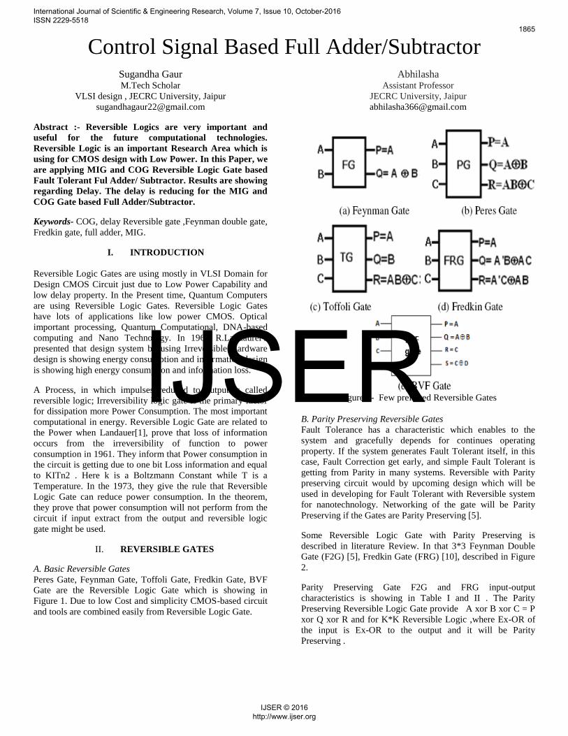
Peres Gate, Feynman Gate, Toffoli Gate, Fredkin Gate, BVF
Gate are the Reversible Logic Gate which is showing in
Figure 1. Due to low Cost and simplicity CMOS-based circuit
and tools are combined easily from Reversible Logic Gate.
Figure1:- Few preferred Reversible Gates
B. Parity Preserving Reversible Gates
Fault Tolerance has a characteristic which enables to the
system and gracefully depends for continues operating
property. If the system generates Fault Tolerant itself, in this
case, Fault Correction get early, and simple Fault Tolerant is
getting from Parity in many systems. Reversible with Parity
preserving circuit would by upcoming design which will be
used in developing for Fault Tolerant with Reversible system
for nanotechnology. Networking of the gate will be Parity
Preserving if the Gates are Parity Preserving [5].
Some Reversible Logic Gate with Parity Preserving is
described in literature Review. In that 3*3 Feynman Double
Gate (F2G) [5], Fredkin Gate (FRG) [10], described in Figure
2.
Parity Preserving Gate F2G and FRG input-output
characteristics is showing in Table I and II . The Parity
Preserving Reversible Logic Gate provide A xor B xor C = P
xor Q xor R and for K*K Reversible Logic ,where Ex-OR of
the input is Ex-OR to the output and it will be Parity
Preserving .
International Journal of Scientific & Engineering Research, Volume 7, Issue 10, October-2016 ISSN 2229-5518
1865
IJSER © 2016 http://www.ijser.org
IJSER

(a) (b)
Figure 2:- (a)Feynman Double Gate (F2G), (b) Fredkin
Gate(FRG)
TABLE I. Table of Parity Preserving Feynman Double Gate
(F2G)
A B C P Q R
0 0 0 0 0 0
0 0 1 0 0 1
0 1 0 0 1 0
0 1 1 0 1 1
1 0 0 1 1 1
1 0 1 1 1 0
1 1 0 1 0 1
1 1 1 1 0 0
TABLE II. Table of Parity Preserving Fredkin Gate (FRG)
A B C P Q R
0 0 0 0 0 0
0 0 1 0 0 1
0 1 0 0 1 0
0 1 1 0 1 1
1 0 0 1 0 0
1 0 1 1 1 0
1 1 0 1 0 1
1 1 1 1 1 1
Implementation of Reversible Logic has been described in the
Literature of the Paper. Reversible Adder circuit is shown by
at least two Garbage Output with one constant input. For Fault
Tolerant Reversible Logic Gate requirement is not same. Due
to Parity input match with output Parity for a Fault Tolerant
Adder circuit. In the section, we describe Half Adder/
Subtractor module while another circuit is designed for
minimum Garbage output number and Constant input.
C. Design of Half Adder/Subtractor Circuit (FTHA_S)
The basic for the Parity Preserving Reversible Gate Feynman
Gate and Fredkin Gate have been explained for the Half adder
is
Sum = A Xor B …..(1)
Carry = A and B …..(2)
Half Subtractor Boolean Expression is
Difference = A Xor B ….. (3)
𝐵𝑜𝑟𝑟𝑜𝑤 = ((𝑁𝑜𝑡 𝐴)𝑎𝑛𝑑 𝐵) … . (4)
From the equation (1) and (3), we can see that both are the
same. The difference is in between Carry and Borrow. In this
Section, we design both Adder / Subtractor. In this Adder /
Subtractor, 0 is using for addition and Logic 1 is using for
subtraction. From the Figure 3, we can check that there are
three input A, B, and Cntrl signal. The control signal is using
for control the operation of addition and subtraction.
In Figure 3 , S/D is Sum/Difference while C/B is defined as
carry and Borrow. Remaining all the other outputs are
Garbage Value. For Design the Half Adder / Subtractor two
F2G reversible gate and 2 FRG gates are using. Figure 4 is
showing the Fault Tolerance Half Adder / Subtractor Block
Diagram. In this Block Diagram A, B, Cntrl are the input and
seven output where S/D and C/B are the output.
S/D = A Xor B ......(5) C/B = ((Not Cntrl ) and A and B ) or ( Cntrl and (Not A ) and B )
.....(6)
Figure 3. Circuit of reversible fault tolerant Half
Adder/Subtractor
Figure 4. Half Adder/Subtarctor circuit with four constant
inputs & five garbage outputs
D. Design of Full Adder/Subtarctor Circuit (FTFA_S)
Conventional Approach is using for design Full Adder/
Subtractor. In this Conventional Approach, two Half Adder
circuit are using. The Block Diagram of the Fault Tolerant
Full Adder/ Subtractor is showing in Fig 5. The expression is
shown as
International Journal of Scientific & Engineering Research, Volume 7, Issue 10, October-2016 ISSN 2229-5518
1866
IJSER © 2016 http://www.ijser.org
IJSER
Sum = A Xor B Xor C .....(7)
Carry = ((A Xor B ) and Cin) Xor ( A and B) .....(8)
The expression for full subtractor is:
Difference = A Xor B Xor C .....(9)
Borrow = ((Not A) And B ) or ( B and C) or (C and (Not A))
....(10)
As we can see in Figure 5 , A, B , C, Cntrl signals are the
input. In the Full Adder / Subtractor, three inputs A, B, C are
using while Cntrl signal is using for control the operation of
the Adder/Subtraction. When the Control signal is 0 then
addition will perform, and when the Control Signal is 1 then
Subtraction will perform S/D, and C/B are the Sum and
Difference, Carry and Borrow. In this Design, we are using
two Half Adder / Subtraction while one F2G Gate.
Figure 5. Circuit of reversible fault tolerant Full Adder/Subtractor
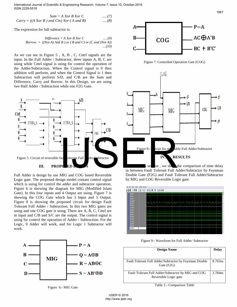
III. PROPOSED DESIGN
Full Adder is design by use MIG and COG based Reversible
Logic gate. The proposed design model contain control signal
which is using for control the adder and subtractor operation.
Figure 6 is showing the diagram for MIG (Modified Islam
Gate). In this four inputs and 4 Output are using. Figure 7 is
showing the COG Gate which has 3 Input and 3 Output.
Figure 8 is showing the proposed circuit for design Fault
Tolerant Full Adder / Subtraction. In this two MIG gates are
using and one COG gate is using. There are A, B, C, Cntrl are
in input and C/B and S/C are the output. The control signal is
using for control the operation of Adder / Subtraction. For the
Logic, 0 Adder will work, and for Logic 1 Subtractor will
work.
Figure 6:- MIG Gate
Figure 7: Controlled Operation Gate (COG)
Figure 8:- Circuit for reversible Full Adder/Subtractor
IV. RESULTS
In the results session , we show the comparison of time delay
in between Fault Tolerant Full Adder/Subtractor by Feynman
Double Gate (F2G) and Fault Tolerant Full Adder/Subtractor
by MIG and COG Reversible Logic gate.
Figure 9:- Waveform for Full Adder/ Subtractor
Design Name Delay
Fault Tolerant Full Adder/Subtractor by Feynman Double
Gate (F2G)
8.765ns
Fault Tolerant Full Adder/Subtractor by MIG and COG
Reversible Logic gate
3.784ns
Table 1:- Comparison Table
International Journal of Scientific & Engineering Research, Volume 7, Issue 10, October-2016 ISSN 2229-5518
1867
IJSER © 2016 http://www.ijser.org
IJSER
Table 1 is showing the comparison for the Fault Tolerant full
Adder / Subtractor and MIG / COG reversible logic Gate
based Full Adder/ Subtractor . As we can check from the
Table 1 the delay is low for the proposed Design .
V. CONCLUSION
In this paper, we introduce the Fault Tolerant Full
Adder/Subtractor by Reversible Logic gate with low delay for
improve the performance of the fast adder and Subtractor . We
introduce the Fault Tolerant Full Adder/Subtractor by MIG
and COG Reversible Logic gate with low delay for improve
the performance of the fast adder and Subtractor
REFERENCES
[1]. Parminder Kaur & Balwinder singh Dhaliwal," Design of
Fault Tolearnt Full Adder/Subtarctor Using Reversible Gates"
International Conference on Computer Communication and
Informatics (ICCCI) -2012.
[2]. Prashanth. N. G, Havyas. V. B, Prashantha. N. C,
Naveena Pai G4, Dinesha Shetty G," Design of Efficient
Reversible Fault Tolerant Carry Skip Adder/Subtractor"
International Journal of Emerging Technology and Advanced
Engineering, Volume 3, Issue 11, November 2013.
[3]. Ankur Sarker, Avishek Bose, Shalini Gupta," Design of a
Compact Fault Tolerant Adder/Subtractor Circuits Using
Parity Preserving Reversible Gates ", 17th Int'l Conf. on
Computer and Information Technology, 22-23 December
2014.
[4]. Dondapati Naresh, V.B.Gopala Krishna,"Design and
Implementation of Fault Tolerant Carry Skip Adder or
Subtractor using Reversible Logic Gates", ISSN 2322-0929
Vol.02, Issue.07, October-2014.
[5]. S.Mounika, Dr.M.Gurunandabaabu," A Novel Design for
carry skip adder using purity preserving reversible logic gates
", International Journal & Magazine of Engineering,
Technology, Management and Research, Volume No: (2015).
[6]. Subramanian Saravanan1, Ila Vennila, Sudha Mohanram,"
Design and Implementation of an Efficient Reversible
Comparator Using TR Gate ", Circuits and Systems, 2016.
International Journal of Scientific & Engineering Research, Volume 7, Issue 10, October-2016 ISSN 2229-5518
1868
IJSER © 2016 http://www.ijser.org
IJSER