concepts and components for pulsed angle modulated...
TRANSCRIPT

Chapter 0
Concepts and Components forPulsed Angle Modulated Ultra WidebandCommunication and Radar Systems
Alexander Esswein, Robert Weigel, Christian Carlowitz and Martin Vossiek
Additional information is available at the end of the chapter
http://dx.doi.org/10.5772/55082
1. Introduction
Ultra Wideband (UWB) systems have been utilized and commercialized since the beginning ofthe 1970s and have been successfully used in ground-, wall- and foliage-penetration, collisionwarning and avoidance, fluid level detection, intruder detection and vehicle radar and alsofor the topics of the intended research project, communication and position-location [1]. Upto now, the latter two fields have been treated separately in most developments.
UWB has the potential to yield solutions for the challenging problem of time dispersioncaused by multipath propagation in indoor channels. For a local positioning system,multipath propagation determines the physical limit of the maximal accuracy that can beobtained at a given signal bandwidth [14].
There exist several techniques which are used to generate ultra wideband signals.Traditionally, UWB was defined as pulse based radio. Especially for radar and localizationapplications, the use of very narrow pulses is still the most dominant technique. In additionto that, there are UWB systems that use more complex modulation techniques, like multibandorthogonal frequency-division multiplexing (MB-OFDM) or direct sequence code-divisionmultiple access (DS-CDMA) to spread the transmitted information over a large bandwidth.They are applied in communication systems whereas radar systems that use such techniquescan hardly be found.
Recently there can be recognized an increasing interest for UWB technologies applied inmm-wave frequency bands. This interest is stimulated by novel regulation for futurevehicular UWB systems in the 79 GHz band (77 - 81 GHz) [12], novel international allocationof unlicensed bands ranging from 57 - 66 GHz [9] and the attractive ISM bands at 122.5 GHzwith 1 GHz bandwidth and at 244 GHz with 2 GHz bandwidth. Also, the 61.5 GHz ISMband with 500 MHz available bandwidth is often considered as a “de-facto” UWB band eventhough the bandwidth is just less than the bandwidth of 500 MHz usually demanded as theminimal bandwidth for UWB. The great advantage of mm-wave UWB bands is that theydo not suffer from the severe power regulations known from standard UWB. At the above
©2013 Esswein et al., licensee InTech. This is an open access chapter distributed under the terms of theCreative Commons Attribution License (http://creativecommons.org/licenses/by/3.0), which permitsunrestricted use, distribution, and reproduction in any medium, provided the original work is properlycited.
Chapter 13

2 UKoLoS
mentioned mm-wave UWB bands, the permitted maximum mean power density is at least 38dB higher than in the UWB bands below 30 GHz.
Most of the mm-wave UWB communication and ranging systems published so far use asimple pulse generator as signal source. In the simplest case, a mm-wave CW carrier ismodulated with an ASK (s. e.g [17]) or BPSK (s. e.g. [18])) sequence. A very interestinglow-power approach that is somewhat related to the approach in this work is shown in [6] and[7]. Here, a 60 GHz oscillator itself is switched on and off. To guarantee a stable startup phaseand to improve the phase noise, the oscillator is injection locked to a spurious harmonic of theswitching signal. The benefit of the pulsed injection locking approach with respect to powerconsumption was impressively shown in this work. The general approach to obtain a stablepulse to pulse phase condition by injecting a spurious harmonic of the switching pulse intothe oscillator is well known for a long time from low-power and low-cost microwave primarypulse radar systems. This basic principle can be extended in a way that frequency modulatedsignals can be generated based on a switched injection locked oscillator [19]. In this work,it is generalized for synthesizing arbitrarily phase modulated signals for integrated localpositioning and communication. The fusion of positioning and communication capabilityis especially needed for future wireless devices applied in the “internet of things” or foradvanced multimedia / augmented reality applications, for robot control and for vehicle2X /car2X applications.
Most existing UWB communication and ranging systems - especially those dedicated to lowpower consumption and mm-wave frequencies - employ simple impulse radios (IR). PopularIR-UWB modulation techniques include on-off keying (OOK), pulse-position modulation(PPM), pulse-amplitude modulation (PAM) and binary phase shift keying (BPSK) [5, 17, 18].Their waveform can be synthesized using low complexity impulse generators and controlcircuitry, which comes at the cost of low spectral efficiency and severely limited control overspectral properties of the synthesized signals. Consequently, these transmitter cannot exhaustregulatory boundaries in all operation modes. High data rate synthesizers are often averagepower limited whereas low data rate implementations may be peak power limited [20].
2. Proposed concepts and components
In order to overcome these issues, pulsed angle modulated UWB signals are proposed toprovide greater flexibility and better control over the spectral properties of the synthesizedsignals. Additionally, this signal type is well suited for both ranging and communication,since it allows synthesizing pulsed frequency modulated chirps that are attractive for rangingas well as digital phase modulation schemes for data transmission with the same hardware.
Since classic architectures containing VCOs, PLLs, mixer, linear amplifiers and switches arenot suited for low complexity, low power systems, the switched injection-locked oscillatoris suggested for signal synthesis. It regenerates and amplifies a weak phase-modulatedsignal. Consequently, the high frequency RF signal can be generated from a high power butefficiently synthesized low frequency phase modulated baseband signal in two simple stages- a lossy passive or low power frequency multiplier (harmonic generator) and a switchedinjection-locked oscillator as single stage pulsed high gain (> 50 dB) amplifier.
In this work, it is demonstrated that this approach allows synthesizing pulsed, arbitrarilyphase modulated signals using the switched injection-locked harmonic sampling principle.The theory of this concept was investigated thoroughly and verified experimentally forthe synthesis of phase shift keying (PSK) modulated communication signals and pulsedfrequency modulated (PFM) radar signals with the same hardware. Regarding the switched
344 Ultra-Wideband Radio Technologies for Communications, Localization and Sensor Applications

Concepts and Components for Pulsed Angle Modulated Ultra Wideband Communication and Radar Systems 3
injection-locked oscillator, implementations in planar surface mounted technology (6-7, 7-8GHz) and integrated circuits (6-8 GHz, 63 GHz) were developed. Measurements with the firstdesigns confirm the feasibility of the proposed concepts and already show promising resultsregarding transmitter signal to spur ratio and achievable ranging resolution and ranginguncertainty.
This work shows the half-term results of the ongoing project “Components and concepts forlow-power mm-wave pulsed angle modulated ultra wideband communication and ranging(PAMUCOR)” within the DFG priority programme “Ultra-Wideband Radio Technologiesfor Communications, Localization and Sensor Applications”; for comparison, some resultsfrom the previous project “Concepts and components for pulsed frequency modulated ultrawideband secondary radar systems (PFM-USR)” are summarized.
3. Pulsed angle modulated UWB signals
3.1. Signal definition
Fig. 1 depicts a pulsed angle modulated UWB signal consisting of a sequence of short pulses(width Td, period Ts), in which each pulse is an oscillation with the frequency ωosc and themodulated initial phase ϕi:
s(t) =N
∑i=0
cos(
ωosc
(t− i · Ts +
Td2
)+ ϕi
)· rect
(t− i · Ts
Td
)(1)
with
rect (x) =
{1 for − 0.5 < x < 0.50 else
.
For flexible signal synthesis, initial phase modulation, pulse period, pulse width andoscillation frequency can be tuned.
Figure 1. Pulsed angle modulated UWB signal - the modulated parameter is the initial phase ϕi of eachpulse
3.2. SILO operation principle
The switched injection-locked oscillator (SILO) is basically a normal oscillator which is turnedon and off while a weak reference signal is injected into its feedback loop (see Fig. 2).During startup of the oscillator, the injection signal provides an initial condition in theoscillator’s resonator instead of noise like in oscillators without injection signal. This way, the
345Concepts and Components for Pulsed Angle Modulated Ultra Wideband Communication and Radar Systems

4 UKoLoS
instantaneous phase of the injection signal is adopted though the oscillator runs with its ownnatural frequency, which may differ from the injection signal’s frequency. Since the powerlevel of the injection signal is far too low to influence the oscillation as soon as the oscillatorhas reached its final amplitude, it performs only phase, but no frequency locking.
Figure 2. SILO principle
This behavior can be described theoretically by:
s(t) =N
∑i=0
cos(
ωosc
(t− i · Ts +
Td2
)+ arg
{sinj(t)
})· rect
(t− i · Ts
Td
), (2)
with the injection signal (center/reference frequency ωinj, phase modulation ϕ(t))
sinj(t) = cos(
ωinjt + ϕinj(t))
, arg{
sinj(t)}= ωinjt + ϕinj(t). (3)
In spite of the fact that this model only describes the fundamental principle, the physicalbehavior of the oscillator is very similar in most operation modes. The most importantdisregarded physical effects observed in real implementations are:
• Due to balancing imperfections e.g. in differential oscillators, high order harmonics ofthe startup pulse turning on the circuit cause self-locking effects that degrade the SILO’sperformance at low injection levels. Hence, the rise time of the oscillator should not be tooshort in order to reduce the harmonic power level. Obviously, this leads to a trade-off withspectral bandwidth, minimum pulse width and maximum achievable pulse repetition rate.
• The phase sampling process is affected by the amplitude of the injection signal. Inconsequence, amplitude variations of the injection signal are converted into phasedistortions. Therefore, constant amplitude injection signals should be used to mitigatethese effects. Then there is only a constant phase offset between injection and regeneratedsignal.
• If the rise time of the oscillator is configured to be relatively long compared to the pulsewidth, there will be a noticeable dependence between the injection signal’s power leveland pulse width. With a large amplitude injection signal, the oscillator settles much fasterthan when starting from noise level. Again, constant amplitude injection signals are thepreferred countermeasure to avoid pulse width jitter.
Thus, the simplifications of the proposed ideal model mainly affect time and frequencydomain amplitude shape, which makes this model suitable for the analysis of the phasesampling process.
346 Ultra-Wideband Radio Technologies for Communications, Localization and Sensor Applications

Concepts and Components for Pulsed Angle Modulated Ultra Wideband Communication and Radar Systems 5
3.3. Phase sampling theory
In [3, 4, 19], the SILO’s phase sampling principle and its applications have been investigatedthoroughly. The most important results will be summarized and discussed in the following.
Starting from equations (2) and (3), the SILO’s output signal can be expressed by (disregardingnegative frequencies and finite time domain waveform length for sake of simplicity):
s(t) =+∞
∑i=−∞
[a · ej
(ωosct+(ωinj−ωosc)·
(i·Ts− Td
2
))· ejϕinj
(i·Ts− Td
2
)· rect
(t− i · Ts
Td
)]. (4)
This expression still suggests an oscillation with ωosc - the presence of the injection signalregeneration feature that includes the frequency is not obvious. According to [4], the Fouriertransform F {·} of (4) leads to:
S(ω) = A ·[
sinc((ω−ωosc) · Td
2
)·(
ej(ωinj−ωosc)Td2
·F{ejϕinj
(t− Td
2
)}(ω) ∗ δ
(ω−ωinj
)∗X 1
Ts
( ω
2π
))]. (5)
The SILO output spectrum according to (5) consists of a convolution of the user-defined phasemodulation spectrum with its center / carrier frequency signal and the sampling process’aliasing signal (Dirac comb, X), see Fig. 3. It is weighted with a sinc envelope centeredat the oscillator’s natural frequency ωosc. Since this frequency only affects the envelope anda constant phase offset, the SILO can be regarded as a highly effective aliased regenerativeamplifier. In consequence, an injected user-defined constant envelope phase modulated signalis reproduced correctly even with a free running oscillator with (in certain bounds) unknownnatural frequency as long as Nyquist’s sampling theorem is fulfilled (modulation bandwidthless than half pulse repetition frequency).
In general, this signal synthesis principle is not limited to phase modulated / constantenvelope signal synthesis. For amplitude modulation, e.g. an electronically tunedattenuator at the SILO’s output can be employed to manipulate the amplitude of each pulsesynchronously to the pulse rate, which leads to a polar modulator. Since efficient pulse
Figure 3. SILO output spectrum according to (5)
347Concepts and Components for Pulsed Angle Modulated Ultra Wideband Communication and Radar Systems

6 UKoLoS
amplitude modulation is feasible for a long time in contrast to complex phase modulationand can be added independently, this work is concentrated on the latter aspect.
3.4. Phase modulated UWB communication signals
For the synthesis of communication signals [4], any phase modulated constant envelope signalthat is bandwidth limited to half pulse repetition frequency can be chosen. The maximumpossible symbol rate leads to one symbol per pulse.
Demodulation can be achieved similar to existing approaches that allow quadrature pulsedemodulation (e.g. [11]). Basically, the phase of each pulse has to be sampled synchronouslyto the pulse sequence (i.e. during pulse duration), which can be realized e.g. by quadraturebaseband down-conversion and synchronized sample acquisition. In this case, the sequenceof received samples is given by
srecv(k) = s(k · Ts + Δtsync
) · e−jωinj(k·Ts+Δtsync), k ∈ N, (6)
where Δtsync denotes a modestly (uncertainty less than half pulse width) unknownsynchronization error that has to be taken into account in practice. Inserting (4) in (6) leads to:
srecv(k) = Ar · ej(
ϕinj
(i·Ts− Td
2
)+(ωosc−ωinj)·
(Δtsync+
Td2
)). (7)
Accordingly, the original phase modulation ϕinj is reconstructed correctly aside from aconstant phase offset. Its constancy is guaranteed as long as the natural frequency of theunstabilized oscillator does not drift too fast, which is mostly given due to relatively slowchanges in environmental parameters like temperature. For compensation, e.g. differentialmodulation schemes or short frames can be applied.
3.5. Frequency modulated UWB radar signals
Since the SILO based synthesizer is capable of generating any constant envelope phasemodulated signals (within the bandwidth limit), even a frequency modulated radar signalwith the bandwidth B, sweep duration T and phase
ϕinj,FM(t) = 2πB
2Tt2 (8)
can be transmitted. At the receiver, the time delayed transmit signal s(t) is mixed with aFMCW signal:
srecv,FM(t) = s(t− td) · e−j(ωinj t+π BT t2). (9)
According to [3], the approximate resulting beat frequency spectrum (disregarding envelope)
Srecv,FM(ω) = A · δ(
ω + 2πBT
(td +
Td2
))∗X 1
Ts(ω) (10)
is equivalent to the conventional FMCW spectrum except for the aliases resulting fromswitched operation and a constant phase offset A. The (one way) distance can be calculatedfrom
fb =BT
(td +
Td2
)(11)
348 Ultra-Wideband Radio Technologies for Communications, Localization and Sensor Applications

Concepts and Components for Pulsed Angle Modulated Ultra Wideband Communication and Radar Systems 7
given that transmitter and receiver were precisely synchronized, which can be achievedthrough two-way synchronization like in [16].
Figure 4. Exploiting sampling aliases to synthesize frequency modulated UWB radar signals withminimal effort
Strictly speaking, the sampling theorem is not met for a sweep bandwidth larger than thepulse repetition frequency. Though, aliasing can be exploited to minimize the ramp synthesiseffort (see Fig. 4). The injected and regenerated signal is configured to represent a shortchirp within the sampling bandwidth that is repeated continuously. Considering aliasing, theresulting signal appears to be continuous at the receiver when sweeping through all aliases.
The required effort can even be further reduced: Since the SILO only samples certain phasevalues, it is not necessary to actually generate continuous sweeps as intermediate signal.Instead, a CW injection signal with stepped phase modulation is sufficient as long as its phase(modulus 2π) equals (8) at sampling time. This approach results according to [3] in a shortperiodic sequence of samples (period p ∈ N+) under the condition that the term
pBT2s
T(12)
is whole-number and p even. The sequence features a minimum period of
pmin =T
BT2s
, pmin ∈ N+. (13)
The only restriction that results from exploiting aliases is a limitation in unambiguous range,i.e. maximum distance (phase velocity cp):
dmax =cpTBTs
. (14)
Considering a sampling period of 100 ns (Ts = 10 MHz), which is convenient for low powerimplementations, a sufficient maximum range of over 1 km can be achieved even at a highbandwidth of 2 GHz in 1 ms.
4. System concepts
In the following, concepts and implementations for the pulsed angle modulated signalsynthesis principle are presented. Firstly, the harmonic sampling approach is presented,
349Concepts and Components for Pulsed Angle Modulated Ultra Wideband Communication and Radar Systems

8 UKoLoS
which is used to take advantage of all benefits of the switched injection-locked oscillatorconcept by generating a high power, high frequency signal efficiently from a low frequencyintermediate signal (4.1). Secondly, a frequency modulated direct digital synthesis (DDS)based upconversion approach for radar applications from the preceding project (PFM-USR) ispresented as starting point for the subsequent development (4.2). Thirdly, the recent hardwareconcept and implementation for phase stepped modulation is described, which allows forsynthesizing both frequency modulated radar signals and phase modulated communicationsignals with the same simple communication signal generator hardware for integratedcommunication and ranging.
4.1. Harmonic sampling approach
Figure 5. SILO based harmonic sampling; left: concept, right: spectrum of bandwidth limited signalafter harmonic generator (here: FMCW sweep from f0 to f1) [2]
When synthesizing a high frequency pulsed angle modulated signal, classic approaches basedon VCO, PLL, linear amplifier and pulsed switch are not suitable to meet goals like lowcomplexity and low power hardware. Instead, a baseband modulator is proposed for signalgeneration that generates much lower frequencies than at the system’s RF output, e.g. 5.8 GHzinstead of 63.8 GHz. At lower frequency ranges, analog RF circuits are usually more efficientthan their high frequency counterparts. The baseband signal is then applied to the input of apassive or low power non-linear element that generates harmonics, e.g. a diode or transistor(see Fig. 5). Finally, a SILO is used to amplify the upconverted signal by typically more than 50dB (within pulse duration). Considering an instantaneous output power level of 0 to 5 dBm,an injection level of less than −45 dBm is sufficient, which allows for high losses and lowpower consumption in the preceding frequency multiplier stage.
In order to avoid strong intermodulation products caused by the baseband modulation,it should be “slow” compared to the center frequency of the baseband signal so thatthe non-linear element’s instantaneous input and filtered output signal can be consideredapproximately single tone. This requirement is needed for the SILO, which can itself onlycorrectly regenerate constant envelope signals (apart from the fact that intermodulationproducts are undesirable) that are stable during the startup phase of the oscillator, e.g. FMCWsignals with low ramp slope or rectangular shaped PSK with symbol rate / pulse repetitionfrequency much smaller than RF frequency.
350 Ultra-Wideband Radio Technologies for Communications, Localization and Sensor Applications

Concepts and Components for Pulsed Angle Modulated Ultra Wideband Communication and Radar Systems 9
Regarding maximum baseband modulation bandwidth, there exists a limit for the frequencymultiplication factor n in order to guarantee spectral separation, since the bandwidthincreases with the harmonic order whereas the spacing of the harmonics’ center frequencies isequidistant. According to [2] (see also Fig. 5 right), the upper boundary for the multiplicationfactor is (harmonic center frequency fc, harmonic modulation bandwidth B):
n <fc
B− 1
2. (15)
4.2. Frequency modulated baseband upconversion
The “classic” approach towards synthesizing linear frequency modulated signals (see Fig. 6)consists of a DDS generating a low frequency reference chirp, a PLL and VCO loop and alinear power amplifier. By adding a pulsed switch at the output, pulsed frequency modulationcan be realized similar to section 4.2 as long as the pulse width is short enough (the lattersignal has constant phase during the pulse, the first one features slight frequency modulation).Obviously, this classic approach has several disadvantages at high frequencies, especiallypower consuming linear amplifiers and a switch that dissipates more than 90% of the RFpower at common pulse sequence duty cycles of less than 1:10.
Figure 6. Comparison of classic and SILO based pulsed frequency modulated signal synthesis [2]
Figure 7. Harmonic sampling concept for FMCW baseband upconversion
Therefore, a harmonic sampling approach was proposed to directly synthesize the ramp froma DDS signal while avoiding PLLs and linear amplifiers at high frequencies [2]. Due to the
351Concepts and Components for Pulsed Angle Modulated Ultra Wideband Communication and Radar Systems

10 UKoLoS
bandwidth restrictions with harmonic sampling (see section 4.1), a single non-linear stage isnot sufficient to generate a 7-8 GHz ramp with a commercially available 1 GS/s DDS circuit.Hence, a Nyquist image from the DDS is used to shift the baseband output frequency rangeto 1.4-1.6 GHz (see Fig. 7).
The main advantage of this concept is that the generated pulsed frequency modulated signalfeatures a very good linearity in comparison to simple PLL control loops and that the onlyactive component at output frequency is a simple, efficient oscillator (SILO). Despite thesimplicity of this concept, its hardware design is quite challenging, since the amplitude ofa wideband sweep is subject to many inherent sources of frequency dependent amplitudebehavior like DDS spectral envelope, insufficient filter flatness and the non-linear element,which increases existing amplitude variations notably.
4.3. Phase stepped modulation with CW baseband for integrating radar andcommunication
For integrated communication and ranging, it is desirable to construct a hardware that cansynthesize signals for both domains. In the past, they have mostly been developed separatelywith different hardware concepts. The previously proposed concept (4.2) is well suited forradar systems, but very specific to frequency modulated signals. In fact, angle modulatedcommunication signals can be synthesized with further reduced effort (see Fig. 8) from a CWsource with a phase shifter. It is synchronized with the SILO’s pulse sequence and its offset isconfigured to guarantee that each new phase state is stable when the oscillator is turned on.This kind of modulation technique can also be employed to generate frequency modulatedsignals efficiently according to section 3.5 by using an appropriate sequence of phase samplesthat represent a frequency chirp.
Figure 8. Concept for synthesizing pulsed angle modulated signals using a phase shifter; left: basebandphase modulation with 30 deg shifter, right: RF phase modulation with 360 deg shifter
Regarding hardware implementations, there are two major alternatives concerning thelocation of the phase shifter in the signal path. An attractive option is to add phase modulationbefore the frequency multiplication stage; this leads to a minimum amount of RF componentsand the phase shifter only needs to cover a shifting range of 30 degree, which is easy todesign with good linearity. However, baseband modulation limits the multiplication factor(see section 4.1) and the phase shifter causes amplitude fluctuations that are increased in thesubsequent non-linear stage. Alternatively, the phase shifter can be placed between RF filterand SILO, which allows for fast modulation, high multiplication factors with less effort (only aconstant frequency single tone signal is applied), but requires a more sophisticated 360 degreephase shifter at RF frequency.
352 Ultra-Wideband Radio Technologies for Communications, Localization and Sensor Applications

Concepts and Components for Pulsed Angle Modulated Ultra Wideband Communication and Radar Systems 11
5. SILO concept and implementation
Consider the signal displayed in Fig. 1 and the basic SILO model depicted in Fig. 2. As apulse width Td of 1 ns and shorter was to be accomplished, the large parasitic capacitancesassociated with discrete components made it clear that only an integrated solution would besuitable for implementation of the SILO.
As a benchmark for the novel circuit concept of the SILO, some key components of a moreconservative concept of generating pulsed frequency modulated signals were developed inan integrated circuit.
All integrated circuits were designed in Cadence Virtuoso and simulated using the CadenceVirtuoso Spectre Circuit Simulator (Cadence, Spectre and Virtuoso are registered trademarksof Cadence Design Systems, Inc). The transmission lines and passive baluns used in the63.8 GHz-IC were simulated in the Sonnet Professional 2.5D field simulator.
5.1. The benchmark circuit: VCO with integrated switch
To evaluate the efficiency of the SILO approach, a conventional circuit using a VCO with widetuning range and an output switch was designed. The system with the manufactured IC isshown in Fig. 9.
The schematic of the VCO can be seen in Fig. 10, together with the half-circuit of the designedoutput switch.
Parameter C∗var,min C∗var,max Cvar,min Cvar,max LB RE RCCValue 65 fF 200 fF 145 fF 455 fF 0.41 nH 200 Ω 200 Ω
Parameter C1 C2 C3 C4 VBias VCC VtuneValue 700 fF 200 fF 300 fF 300 fF 1.8 V 3.3 V 0 to 4 V
Table 1. VCO component parameters
Figure 9. Pulsed frequency modulated continuous wave synthesizer system concept using an outputswitch
The VCO is based on a common collector Colpitts oscillator design, including a secondvaractor diode pair at the transistor base. It is described in detail in [8]. A short overviewis given in the following.
A bipolar current mirror is used to drive the oscillator core. The emitter follower outputbuffer from [8] was replaced by a differential pair to increase common-mode rejection. TheVCO frequency defining series resonant circuit consists of LB and Cin:
fres =1
2π√
LbCin(16)
353Concepts and Components for Pulsed Angle Modulated Ultra Wideband Communication and Radar Systems

12 UKoLoS
RE
L B
C 1
C var
C var
V tune
V Bias
V CC
*
I 0
Q QCin
T
C 2
C 3
RCC C 4
VCB
VcVc
VCS
VCC
Port
Port
1
2
A B
Q4
Q1
Q3
Q2 Q5 Q6
Q7 Q8
RLRL
Q9
Figure 10. Synthesizer key components; left: VCO, right: half-circuit of single-pole double-throw switch
LB is realized as a spiral inductor without tuning capability. Tuning is available by varyingCin, which has to be tuned over a wide tuning range using variable MOS-capacitance circuits.
For a minimum influence on the tuning range, CP has to be minimized. It consists mainly ofthe collector base capacitance CCB of transistor T and thus is given by size and bias conditions.CS, which is determined mainly by CBE, has to be maximized. Additionally, both varactorcapacitance ranges have to be maximized. For a more detailed discussion, refer to [15]
The proposed pulsed ultra-wideband signal generation requires a switch after the frequencysynthesizing PLL. The switch should have a minimum switching time in both on and offdirection to enable the usage of very short pulses (in the 1 − 10 ns range). Additionally, aconstant input port impedance is important in order not to change the loading of the oscillator.
A switch circuit was designed based on [10]. The original work was aimed at a 22− 29 GHz
0.8 1 1.2 1.4 1.6 1.8 2x 10⁻⁹
−0.5
0
0.5
1
1.5
Time in s
Vol
tage
Output VoltageControl Voltage
Figure 11. Switch transient simulation: Output voltage signal (blue) in reaction to control voltage (red)change.
UWB radar for automotive applications. Fig. 10, right, shows the half-circuit.
354 Ultra-Wideband Radio Technologies for Communications, Localization and Sensor Applications

Concepts and Components for Pulsed Angle Modulated Ultra Wideband Communication and Radar Systems 13
The circuit works by switching the bias currents through branches A and B, implemented bytransistors Q1 to Q4 and Q5 to Q8, respectively. This is done by alternating the control voltagesapplied to switching stages Q1/Q2 and Q5/Q6. The differential common base stages (Q3/Q4and Q7/Q8) provide amplification and isolation, depending on the bias current. Transistor Q9provides the bias current, which is switched between the branches.
Fig. 11 shows the transient simulation of the output signal for a single rising VC edge witha rise time of 5 ps. The delay between the control edge and a 90% of the output is below250 ps. The addition of a matching network would improve insertion loss, but at the costof worse area efficiency. The simulated input-referred noise was between 2.83 nV/
√Hz and
3.67 nV/√
Hz.
A combination of VCO and output switch was simulated and then manufactured.
5.2. SILO oscillator concepts
As the injection locking property is universally stemming from oscillator theory, anyoscillator can in theory be employed for switched-injection locking. There is an interestingtrade-off to be made when considering an oscillator configuration for SILO building: Theoscillator Q-factor should be high and excess loop gain should be low for better phase noiseperformance on the one hand, but a high-Q oscillator with low excess loop gain takes longerto begin oscillation, which is critical for pulsed angle modulated signal generation. A carefulbalance between the two qualities has to be found.
Another consideration has to be put into the point in the oscillator loop where the signal isinjected into. In a cross-coupled oscillator, the resonator and gain stages are directly connectedto the output. This means that there has to be a buffering circuit for the injected signal whichprovides backward isolation, in order to ensure the oscillation frequency of the oscillator isnot influenced by the circuitry connected to the tank.
For the design of the SILO circuits, we concentrated on resonator-based oscillators, asthey typically show better phase noise performance than inverter-based ring oscillators. Ademonstrator implementation in discrete components was used for initial experimentationand verification of the viability of our approach. This circuit was aimed at a frequency rangeof 6 to 8 GHz. Subsequently, a SILO IC based on a pulse generator and a cross-coupledLC-oscillator was designed and manufactured. In a final step, a harmonics generator wascombined with a Colpitts oscillator to sample a 5.8 GHz-signal and emit a 63.8 GHz-signal.
5.3. 6 and 8 GHz SMT SILO
For reference and for first experiments, SILO implementations based on surface mountedplanar technology were realized. They are based on an ordinary common-collector Colpittsoscillator and designed for a natural frequency of 6 GHz respectively 7.5 GHz. In order toimplement injection-locking, a directional coupler was added to apply the injection signal tothe oscillator’s output (see Fig. 12). The maximum achievable (10 dB) bandwidth is about 600MHz at 7.5 ns pulse width.
Apart from parasitic technological limitations of lumped planar implementations, thesingle-ended design features an inherent source of self-locking to a harmonic of the switchedpower supply. Therefore, the pulse width is limited to about 10 to 20 ns in order to achievea good compromise between bandwidth and minimum injection level. In consequence,
355Concepts and Components for Pulsed Angle Modulated Ultra Wideband Communication and Radar Systems

14 UKoLoS
Figure 12. SILO SMT implementation; left: schematic of 7.5 GHz version; upper right: 7.5 GHzimplementation; lower right: 6 GHz implementation
differential integrated circuit implementations are expected to deliver a significantly betterself-locking suppression allowing much shorter pulsed in the order of 1 ns with comparableperformance.
5.4. 7 GHz integrated circuit
Figure 13. 7 GHz SILO circuits; left: Schmitt-trigger with peak generator, right: VCO withQ-degeneration resistor
The circuit consists of two active baluns for single-ended to differential and differential tosingle-ended conversion, a Schmitt-trigger with modified current mirror load for current peakgeneration and a simple cross-coupled oscillator for signal generation. It has an externallycontrollable pulse repetition rate and a pulse duration of approx. 1 ns. During operation itconsumes 33 mA at 3.3 V supply voltage, while generating a > 330 mVppsignal. The generatedsignal has a 10 dB-bandwidth of over 2 GHz at 7.5 GHz center frequency.
Both Schmitt trigger with current peak generator and VCO with Q-degeneration circuits areshown in Fig. 13.
356 Ultra-Wideband Radio Technologies for Communications, Localization and Sensor Applications
Concepts and Components for Pulsed Angle Modulated Ultra Wideband Communication and Radar Systems 15
As efficient integrated circuits are built in a differential configuration but external circuitryand measurement equipment usually are only available in single-ended configuration,single-ended to differential (S2D) and differential to single-ended (D2S) conversion circuitsare needed in the IC. We designed a simple active balun circuit that can act as bothS2D-and D2S-converter. When employed as a S2D-converter, both outputs and one inputare connected, when used as a D2S-converter, one output and both inputs are connected.
In order to control the pulse repetition rate externally, a Schmitt-trigger circuit with currentpeak generator was designed based on [13]. The circuit enables a wide variety of pulserepetition rates (1− 80 MHz could be achieved with the measurement equipment at hand).The resistor RB together with base-emitter capacitance CBE3 controls the time constant τcurrentof the charging circuit:
τcurrent = RBCBE3. (17)
The peak generator was designed for a pulse duration of 1 ns by selecting the size of theresistor RB = 5 kΩ.
For the oscillator, a simple cross-coupled topology was chosen. As the oscillator has to lock tothe injected phase, a low Q is preferable. In order to degenerate the Q, a resistor was connectedin parallel to the LC-tank circuit. The current is provided by the peak generator. Fig. 13 showsthe implementation.
A simple common-collector circuit is used as an output buffer to drive the 50 Ω load.
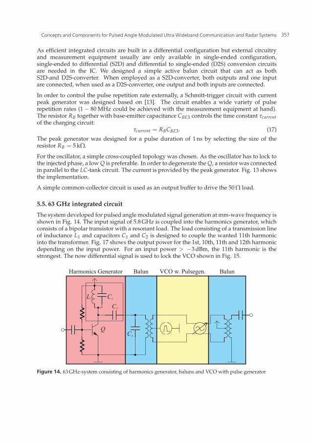
5.5. 63 GHz integrated circuit
The system developed for pulsed angle modulated signal generation at mm-wave frequency isshown in Fig. 14. The input signal of 5.8 GHz is coupled into the harmonics generator, whichconsists of a bipolar transistor with a resonant load. The load consisting of a transmission lineof inductance L1 and capacitors C1 and C2 is designed to couple the wanted 11th harmonicinto the transformer. Fig. 17 shows the output power for the 1st, 10th, 11th and 12th harmonicdepending on the input power. For an input power > −3 dBm, the 11th harmonic is thestrongest. The now differential signal is used to lock the VCO shown in Fig. 15.
Figure 14. 63 GHz-system consisting of harmonics generator, baluns and VCO with pulse generator
357Concepts and Components for Pulsed Angle Modulated Ultra Wideband Communication and Radar Systems
16 UKoLoS
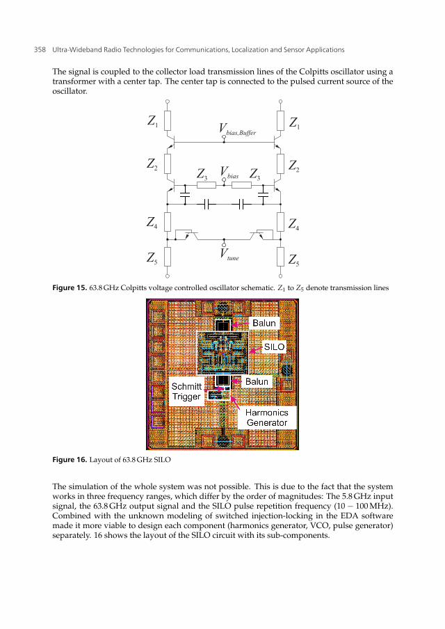
The signal is coupled to the collector load transmission lines of the Colpitts oscillator using atransformer with a center tap. The center tap is connected to the pulsed current source of theoscillator.
Figure 15. 63.8 GHz Colpitts voltage controlled oscillator schematic. Z1 to Z5 denote transmission lines
Figure 16. Layout of 63.8 GHz SILO
The simulation of the whole system was not possible. This is due to the fact that the systemworks in three frequency ranges, which differ by the order of magnitudes: The 5.8 GHz inputsignal, the 63.8 GHz output signal and the SILO pulse repetition frequency (10− 100 MHz).Combined with the unknown modeling of switched injection-locking in the EDA softwaremade it more viable to design each component (harmonics generator, VCO, pulse generator)separately. 16 shows the layout of the SILO circuit with its sub-components.
358 Ultra-Wideband Radio Technologies for Communications, Localization and Sensor Applications

Concepts and Components for Pulsed Angle Modulated Ultra Wideband Communication and Radar Systems 17
Figure 17. Power of the generated harmonics over the input power of the harmonics generator
6. Measurement setup and results
6.1. Verification of sampling theory
In order to verify the theoretical predictions concerning the switched injection lockedharmonic sampling approach according to section 3.3, a demonstrator based on lumpedplanar components was built (see Fig. 18 and 19). It consists of a 480 MHz, 0 dBm signalsource, a 10 MHz DAC modulated phase shifter, a single biased bipolar transistor frequencymultiplier, a band pass filter (200 MHz @ 5.8 GHz) and the 5.8 GHz switched injectionlocked oscillator, which is turned on and off by the digital baseband synchronously to DACmodulation. Fig. 20 depicts the spectrum at the SILO’s output. It features the typical sincshaped peak comb in pulsed mode, which is aligned to and follows the injection frequency of5.76 GHz when changed. When tuning the oscillators natural frequency (which is accordingto Fig. (20) different from the injection frequency) using a varactor diode, the sinc shape of thespectrum moves on the frequency axis while the peak positions do not change. These resultsprove most of the main claims of the generalized sampling theory according to (5) [4].
Figure 18. Implementation of communication and radar signal generator [4]
359Concepts and Components for Pulsed Angle Modulated Ultra Wideband Communication and Radar Systems

18 UKoLoS
Figure 19. Hardware components for the 6 GHz transmitter system demonstrator (using lumped planarcomponents SILO implementation)
5.2 5.4 5.6 5.8 6 6.2 6.4−80
−70
−60
−50
−40
frequency in GHz
pow
er in
dB
m
5.76 5.78 5.8 5.82 5.84−80
−60
−40
−20
0
frequency in GHz
pow
er in
dB
m
pulsedCW
Figure 20. Spectrum of SILO based demonstrator with CW modulation; large peak: oscillatorpermanently on, comb: pulsed oscillator, background: comb zoomed out to show envelope, span 1.5GHz [4]
360 Ultra-Wideband Radio Technologies for Communications, Localization and Sensor Applications

Concepts and Components for Pulsed Angle Modulated Ultra Wideband Communication and Radar Systems 19
6.2. Synthesis of communication signals
The synthesis of time domain communication signals was demonstrated using an 8 PSKmodulation with cyclic transmission of all symbol values and maximum symbol rate, i.e. onesymbol per pulse. The output signal of the demonstrator (Fig. 18, 19) was mixed to basebandusing a quadrature mixer and displayed using an oscilloscope. Its waveform (Fig. 21) clearlyshows the phase states and their repeatability in the IQ diagram. These results prove for thefirst time that it is feasible to generate UWB signals with more complex phase modulationthan BPSK while at the same time keeping complexity and power consumption low.
0 0.2 0.4 0.6 0.8 1 1.2 1.4 1.6 1.8 2−0.3−0.2−0.1
00.10.20.3
time in us
ampl
itude
in V
inphase component (I)
0 0.2 0.4 0.6 0.8 1 1.2 1.4 1.6 1.8 2−0.3
−0.2
−0.1
0
0.1
0.2
0.3
time in us
ampl
itude
in V
quadrature component (Q)
−0.4 −0.3 −0.2 −0.1 0 0.1 0.2 0.3 0.4−0.4
−0.3
−0.2
−0.1
0
0.1
0.2
0.3
0.4
inphase amplitude in V
quad
ratu
re a
mpl
itude
in V
time domain waveform in IQ plane
Figure 21. Generator output with 8 PSK modulation mixed to DC; left: inphase and quadraturecomponent, right: IQ diagram [4]
6.3. Synthesis of radar signals
According to sections 3.5 and 4.3, the same simple hardware implementation used forcommunication signal synthesis (Fig. (18), (19)) can be employed to generate pulsed frequencymodulated radar signals by repeatedly transmitting a limited list of phase samples. For a pulserate of 10 MHz and a ramp slope of 20 MHz/μs, only 50 phase samples (one per pulse) aresufficient.
Figure 22. Measurement setup (on-waver) for the synthesis of radar signals using an integrated circuitSILO [3]
361Concepts and Components for Pulsed Angle Modulated Ultra Wideband Communication and Radar Systems

20 UKoLoS
0 2 4 6 8 10
x 107
−30
−25
−20
−15
−10
−5
0
5
10FMCW beat spectrum (upsweep)
frequency in Hz
rela
tive
pow
er in
dB
1ns pulse
Figure 23. Beat spectrum (6-8 GHz SILO chip) of measured radar signal after mixing with linear sweepand before low pass filtering [3]
1.89 1.9 1.91 1.92 1.93 1.94 1.95 1.96 1.97
x 106
−50
−40
−30
−20
−10
0
10FMCW beat spectrum (upsweep)
frequency in Hz
rela
tive
pow
er in
dB
1ns pulse1ns pulse, 1m extra cable
Figure 24. Zoomed beat spectrum (6-8 GHz SILO chip), comparison of two waveforms with differenttransmission delays [3]
362 Ultra-Wideband Radio Technologies for Communications, Localization and Sensor Applications

Concepts and Components for Pulsed Angle Modulated Ultra Wideband Communication and Radar Systems 21
1.009 1.01 1.011 1.012 1.013 1.014 1.015 1.016
x 107
−50
−40
−30
−20
−10
0
10FMCW beat spectrum (downsweep)
frequency in Hz
rela
tive
pow
er in
dB
5ns pulse7.5ns pulse10ns pulse5ns pulse, 1m extra cable7.5ns pulse, 1m extra cable10ns pulse, 1m extra cable
Figure 25. Comparison of 6-8 GHz chip (2 GHz bandwidth) with lumped implementation (widerpulses, smaller bandwidth) [3]
For verification, this approach was realized both using the previously employed lumpedcomponents SILO (6 GHz, 600 MHz bandwidth) and the first large bandwidth integratedcircuit implementations (7 GHz, >2 GHz bandwidth) in order to demonstrate the resolutionbenefit for ranging. The setup for both experiments is depicted in Fig. 22; the generatedand delayed signal is acquired using an oscilloscope and evaluated on a PC using a numericalcomputation software where it is mixed with a linear FMCW signal and analyzed in frequencydomain (FFT).
Fig. 23 and 24 show the resulting beat frequency spectrum for the integrated circuitimplementation using 1 ns pulses and 10 MHz pulse repetition rate. It corresponds to equation(10) except the small peaks that result from imperfections in the oscillator design leading to aslight turn-on pulse self-locking effect. Future designs are expected to fix this issue.
Comparing the results of the lumped and integrated circuit implementations (see Fig. 25), thebenefit of much higher bandwidths regarding resolution becomes obvious. If the oscillator’sspectral bandwidth is too small in relation to the sweep bandwidth, the beat frequency peakis broadened because of additional windowing through the narrowband SILO spectrum.Therefore, the oscillator bandwidth / pulse width should be adjusted to the desired sweepbandwidth in order to maximize spectral efficiency [3].
6.4. VCO with switch IC
The manufactured circuit is depicted in Fig.26. It measures 710× 1455 μm². For reasons ofnonavailability of differential equipment, all measurements were done single-ended with theunused output terminated to ground with a 50 Ω resistor.
Fig. 27 shows the output power over the tuning range. The 10 dB decrease of output powercompared to the previously published [8] VCO is attributed to the different VCO output bufferand the insertion loss of the switch.
363Concepts and Components for Pulsed Angle Modulated Ultra Wideband Communication and Radar Systems

22 UKoLoS
Figure 26. VCO with switch circuit IC photograph
Figure 27. Measured output power of 1st, 2nd and 3rd harmonic of VCO with switch
The phase noise performance of the VCO with switch has deteriorated significantly from theprevious [8] stand-alone VCO. This is mainly attributed to the new buffer structure whichperformed worse than anticipated.
6.5. 7 GHz SILO IC
The IHP Technologies SGB25V 250 nm SiGe:C BiCMOS process was chosen formanufacturing. It provides a cheap and flexible platform including one or two thick topmetal layers consisting of aluminum. The advantage of using a BiCMOS process for atransmitter circuit is the possibility to build a system-on-a-chip (SoC) solution that integrates
364 Ultra-Wideband Radio Technologies for Communications, Localization and Sensor Applications

Concepts and Components for Pulsed Angle Modulated Ultra Wideband Communication and Radar Systems 23
Figure 28. Measured phase noise of VCO with switch circuit
Figure 29. Manufactured 7 GHz SILO IC
digital baseband and analog RF circuits. Fig. 29 shows a chip photograph with connectedmeasurement probes.
Fig. 30 shows the output power spectrum of the manufactured SILO.
The 10 dB-bandwidth stretches from 5to 8 GHz. A single pulse is shown in Fig. 31. A singlecycle of oscillator start up, oscillation and decay has a duration of 1.5 ns.
365Concepts and Components for Pulsed Angle Modulated Ultra Wideband Communication and Radar Systems

24 UKoLoS
4 5 6 7 8 9 10
x 109
−100
−95
−90
−85
−80
−75
−70
−65
−60
−55
−50
frequency in Hz
pow
er le
vel i
n dB
m
Figure 30. Measured output spectrum of 7 GHz SILO IC
0 0.5 1 1.5 2 2.5 3 3.5−0.1
−0.05
0
0.05
0.1
0.15
time in ns
ampl
itude
in V
Figure 31. Transient output of 7 GHz SILO IC
7. Future work
Since this project is still ongoing, future work will cover further aspects that enhance theoryand hardware implementation. Regarding pulsed angle modulated signals, more complexmodulation schemes will be developed in conjunction with a more comprehensive study oferror sources and their compensation. Furthermore, the first designs of the SILO circuit will
366 Ultra-Wideband Radio Technologies for Communications, Localization and Sensor Applications

Concepts and Components for Pulsed Angle Modulated Ultra Wideband Communication and Radar Systems 25
be refined for an even better performance and higher integration level. Last but not least,hardware concepts for receiver technology are being developed.
Acknowledgement
This work was supported by the German Research Foundation (DFG - priority programSPP1202, grant VO 1453/3-2) within the project “Components and concepts for low-powermm-wave pulsed angle modulated ultra wideband communication and ranging”.
Author details
Alexander Esswein and Robert WeigelInstitute for Electronics Engineering, University of Erlangen-Nuremberg, Germany
Christian Carlowitz and Martin VossiekInstitute of Microwaves and Photonics, University of Erlangen-Nuremberg, Germany
8. References
[1] Barrett, T. W. [2000]. History of UltraWideBand (UWB) Radar & Communications:Pioneers and Innovators.
[2] Carlowitz, C., Esswein, A., Weigel, R. & Vossiek, M. [2012a]. A low power PulseFrequency Modulated UWB radar transmitter concept based on switched injectionlocked harmonic sampling, Microwave Conference (GeMiC), 2012 The 7th German, pp. 1–4.
[3] Carlowitz, C., Esswein, A., Weigel, R. & Vossiek, M. [2012b]. Synthesis of PulsedFrequency Modulated Ultra Wideband Radar Signals Based on Stepped Phase Shifting,IEEE International Conference on Ultra-Wideband (ICUWB) .
[4] Carlowitz, C. & Vossiek, M. [2012]. Synthesis of Angle Modulated Ultra WidebandSignals Based on Regenerative Sampling, IEEE International Microwave Symposium 2012.
[5] Chandrakasan, A., Lee, F., Wentzloff, D., Sze, V., Ginsburg, B., Mercier, P., Daly, D. &Blazquez, R. [2009]. Low-Power Impulse UWB Architectures and Circuits, Proceedings ofthe IEEE 97(2): 332–352.
[6] Deparis, N., Loyez, C., Rolland, N. & Rolland, P.-A. [2008]. UWB in Millimeter WaveBand With Pulsed ILO, Circuits and Systems II: Express Briefs, IEEE Transactions on55(4): 339 –343.
[7] Deparis, N., Siligarisy, A., Vincent, P. & Rolland, N. [2009]. A 2 pJ/bit pulsed ILO UWBtransmitter at 60 GHz in 65-nm CMOS-SOI, Ultra-Wideband, 2009. ICUWB 2009. IEEEInternational Conference on, pp. 113 –117.
[8] Esswein, A., Dehm-Andone, G., Weigel, R., Aleksieieva, A. & Vossiek, M. [2010]. A lowphase-noise SiGe Colpitts VCO with wide tuning range for UWB applications, WirelessTechnology Conference (EuWIT), 2010 European, pp. 229 –232.
[9] Grass, E., Siaud, I., Glisic, S., Ehrig, M., Sun, Y., Lehmann, J., Hamon, M., Ulmer-Moll,A., Pagani, P., Kraemer, R. & Scheytt, C. [2008]. Asymmetric dual-band UWB / 60 GHzdemonstrator, Personal, Indoor and Mobile Radio Communications, 2008. PIMRC 2008. IEEE19th International Symposium on, pp. 1 –6.
[10] Hancock, T. & Rebeiz, G. [2005]. Design and Analysis of a 70-ps SiGe Differential RFSwitch, Microwave Theory and Techniques, IEEE Transactions on 53(7): 2403 – 2410.
367Concepts and Components for Pulsed Angle Modulated Ultra Wideband Communication and Radar Systems

26 UKoLoS
[11] J. Ryckaert et al [2006]. A 16mA UWB 3-to-5GHz 20Mpulses/s Quadrature AnalogCorrelation Receiver in 0.18/spl mu/m CMOS, Solid-State Circuits Conference, 2006.ISSCC 2006. Digest of Technical Papers. IEEE International, pp. 368 –377.
[12] Kohno, R. [2008]. Latest regulation and R&D for UWB inter-vehicle radar in millimeterwave band, 8th International Conference on ITS Telecommunications, ITST .
[13] Lin, D., Schleicher, B., Trasser, A. & Schumacher, H. [2011]. Si/SiGe HBT UWBimpulse generator tunable to FCC, ECC and Japanese spectral masks, Radio and WirelessSymposium (RWS), 2011 IEEE, pp. 66 –69.
[14] Miesen, R., Ebelt, R., Kirsch, F., Schaefer, T., Li, G., Wang, H. & Vossiek, M. [2011].Where is the Tag? History, Modern Concepts, and Applications of Locatable RFIDs, IEEEMicrowave Magazine . to be published.
[15] Pohl, N., Rein, H.-M., Musch, T., Aufinger, K. & Hausner, J. [2009]. SiGe Bipolar VCOWith Ultra-Wide Tuning Range at 80 GHz Center Frequency, 44(10): 2655–2662.
[16] Roehr, S., Gulden, P. & Vossiek, M. [2008]. Precise Distance and Velocity Measurement forReal Time Locating Using a Frequency Modulated Continuous Wave Secondary RadarApproach, IEEE Transactions on Microwave Theory and Techniques 56(10): 2329–2339.
[17] Sewiolo, B., Hartmann, M., Guenther, O. & Weigel, R. [2006]. System Simulation of a 79GHz UWB-Pulse Radar Transceiver Front-End for Automotive Applications, VDE / ITGDiskussionssitzung Antennen und Messverfahren fuer Ultra-Wide-Band(UWB)-Systeme (UWB2006) Kamp-Lintfort, Germany .
[18] Trotta, S., Dehlink, B., Knapp, H., Aufinger, K., Meister, T., Bock, J., Simburger, W. &Scholtz, A. [2007]. SiGe Circuits for Spread Spectrum Automotive Radar, Ultra-Wideband,2007. ICUWB 2007. IEEE International Conference on, pp. 523 –528.
[19] Vossiek, M. & Gulden, P. [2008]. The Switched Injection-Locked Oscillator: A NovelVersatile Concept for Wireless Transponder and Localization Systems, Microwave Theoryand Techniques, IEEE Transactions on 56(4): 859 –866.
[20] Wentzloff, D. & Chandrakasan, A. [2006]. Gaussian pulse Generators for subbandedultra-wideband transmitters, Microwave Theory and Techniques, IEEE Transactions on54(4): 1647 – 1655.
368 Ultra-Wideband Radio Technologies for Communications, Localization and Sensor Applications