amplitude and angle modulationamplitude and angle modulation29 2.6 power relation in am wave...
TRANSCRIPT
22 Communication Systems
CHAPTER 2
Amplitude and Angle Modulation
2.1 INTRODUCTION
Modulation is the process or result of the process by which a message is changedinto information. Modulation plays vital role in the field of communication.Communication involves the transmission, reception and processing of informationby electrical means. For the propagation of electric signals, the media used iselectromagnetic field and when this field changes with time it takes the form ofwave. Modulation is also the process whereby in response to the received waveeither the original message or information pertaining the original message is madeavailable in the desired form and is delivered when it is wanted. “Demodulationand detection” are the terms often observed to denote the recovery of the wantedmessage from a modulated signal. Modulation is fundamental to communicationand it implies the bandwidth occupancy. In the chapter, we will basically deal withthe fundamental concepts of Amplitude Modulation and Phase Modulation.
2.2 NEED FOR MODULATION
If the signal is send directly, i.e. without modulation, i.e. unmodulated carrierseveral difficulties arise which are listed below:
(1) Antenna height: Theory of antenna tells that for the efficient radiation ofelectromagnetic waves the height of antenna must be comparable to the quarterwavelength of the frequency which we are using.
Now suppose you want to transmit the audio frequency, i.e. 20 kHz, weknow that
C f= λ
Cf
∴λ = (1)
where, λ = wavelength, C = velocity of light, f = frequency
24 Communication Systems
In the process of modulation low frequency bandlimited signal is mixed withhigh frequency wave called, “carrier wave”. Such a carrier wave may be representedby the equation
e = Em sin (ωt + φ) (2)where, e = instantaneous value of sine wave,
Em = maximum amplitude,ω = angular frequency,φ = phase relation with respect to some reference.
Any of these last three characteristics or parameters of the carrier may bevaried by the low frequency modulating signal during the process of modulation.Thus, in the process of modulation, some characteristics of high frequencysinusoidal wave is varied in accordance with the instantaneous value of modulatingsignal since there are three parameters Em, ω and φ of a carrier wave, therefore,any of these parameters can be varied in proportion to the instantaneous value ofthe modulating signal, giving rise to amplitude, frequency or phase modulationrespectively.
Frequency and phase modulation are together named as “angle modulation”,as variation of any of the two varies the angle of the carrier wave.
Amplitude Modulation:In this type of modulation, the amplitude of carrier signal is varied by the modulatingvoltage, whose frequency is less than that of carrier.
Let Vc = Vc sin ωc tand Vm = Vm sin ωm t
in the above expressions, the phase angle has been ignored.
2.3 FREQUENCY SPECTRUM OF AM WAVE
Amplitude modulation is a system of modulation in which the amplitude of thecarrier is made proportional to the instantaneous amplitude of modulating signal.
Sideband frequency is defined asfSB = fc ± n fm (3)
and in the first pair n = 1.When a carrier is amplitude modulated, the proportionality constant is made
equal to unity and the instantaneous modulating voltage variations are superimposedon to the carrier amplitude. Hence, when there is no modulation, the amplitude ofcarrier is equal to its unmodulated value. When modulation is present the amplitudeof the carrier is varied by its instantaneous value. This is shown in Fig. 2.1. In thefigure it is clear that what will happen if Em is greater than Ec.
Modulation index (m) is given by
m
c
EmE
= (4)
26 Communication Systems
cc c c m c m
m EE E sin t [cos( )t cos( )t]2
= ω + ω − ω − ω + ω
c cc c c m c m
m E m EE E sin t cos( )t cos( )t2 2
= ω + ω −ω − ω + ω (7)
where, Ec sin ωc t = Unmodulated carrier
cc m
m E cos( )t2
ω −ω = Lower sideband
cc m
m E cos( )t2
− ω + ω = Upper sideband
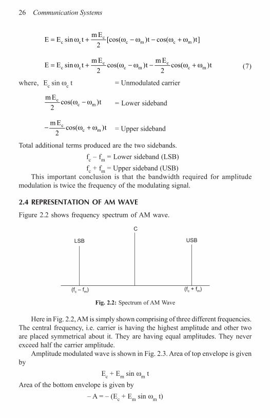
Total additional terms produced are the two sidebands.fc – fm = Lower sideband (LSB)fc + fm = Upper sideband (USB)
This important conclusion is that the bandwidth required for amplitudemodulation is twice the frequency of the modulating signal.
2.4 REPRESENTATION OF AM WAVE
Figure 2.2 shows frequency spectrum of AM wave.
LSB
C
USB
(f – f )c m(f + f )c m
Fig. 2.2: Spectrum of AM Wave
Here in Fig. 2.2, AM is simply shown comprising of three different frequencies.The central frequency, i.e. carrier is having the highest amplitude and other twoare placed symmetrical about it. They are having equal amplitudes. They neverexceed half the carrier amplitude.
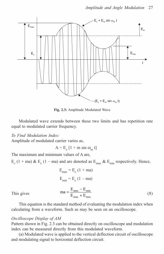
Amplitude modulated wave is shown in Fig. 2.3. Area of top envelope is givenby
Ec + Em sin ωm tArea of the bottom envelope is given by
– A = – (Ec + Em sin ωm t)
Amplitude and Angle Modulation 27
Modulated wave extends between these two limits and has repetition rateequal to modulated carrier frequency.
To Find Modulation Index:Amplitude of modulated carrier varies as,
A = Ec [1 + m sin ωm t]The maximum and minimum values of A are,Ec (1 + ma) & Ec (1 – ma) and are denoted as Emax & Emin respectively. Hence,
Emax = Ec (1 + ma)
Emin = Ec (1 – ma)
This givesmax min
max min
E Ema
E E−
=+ (8)
This equation is the standard method of evaluating the modulation index whencalculating from a waveform. Such as may be seen on an oscilloscope.
Oscilloscope Display of AMPattern shown in Fig. 2.3 can be obtained directly on oscilloscope and modulationindex can be measured directly from this modulated waveform.
(a) Modulated wave is applied to the vertical deflection circuit of oscilloscopeand modulating signal to horizontal deflection circuit.
Fig. 2.3: Amplitude Modulated Wave
Emin
E + E sin tc m m
Em
Emax
Ec
– (E + E sin t)c m m
t
Amplitude and Angle Modulation 29
2.6 POWER RELATION IN AM WAVE
Modulated wave contains more power than the carrier had before modulation tookplace. Since the amplitude of the side bands depends on the modulation index, it isanticipated that the total power in the modulated wave will depend on the modulationindex also.
The total power in the modulated wave will be
2 2 2carrier LSB USB
tE E EP
R R R= + + (9)
where, all three voltages are rms values & R is the resistance in which power isdissipated.
2carrier
2 2carrier c
c
EE E2P
R R 2R
∴ = = = (10)
2c
2 2c
LSB USB
m Em E2P P / R
2 8R
= = =
2 2 2 2c cm E E m
8R 2R 4= = (11)
∴ Putting values of equations (11) & (10) in equation (9)
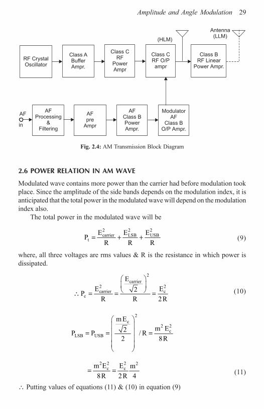
Fig. 2.4: AM Transmission Block Diagram
RF CrystalOscillator
Class ABufferAmpr.
Class CRF
PowerAmpr
(HLM)
Class CRF O/Pampr
Class BRF Linear
Power Ampr.
Antenna(LLM)
AF
in
AFProcessing
&Filtering
AFpre
Ampr
AFClass BPowerAmpr.
ModulatorAF
Class BO/P Ampr.
30 Communication Systems
2 2 2carr LSB USB
tE E EP
R R R= + +
2 2 22 2c c c
tE E Em mP2R 2R 4 2R 4
∴ = + +
2 2 2 22 2 2c c c cE E E Em m m
2R 2R 4 4 2R 2R 2
= + + = +
2 2c
tE mP 12R 2
= +
but Pc = carrier power = 2cE
2R
2
t cmP P 12
∴ = +
(12)
Example 2.1: A broadcast AM transmitter radiates 50 kW of carrier power whatwill be radiated power at 85% modulation?
GivenPc = 50 kW
Percentage modulation = 85To find : Pt = total power radiated.
Solution:2
t cmP P 12
= +
2(0.85)50 kW 12
= +
= 68.06 kW.
Example 2.2: A broadcast radio transmitter radiates 10 kW when the modulationpercentage is 60. How much of this is carrier power?
Solution: t aP 10 kW, m 60%= =
32 Communication Systems
∴7
cc
6.28 10f 10 MHz2 2ω ×= = =π π
fc = 10 MHz
(b) Modulating frequency:m
m3140f 500 Hz
2 2ω= = =π π
(c) Carrier power:2 2c
cE 500P 208.33 W2R 2 600
= = =×
(d) Mean power output:
2 2a
t cm 2500 0.4 2500P P 1 1 1.082 12 2 12
= + = + = ×
Pt = 225 watts
(e) Peak power output results when the positive half cycle of the modulatingsignal occurs. The peak output voltage is given by the sum of Ec & Em:
Peak output voltage = Ec + m Ec = 500 + 0.4 × 500Peak output voltage = 700 V
tm700 700 1Peak power P
6002 2= = × ×
Ptm = 408.3 watts
2.7 CURRENT CALCULATIONS FOR AM WAVE
Sometimes it is easy to measure RF currents instead of voltages. We analyze sucha situation in this section.Let Ic be rms unmodulated current.
It = Total rms modulated current of AM transmitter.R = Resistance in which the above two currents flow. Then,
2 2t t t
2 2c c c
P I R IP I R I
= =
but2
t a
c
P m1P 2
= +

Amplitude and Angle Modulation 35
2.10 NON-LINEAR MODULATION
In general, any device operated in non-linear region of its output characteristics iscapable of producing amplitude modulated waves when the carrier and modulatingsignals are fed at the input. Thus, a transistor, a triode tube, a diode, etc. may beused as Square Law modulator. In such a modulator circuit, the output currentflowing through the load is given by the power series
i = a0 + a1 e1 + a2 e12 + …
where, a0, a1, a2, etc. are constant and e1 is the input voltage to the device.Considering the modulator circuit of Fig. 2.5
e1 = Ec sin ωc t + Em sin ωm t
i = a0 + a1 (Ec sin ωc t + Em sin ωm t) +
a2 (Ec sin ωc t + Em sin ωm t)2
= a0 + a1 Ec sin ωc t + a1 Em sin ωm t + a2 Ec2 sin2 ωc t
+ a2 Em2 sin2 ωm t + 2 Ec Em sin ωc t sin ωm t
= a0 + a1 Ec sin ωc t + a1 Em sin ωm t + a2 Em2 sin2 ωm t + a2 Ec
2 sin2 ωc t
+ c 2 m2E a E2 [cos (ωc – ωm) t – cos (ω + ωm) t]
i = a0 + a1 Ec sin ωc t + a1 Em sin ωm t + a2 Ec2 sin2 ωc t
+ a2 Em2 sin2 ωm t + a2 EcEm [cos (ωc – ωm) t – cos (ωc + ωm)t]
The last term of this equation (underlined) gives the upper and lower sidebandswhile the second term gives the carrier. If the load is resonant circuit, sidebandsand carrier may be selected giving the AM output. When all unwanted frequenciesare rejected, the modulated component present at the output is represented by
i = a1 Ec sin ωc t + a2 Ec Em [cos (ωc – ωm) t – cos (ωc + ωm) t]
Fig. 2.5
Non-lineardevice
E sin tcc
E sin tmm
e1
Load
36 Communication Systems
As “a1” is considerably larger than a2, the depth of modulation that is availablewithout distortion is low.
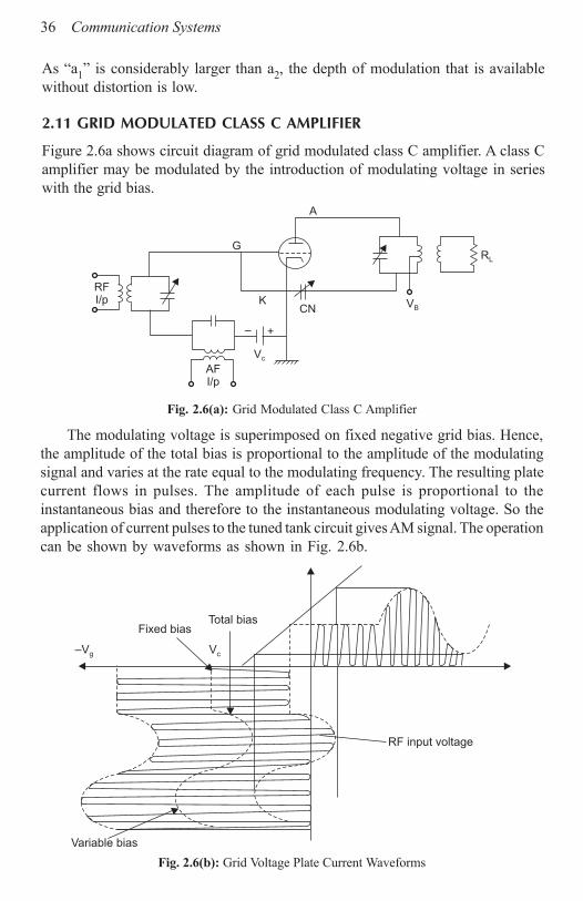
2.11 GRID MODULATED CLASS C AMPLIFIER
Figure 2.6a shows circuit diagram of grid modulated class C amplifier. A class Camplifier may be modulated by the introduction of modulating voltage in serieswith the grid bias.
Total biasFixed bias
–Vg Vc
RF input voltage
Variable bias
Fig. 2.6(b): Grid Voltage Plate Current Waveforms
– +
AFI/p
RFI/p
Vc
CN VB
RL
G
A
K
Fig. 2.6(a): Grid Modulated Class C Amplifier
The modulating voltage is superimposed on fixed negative grid bias. Hence,the amplitude of the total bias is proportional to the amplitude of the modulatingsignal and varies at the rate equal to the modulating frequency. The resulting platecurrent flows in pulses. The amplitude of each pulse is proportional to theinstantaneous bias and therefore to the instantaneous modulating voltage. So theapplication of current pulses to the tuned tank circuit gives AM signal. The operationcan be shown by waveforms as shown in Fig. 2.6b.
Amplitude and Angle Modulation 37
This system will operate without distortion or have undistorted output only ifthe transfer characteristic of triode is perfectly linear. Because this can never beso, the output must be somewhat distorted.
Due to such bias conditions, the maximum output power from a grid modulatedamplifier is very less than that would be obtained from the same tube if it isunmodulated. The disadvantages of grid modulation are counterbalanced by thelower modulating power needed in comparison with plate modulation. Harmonicsgenerated due to non-linearity of transfer characteristics are reduced by operatingamplifier in push pull.
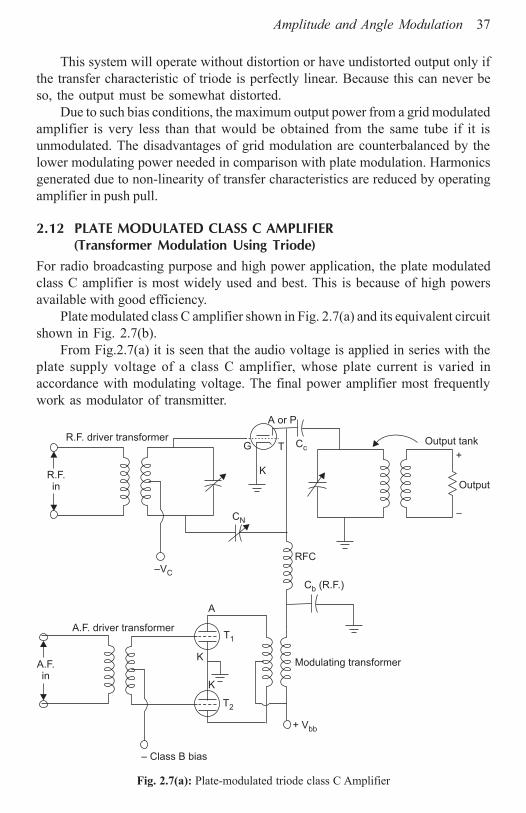
2.12 PLATE MODULATED CLASS C AMPLIFIER
(Transformer Modulation Using Triode)
For radio broadcasting purpose and high power application, the plate modulatedclass C amplifier is most widely used and best. This is because of high powersavailable with good efficiency.
Plate modulated class C amplifier shown in Fig. 2.7(a) and its equivalent circuitshown in Fig. 2.7(b).
From Fig.2.7(a) it is seen that the audio voltage is applied in series with theplate supply voltage of a class C amplifier, whose plate current is varied inaccordance with modulating voltage. The final power amplifier most frequentlywork as modulator of transmitter.
R.F.in
A.F.in
R.F. driver transformerG T Cc
Output tank
+
–
Output
K
CN
–VC
RFC
C (R.F.)b
A.F. driver transformer
K
T2
+ Vbb
– Class B bias
A or P
Modulating transformer
A
T1
K
Fig. 2.7(a): Plate-modulated triode class C Amplifier
38 Communication Systems
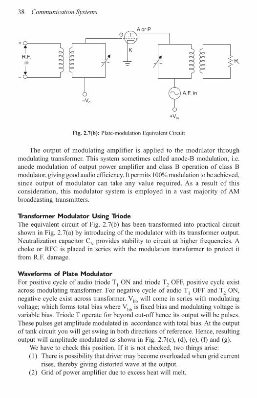
The output of modulating amplifier is applied to the modulator throughmodulating transformer. This system sometimes called anode-B modulation, i.e.anode modulation of output power amplifier and class B operation of class Bmodulator, giving good audio efficiency. It permits 100% modulation to be achieved,since output of modulator can take any value required. As a result of thisconsideration, this modulator system is employed in a vast majority of AMbroadcasting transmitters.
Transformer Modulator Using Triode
The equivalent circuit of Fig. 2.7(b) has been transformed into practical circuitshown in Fig. 2.7(a) by introducing of the modulator with its transformer output.Neutralization capacitor CN provides stability to circuit at higher frequencies. Achoke or RFC is placed in series with the modulation transformer to protect itfrom R.F. damage.
Waveforms of Plate Modulator
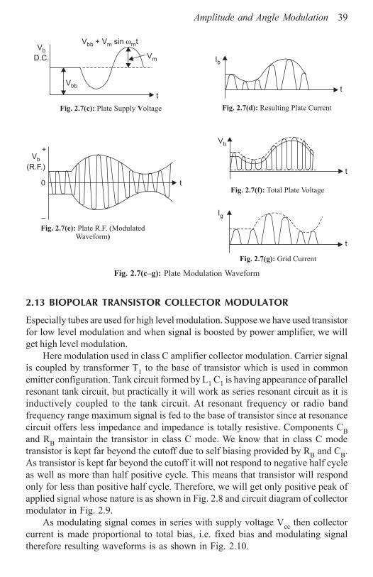
For positive cycle of audio triode T1 ON and triode T2 OFF, positive cycle existacross modulating transformer. For negative cycle of audio T1 OFF and T2 ON,negative cycle exist across transformer. Vbb will come in series with modulatingvoltage; which forms total bias where Vbb is fixed bias and modulating voltage isvariable bias. Triode T operate for beyond cut-off hence its output will be pulses.These pulses get amplitude modulated in accordance with total bias. At the outputof tank circuit you will get swing in both directions of reference. Hence, resultingoutput will amplitude modulated as shown in Fig. 2.7(c), (d), (e), (f) and (g).
We have to check this position. If it is not checked, two things arise:(1) There is possibility that driver may become overloaded when grid current
rises, thereby giving distorted wave at the output.(2) Grid of power amplifier due to excess heat will melt.
R.F.in
–VC
A.F. in
RL
K
GA or P
+Vbb
+
–
Fig. 2.7(b): Plate-modulation Equivalent Circuit
Amplitude and Angle Modulation 39
V + V sinbb m mt
Vm
Vbb
t
V
D.C.b
t
t
Fig. 2.7(c): VPlate Supply oltage Fig. 2.7(d): Resulting Plate Current
Fig. 2.7(e):)
Plate R.F. (ModulatedWaveform
Fig. 2.7(f): Total Plate Voltage
Fig. 2.7(g): Grid Current
Ib
+
–
V
(R.F.)b
Vb
Ig
t
t
0
2.13 BIOPOLAR TRANSISTOR COLLECTOR MODULATOR
Especially tubes are used for high level modulation. Suppose we have used transistorfor low level modulation and when signal is boosted by power amplifier, we willget high level modulation.
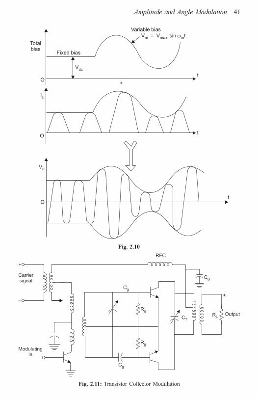
Here modulation used in class C amplifier collector modulation. Carrier signalis coupled by transformer T1 to the base of transistor which is used in commonemitter configuration. Tank circuit formed by L1 C1 is having appearance of parallelresonant tank circuit, but practically it will work as series resonant circuit as it isinductively coupled to the tank circuit. At resonant frequency or radio bandfrequency range maximum signal is fed to the base of transistor since at resonancecircuit offers less impedance and impedance is totally resistive. Components CBand RB maintain the transistor in class C mode. We know that in class C modetransistor is kept far beyond the cutoff due to self biasing provided by RB and CB.As transistor is kept far beyond the cutoff it will not respond to negative half cycleas well as more than half positive cycle. This means that transistor will respondonly for less than positive half cycle. Therefore, we will get only positive peak ofapplied signal whose nature is as shown in Fig. 2.8 and circuit diagram of collectormodulator in Fig. 2.9.
As modulating signal comes in series with supply voltage Vcc then collectorcurrent is made proportional to total bias, i.e. fixed bias and modulating signaltherefore resulting waveforms is as shown in Fig. 2.10.
Fig. 2.7(c–g): Plate Modulation Waveform
Amplitude and Angle Modulation 41
Fig. 2.10
Vdc
Totalbias
Fixed bias
Variable bias
Vm Vmax= sin tm
Ic
Ot
+
tO
Ot
Vo
Fig. 2.11: Transistor Collector Modulation
CB
RLCT
Cg
Rg
Rg
Cg
RFC
Carriersignal
Modulatingin
Output
+
–
+
–
42 Communication Systems
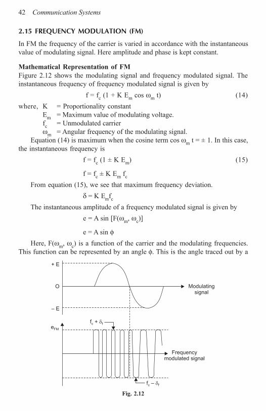
2.15 FREQUENCY MODULATION (FM)
In FM the frequency of the carrier is varied in accordance with the instantaneousvalue of modulating signal. Here amplitude and phase is kept constant.
Mathematical Representation of FMFigure 2.12 shows the modulating signal and frequency modulated signal. Theinstantaneous frequency of frequency modulated signal is given by
f = fc (1 + K Em cos ωm t) (14)where, K = Proportionality constant
Em = Maximum value of modulating voltage.fc = Unmodulated carrierωm = Angular frequency of the modulating signal.
Equation (14) is maximum when the cosine term cos ωm t = ± 1. In this case,the instantaneous frequency is
f = fc (1 ± K Em) (15)
f = fc ± K Em fc
From equation (15), we see that maximum frequency deviation.δ = K Emfc
The instantaneous amplitude of a frequency modulated signal is given bye = A sin [F(ωm, ωc)]
e = A sin φHere, F(ωm, ωc) is a function of the carrier and the modulating frequencies.
This function can be represented by an angle φ. This is the angle traced out by a
Fig. 2.12
+ E
O
– E
Modulatingsignal
Frequencymodulated signal
f + fc
f fc –
eFM
Amplitude and Angle Modulation 43
vector A in time t. If we assume that this vector rotates at a constant speed of p,then angle φ would be pt radians. In fact, the speed of this vector is not constantand is dependent on equation (14), i.e.
ω = ωc(1 + K Em cos ωm t)To calculate the value of φ; we integrate ω with respect to time. Thus,
c m mdt (1 K E cos t)dtφ = ω = ω + ω∫ ∫
c m m(1 K E cos t)dt= ω + ω∫
m mc
m
K E sin tt ω= ω + ω
m mc
m
K E sin tt ω= ω +ω
m cc m
m
K E ft sin t
f= ω + ω
c mm
t sin tfδφ = ω + ω
c f mt m sin tφ = ω + ω
where mf = modulation index
m
Maximum deviationf Modulating frequencyδ= =
∴ Instantaneous voltage of FM
eFM = A sin φ
eFM = A sin [ωc t + mf sin ωm t]A point to be noted here is that as the modulating frequency is decreased,
while the modulating voltage amplitude is kept constant, the modulation index mfincreases. This is the basis of distinguishing frequency modulation from phasemodulation.
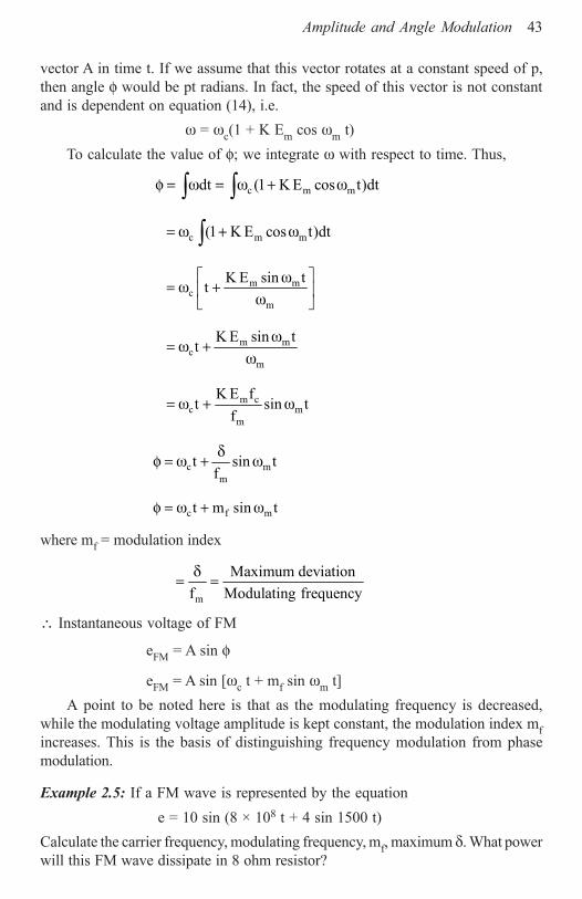
Example 2.5: If a FM wave is represented by the equatione = 10 sin (8 × 10⁸ t + 4 sin 1500 t)
Calculate the carrier frequency, modulating frequency, mf, maximum δ. What powerwill this FM wave dissipate in 8 ohm resistor?
Amplitude and Angle Modulation 45
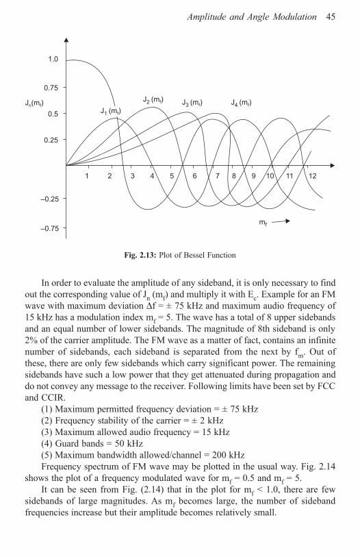
Fig. 2.13: Plot of Bessel Function
1.0
0.75
0.5
0.25
–0.25
–0.75mf
J (m )2 f J (m )3 f J (m )4 f
1 2 3 4 5 6 7 8 9 10 11 12
J (m )1 f
J (m )n f
In order to evaluate the amplitude of any sideband, it is only necessary to findout the corresponding value of Jn (mf) and multiply it with Ec. Example for an FMwave with maximum deviation ∆f = ± 75 kHz and maximum audio frequency of15 kHz has a modulation index mf = 5. The wave has a total of 8 upper sidebandsand an equal number of lower sidebands. The magnitude of 8th sideband is only2% of the carrier amplitude. The FM wave as a matter of fact, contains an infinitenumber of sidebands, each sideband is separated from the next by fm. Out ofthese, there are only few sidebands which carry significant power. The remainingsidebands have such a low power that they get attenuated during propagation anddo not convey any message to the receiver. Following limits have been set by FCCand CCIR.
(1) Maximum permitted frequency deviation = ± 75 kHz(2) Frequency stability of the carrier = ± 2 kHz(3) Maximum allowed audio frequency = 15 kHz(4) Guard bands = 50 kHz(5) Maximum bandwidth allowed/channel = 200 kHzFrequency spectrum of FM wave may be plotted in the usual way. Fig. 2.14
shows the plot of a frequency modulated wave for mf = 0.5 and mf = 5.It can be seen from Fig. (2.14) that in the plot for mf < 1.0, there are few
sidebands of large magnitudes. As mf becomes large, the number of sidebandfrequencies increase but their amplitude becomes relatively small.
Amplitude and Angle Modulation 47
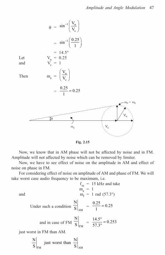
φ =1 n
c
VsinV
−
=1 0.25sin
1−
= 14.5°Let Vn = 0.25and Vc = 1
Then ma =n
c
VV
=0.25 0.25
1=
Vn
Vc
n c–
c
Fig. 2.15
Now, we know that in AM phase will not be affected by noise and in FM.Amplitude will not affected by noise which can be removed by limiter.
Now, we have to see effect of noise on the amplitude in AM and effect ofnoise on phase in FM.
For considering effect of noise on amplitude of AM and phase of FM. We willtake worst case audio frequency to be maximum, i.e.
fm = 15 kHz and takema = 1
and mf = 1 rad (57.3°)
Under such a condition AM
NS =
0.25 0.251
=
and in case of FM FM
NS =
14.5 0.25357.3
° =°
just worst in FM than AM.
FM AM
N Njust worst thanS S
48 Communication Systems
Now suppose audio frequency is reduced from 15 kHz to 30 Hz in audio band.
Then in case of AM there is no effect on NS ratio. In FM
n
c
VV
remains the
constant but noise phase modulate the carrier signal. As audio frequency goes onreducing modulation index goes on increasing when noise and audio signal bothhaving frequency equal to 30 Hz. Then N/S ratio is equal to
0.253 30 0.000505.15,000
× =
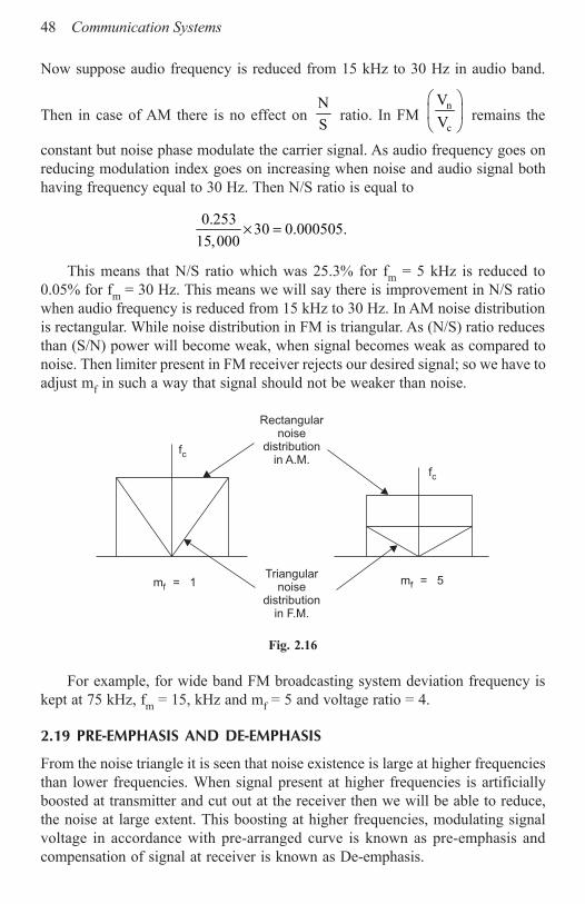
This means that N/S ratio which was 25.3% for fm = 5 kHz is reduced to0.05% for fm = 30 Hz. This means we will say there is improvement in N/S ratiowhen audio frequency is reduced from 15 kHz to 30 Hz. In AM noise distributionis rectangular. While noise distribution in FM is triangular. As (N/S) ratio reducesthan (S/N) power will become weak, when signal becomes weak as compared tonoise. Then limiter present in FM receiver rejects our desired signal; so we have toadjust mf in such a way that signal should not be weaker than noise.
fc
fm = 5
fc
fm = 1
Rectangularnoise
distributionin A.M.
Triangularnoise
distributionin F.M.
Fig. 2.16
For example, for wide band FM broadcasting system deviation frequency iskept at 75 kHz, fm = 15, kHz and mf = 5 and voltage ratio = 4.
2.19 PRE-EMPHASIS AND DE-EMPHASIS
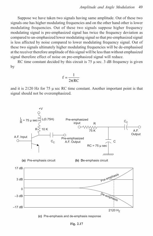
From the noise triangle it is seen that noise existence is large at higher frequenciesthan lower frequencies. When signal present at higher frequencies is artificiallyboosted at transmitter and cut out at the receiver then we will be able to reduce,the noise at large extent. This boosting at higher frequencies, modulating signalvoltage in accordance with pre-arranged curve is known as pre-emphasis andcompensation of signal at receiver is known as De-emphasis.
Amplitude and Angle Modulation 49
Suppose we have taken two signals having same amplitude. Out of these twosignals one has higher modulating frequencies and on the other hand other is lowermodulating frequencies. Out of these two signals suppose higher frequencymodulating signal is pre-emphasized signal has twice the frequency deviation ascompared to un-emphasized lower modulating signal so that pre-emphasized signalis less affected by noise compared to lower modulating frequency signal. Out ofthese two signals ultimately higher modulating frequencies will be de-emphasisedat the receiver therefore amplitude of this signal will be less than without emphasizedsignal therefore effect of noise on pre-emphasized signal will reduce.
RC time constant decided by this circuit is 75 µ sec. 3 dB frequency is givenby
1f2 RC
=π
and it is 2120 Hz for 75 µ sec RC time constant. Another important point is thatsignal should not be overemphasized.
Fig. 2.17
Pre-emphasis
De-emphasis
2120 HZ
(c) Pre-emphasis and de-emphasis response
17 dB
3 dB
0
–3 dB
–17 dB
(a) Pre-emphasis circuit (b) De-emphasis circuit
RCC
75 K A.F.Output
C
RC = 75 µ sec
Pre-emphasizedinput
Pre-emphasizedA.F. Output
A.F. Input
CC
R 10 K
L(0.75H)
+V
LR
= 75 µ sec
Amplitude and Angle Modulation 51
Fig. 2.18
AMtransmitter
(1)
AMReceiver
AMtransmitter
(2)
d < d1 2
d1 d2
FMtransmitter
(1)
FMReceiver
FMtransmitter
(2)
d = d1 2
d1 d2
FMtransmitter
(1)
FMtransmitter
(1)
FMReceiver
FMReceiver
FMtransmitter
(2)
FMtransmitter
(2)
d1
d1
d2
d2
d > d1 2
d < d1 2
Fig. 2.18(a)
Fig. 2.18(b)
Fig. 2.18(c)
Fig. 2.18(d)

52 Communication Systems
2.22.1 Reactance Modulator
Consider a basic reactance modulator shown in Fig. (2.19). It uses FET andbehaves as a three terminal reactance that may be connected a cross a tank circuitof the oscillator to be frequency modulated.
C
R
K
K
i2 i1
Gate
Drain
Z e
Sourceeg
Fig. 2.19: Basic Reactance Modulator
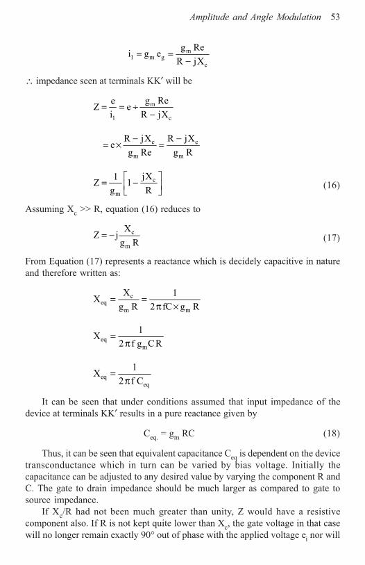
Under certain conditions the impedance “Z” between terminals KK′ becomesentirely reactive. It can be capacitive or inductive by just interchanging onecomponent. The value of the reactance Z is proportional to the transconductanceof the device, which is turn depends upon the gate bias and its variation. The FETcan be replaced by bipolar transistor or vacuum tube.
Theory: To evaluate the value of Z, a voltage “e” is applied at terminal KK′. Theresulting current i1 is calculated. In order for the impedance to be a pure reactancetwo requirements have to be fulfilled. First is that the bias networked current i2should be negligible as compared to drain current i1. In other words, the impedanceof the bias network should be large enough so that it can be ignored. The secondrequirement is that the drain to gate impedance Xc should be greater than the gateto source impedance R preferably by more than five times. (i.e. XC >> R)
Then eg can be written as
g 2c c
e Ree i R RR jX R jX
= = =− −
gc
ReeR jX
=−
The FET drain current will be:
Amplitude and Angle Modulation 53
m1 m g
c
g Rei g eR jX
= =−
∴ impedance seen at terminals KK′ will be
m
1 c
g ReeZ ei R jX
= = ÷−
c c
m m
R jX R jXe
g Re g R− −
= × =
c
m
jX1Z 1g R
= −
(16)
Assuming Xc >> R, equation (16) reduces to
c
m
XZ j
g R= − (17)
From Equation (17) represents a reactance which is decidely capacitive in natureand therefore written as:
ceq
m m
X 1Xg R 2 fC g R
= =π ×
eqm
1X2 f g CR
=π
eqeq
1X2 f C
=π
It can be seen that under conditions assumed that input impedance of thedevice at terminals KK′ results in a pure reactance given by
Ceq. = gm RC (18)
Thus, it can be seen that equivalent capacitance Ceq is dependent on the devicetransconductance which in turn can be varied by bias voltage. Initially thecapacitance can be adjusted to any desired value by varying the component R andC. The gate to drain impedance should be much larger as compared to gate tosource impedance.
If Xc/R had not been much greater than unity, Z would have a resistivecomponent also. If R is not kept quite lower than Xc, the gate voltage in that casewill no longer remain exactly 90° out of phase with the applied voltage ei nor will

56 Communication Systems
The diode is back biased to obtain the junction capacitance effect, this reversebias is achieved by the modulating voltage which in turn varies the junctioncapacitance causing the oscillator frequency to vary proportionally.
Disadvantage of varactor diode modulator is that it uses a two terminal device,thus it is used mostly in automatic frequency-control and remote tuning.
2.24 FREQUENCY STABILIZATION OF FREQUENCY MODULATOR
A prime requirement of any transmitter is the stabilization of the carrier frequency.It is necessary that the average or carrier frequency of a frequency modulator bemaintained very nearly constant, even though the instantaneous frequency offrequency modulator varies with the modulating signal. When a reactance modulatoris used, to modulate the carrier, the carrier cannot be crystal controlled. The averagefrequency depends to some extent on the temperature, the device characteristicsand the operating potentials, slight drift in the operating characteristics isaccompanied by an appreciable change in average frequency. This necessitatessetting up of frequency stabilization system in the frequency modulator to maintainthe carrier frequency within the 2 kHz deviation specified by FCC regulations.
Figure 2.22 shows block diagram of typical AFC system for FM transmitter.It uses crystal oscillator and carrier frequency of the FM signal is compared
with it. The reactance modulator works across the tank circuit of LC oscillator,whose output is isolated by a buffer stage. The output of buffer is fed to anamplitude limiter and subsequently to class-C power amplifiers. A small part of thesignals is taken from the limiter output and fed to a mixer in which this signal ismixed with a signal from the crystal oscillator.
RFC
To tank circuitof oscillator
Varactordiode
C (RF)b
- V bias
AFInput
Fig. 2.21: Modulator Using Varactor Diode
58 Communication Systems
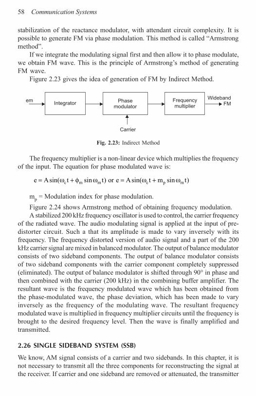
stabilization of the reactance modulator, with attendant circuit complexity. It ispossible to generate FM via phase modulation. This method is called “Armstrongmethod”.
If we integrate the modulating signal first and then allow it to phase modulate,we obtain FM wave. This is the principle of Armstrong’s method of generatingFM wave.
Figure 2.23 gives the idea of generation of FM by Indirect Method.
emIntegrator Phase
modulator
Frequencymultiplier
WidebandFM
Carrier
Fig. 2.23: Indirect Method
The frequency multiplier is a non-linear device which multiplies the frequencyof the input. The equation for phase modulated wave is:
c m m c p me Asin( t sin t) or e Asin( t m sin t)= ω + φ ω = ω + ω
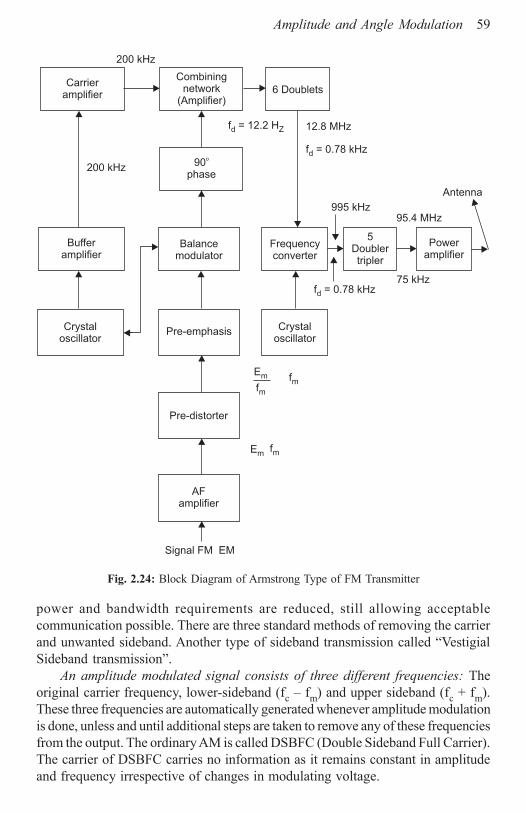
mp = Modulation index for phase modulation.Figure 2.24 shows Armstrong method of obtaining frequency modulation.A stabilized 200 kHz frequency oscillator is used to control, the carrier frequency
of the radiated wave. The audio modulating signal is applied at the input of pre-distorter circuit. Such a that its amplitude is made to vary inversely with itsfrequency. The frequency distorted version of audio signal and a part of the 200kHz carrier signal are mixed in balanced modulator. The output of balance modulatorconsists of two sideband components. The output of balance modulator consistsof two sideband components with the carrier component completely suppressed(eliminated). The output of balance modulator is shifted through 90° in phase andthen combined with the carrier (200 kHz) in the combining buffer amplifier. Theresultant wave is the frequency modulated wave which has been obtained fromthe phase-modulated wave, the phase deviation, which has been made to varyinversely as the frequency of the modulating wave. The resultant frequencymodulated wave is multiplied in frequency multiplier circuits until the frequency isbrought to the desired frequency level. Then the wave is finally amplified andtransmitted.
2.26 SINGLE SIDEBAND SYSTEM (SSB)
We know, AM signal consists of a carrier and two sidebands. In this chapter, it isnot necessary to transmit all the three components for reconstructing the signal atthe receiver. If carrier and one sideband are removed or attenuated, the transmitter
Amplitude and Angle Modulation 59
power and bandwidth requirements are reduced, still allowing acceptablecommunication possible. There are three standard methods of removing the carrierand unwanted sideband. Another type of sideband transmission called “VestigialSideband transmission”.
An amplitude modulated signal consists of three different frequencies: Theoriginal carrier frequency, lower-sideband (fc – fm) and upper sideband (fc + fm).These three frequencies are automatically generated whenever amplitude modulationis done, unless and until additional steps are taken to remove any of these frequenciesfrom the output. The ordinary AM is called DSBFC (Double Sideband Full Carrier).The carrier of DSBFC carries no information as it remains constant in amplitudeand frequency irrespective of changes in modulating voltage.
Fig. 2.24: Block Diagram of Armstrong Type of FM Transmitter
Carrieramplifier
200 kHz
Combiningnetwork
(Amplifier)6 Doublets
f = 12.2 Hd Z 12.8 MHz
fd = 0.78 kHz
90phase
o
Bufferamplifier
Balancemodulator
Frequencyconverter
5Doublertripler
Poweramplifier
995 kHz95.4 MHz
Antenna
75 kHzfd = 0.78 kHz
Crystaloscillator
Pre-emphasis Crystaloscillator
200 kHz
Pre-distorter
Em fmfm
Emfm
AFamplifier
Signal FM EM
60 Communication Systems
Also each sideband is a mirror image of other and each carries the sameinformation, since each is affected in a similar way by the changes in modulatingvoltage amplitude. Thus, each sideband will convey the same information.
In other words, we can say that only one sideband which can be either thelower or the upper can convey the complete information which in ordinary amplitudemodulated signal conveys. The fact that an expensive modification is required forthe receiver to receive an SSB signal.
The total transmitted power in case of AM signal, is2a
cmP 12
+
where Pc carrier power and 2
c aP m2
is the sideband power. At 100% modulation,the sideband power is one-third of the total power. Thus, at 100% modulation, atwo-thirds carrier power can be saved, which can even go higher at lower modulationlevels. If now one sideband is also suppressed, the saving in power goes to astaggering value of 83.3% over DSBFC system.
Example 2.7: Calculate the percentage saving in power if only one sidebandtransmission is used over DSBFC system at:
(a) 100% modulation, (b) 80% modulation (c) 50% modulation.
Solution: (a) Total power of AM, DSBFC signal is:2a
t cmP P 12
= +
At m = 100%
t c1P P 12
= +
Pt = 1.5 Pc2
SB c cm 1P P P4 4
= =
PSB = 0.25 Pc
∴ Saving Percentage 1.5 0.25 1.25
1.5 1.5−= =
Saving percentage = 83.3%
(b) 80% modulation:2
t c c0.8P P 1 1.32P
2
= + =
62 Communication Systems
i = a + bea = dc current component of collector current andb = transconductance of the transistor.If we use a non-linear resistance, the current does not remain exactly
proportional to the applied voltage as was in the case of linear resistance. Figure2.26 shows current voltage characteristics for non-linear resistance.
The curve remains linear only upto a certain point and thereafter it has asudden increase or a saturation.
Fig. 2.25
e
i
Negativevalue of C
Positivevalue of C
Fig. 2.26
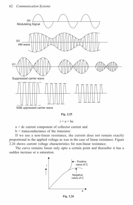
Modulating Signal
(a)
(b)
(c)
Suppressed carrier wave
AM wave
SSB uppressed carrier wave
Amplitude and Angle Modulation 63
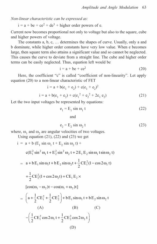
Non-linear characteristic can be expressed as:i = a + be + ce2 + de3 + higher order powers of e.
Current now becomes proportional not only to voltage but also to the square, cubeand higher powers of voltage.
The constants a, b, c, … determines the shapes of curve. Usually, only a andb dominate, while higher order constants have very low value. When e becomeslarge, then square term also attains a significant value and so cannot be neglected.This causes the curve to deviate from a straight line. The cube and higher orderterms can be easily neglected. Thus, equation left would be
i = a + be + ce2 (20)Here, the coefficient “c” is called “coefficient of non-linearity”. Let apply
equation (20) to a non-linear characteristic of FETi = a + b(e1 + e2) + c(e1 + e2)
2
i = a + b(e1 + e2) + c(e12 + e2
2 + 2e1 e2) (21)Let the two input voltages be represented by equations:
e1 = E1 sin ω1 t (22)
and
e2 = E2 sin ω2 t (23)where, ω1 and ω2 are angular velocities of two voltages.
Using equation (21), (22) and (23) we geti = a + b (E1 sin ω1 t + E2 sin ω2 t) +
2 2 2 21 1 2 2 1 2 1 2c(E sin t E sin t 2E E sin t sin t)ω + ω + ω ω
= 21 1 2 2 1 1
1a b E sin t b E sin t CE (1 cos 2 t)2
+ ω + ω + − ω
22 2 1 2
1 CE (1 cos 2 t) CE E2
+ + ω + ×
1 2 1 2[cos( )t cos( )t]ω − ω − ω + ω
=2 21 2 1 1 2 2
1 1a CE CE b E sin t b E sin t2 2
+ + + ω + ω
(A) (B) (C)
2 21 1 2 2
1 1CE cos 2 t CE cos 2 t2 2
− ω + ω
(D)

64 Communication Systems
1 2 1 2 1 2 1 2CE E cos( )t CE E cos( )t+ ω − ω − ω + ω (24)
(E) (F)
Equation (24) a very important relation and will be used at number of places.If we assume ω1 to be carrier angular frequency and ω2 as the modulating angularfrequency then term:
(A) represents dc current component,(B) represents carrier,(C) represents modulating signal,(D) represents the harmonics of carrier and modulating signal,(E) and (F) lower and upper sidebands respectively.The equation proves that when the two frequencies are passed simultaneously
through a non-linear resistance, amplitude modulation takes place. The output ofmodulation circuit can be tuned to the carrier frequency, having sufficient bandwidthso as to allow two sidebands and reject the other frequencies.
2.28 BALANCED MODULATOR (CARRIER SUPPRESSION)
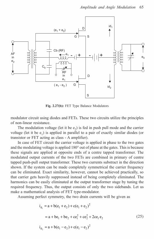
(DSB - SC):Balance modulator has a very important property of generating amplitude modulationand simultaneously suppressing the carrier. Figure 2.27 a and b shows the balance
Fig. 2.27(a): Diode Type Balance Modulator
Output
D1
D2
Cb
Cb
AFinput
Carrierinput
Amplitude and Angle Modulation 65
modulator circuit using diodes and FETs. These two circuits utilize the principlesof non-linear resistance.
The modulation voltage (let it be e2) is fed in push pull mode and the carriervoltage (let it be e1) is applied in parallel to a pair of exactly similar diodes (ortransistor or FET acting as class - A amplifier).
In case of FET circuit the carrier voltage is applied in phase to the two gatesand the modulating voltage is applied 180° out of phase at the gates. This is becausethese signals are applied at opposite ends of a centre tapped transformer. Themodulated output currents of the two FETs are combined in primary of centretapped push-pull output transformer. These two currents substract in the directionshown. If the system can be made completely symmetrical the carrier frequencycan be eliminated. Exact similarity, however, cannot be achieved practically, sothat carrier gets heavily suppressed instead of being completely eliminated. Theharmonics can be easily eliminated at the output transformer stage by tuning therequired frequency. Thus, the output consists of only the two sidebands. Let usmake a mathematical analysis of FET type-modulator.
Assuming perfect symmetry, the two drain currents will be given as
1d 1 2 1 2i a b(e e ) c(e e )2= + + + +
2 21 2 1 2 1 2a be be ce ce 2ce e= + + + + + (25)
2
2d 1 2 1 2i a b(e e ) c(e e )= + − + −
Fig. 2.27(b): FET Type Balance Modulators
D
G S
1id
(e + e )1 2
Cb
Cb (RF)e1 - + +-
D
S
id2( e - e )1 2
AFine2
e0
ine1
RF
G
Amplitude and Angle Modulation 67
2.29 UNWANTED SIDEBAND SUPPRESSION
Balance modulator suppresses the carrier. To obtain the SSB signal still anotherfrequency, i.e. the unwanted sideband has also to be removed. Three differentmethods are used. All three circuits have the capability to remove sidebands desiredby little change in circuit arrangement.
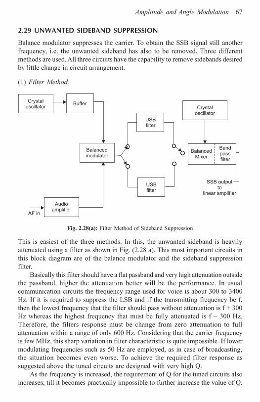
(1) Filter Method:
Fig. 2.28(a): Filter Method of Sideband Suppression
Crystaloscillator
Buffer
Balancedmodulator
USBfilter
Crystaloscillator
BalancedMixer
Bandpassfilter
USBfilter
Audioamplifier
AF in
SSB outputto
linear amplifier
This is easiest of the three methods. In this, the unwanted sideband is heavilyattenuated using a filter as shown in Fig. (2.28 a). This most important circuits inthis block diagram are of the balance modulator and the sideband suppressionfilter.
Basically this filter should have a flat passband and very high attenuation outsidethe passband, higher the attenuation better will be the performance. In usualcommunication circuits the frequency range used for voice is about 300 to 3400Hz. If it is required to suppress the LSB and if the transmitting frequency be f,then the lowest frequency that the filter should pass without attenuation is f + 300Hz whereas the highest frequency that must be fully attenuated is f – 300 Hz.Therefore, the filters response must be change from zero attenuation to fullattenuation within a range of only 600 Hz. Considering that the carrier frequencyis few MHz, this sharp variation in filter characteristic is quite impossible. If lowermodulating frequencies such as 50 Hz are employed, as in case of broadcasting,the situation becomes even worse. To achieve the required filter response assuggested above the tuned circuits are designed with very high Q.
As the frequency is increased, the requirement of Q for the tuned circuits alsoincreases, till it becomes practically impossible to further increase the value of Q.

68 Communication Systems
For upper frequency limit of the filters, it has been found that the multistageLC-filters cannot be used efficiently above 100 kHz, as above this frequency, theattenuation in the stop band becomes insufficient. Thus, crystal or mechanicalfilters are used for this purpose. Mechanical filters can be used upto 500 kHzusually, while crystal filters can go upto 20 MHz. Mechanical filters are the best asthey offer best all-round properties example:
Small size, very good attenuation characteristics, good bandpass and sufficientupper frequency limit. The crystal filter, works out to be cheaper, but is preferredonly at frequencies in excess of 1 MHz. The transmitting frequencies are stillhigher than operating frequencies of these filters. Thus, a balanced mixer is used.This mixer is similar to a balanced modulator, except that the sum frequency usedhere is much greater than the crystal oscillator frequency, than the upper sidebandis from the carrier, so that it can be selected with use of tuned circuits.
In balanced mixer, the SSB - signal from the filter is added to crystal oscillatorfrequency, so as to achieve the desired transmission frequency. This gives anadded advantage of changing the transmission frequency by just changing thecrystal oscillator frequency to desired value.
The output of mixer is fed to a chain of class-BRF amplifiers. These amplifiershave a linear transfer characteristics because the amplitude of SSB signal is variableand so cannot be fed to a class-C amplifier, which will lead to distortion.
(2) Phase-shift Method:This method uses two balanced modulators. The block diagram is shown in Fig.(2.28b).
Fig. 2.28(b)
Balancedmodulator
SSBlinear amplifier
chain
Adderor
subtractor
M2
Audioor
base-band signal
input
P2
90° - Phaseshifter
Audioamplifier
Carriersource
M1P1
Balancedmodulator
90° - Phaseshifter
Amplitude and Angle Modulation 69
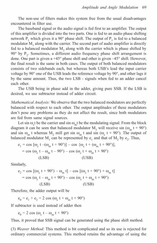
The non-use of filters makes this system free from the usual disadvantagesencountered in filter use.
The baseband signal or the audio signal is fed first to an amplifier. The outputof this amplifier is divided into the two parts. One is fed to an audio phase shiftingnetwork P1 which gives it a 90° phase shift. The output of P1 is fed to a balancedmodulator M1 along with the carrier. The second part of audio amplifier is directlyfed to a balanced modulator M2 along with the carrier which is phase shifted by90° by P2. Sometimes, a different audio frequency phase shift arrangement isdone. One part is given a +45° phase shift and other is given –45° shift. However,the final result is the same in both cases. The output of both balanced modulatorsconsists of two sidebands each, but whereas both USB’s lead the input carriervoltage by 90° one of the USB leads the reference voltage by 90°, and other lags itby the same amount. Thus, the two LSB - signals when fed to an adder canceleach other.
The USB being in phase add in the adder, giving pure SSB. If the LSB isdesired, we use subtractor instead of adder circuit.
Mathematical Analysis: We observe that the two balanced modulators are perfectlybalanced with respect to each other. The output amplitudes of these modulatorsdon’t pose any problems as they do not affect the result, since both modulatorsare fed from same signal sources.
Let sin ωct be the carrier and sin ωmt be the modulating signal. From the blockdiagram it can be seen that balanced modulator M1 will receive sin (ωm t + 90°)and sin ωm t whereas M2 mill get sin ωm t and sin (ωc t + 90°). The output ofbalanced modulator M1 can be represented by e1 and that of M2 by e2. Thus,
e1 = cos [ωc t –(ωm t + 90°)] – cos ωc t + (ωm t + 90°)],= cos (ωc t – ωm t – 90°) – cos (ωc t + ωm t + 90°)
(LSB) (USB)Similarly,
e2 = cos [(ωc t + 90°) – ωm t] – cos [(ωc t + 90°) + ωm t]= cos (ωc t – ωm t + 90°) – cos (ωc t + ωm t + 90°)
(LSB) (USB)Therefore, the adder output will be
e0 = e1 + e2 = 2 cos (ωc t + ωm t + 90°)
If subtractor is used instead of adder then
e0 = 2 cos (ωc t – ωm t + 90°)
Thus, it proved that SSB signal can be generated using the phase shift method.
(3) Weaver Method: This method is bit complicated and so its use is rejected forordinary commercial systems. This method retains the advantage of using the

Amplitude and Angle Modulation 71
Figure 2.29(a) shows a SSB pilot carrier radio transmitter, Fig. 2.29(b) showsthe frequency spectra of signals at various points within the system. The audiosignal (may be a telephone channel) in the frequency range 0–4 kHz (A) is fed tothe balanced modulator to create upper and lower sidebands around 100 kHz carrierposition (B)
Balancedmodulator
USB filter100–104
kHz
Balancedmodulator
Carrieroscillator100 kHz
Carrierattenuator
Band-passfilter
3 Mhzlinearpower
amplifier
3000to 3004 kHz
2900 kHz
(B) (C) (D)
(E)
AF input
Carrieroscillator2900 kHz
Fig. 2.29(a)
Fig. 2.29(b): Signal Spectra
USB
3000 kHz 3004 kHz
(E)
(D)
USBLSB
2900 kHz
Bandpass filterDifference
3000 kHz 3004 kHz
LSB USB
4 kHz 96 100 104 100 104 kHz
Pilot carrier
(A) (B) (C)
2796 kHz 2800 kHz SUM
An upper sideband filter passes the upper sideband between 100 and 104 kHz,to which the attenuated carrier is added to produce the signal (C). The reinsertedcarrier level is adjusted through the attenuator. This signal is now modulated on2900 kHz carrier by a second balanced modulator which acts as mixer to producean upper sideband of 3000 to 3004 kHz and lower sideband between 2800 and2796 kHz (Signal (D)). A bandpass filter passes the upper sideband and rejects thelower sideband to produce the signal (E) which is then amplified and transmitted.
72 Communication Systems
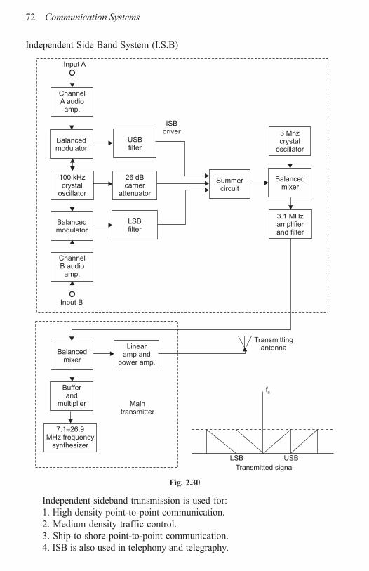
Independent sideband transmission is used for:1. High density point-to-point communication.2. Medium density traffic control.3. Ship to shore point-to-point communication.4. ISB is also used in telephony and telegraphy.
Input A
LSB USB
Transmitted signal
Maintransmitter
7.1–26.9MHz frequency
synthesizer
Bufferand
multiplier
Linearamp and
power amp.
Balancedmixer
Transmittingantenna
fc
Input B
ChannelB audio
amp.
LSBfilter
Balancedmodulator
3.1 MHzamplifierand filter
ISBdriver 3 Mhz
crystaloscillator
Balancedmixer
Summercircuit
100 kHzcrystal
oscillator
ChannelA audio
amp.
Balancedmodulator
USBfilter
26 dBcarrier
attenuator
Fig. 2.30
Independent Side Band System (I.S.B)
Amplitude and Angle Modulation 73
1. Inputs: Here two inputs are applied, say input A and input B. These inputs aredecided by international telecommunication union [I.T.U.]. According to I.T.U.applied inputs is of R3E modulation type. R3E modulation type means single side-band reduced carrier type. We know that receiver is tuned at different frequencies,for becoming tuning possible at different frequencies. For making demodulationeasy single sideband reduced carrier type modulation is used. These inputs aregiven independently to channel A and channel B audio amplifiers respectively. Theseinputs are transmitted simultaneously since inputs are independent one sideband isused for telephony and other sideband is used for telegraphy at receiving end.
2. Audio channel A and channel B amp: These amplifiers are used for amplifyingor raising voltage levels of SSB reduced carrier type input signals.
3. Balanced modulator: The 6 kHz channel A is fed to one balanced modulator;while another 6 kHz channel B is fed to another balanced modulator. 100 kHzcrystal oscillator output is given to both balanced modulator. Carrier is attenuatedby 45 dB or more by balanced modulator.
4. USB and LSB filter: USB filter will reject LSB and it will pass USB. On theother hand, LSB filter will reject USB and it will pass LSB.
5. Summer circuit: Outputs of USB filter and LSB filter and 26 dB attenuator aregiven to inputs of summer circuit. Output of summer circuit will be low frequencyISB, with pilot carrier present.
6. Crystal oscillator and Balanced mixer: 1 MHz crystal oscillator and balancedmixer will raise frequency level of signal from 100 kHz to 3.1 MHz. Balancedmixer will provide easier removal of unwanted frequencies with the help of outputfilter.
The signal is then given to main transmitter from ISB drive unit.
7. Frequency synthesizer, Buffer amplifier and multiplier and Balancedmixer: With the help of above 7.1 to 26.9 MHz frequency synthesizer, balancedmixer frequency of signal is again raised. This is done because this transmitter isused for HF band from 3 to 30 MHz.
8. Linear amplifier and power amplifier: Linear amplifier will raise voltage levelof signal and power amplifier will raise power level of signal. Typical power levelis generally 10 kW and 50 kW. This is fed to direction antenna for transmission.
Since width of channel is 6 kHz, it can carry two circuits of 3 kHz and hencefour conversation is possible simultaneously.
2.30 DEMODULATION OF AM
Diode-detector: A diode is the most widely used device for demodulation. Figure(2.31) shows a simple circuit using a diode for detection. It has a parallel RC
Amplitude and Angle Modulation 75
load resistance R of Fig. 2.31 is split here into two parts (R1 and R2) to obtain aseries dc path to ground for the diode. A low-pass filter R1 C1 is added to removeany RF ripple still represent. C2 is used to prevent any diode dc output reaching thevolume control resistance (R3). The R4C3 combination works as low-pass filterfor removing AF components, thus providing dc voltage whose amplitude isproportional to the carrier strength which can be very easily used for AGC.
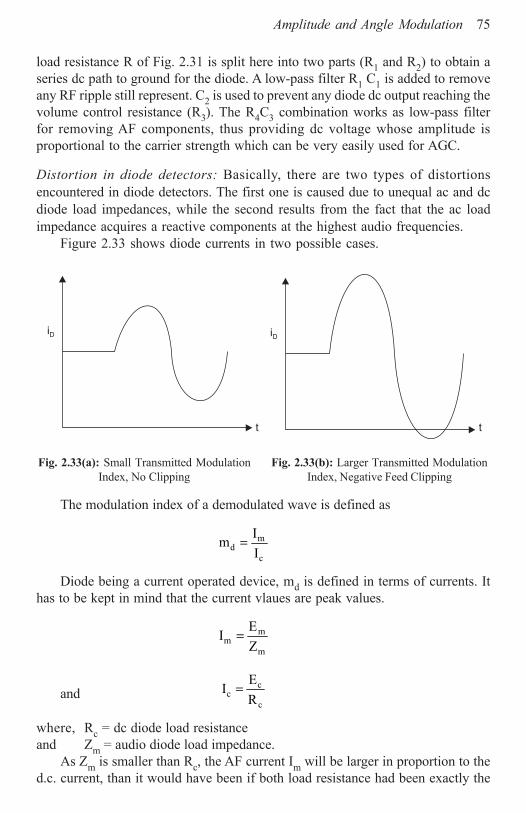
Distortion in diode detectors: Basically, there are two types of distortionsencountered in diode detectors. The first one is caused due to unequal ac and dcdiode load impedances, while the second results from the fact that the ac loadimpedance acquires a reactive components at the highest audio frequencies.
Figure 2.33 shows diode currents in two possible cases.
Fig. 2.33(b): Larger Transmitted ModulationIndex, Negative Feed Clipping
Fig. 2.33(a): Small Transmitted ModulationIndex, No Clipping
iD iD
t t
The modulation index of a demodulated wave is defined as
md
c
ImI
=
Diode being a current operated device, md is defined in terms of currents. Ithas to be kept in mind that the current vlaues are peak values.
mm
m
EIZ
=
andc
cc
EIR
=
where, Rc = dc diode load resistanceand Zm = audio diode load impedance.
As Zm is smaller than Rc, the AF current Im will be larger in proportion to thed.c. current, than it would have been if both load resistance had been exactly the

76 Communication Systems
same. In other words, the modulation index in the demodulated wave is higherthan the modulation index of the signal applied at the input of the diode detector.Thus, if we transmit a signal with 100% modulation there is every possibility ofover modulation to exist at the output of the detector.
The modulation index in the demodulated wave will be
Cm m md
c c c m
RI E / Zm mI E / R Z
= = =
Since the maximum allowable value of md is unity, the maximum value of mwill be
m mmax dmax
c c
Z Zm mR R
= =
(since mdmax = 1)In AM broadcasting system modulation index very unlikely crosses 70%. The
output of volume control resistance R3 is usually connected to the base of theaudio amplifier transistor. If the input impedance of this transistor is rather low, itwill load the detector reducing the diode audio load impedance. To overcome thisproblem, the first stage, of an audio amplifier should have a FET instead of abipolar transistor or a series resistance can be added in between the volume controlresistance R3 and the base of audio amplifier transistor.
But the latter solution reduces the volume fed to the audio amplifier, transistorthus reducing the output.
Diagonal clipping is the other form of trouble that may arise with diode detectors.At higher frequencies, the assumption that Zm is purely resistive may not workresulting in a reactive component of Zm due to C and C1. At high modulationdepths, current will be changing so quickly that the time constant of load may betoo slow to follow the change. This results in a exponential decay of currentinstead of following the waveform as shown in Fig. 2.34a.
Fig. 2.34(a): Diagonal Clipping
Clipping
Amplitude and Angle Modulation 77
Diagonal clipping does not normally occur, when modulation depth is below60%. Thus, it is possible to design a diode detector that is free from this type ofdistortion. The RC time constant for diode detector has to be properly designed.
2.31 DEMODULATION OF FM
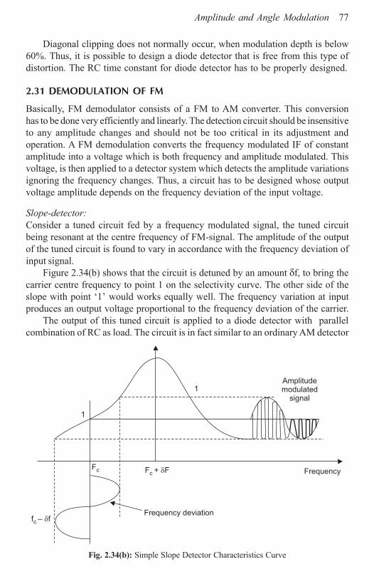
Basically, FM demodulator consists of a FM to AM converter. This conversionhas to be done very efficiently and linearly. The detection circuit should be insensitiveto any amplitude changes and should not be too critical in its adjustment andoperation. A FM demodulation converts the frequency modulated IF of constantamplitude into a voltage which is both frequency and amplitude modulated. Thisvoltage, is then applied to a detector system which detects the amplitude variationsignoring the frequency changes. Thus, a circuit has to be designed whose outputvoltage amplitude depends on the frequency deviation of the input voltage.
Slope-detector:Consider a tuned circuit fed by a frequency modulated signal, the tuned circuitbeing resonant at the centre frequency of FM-signal. The amplitude of the outputof the tuned circuit is found to vary in accordance with the frequency deviation ofinput signal.
Figure 2.34(b) shows that the circuit is detuned by an amount δf, to bring thecarrier centre frequency to point 1 on the selectivity curve. The other side of theslope with point ‘1’ would works equally well. The frequency variation at inputproduces an output voltage proportional to the frequency deviation of the carrier.
The output of this tuned circuit is applied to a diode detector with parallelcombination of RC as load. The circuit is in fact similar to an ordinary AM detector
Fig. 2.34(b): Simple Slope Detector Characteristics Curve
Fc F + Fc
Frequency deviation
Frequency
Amplitudemodulated
signal
1
1
f – fc
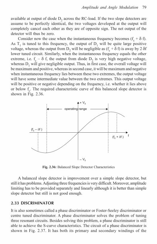
Amplitude and Angle Modulation 79
available at output of diode D2 across the RC-load. If the two slope detectors areassume to be perfectly identical, the two voltages developed at the output willcompletely cancel each other as they are of opposite sign. The net output of thedetector will thus be zero.
Consider now the case when the instantaneous frequency becomes (fc + δ f).As T1 is tuned to this frequency, the output of D1 will be quite large positivevoltage, whereas the output from D2 will be negligible as (fc + δ f) is away by 2 δflower tuned circuit. Similarly, when the instantaneous frequency equals the otherextreme, i.e. fc – δ f, the output from diode D2 is very high negative voltage,whereas D1 will give negligible output. Thus, in first case, the overall voltage willbe maximum and positive, whereas in second case, it will be maximum and negativewhen instantaneous frequency lies between these two extremes, the output voltagewill have some intermediate value between the two extremes. This output voltagewill be positive or negative depending on the frequency, i.e. whether it lies aboveor below fc. The required characteristic curve of this balanced slope detector isshown in Fig. 2.36.
V0+
operating range
(f f )c –
(f + )c f f
V0–
Fig. 2.36: Balanced Slope Detector Characteristics
A balanced slope detector is improvement over a simple slope detector, butstill it has problems. Adjusting three frequencies is very difficult. Moreover, amplitudelimiting has to be provided separately and linearly although it is better than simpleslope detector but still is not good enough.
2.33 DISCRIMINATOR
It is also sometimes called a phase discriminator or Foster-Seeley discriminator orcentre tuned discriminator. A phase discriminator solves the problem of tuningthree resonant circuits. Besides solving this problem, a phase discriminator is stillable to achieve the S-curve characteristics. The circuit of a phase discriminator isshown in Fig. 2.37. It has both its primary and secondary windings of the
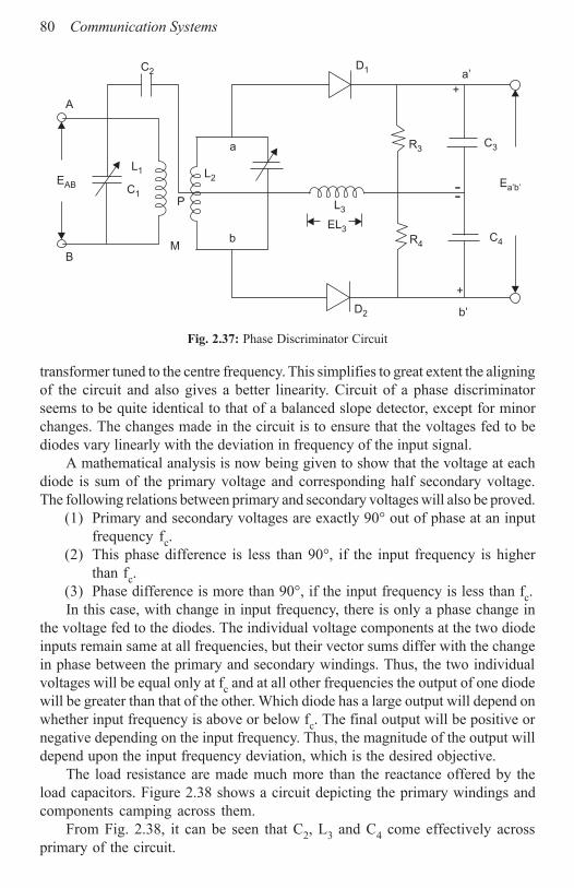
80 Communication Systems
transformer tuned to the centre frequency. This simplifies to great extent the aligningof the circuit and also gives a better linearity. Circuit of a phase discriminatorseems to be quite identical to that of a balanced slope detector, except for minorchanges. The changes made in the circuit is to ensure that the voltages fed to bediodes vary linearly with the deviation in frequency of the input signal.
A mathematical analysis is now being given to show that the voltage at eachdiode is sum of the primary voltage and corresponding half secondary voltage.The following relations between primary and secondary voltages will also be proved.
(1) Primary and secondary voltages are exactly 90° out of phase at an inputfrequency fc.
(2) This phase difference is less than 90°, if the input frequency is higherthan fc.
(3) Phase difference is more than 90°, if the input frequency is less than fc.In this case, with change in input frequency, there is only a phase change in
the voltage fed to the diodes. The individual voltage components at the two diodeinputs remain same at all frequencies, but their vector sums differ with the changein phase between the primary and secondary windings. Thus, the two individualvoltages will be equal only at fc and at all other frequencies the output of one diodewill be greater than that of the other. Which diode has a large output will depend onwhether input frequency is above or below fc. The final output will be positive ornegative depending on the input frequency. Thus, the magnitude of the output willdepend upon the input frequency deviation, which is the desired objective.
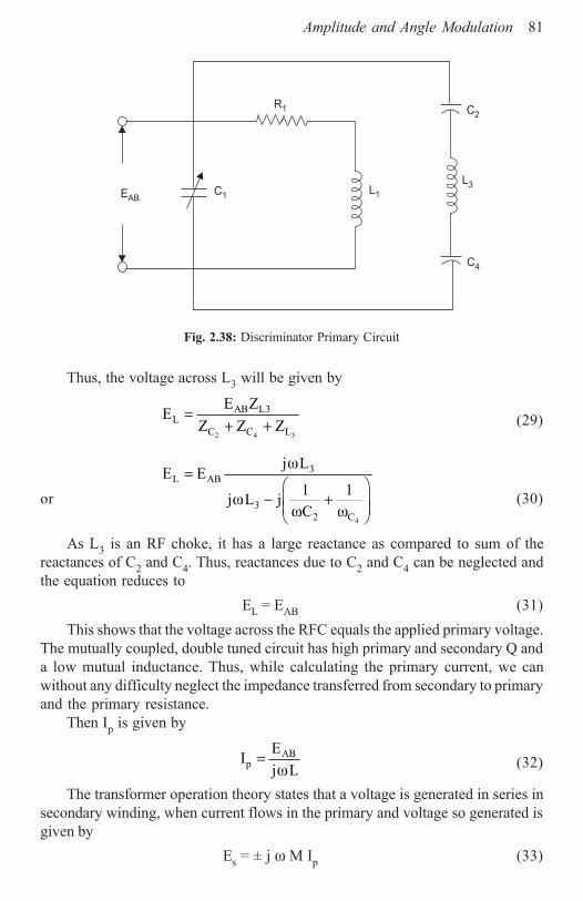
The load resistance are made much more than the reactance offered by theload capacitors. Figure 2.38 shows a circuit depicting the primary windings andcomponents camping across them.
From Fig. 2.38, it can be seen that C2, L3 and C4 come effectively acrossprimary of the circuit.
Fig. 2.37: Phase Discriminator Circuit
a
b
L2
D2 b’
+
R4C4
EL3
L3
Ea’b’
C3R3
--
+
a’D1
P
M
C1
L1
C2
B
EAB
A
Amplitude and Angle Modulation 81
Thus, the voltage across L3 will be given by
2 4 3
AB L3L
C C L
E ZEZ Z Z
=+ + (29)
or4
3L AB
32 C
j LE E
1 1j L jC
ω=
ω − + ω ω
(30)
As L3 is an RF choke, it has a large reactance as compared to sum of thereactances of C2 and C4. Thus, reactances due to C2 and C4 can be neglected andthe equation reduces to
EL = EAB (31)This shows that the voltage across the RFC equals the applied primary voltage.
The mutually coupled, double tuned circuit has high primary and secondary Q anda low mutual inductance. Thus, while calculating the primary current, we canwithout any difficulty neglect the impedance transferred from secondary to primaryand the primary resistance.
Then Ip is given by
ABp
EIj L
=ω (32)
The transformer operation theory states that a voltage is generated in series insecondary winding, when current flows in the primary and voltage so generated isgiven by
Es = ± j ω M Ip (33)
Fig. 2.38: Discriminator Primary Circuit
L1
R1
C1EAB
C2
L3
C4
Amplitude and Angle Modulation 83
ak ap L ab AB1E E E E E2
= + = + (36)
bk bp L ap LE E E E E= + = − +
bk ab AB1E E E2
= − + (37)
It can be seen that the voltage applied to each diode is the sum of the primaryvoltage and corresponding half secondary voltage. The dc voltage conditions cannotbe evaluated as d.c. diode drop is not known. However, it is known that each willbe proportional to the peak value of the RF voltage applied to the respective diode.Therefore,
a b a k b kE E E′ ′ ′ ′= −
or a b ak bkE E E′ ′ α − (38)
At input frequency fin equal to fc, X2 becomes zero, so that eqn. (35) reducesto
5AB Cab
1 2
E XjMEL R
=
5AB Cab
1 2
E XME 90L R
= ∠ ° (39)
Equation (39) proves that the secondary voltage Eab leads the applied primaryvoltage EAB by 90°C.
Therefore, –Eab will lag EAB by 90°. It now becomes possible to add the diodeinput voltages vectorially as shown in Fig. 2.40.
At this stage, i.e. when fin = fc the two voltages Eak and Ebk will be equal sothat the discriminator output will be zero. Thus, at the carrier frequency or inother words an unmodulated carrier frequency produces a zero voltage at thediscriminator output. But it will be seen that at any other frequency there will be anoutput.
If fin is greater than fc then equation (35), XL2 becomes greater than
5CX sothat X2 becomes positive. Therefore, equation (35) takes the form
5AB Cab
1 2 2
E XjMEL R jX
= ×+
5AB Cab
1 2
M E X 90EL | Z | 0
∠ °=∠ ° (40)

84 Communication Systems
Equation (40) shows that Eab leads EAB by less than 90° and therefore –Eabwill lag EAB by more than 90°. Figure 2.41 shows this case. Here, Eak is greaterthan Ebk showing that discriminator output will be positive when fin is greater thanfc. If input frequency is less than fc, X2 becomes negative and the angle of impedanceZ2 will also become negative. This causes Eab to lead EAB by more than 90°. Thefinal output of discriminator is found to be negative in this case.
A phase discriminator has only tuned circuits to be tuned to a single frequency,so that its alignment is much easier as compared to balanced slope detector. Thelinearity is better because the circuit uses less of frequency response and more ofprimary secondary phase relations which are more linear. A phase discriminator,however, provides no amplitude limiting which of course is a disadvantage with it.
Fig. 2.42
Fig. 2.41
Fig. 2.40
EAB
EAB
Eak
EAB
Ebk
F Fin = c
1
2–
1
2
EAB
EAB
F > Fin c
EAB
Ebk
Eak
1
2–
1
2
EAB
EAB
Eak
EAB
Ebk
F < Fin c
1
2–
1
2
Amplitude and Angle Modulation 85
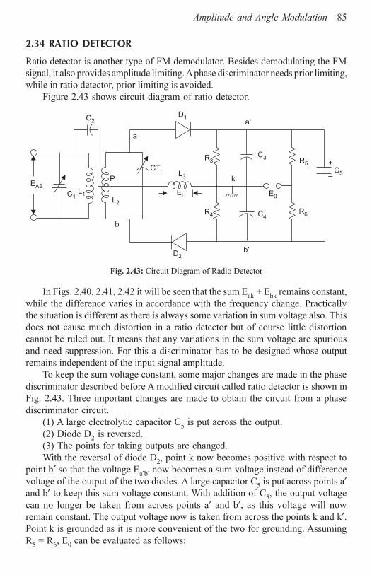
2.34 RATIO DETECTOR
Ratio detector is another type of FM demodulator. Besides demodulating the FMsignal, it also provides amplitude limiting. A phase discriminator needs prior limiting,while in ratio detector, prior limiting is avoided.
Figure 2.43 shows circuit diagram of ratio detector.
C5
C3
C4
R5
R6
k
R3
R4
L3
EL
CTr
a
D1
D2
P
L2
b
L1C1
EAB
C2 a
b’
E0
+
–
Fig. 2.43: Circuit Diagram of Radio Detector
In Figs. 2.40, 2.41, 2.42 it will be seen that the sum Eak + Ebk remains constant,while the difference varies in accordance with the frequency change. Practicallythe situation is different as there is always some variation in sum voltage also. Thisdoes not cause much distortion in a ratio detector but of course little distortioncannot be ruled out. It means that any variations in the sum voltage are spuriousand need suppression. For this a discriminator has to be designed whose outputremains independent of the input signal amplitude.
To keep the sum voltage constant, some major changes are made in the phasediscriminator described before A modified circuit called ratio detector is shown inFig. 2.43. Three important changes are made to obtain the circuit from a phasediscriminator circuit.
(1) A large electrolytic capacitor C5 is put across the output.(2) Diode D2 is reversed.(3) The points for taking outputs are changed.With the reversal of diode D2, point k now becomes positive with respect to
point b′ so that the voltage Ea′b′ now becomes a sum voltage instead of differencevoltage of the output of the two diodes. A large capacitor C5 is put across points a′and b′ to keep this sum voltage constant. With addition of C5, the output voltagecan no longer be taken from across points a′ and b′, as this voltage will nowremain constant. The output voltage now is taken from across the points k and k′.Point k is grounded as it is more convenient of the two for grounding. AssumingR5 = R6, E0 can be evaluated as follows:
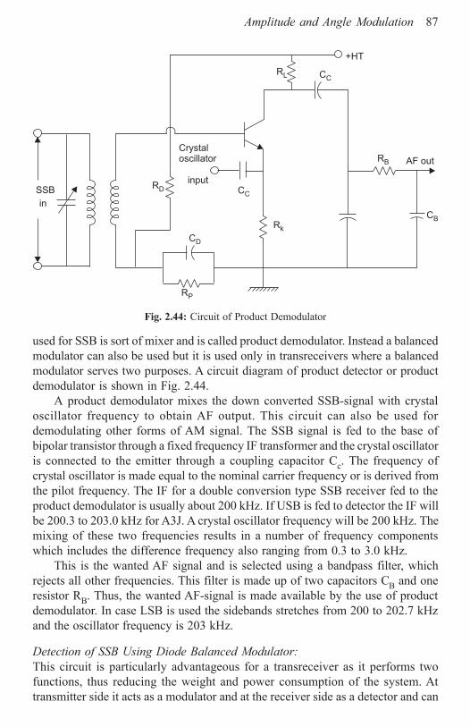
Amplitude and Angle Modulation 87
used for SSB is sort of mixer and is called product demodulator. Instead a balancedmodulator can also be used but it is used only in transreceivers where a balancedmodulator serves two purposes. A circuit diagram of product detector or productdemodulator is shown in Fig. 2.44.
A product demodulator mixes the down converted SSB-signal with crystaloscillator frequency to obtain AF output. This circuit can also be used fordemodulating other forms of AM signal. The SSB signal is fed to the base ofbipolar transistor through a fixed frequency IF transformer and the crystal oscillatoris connected to the emitter through a coupling capacitor Cc. The frequency ofcrystal oscillator is made equal to the nominal carrier frequency or is derived fromthe pilot frequency. The IF for a double conversion type SSB receiver fed to theproduct demodulator is usually about 200 kHz. If USB is fed to detector the IF willbe 200.3 to 203.0 kHz for A3J. A crystal oscillator frequency will be 200 kHz. Themixing of these two frequencies results in a number of frequency componentswhich includes the difference frequency also ranging from 0.3 to 3.0 kHz.
This is the wanted AF signal and is selected using a bandpass filter, whichrejects all other frequencies. This filter is made up of two capacitors CB and oneresistor RB. Thus, the wanted AF-signal is made available by the use of productdemodulator. In case LSB is used the sidebands stretches from 200 to 202.7 kHzand the oscillator frequency is 203 kHz.
Detection of SSB Using Diode Balanced Modulator:This circuit is particularly advantageous for a transreceiver as it performs twofunctions, thus reducing the weight and power consumption of the system. Attransmitter side it acts as a modulator and at the receiver side as a detector and can
Fig. 2.44: Circuit of Product Demodulator
CB
AF outRB
CD
CC
Rk
CCRL
RDinput
Crystaloscillator
RP
+HT
SSB
in

88 Communication Systems
be switched on to either side when required. A diode balanced modulator is shownin Fig. 2.45.
The local oscillator frequency is either 200 or 203 kHz depending upon thesideband to be demodulated. The output of local-crystal oscillator is fed to terminalA A′. In case of modulator the carrier suppressed signal is taken out from terminalsCC′, but while using it as a demodulator, we feed in the SSB-signal at these points.This circuit now behaves as a non-linear resistance resulting in sum and differencefrequencies at the AF transformer primary. The transformer stops the RF frequenciesand allows only AF signals to terminals BB′ thus avoiding the use of a separatelow-pass filter. The circuit easily drives out the modulating information on theSSB-signal and works quite similarly to product detector.
2.36 VSB (VESTIGAL SIDEBAND) TRANSMISSION
SSB signals are relatively difficult to generate. The bandwidth of composite videosignal is limited to 4 MHz, using maximum modulation frequency of 4 MHz,amplitude modulation of carrier results in two sidebands each of 4 MHZ width sothat the total bandwidth requirement for channel amounts to 9 MHz. The bandwidthis large. Bandwidth required may be reduced by utilizing the fact that the entiresignal information is contained in each of the two sidebands of the modulatedcarrier. Thus, we may use only one sideband and the carrier and suppress theother sideband, thereby reducing the bandwidth requirement to half, i.e. MHz. ButTV signals extend down to zero frequency and removal of one sideband from therest becomes practical impossibility. Hence, in practice, only a part of one sidebandis suppressed.
Fig. 2.45
B
B
A
A
D1
AFout
Crystaloscillatorinput
D2
C
C
SSBin

Amplitude and Angle Modulation 89
More the information that must be sent in given time, the larger is the bandwidthrequired. The simplify video demodulation in the receiver, the carrier is, in practice,sent undiminished. Because the phase response of filters, near the edges of the flatpass band, would have a harmful effect on the received video signals in TV receiver,a portion of unwanted (lower) sidebands must also be transmitted. The result isVSB-transmission or C3F as shown in Figs. 2.46 and 2.47.
By sending the first 1.25 MHz of the lower sideband (the first 0.75 MHz of itundiminished) if it possible to make sure that the lowest frequencies in the wantedupper sideband are not distorted in phase by the VSB filter. Because only first 1.25
Fig. 2.46: Spectrum of Transmitted Signal
1.0
Picturecarrier
0.5
Relativeamplitude
Videolowersideband
Videouppersideband
00.5 1.25 Relative Channel
freqency5.25 5.75 6
4 MHz
4.5 MHz
0.75MHz
SoundcarrierSound
spectrum(width = 50 kHz)
1
0.5
Relativeresponse
0 1.25 2.5 Video frequency 5.2 5.75 6
4 MHz
Picturecarrierfrequency
Sound carrierfrequency
Fig. 2.47: Corresponding Receiver Amplifier Frequency Response
90 Communication Systems
MHz of the lower sideband is transmitted, 3 MHz of spectrum is saved for everyTV-channel. Since the total bandwidth requirement of a television channel is now6 MHz instead of 9 MHz, clearly a great saving has been made, and more channelsconsequently can be accommodated.
All these signals occupy frequencies near the video transmissions simplybecause sound is required with the pictures and it would not be very practical tohave a completely separate receiver for the sound, operating at some frequencyremote from the video transmitted frequencies.
Attenuation is purposely provided for the video frequencies from 0 to 1.25MHz. The reason is extra power is transmitted at these frequencies. Accordingly,these frequencies would be unduly emphasized in the video output of the receiverif they were not attenuated appropriately.
NumericalsExample 2.8: The voltage of certain amplitude modulated wave is expressed as:
v = 10 (1 + 3 cos (2π × 1000 × t)) × [cos 2π × 106 × t]
Calculate (a) ma = ? (b) fc and (c) fm.
Solution: v = 10 [1 + 3 cos (2π × 1000 × t))] ×
[cos 2π × fc × t] (*)
Standard form V = Ec[1 + ma cos (2π × fm × t))]
× [cos 2π × fc × t] (*)(*)
Comparing (*) and (**) we have
(a) ma = 3
(b) fm = 1000 Hz = 1 kHz and
(c) fc = 106 Hz = 1 MHz
Example 2.9: A bandwidth of 20 MHz is to be considered for the transmission ofAM signals. If the highest audio frequencies used to modulate the carriers are notto exceed 3 kHz, how many stations could broadcast within this bandsimultaneously without interfering with one another?
Solution: Given Total bandwidth = 20 MHzfa max = 3 kHz
Find : Number of AM stations.The maximum bandwidth of each AM station is determined by the maximum
frequency of the modulating signal.Station B.W. = 2 fa max
= 2 × 3 × 103 = 6 × 103 = 6 kHz
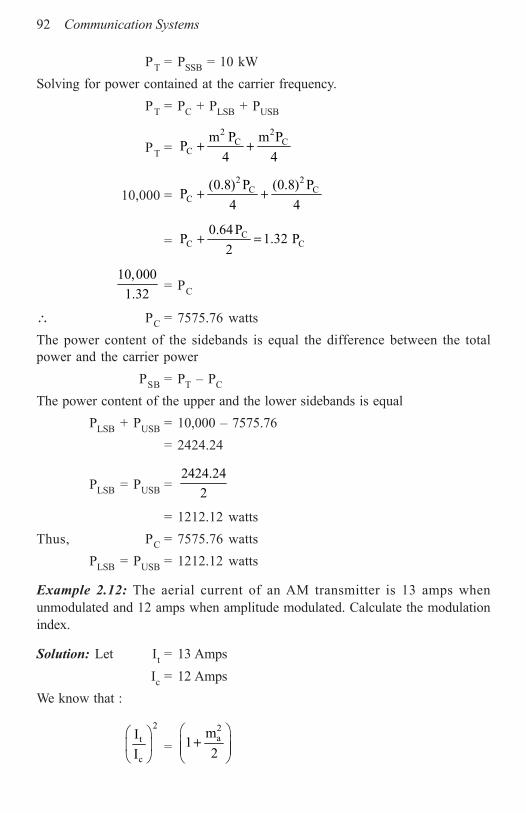
92 Communication Systems
PT = PSSB = 10 kWSolving for power contained at the carrier frequency.
PT = PC + PLSB + PUSB
PT =2 2
C CC
m P m PP4 4
+ +
10,000 =2 2
C CC
(0.8) P (0.8) PP4 4
+ +
= CC C
0.64PP 1.32 P2
+ =
10,0001.32 = PC
∴ PC = 7575.76 wattsThe power content of the sidebands is equal the difference between the totalpower and the carrier power
PSB = PT – PC
The power content of the upper and the lower sidebands is equalPLSB + PUSB = 10,000 – 7575.76
= 2424.24
PLSB = PUSB =2424.24
2
= 1212.12 wattsThus, PC = 7575.76 watts
PLSB = PUSB = 1212.12 watts
Example 2.12: The aerial current of an AM transmitter is 13 amps whenunmodulated and 12 amps when amplitude modulated. Calculate the modulationindex.
Solution: Let It = 13 AmpsIc = 12 Amps
We know that :
2t
c
II
=2am1
2
+

Amplitude and Angle Modulation 93
2t
c
11
I
−
=2ma
2
∴ ma2 =
2t
c
I2 1I
−
∴ ma =
2t
c
I2 1
I
−
∴ ma =2132 1
12
−
∴ ma = 0.5
Example 2.13: A 75 MHz carrier having an amplitude of 50 V is modulate by a 3kHz audio signal having an amplitude of 20 V.Calculate: (a) Modulation index (m)
(b) What frequencies would show up in a spectrum analysis ofmodulated wave.
(c) Write trigonometric equations for carrier and the modulatingwaves.
Solution: (a) From the defining equation of modulation factor.
m =m
c
EE
∴ m =20 0.450
=
(b) The frequency content of an AM signal consists of the carrier frequency andthe sideband frequencies which result from adding the audio frequency to thecarrier and from subtracting the audio frequency from the carrier frequency.
fc = 75 kHz
fc + fa = 75 MHz + 3 kHz
= 75000 kHz + 3 kHz = 75003 kHz
fc – fa = 75,000 kHz – 3 kHz = 74997 kHz
94 Communication Systems
Thus, the frequency content of the AM wave is
75.000 MHz75.003 MHz74.997 MHz
(c) Va = Em sin 2π fat
= 20 sin 2π (3000) t
Va = 20 sin 6000 π t
and Vc = Ec sin 2π fct
= 50 sin 2π (75 × 106) t
Vc = 50 sin 150 × 106 π t
Example 2.14: The trapezoidal pattern shown in figure results when examining anAM wave. Determine the modulation index. What can be said about the distortionof the AM wave.
Solution: Trapezoidal pattern shown in figure.
L = 5 cm1 L = cm2 2
m =1 2
1 2
L L 5 2 3L L 5 2 7
− −= =+ +
% m =3 100 42.97× =
m = 42.9 %Regarding distortion: Since the sides of the trapezoid pattern show very little,
if any curvature, it can be said that there is very little, if any, distortion of themodulated wave.
Example 2.15: An AM broadcast station operates at its maximum allowed totaloutput of 50 kW and with 95% modulation.

96 Communication Systems
Example 2.17: Determine the power in the sidebands as a percentage of the totalpower of modulated signal in the case of a carrier amplitude modulated by twosinusoidal signals of different frequencies, with individual modulation depths of0.3 and 0.4.
Solution: Assume carrier power to be PcThe total sideband power would be
2 2Cm x (t) P
where 1 2 1m x (t) 0.3cos t 0.4cos t, here and= ω + ω ωω2 are two modulating frequencies
So that 2 2 21 2m x (t) (0.3 cos t 0.4cos t) ,= ω + ω averaged over a suitable
period
∴ 2 2m x (t) =2 21 [(0.3) (0.4) ] 0.1250
2 + =
Also 2 Psb = 0.1250 Pc
and Pt = Pc + 2 Psb
∴ Pt = Pc + 0.1250 Pc
Pt = 1.1250 Pc
Total sideband power =c
c
0.1250 P or 11.1%1.125 P
Example 2.18: An AM signal is represented byV(t) = [10 + 4 sin 1000 πt] + [cos (2π × 106)t] V
Amplitude
0.025 V
0.005 V
0.1 V
0.005 V
0.025 V
Frequency(kHz)
0 1589 1589.6 1590 1590.4 1591
Amplitude and Angle Modulation 97
where t is expressed in second.Determine frequency of modulating signal, the frequency of carrier, the index
of modulation and fractional power in each sidebond.
Solution: Referring to the standard relation for an AM signal.We have: Angular frequency of the modulating signal = 1000 π rad/sec.
corresponding to 500 Hz. Angular frequency of carrier = 2π × 106 rad/sec.corresponding to 106 Hz or 1 MHz
Also modulation index m =4
10 = 0.4
Power in carrier = PC = (10)2 = 100 units
Sideband amplitude =12 × 4 = 2 V
Sideband power = 22 = 4 unitsTotal sideband power = 2 × 4 = 8 units
Total signal power = (100 + 8) 108 unitsHence, fractional power in each
Sideband =4
108 = 0.037
Example 2.19: A class c amplifier, with an output of 5 kW, operates an efficiencyof 80% from a 500 V anode supply.If the amplifier is to be anode modulated to a depth of 70%, find
(i) the required power output of the modulating signal amplified and(ii) The load impedance presented to this amplifier.
Solution: Pc = 5 kWη1 = 80% = 0.8
Pd.c. =5
0.8
= 6.25 kW = 6250 watts
Vd.c. = 5000 V,
Id.c. =62505000
= 1.25 A
Rd.c. = 5000 40001.25
= Ω
m = 0.7
PSB =12
m2 Pc
98 Communication Systems
=12
(0.7)2 × 5000 = 1225 W
Pm out =1225 1225 1531 watts
0.80 = = η
Ra.c. = Rd.c. = 4000 Ω
Example 2.20: A transistor class C amplifier has maximum permissible collectordissipation of 20 watts and collector efficiency of 75%. It is to be collectormodulated to a depth of 90%. Calculate (i) Maximum carrier power and (ii) sidebandpower that are generated.
Solution: Given data(i) Maximum permissible collector dissipation with no modulation is given by
1maxCP = 20 watts
Collector efficiency = ηC = 0.75Power from collector supply source is given by
PCC =C C
C
P P0.75
=η
Maximum permissible collector dissipation with no modulation is given by
1maxCP = (Pcc – Pc max)
=cmax
cmaxP
P0.75
−
∴ 1maxCP = maxC1 1 P
0.75 1 −
∴ 20 watts = maxC0.25P0.75
∴maxCP = 20 × 3 = 60 watts
Maximum carrier power = 60 watts
(ii)maxSBP =
max max max
2
LSB USB Cm 1P P P2 2
= = × ×
∴maxSBP =
2(0.9) 1602 2
× ×

Amplitude and Angle Modulation 99
=160 0.452
× ×
∴maxSBP = 2.4 watts = 1.2 watts
Example 2.21: If a 6 MHz band were being considered for use with same standardsthat apply to the 88–108 MHz band, how many FM stations could be accommodated?
Solution: B.W. = 6 MHzFind : Number of stationsEach station requires a total bandwidth of 400 kHz; 150 kHz for the signal and a 25kHz guard band above and below with only alternative channels used
Number of stations =6
36 10 15
400 10× =×
Number of stations = 15
Example 2.22: A carrier of 90 MHz with 5 V peak amplitude. A modulating signalof 5 V peak amplitude and frequency of 5 kHz. The frequency deviation constantis 1 kHz/volt. Determine the bandwidth of the frequency modulated signal.
Solution: Given dataδ = 1 kHz/V,
fm = 5 kHz
We know mf =15 = 0.2
We have, (BW)FM = 2(mf + 1) fm = 2(0.2 + 1) × 5 kHz(BW)FM = 12 kHz
Example 2.23: A 1 MHz carrier of 10 V amplitude, when frequency modulated bya 400 Hz, 1 volt modulating signal, undergoes 1 kHz deviation. If the modulatingsignal frequency changed to 1 kHz with 2 V amplitude, determine the bandwidthof the signal.
Solution: Here fc = 1 MHzAc = 1 Vfm = 400 Hz
Am = 1 Vfm = 1 kHz
Amplitude and Angle Modulation 101
Frequency deviation = (0.25 × 1000) = 250 HzRequired deviation = 75 kHz = 75,000 Hz
Required frequency multiplication =75,000 300
250=
Carrier frequency = 100 MHzInitial frequency = 500 kHz
Frequency multiplication =6
3100 10500 10
××
= 200Since frequency multiplication are different to meet the two requirements, frequencyconversion has to be resorted to the multiplication factors can be:
300 = 2 × 2 × 3 × 5 × 5Multiplying by 2, 3, and 5 kHz and then superheterodyning 500 kHz × 2 × 3 × 5
Frequency conversion = 2 × 50 = 100 MHzHere the frequency convertor output frequency has to be
100 52
×
= 15000 kH
= 15 MHzSo the required frequency convertor heterodyning frequency would be
(15 ± 10) MHz = 25 MHz or 5 MHz.
Example 2.26: An FM signal is produced through the generation of a narrow-band PM signal. The NBM signal is obtained as a combination of a DSB – SCsignal and a 90° phase shifted carrier. The depth of modulation in this combinedsignal, corresponds to m = 0.2. The modulating signal frequency is 100 Hz. It isdesired to generate an FM signal with 25 kHz deviation. Suggest appropriatefrequency multiplier chain.
Solution: Depth of amplitude modulation= m = 0.2 it is also m of NBPM also,
Maximum phase modulation = 0.2 radMaximum frequency deviation = (0.2 × 100) Hz
Required deviation = 25 kHz
Required frequency multiplication factor =25000
20
= 1250
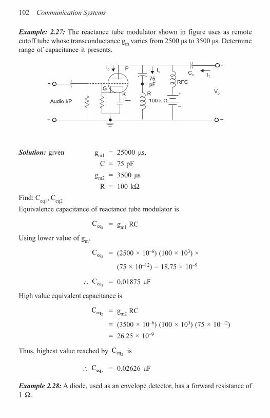
102 Communication Systems
Example: 2.27: The reactance tube modulator shown in figure uses as remotecutoff tube whose transconductance gm varies from 2500 µs to 3500 µs. Determinerange of capacitance it presents.
G
ip P I1
75pF
R
100 k
K
RFC
Cc IT
Vp
Audio I/P
+
–
+
–
–
+
Solution: given gm1 = 25000 µs,C = 75 pF
gm2 = 3500 µsR = 100 kΩ
Find: Ceq1, Ceq2
Equivalence capacitance of reactance tube modulator is
1eqC = gm1 RC
Using lower value of gm,
1eqC = (2500 × 10–6) (100 × 103) ×
(75 × 10–12) = 18.75 × 10⁻⁹
∴1eqC = 0.01875 µF
High value equivalent capacitance is
2eqC = gm2 RC
= (3500 × 10–6) (100 × 103) (75 × 10–12)= 26.25 × 10⁻⁹
Thus, highest value reached by 2eqC is
∴2eqC = 0.02626 µF
Example 2.28: A diode, used as an envelope detector, has a forward resistance of1 Ω.
Amplitude and Angle Modulation 103
If detector load is a parallel combination of a 1000 Ω resistor and a 1000 pFcapacitor find the maximum permissible depth of modulation so as to avoid diagonalclipping, with modulating signal frequency values of (i) 100 Hz (ii) 1 kHz and (iii)10 kHz.Solution: (i) fm = 100 Hz
R = 1000 ΩC = 10000 pF
Hence 2π fm RC = 2 × 3.14 × 100 × 1000 × 1000 × 10–12
= 6.28 × 10⁻³
Hence, mmax = [1 + (6.28 × 10⁻³)2]–1/2
= 0.994(ii) fm = 1 kHz
Here 2π fm RC = 6.28 × 10⁻²
So that mmax = [1 + (6.28 × 10⁻²)2]–2
= 0.997(iii) fm = 10 kHz
Hence, 2π fm RC = 0.628So that mmax = [1 + (0.628)2]–1/2
= 0.847
Example 2.29: A non-linear device, with an output-input relation of i = [10 + 2Vi+ 0.2 Vi
2] mA, is supplied with a carrier of 1 V amplitude and sinusodal signal of0.5 V amplitude in series.Estimate the depth of modulation of the AM signal at the output, considering onlythe frequency components of the AM signal at the output.
Solution: The input signal is given byVi (t) = cos ωct + 0.5 cos ωmt
with the usual notations.The output current is given by
i = 10 + (cosωct + 0.5 cos ωmt) +0.2 (cos ωct + 0.5 cos ωmt)2 mA
The carrier frequency term is 2 cos ωct, while the (fc ± fm) frequency term is
0.2 × 2 × 0.5 cos ωct cos ωmt or 0.2 cos ωmt.The remaining terms would not contribute to the AM signal at the carrier
frequency fc. So, the AM signal would be 2 cos ωct + 0.2 cos ωct cos ωmtcorresponding to m = 0.1 or 10%.
Amplitude and Angle Modulation 105
∴S.S.B.
SN
= 2
D.S.B.
2 S1Nm
+
∴S.S.B.
SN
=
21 40 dB(0.5)2
+ ×
∴S.S.B.
SN
= 360 dB
Example 2.32: In a certain SSB generator of the phase-shift type, the carrier inputto one of the modulators fall to 98% of correct amplitude.
Determine its effect on the SSB output.
Solution: Assume reduced carrier input is to be applied to the modulator B.
So, output of modulator A = cos ωct · sin ωmt
Output of modulator B = 0.98 sin ωct · sin ωmt
Difference between outputs = cos ωct · cos ωmt – 0.98
sin ωct · sin ωmt
= (0.99 + 0.01) cos ωct · cos ωmt –
(0.99 – 0.01) sin ωct · sin ωmt
= 0.99 cos (ωc + ωm)t + 0.01
cos (ωc + ωm)t
Example 2.33: In a series plate modulated amplifier, plate supply voltage is 300volts and the DC plate current under unmodulated condition is 20 amp. The sinusoidalmodulating voltage which appears in the plate circuit of modulated amplifier hasamplitude of 150 volts. The unmodulated output carrier power is 4.5 kW. Calculate(i) modulation index (ii) carrier power under modulated condition (iii) plate circuitefficiency and (iv) plate dissipation under unmodulated and modulated conditions.
Solution: (i) Modulation index
ma =mm
bb
V 150 0.5V 300
= =
(ii) Carrier power under modulated condition is given by
P =2
CmP 12
+
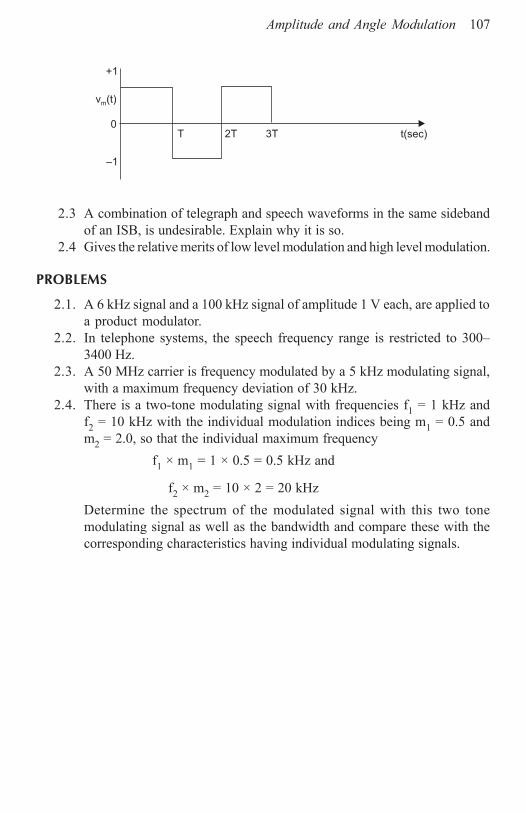
Amplitude and Angle Modulation 107
2.3 A combination of telegraph and speech waveforms in the same sidebandof an ISB, is undesirable. Explain why it is so.
2.4 Gives the relative merits of low level modulation and high level modulation.
PROBLEMS
2.1. A 6 kHz signal and a 100 kHz signal of amplitude 1 V each, are applied toa product modulator.
2.2. In telephone systems, the speech frequency range is restricted to 300–3400 Hz.
2.3. A 50 MHz carrier is frequency modulated by a 5 kHz modulating signal,with a maximum frequency deviation of 30 kHz.
2.4. There is a two-tone modulating signal with frequencies f1 = 1 kHz andf2 = 10 kHz with the individual modulation indices being m1 = 0.5 andm2 = 2.0, so that the individual maximum frequency
f1 × m1 = 1 × 0.5 = 0.5 kHz and
f2 × m2 = 10 × 2 = 20 kHzDetermine the spectrum of the modulated signal with this two tonemodulating signal as well as the bandwidth and compare these with thecorresponding characteristics having individual modulating signals.
+1
v (t)m
0
–1
T 2T 3T t(sec)