classical microscope concepts
TRANSCRIPT

11/27/2019 Nanotechnology and material science Lecture III 1
Scanning probe microscopyClassical microscope concepts

11/27/2019 Nanotechnology and material science Lecture III 2
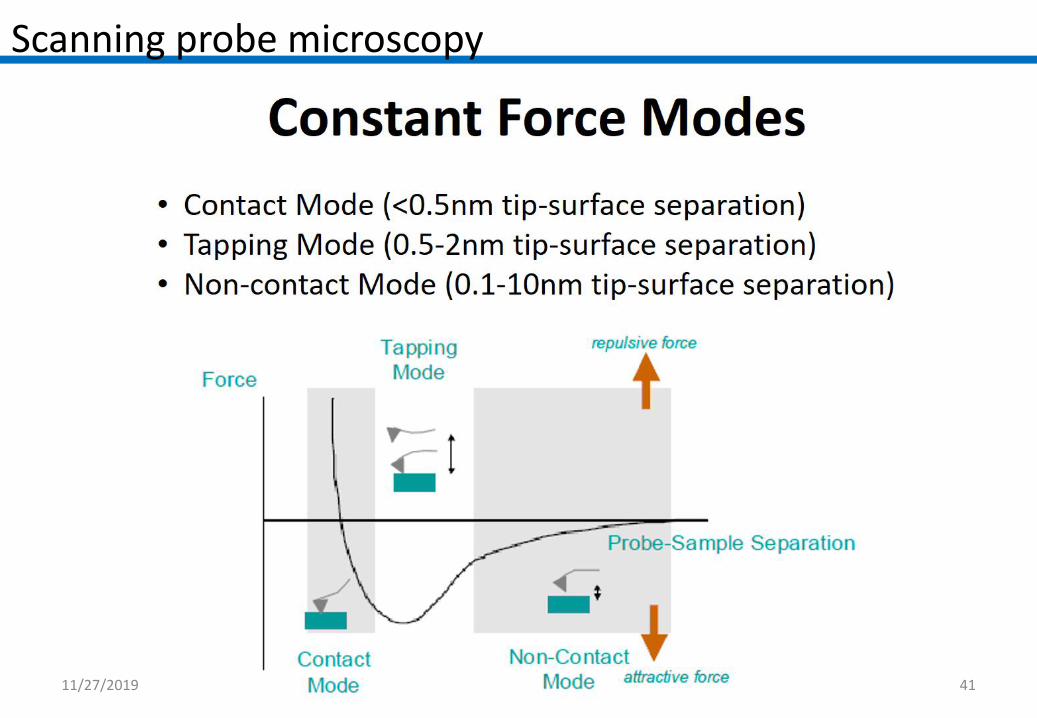
Scanning probe microscopy
11/27/2019 Nanotechnology and material science Lecture III
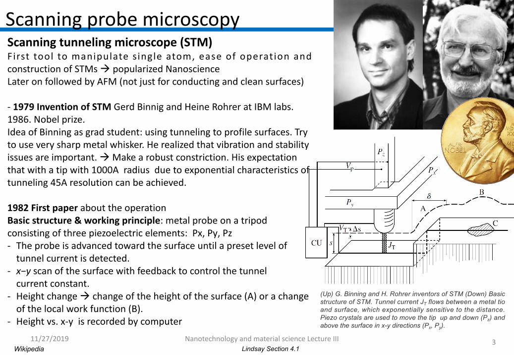
Scanning probe microscopyScanning tunneling microscope (STM)First tool to manipulate s ingle atom, ease of operation and construction of STMs popularized NanoscienceLater on followed by AFM (not just for conducting and clean surfaces)
- 1979 Invention of STM Gerd Binnig and Heine Rohrer at IBM labs. 1986. Nobel prize.Idea of Binning as grad student: using tunneling to profile surfaces. Try to use very sharp metal whisker. He realized that vibration and stability issues are important. Make a robust constriction. His expectation that with a tip with 1000A radius due to exponential characteristics of tunneling 45A resolution can be achieved.
1982 First paper about the operation Basic structure & working principle: metal probe on a tripod consisting of three piezoelectric elements: Px, Py, Pz- The probe is advanced toward the surface until a preset level of
tunnel current is detected.- x−y scan of the surface with feedback to control the tunnel
current constant. - Height change change of the height of the surface (A) or a change
of the local work function (B).- Height vs. x-y is recorded by computer
Lindsay Section 4.1
(Up) G. Binning and H. Rohrer inventors of STM (Down) Basic structure of STM. Tunnel current JT flows between a metal tio and surface, which exponentially sensitive to the distance. Piezo crystals are used to move the tip up and down (Pz) and above the surface in x-y directions (Px, Py).
3Wikipedia

11/27/2019 Nanotechnology and material science Lecture III
Scanning probe microscopy
Lindsay Section 4.1
(Middle) Fie sturcutre of the STM tip contains a single atom at the vry and of the tip. Since tunnel current is dominantlycoming from this atom ensures the atomic resolution. (Down) First image of the surface reconstrction of silicon (111) surface. First direct observation of this structure at the atomic level. IBM.
4Wikipedia
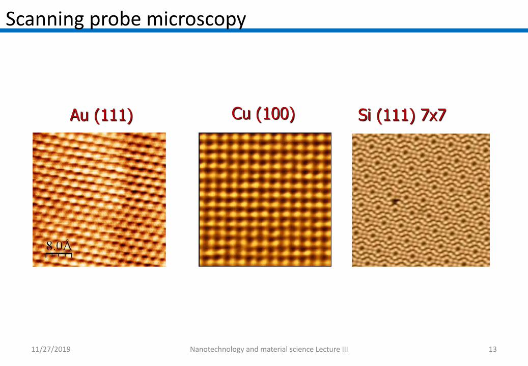
Scanning tunneling microscope (STM)First test of Au surface was a surprise, atomic terraces were measured (height 3A) Probe is not a sphere but a single atom dangling from the very tip! Atomic resolution
- The first image of the silicon 7 × 7 surface reported in the 1983 paper. At this early stage even IBM Corp. had not successfully attached a computer to a scanning probe microscope, so this three-dimensional rendition was made by cutting up copies of traces made on an x−y chart recorder, stacking them together, and gluing them!
First setup is complicated : magnetic levitation of a superconductor to provide vibration isolationFew generations later STM mechanism became so small, compact, and rigid that it was easily capable of atomic resolution when operated on a tabletop.Advantages:- STM can work without vacuum (not like SEM) and also in water- Cheap few kEUR widely used, big momentum to Nanotechnology

11/27/2019 Nanotechnology and material science Lecture III
Scanning probe microscopy
Lindsay Section 4.1
(Middle) Atomic strucutre of the STM tip contains a single atom at the very and of the tip. Since tunnel current is dominantly coming from this atom ensures the atomic resolution. (Down) First image of the surface reconstruction of silicon (111) surface. First direct observation of this structure at the atomic level. IBM.
5Wikipedia
Scanning tunneling microscope (STM)First test of Au surface was a surprise, atomic terraces were measured (height 3A) Probe is not a sphere but a single atom dangling from the very tip! Atomic resolution
- The first image of the silicon 7 × 7 surface reported in the 1983 paper. At this early stage even IBM Corp. had not successfully attached a computer to a scanning probe microscope, so this three-dimensional rendition was made by cutting up copies of traces made on an x−y chart recorder, stacking them together, and gluing them!
First setup is complicated : magnetic levitation of a superconductor to provide vibration isolationFew generations later STM mechanism became so small, compact, and rigid that it was easily capable of atomic resolution when operated on a tabletop.Advantages:- STM can work without vacuum (not like SEM) and also in water- Cheap few kEUR widely used, big momentum to Nanotechnology
11/27/2019 Nanotechnology and material science Lecture III
Scanning probe microscopy
Lindsay Section 4.1 6
Wikipedia
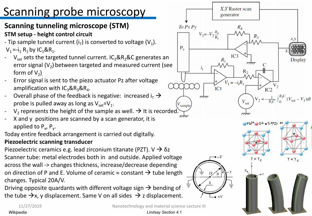
Scanning tunneling microscope (STM)STM setup - height control circuit - Tip sample tunnel current (iT) is converted to voltage (V1). V1 =-i1 R1 by IC1&R1. - Vset sets the targeted tunnel current. IC2&R2&C generates an
error signal (V2) between targeted and measured current (see form of V2).
- Error signal is sent to the piezo actuator Pz after voltage amplification with IC3&R3&R4.
- Overall phase of the feedback is negative: increased iT probe is pulled away as long as Vset=V1.
- V2 represents the height of the sample as well. It is recorded.- X and y positions are scanned by a scan generator, it is
applied to Px, Py.Today entire feedback arrangement is carried out digitally.Piezoelectric scanning transducerPiezoelectric ceramics e.g. lead zirconium titanate (PZT). V δzScanner tube: metal electrodes both in and outside. Applied voltage across the wall -> changes thickness, increase/decrease depending on direction of P and E. Volume of ceramic constant tube length changes. Typical 20A/V. Driving opposite quardants with different voltage sign bending of the tube x, y displacement. Same V on all sides z displacement.

11/27/2019 Nanotechnology and material science Lecture III
Scanning probe microscopy
Lindsay Section 4.1, and Appendix D. also E. Meyer: Scanning Probe Microscopy Springer (2004) Sec. 1.2.3
(Down) Mechanical transfer function of an STM system. T3 is the transfer function of STM with resonance frequency of 1kHz, T1 and T2 two damping system e.g. springs, several heavy metal plates with viton rings between, etc., which protect the system from external mechanical noises. Goal is to filter out noises above a few Hz. The total transfer function (T) fulfils this requirement.
7Wikipedia
Scanning tunneling microscope (STM)Speed limit of STM response – constant current modeTypical piezoelectric scanning elements have an intrinsic mechanicalresonant frequencies 1 - 50 kHz. Limitation on the fastest possible response of the microscope. If drive freq > resonance freq. 180 phase shift in response feedback loop gets unstable. Integrator part has to be sufficiently slow, tuned by R2 and C values. Shortest time to measure one pixel ~20usec.
This operation mode is the constant current mode. It provides safe operation with low risk to crash the tip. (typical tip distance 4-7A)Other mode: constant height mode. Scanning in X-Y direction at fixed height, measuring iT. Faster, no need for feedback. But thermal drifts, crashing risk.
Mechanical isolationSTM is very sensitive to acoustic noises. Mechanical noise transfer characteristics of STMs (see T3 on the figure) gets suppressed as f 0Hz. Mid freq. range has to be filtered out. Solution: Isolation systems with low resonance frequency. As Eq. 1 shows when ω >> ω0, the response of the system gets suppressed ~ ω-2.Various acoustic isolation systems: box, mechanical springs, heavy plates with Viton rings between, eddy currents, rubber feet, pendulum etc.
(Up) Amplitude (see also equation bellow) and phase response of a damped harmonic oscil lator when harmonic excitat ion with frequency, ω is applied. For Q=ω0 τ=10. ω0 is the resonance frequency, τ is the friction coefficient.

11/27/2019 Nanotechnology and material science Lecture III
Scanning probe microscopy
Lindsay Section 4.1, and Appendix D. also E. Meyer: Scanning Probe Microscopy Springer (2004) Sec. 1.2.3
(Down) Mechanical transfer function of an STM system. T3 is the transfer function of STM with resonance frequency of 1kHz, T1 and T2 two damping system e.g. springs, several heavy metal plates with viton rings between, etc., which protect the system from external mechanical noises. Goal is to filter out noises above a few Hz. The total transfer function (T) fulfils this requirement.
8Wikipedia
Scanning tunneling microscope (STM)
Speed limit of STM responseTypical piezoelectric scanning elements have an intrinsic mechanicalresonant frequencies 1 - 50 kHz. Limitation on the fastest possible response of the microscope. If drive freq > resonance freq. 180 pahse shift in response feedback loop gets unstable. Integrator part has to be sufficiently slow, tuned by R2 and C values. Shortest time to measure one pixel ~20usec.
Mechanical isolationSTM is very sensitive to acoustic noises. Isolation system. Mechanical noise transfer chracteristics of STMs (see T3 on the figure) gets suppressed as f 0Hz. Mid freq. range has to be filtered out. Solution: Isolation systems with low resonance frequency. As Eq. 1 shows when ω >> ω0, the response of the system gets suppressed ~ ω-
2.Various acustic isolation systems: box, mechanical springs, heavy plates with viton rings between, eddy currents, rubber feet, pendulum, silent room etc.
(Up) Amplitude (see also equation bellow) and phase response of a damped harmonic oscillartor when harmonic excited with frequency, ω is applied. For Q=ω0 τ=10. ω0 is the resonance frequency, τ is the friction coefficient.
11/27/2019 Nanotechnology and material science Lecture III 9
Scanning probe microscopy
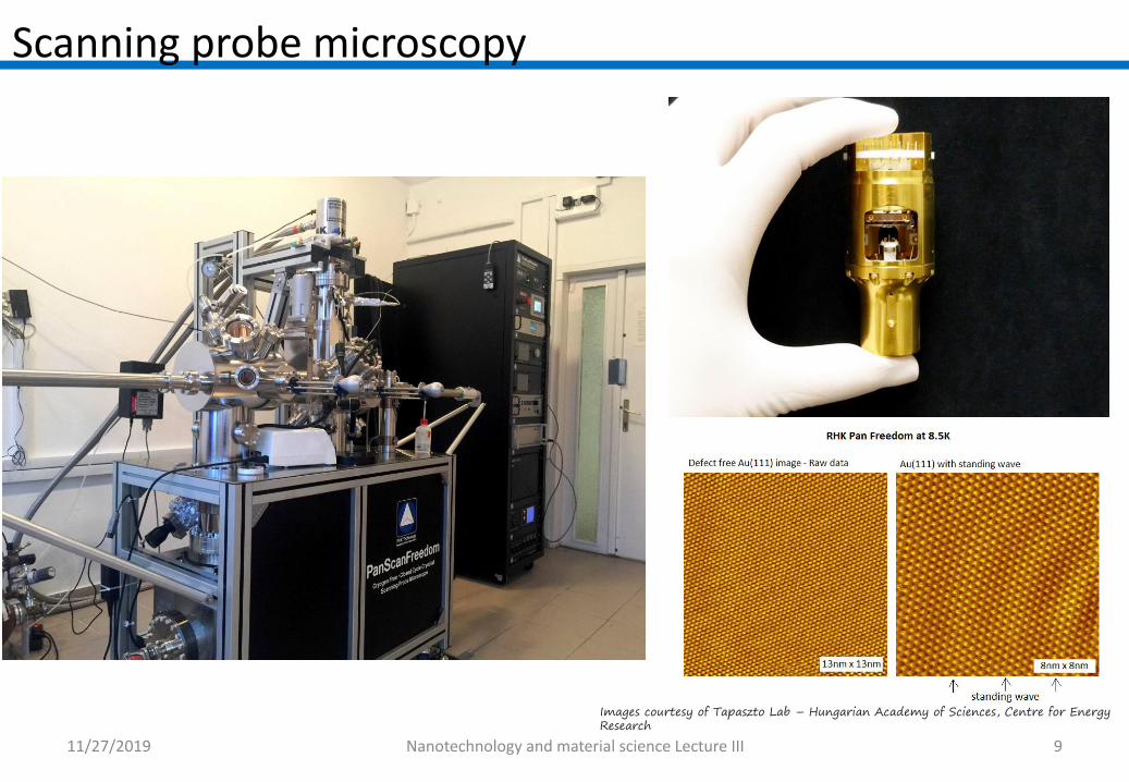
Images courtesy of Tapaszto Lab – Hungarian Academy of Sciences, Centre for Energy Research
11/27/2019 Nanotechnology and material science Lecture III 10
Scanning probe microscopy

11/27/2019 Nanotechnology and material science Lecture III
Scanning probe microscopy
Lindsay Section 4.1, and E. Meyer: Scanning Probe Microscopy Springer (2004) Sec. 2.1.11
Scanning tunneling microscope (STM)Basics of tunnel currentThe tunnel current can be calculated by Fermi’s golden rule:
where ρS, ρt are sample (S) and tip (t) DOS, and T is the tunneling transition probability:
where m is electron mass, S is the width of tunnel barrier, and (φS+ φT)/2 = φ is an average workfunction of S and t, V is the biasbetween S and t. T is calculated from according to quantum mechanics, how a particle with energy E can penetrate a barrier φ > E. (See Fig.) If we assume that V<< φ, and the DOS of the tip is flat:
Tunnel current depends exponentially on the tip sample distance S, and also influenced by energy dependent DOS of the sample. If ρS is constant in the eV window:
where φ is the workfunction in eV, z is the barrier width in Å. For a typical barrier height e.g. for Au φ=5eV tunnel current decays by factor
of 10 when spacing is changed by 1Å. See Tersoff-Hamann Model for more detail.
(Up) Energy diagram for tunneling . V voltage is applied between sample and tip, which are separated by a vacuum barrier with height of φ. The wave function of e penetrates into the barrier accoriding to the formula.
(1)

Scanning probe microscopyexact perturbative
11/27/2019 Nanotechnology and material science Lecture III 1313
Scanning probe microscopy

11/27/2019 Nanotechnology and material science Lecture III
14
Scanning probe microscopy
Graphene
Graphite
11/27/2019 Nanotechnology and material science Lecture III 15
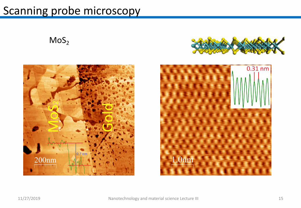
MoS2
Scanning probe microscopy
11/27/2019 Nanotechnology and material science Lecture III 16
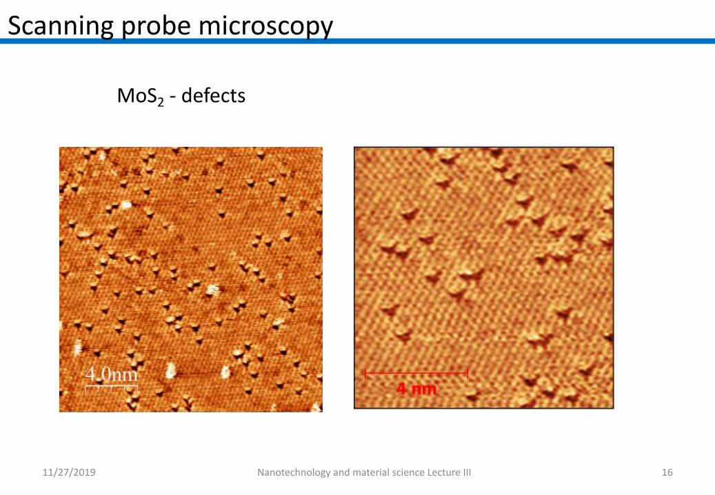
MoS2 - defects
Scanning probe microscopy

11/27/2019 Nanotechnology and material science Lecture III 17
MoS2 – defects – O saturation
Scanning probe microscopy

11/27/2019 Nanotechnology and material science Lecture III 1818
MoS2 - defects
Scanning probe microscopy
11/27/2019 Nanotechnology and material science Lecture III 19
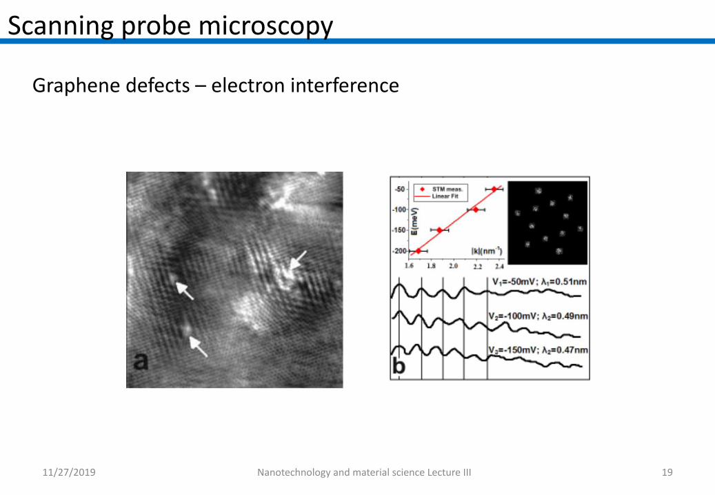
Graphene defects – electron interference
Scanning probe microscopy

11/27/2019 Nanotechnology and material science Lecture III 20
Graphene nanoribbon – electron interference
Scanning probe microscopy
11/27/2019 Nanotechnology and material science Lecture III 21
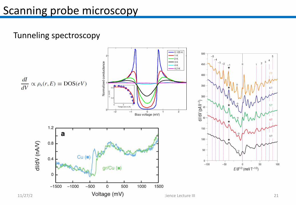
Tunneling spectroscopy
Scanning probe microscopy

11/27/2019 Nanotechnology and material science Lecture III 22
Scanning probe microscopy
MoS2 single layer bandgap –effect of strain

11/27/2019 Nanotechnology and material science Lecture III 23
Scanning probe microscopy
MoS2 single layer bandgap –effect of grain boundaries
11/27/2019 Nanotechnology and material science Lecture III 24
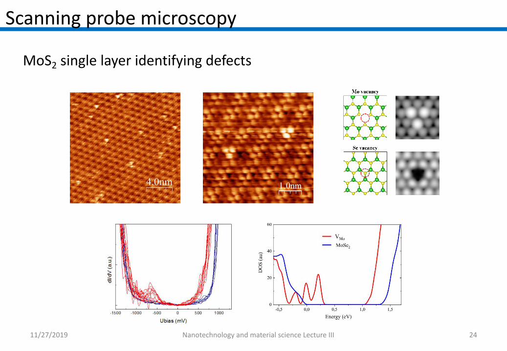
Scanning probe microscopy
MoS2 single layer identifying defects

11/27/2019 Nanotechnology and material science Lecture III 25
Scanning probe microscopy
Hunting electronic states

11/27/2019 Nanotechnology and material science Lecture III
Scanning probe microscopy
26
Scanning tunneling microscope (STM)Scanning tunneling spectroscopy (STS)
Example 3: Mapping of Homo or Lumo orbital of a molecule when bias reaches their energyIn case of elastic tunneling current increases linearly. At a treshold an additional current channel opens up. The origin: when electron has enough energy to excite a vibration mode i.e. eV > ħω, an inelastic channel opens where during tunneling a phonon is created. Panel d shows the typical I – V curves with a characteristic kink. ITS signal is usually very small Better to use d2I/dV2. It results a peak at the vibrational energy.
ITC can be used to chracterize a molecule on the surface. See example bellow. Isotope effect is often used as a further experimental check.
E. Meyer: Scanning Probe Microscopy Springer (2004) Sec. 2.2.
(Right) First observation of ITS of acetylene molecule on Cu (100) surface. (a) I-V on the molecule (1) and on Cu surface (2) and their difference.(1-2) (b) Peak at 358 eV corresponds to the C-H stratching mode of the molecule. B.C. Stripe Science 280, 1732 (1998)
Recent advances in submolecular resolution with scanning probe microscopyLeo Gross, Nature Chemistry 3, 273–278 (2011) doi:10.1038/nchem.1008
a and b spatial resolved HOMO and LUMO orbitals and corresponding calculations (c),
(d). e and f ar NC-AFM images with CO functionalized tip.

11/27/2019 Nanotechnology and material science Lecture III
Scanning probe microscopy
E. Meyer: Scanning Probe Microscopy Springer (2004) Sec. 2.2.27
Scanning tunneling microscope (STM)Manipulation modeVertical and lateral manipulations
Vertical manipulationa) transfer of the surface atom to the tip.b) Tip is moved to the desired position. c) Deposition Transfer of the adsorbate atom from the surface tothe tip, or vice versa, is achieved by bringing the tip close and applying voltage pulse. E.g. Xe atoms moves same direction as tunneling electrons due to heat assisted electromigration.
Lateral manipulationa) Tip is moved down a few Å, set point is increased b) Tip forms a weak bond with the adsorbate atom or molecule. c) Tip is then moved along the line of manipulation. Typical threshold resistances to slide an adsorbate are 5k-20kΩ. Tip height during manipulation can be recorded, which gives some insight about the manipulation process.See example: e.g. Cu adatoms are shifted sites by sites (a), Pb dimmer (e-g) can jump several sites, since it is larger object.
Other mechanisms: field assisted direction diffsuion, inelastic tunneling induced movement for H adatoms
(Up) Arranged 48 iron atoms on the surface of a copper substrate. These images show the various stages of the process. Once complete the circular arrangement of the iron atoms it forces the electrons at the surface of the copper to specific quantum states as shown by the rippled appearance of the surface. By Don Eigler IBM. (Down) Tip height curves during lateral manipulation of various atoms on the Cu(211)surface. The tip movement is from left to right, the fixed tunneling resistances are indicated. Vertical dotted lines correspond to fcc sites next to the step edge.

11/27/2019 Nanotechnology and material science Lecture III 28
Scanning probe microscopy
STM lithography of graphene
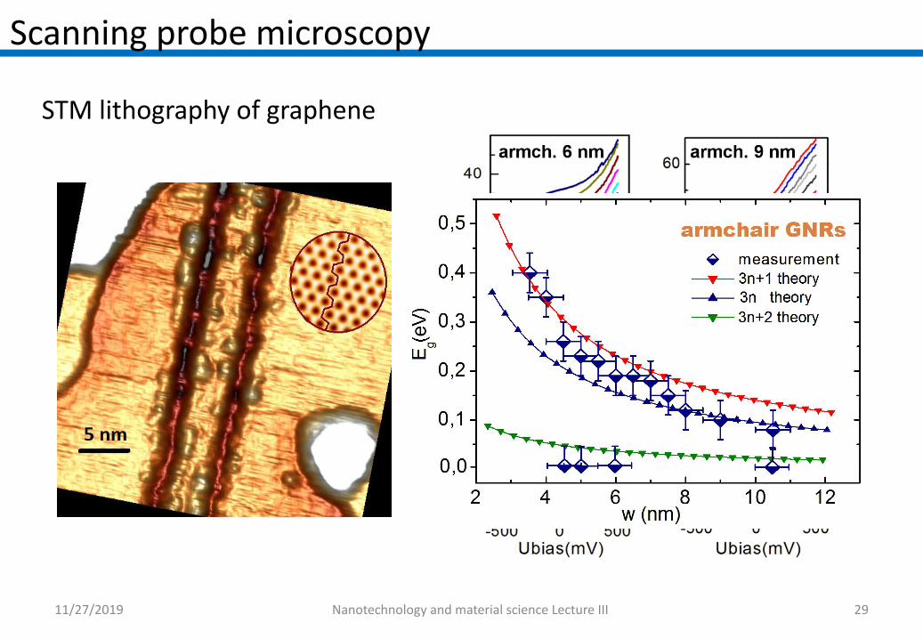
11/27/2019 Nanotechnology and material science Lecture III 29
Scanning probe microscopy
STM lithography of graphene

11/27/2019 Nanotechnology and material science Lecture III 30
Scanning probe microscopy
STM lithography of graphene

11/27/2019 Nanotechnology and material science Lecture III 31
Scanning probe microscopy

11/27/2019 Nanotechnology and material science Lecture III 32
Scanning probe microscopy
11/27/2019 Nanotechnology and material science Lecture III 33
Scanning probe microscopy
11/27/2019 Nanotechnology and material science Lecture III 34
Scanning probe microscopy
11/27/2019 Nanotechnology and material science Lecture III 35
Scanning probe microscopy
11/27/2019 Nanotechnology and material science Lecture III 36
Scanning probe microscopy

11/27/2019 Nanotechnology and material science Lecture III 37
Scanning probe microscopy

11/27/2019 Nanotechnology and material science Lecture III 38
Scanning probe microscopy
11/27/2019 Nanotechnology and material science Lecture III 39
Scanning probe microscopy

11/27/2019 Nanotechnology and material science Lecture III 40
Scanning probe microscopy
11/27/2019 Nanotechnology and material science Lecture III 41
Scanning probe microscopy

11/27/2019 Nanotechnology and material science Lecture III 42
Scanning probe microscopy

11/27/2019 Nanotechnology and material science Lecture III 43
Scanning probe microscopy
11/27/2019 Nanotechnology and material science Lecture III 44
Scanning probe microscopy

11/27/2019 Nanotechnology and material science Lecture III 45
Scanning probe microscopy

11/27/2019 Nanotechnology and material science Lecture III 46
Scanning probe microscopy

11/27/2019 Nanotechnology and material science Lecture III 47
Scanning probe microscopy

11/27/2019 Nanotechnology and material science Lecture III 48
Scanning probe microscopy

11/27/2019 Nanotechnology and material science Lecture III 49
Scanning probe microscopy
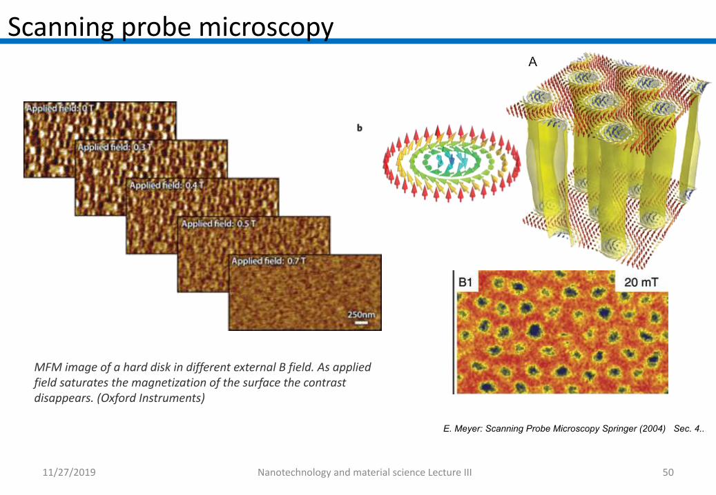
11/27/2019 Nanotechnology and material science Lecture III 50
MFM image of a hard disk in different external B field. As applied field saturates the magnetization of the surface the contrast disappears. (Oxford Instruments)
E. Meyer: Scanning Probe Microscopy Springer (2004) Sec. 4..
Scanning probe microscopy

11/27/2019 Nanotechnology and material science Lecture III 51
Near-Field Scanning Optical Microscopy (NSOM)
Break the diffraction limit by working in the near-field
Launch light through small aperture
Illuminated “spot” is smaller than diffraction limit
(about the size of the tip for a distance equivalent to tip
diameter) Near-field = distance of a couple of tip diameters

11/27/2019 Nanotechnology and material science Lecture III 52
How to move the tip? Steal from AFM

11/27/2019 Nanotechnology and material science Lecture III 53
The light source is usually a laser focused into an optical fiber through a polarizer, a beam splitter and a coupler.
The scanning tip is usually a pulled or stretched optical fiber coated with metal except at the very tip or just an AFM cantilever with a hole in the center of the pyramidal tip.
Standard optical detectors, such as avalanche photodiodes, photomultiplier tubes (PMT) or CCD, can be used.
Single molecules of DiI on glass surface
Scanning probe microscopy