characterization methods and instruments
TRANSCRIPT
46
Chapter 3
Characterization Methods and Instruments
3.1 Introduction
Characterization is the key link for understanding how the microstructure, chemical
composition and structure of PCD specimens and polishing debris are related to their
polishing conditions, the chemical reactions of PCD at elevated temperatures and the
material removal mechanisms.
This chapter will introduce the various techniques which were used in our experiments
to characterize the polished/unpolished PCD specimens, polishing-produced debris and
temperatures of PCD surface in polishing. Some of the techniques are suitable for trace
identification and others for determination of the chemical structures and phases. By
combined use of the characterization methods, the surface quality and microstructure,
chemical composition and structure of the polished/unpolished specimens can be
determined. The morphology, elemental composition, chemical structure and atomic
bonding of polishing debris can be identified. Additionally, the polishing surface
temperature due to frictional heating can be determined so that the chemical reactions at

47
elevated temperature and the material removal mechanism during polishing can be
discovered. An attempt will then be made to control and optimize polishing conditions.
In each of the techniques, the advantages and their limitations are considered, and then
their usefulness in determining the PCD surfaces quality, elements or structure in PCD
specimens and polishing debris is also presented. In addition, the details of instruments
used in our experiments are illustrated along with the instrument pictures. Finally, the
principle of thermocouple, its selection for different applications and some precautions
and considerations for using thermocouples for reducing error in our on-line
temperature measurement are discussed.
3.2 Examination of Surface Topography and Roughness
3.2.1 Optical Microscopy
An optical microscope is essentially an extension of our own eyes, and it enables us to
directly view structures that are below the resolving power of the human eye (0.1 mm)
[Brundle et al., 1992]. Optical microscopic techniques are essential for the study of the
PCD specimen surface before and after polishing. It can be used to determine diamond
grain condition and general surface topography in low magnification before polishing,
and to investigate the adhered layer, cracks, degree of polishing and surface quality after
polishing. The scale of investigations is limited by the resolution of the optical
instruments and the depth of focus. The low magnification provides the possibility of
studying large fields of PCD surface directly. The technique is efficient for general
surface quality, surface topography of the adhesive layer, grain size determination,
48
location and morphology of cracks. Optical microscopy is considered as the first step in
the study of the microstructure of the PCD specimen.
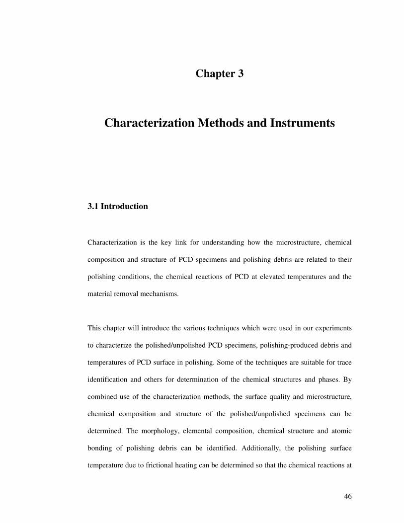
Figure 3.1 illustrates the optical microscope (Leica DM RXE), which was used to
characterize the microstructure of the PCD specimen surface. The magnifications used
were 50, 100, 200, and 500 times. The images were taken by a digital camera and
transferred to a computer where they were analysed using program, Leica Qwin. It was
mainly used for examining the microstructure of the PCD specimens before and after
polishing, and documents the progress of polishing experiments.
Fig. 3.1 Leica DM RXE microscope
3.2.2 SEM and EDX
Scanning Electron Microscopy (SEM) is a powerful and versatile method for the
characterization of the details of the specimen surface [Brundle et al., 1992, Rutledge
and Gleason, 1997, Zarudi, 1998]. In SEM, the specimen is examined by a focused
electron beam. The application of the electron permits one to get a much higher

49
resolution compared with optical microscopy. The magnification in SEM used in our
experiments can range from 10 to 10,000 times. SEM also has a big depth of focus that
enables having a quality image of the surface with rough topography. This wide range
of magnifications and big depth of focus make the study of specimen surfaces and
polishing debris convenient. Regions of special interest can be recognized easily under
small magnification, and followed by further precise studies with higher magnification.
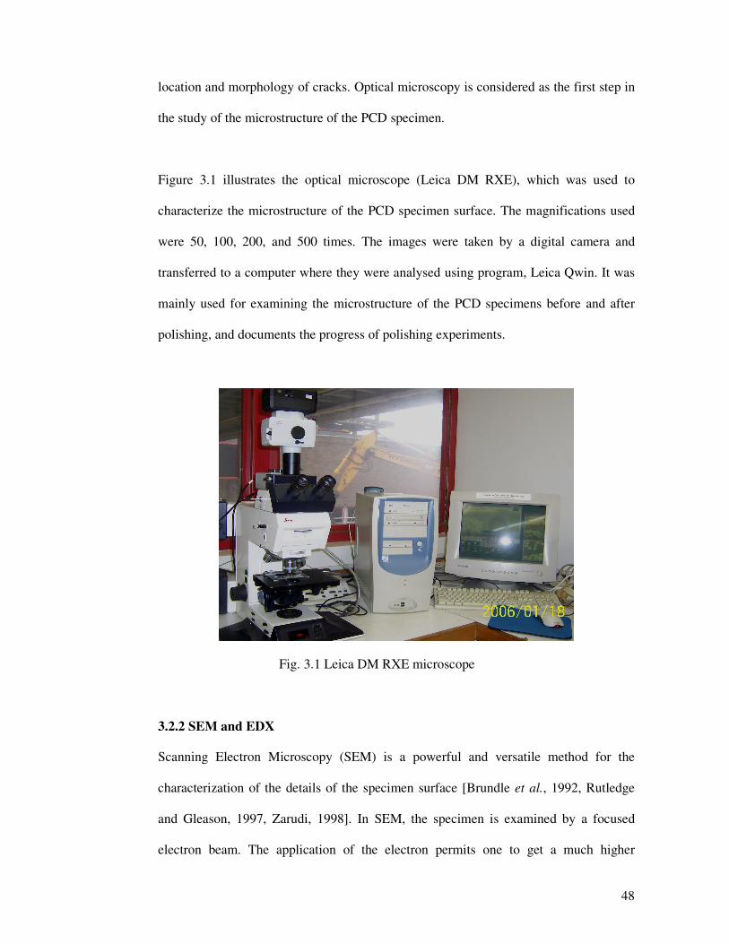
The application of SEM provides detailed information of the specimen surface with
either secondary or backscattered electrons or both. Backscattered electrons are primary
beam electrons which have been elastically scattered by nuclei in the sample and escape
from the surface. Backscattered electrons have high energy (greater than 50 eV) and
they can come from depths of 1 µm or more within the specimen. Since they result from
elastic scattering events, signals from regions containing high elements appear brighter,
thus providing a SEM image with topographic contrast. Secondary electrons with
average energy 5 eV come from a region very close to the surface. Therefore the limited
escape depth of the lower energy secondary electrons provides higher surface sensitivity
images. Figure 3.2 shows the backscattered and secondary electron images of a polished
PCD specimen. From the figures, it can be seen that secondary images could provide
more detailed information on smooth specimen surfaces. Thus in our SEM experiment,
most micrographs of polished specimens were recorded in secondary images. However,
a backscattered image could provide more information on rough surface, so some of the
specimen images before polishing are backscattered.
50
(a) Backscattered image
(b) Secondary image
(c) Backscattered image
(d) Secondary image
Fig 3.2 SEM images of polished PCD specimen
Additional information can be obtained with an Energy Dispersive X-ray Spectrometer
(EDX), which permits the study of the chemical composition of interested areas on the
surface. EDX analyses the energy of X-ray produced during the relaxation of a
particular excited specimen atom when the electron beam knocks out inner K, L, M
shell electrons. Figure 3.3 shows a schematic of an EDX system on an electron column
[Brundle et al., 1992]. The incident electron interacts with the specimen with the
emission of X rays. These X rays pass through the window protecting the Si (Li) and are
absorbed by the detector crystal. The X-ray energy is transferred by a field effect
transistor (FET), and amplified (AMP) to a level that can be processed into a digital

51
signal by the analog-to-digital converter (ADC) of the multichannel analyzer (MCA).
By an energy calibration of the channels in the MCA, the collection of X-ray pulses is
displayed as an energy histogram. EDX systems are controlled by computers and are
used for the basic operations of spectrum collection and peak identification. The X-ray
spectra give information on the types of elements present in a specimen from the
wavelength of the X-ray emitted and the elemental concentration from the intensity of
the particular peak.
Fig. 3.3 Schematic of an EDX system
Figure 3.4 shows the SEM Philips 505, which was used for studying the surface
topography and structure of the PCD specimens and polishing debris. At the same time,
EDX analysis was used to investigate the chemical compositions of the interested areas
or spots. By using SEM and its attached EDX analysis, the interested regions of PCD
specimens could be recognized easily under small magnification, and then could further
be precisely studied with higher magnification. On the interested areas or spots, the
chemical compositions could be detected by EDX. Also morphology of different
polishing debris could be observed under SEM, and their elemental compositions could
be identified to find out where the debris came from. This information of the elemental
Si(Li) FET AMP MCA Sample
e-
X-ray
Window
Display

52
compositions could be used for further X-ray diffraction (XRD), electron energy loss
spectroscopy (EELS) and Raman structure analyses.
Fig. 3.4 Philips SEM 505
3.2.3 Surface roughness tester
The surface roughness of unpolished and polished PCD surfaces was measured using a
surface roughness tester Surftest 402 and Surftest Analyzer from Mitutoyo (Fig.3.5).
Fig 3.5 Surface roughness tester and analyzer
Detector Driver unit Analyzer Leveled bench Printer

53
The machine consists of a detector, driving unit and analyzer. A diamond stylus
mounted at the end of the detector is in contact with the surface being measured and will
traverse for a specified distance. Signals obtained from the unit are transferred to the
analyzer for displaying or printing the result. Different roughness parameters, including
from filtered curves Ra, Rq, Rz, Rmax(DIN), Rt, Rp (R mode) and R3Z, and from
unfiltered Rz (JIS), Rz (JIS) and Rp (P mode) can be selected from the analyzer to
measure the surface roughness values by using this machine. Every traverse can only
measure and display one parameter. In the present research, the three common values
Ra, Rq, and Rmax were measured on a PCD specimen surface. Ra is the arithmetic
mean of the departures of the roughness profile from the mean line, while Rq (Rms) is
the root mean square corresponding to Ra, and Rmax is the maximum peak to valley
height within the sampling length.
To avoid vibration, the driver unit and the measuring specimen were placed on a
levelled steel table. Prior to the test, the accuracy of the instrument was checked and
calibrated by measuring a reference specimen. Measurements were made on several
positions of the PCD specimen.
3.2.4 Laser confocal microscopy
The Laser confocal microscopy permits obtaining precise information on a cross-section
of the PCD specimen surface without introducing distortion [Zarudi, 1998]. In confocal
imaging technique, a point light source is imaged on a specimen by a lens [Cox, 2003].
The light has to be collected with an objective lens and at the back focal plane of an
objective lens system, a small variable pinhole aperture (50~300 microns in diameter) is
positioned to exclude out of focus light from passing into the detector, as shown in the

54
schematic diagram Fig. 3.6. Light from the dotted red region is correctly focused by the
lens system and enters the pinhole aperture. However, the solid green and blue regions
are out of focus and are prevented from contributing to the image. Confocal operation
has the property of rejecting information from outside the plane of focus and in this way
providing the possibility of cross-sectioning without destroying the surface. The
resolution in the vertical direction can be 0.1 µm. In practice, the confocal microscopy
is capable of exploration of details of the surface up to 0.5 µm in height.
Lens Pinhole
apertureFocal plane
Fig 3.6 Schematic diagram of confocal principle
The PCD surface topographic parameters, including the radius of asperity summits,
surface density of asperities and spread of asperity heights, were measured by using a
BIO-RAD MRC-600 laser scanning confocal microscope, as shown in Fig.3.7.

55
Fig.3.7 BIO-RAD MRC-600 confocal microscope
With the confocal microscope, a series of pictures in focus on different layers can be
obtained. Also these pictures can be compiled to an extended focus image. Then on a
selected line, a surface roughness diagram can be acquired to generate surface
roughness data, from which the spread of asperity heights can be determined by using a
statistical data analysis tool. Using the microscopy analysis software LEICA QWin,
these extended focus images were analysed. From the results of the asperity field
analysis, the area of asperity, the number of asperities (count), the total area of analysed
frame and the ratio of counts to frame area can be obtained. These experimental data
were used for estimating the temperature rise at the polishing interface of the PCD
asperities and polishing metal disk (details will be discussed in Chapter 6).
3.2.5 AFM
Atomic force microscopy (AFM) is used to obtain information from surfaces with the
possibility of atomic resolution [Hird, 2002, Zarudi, 1998]. In this technique, a sharp tip
(radius nominally 300 Å) is mounted upon a cantilever spring and brought into contact
with a sample. The vertical displacement due to attractive and repulsive forces between
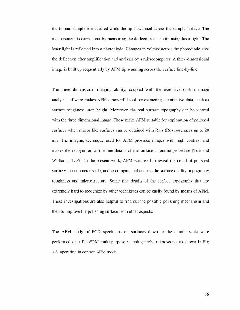
56
the tip and sample is measured while the tip is scanned across the sample surface. The
measurement is carried out by measuring the deflection of the tip using laser light. The
laser light is reflected into a photodiode. Changes in voltage across the photodiode give
the deflection after amplification and analysis by a microcomputer. A three-dimensional
image is built up sequentially by AFM tip scanning across the surface line-by-line.
The three dimensional imaging ability, coupled with the extensive on-line image
analysis software makes AFM a powerful tool for extracting quantitative data, such as
surface roughness, step height. Moreover, the real surface topography can be viewed
with the three dimensional image. These make AFM suitable for exploration of polished
surfaces when mirror like surfaces can be obtained with Rms (Rq) roughness up to 20
nm. The imaging technique used for AFM provides images with high contrast and
makes the recognition of the fine details of the surface a routine procedure [Tsai and
Williams, 1995]. In the present work, AFM was used to reveal the detail of polished
surfaces at nanometer scale, and to compare and analyse the surface quality, topography,
roughness and microstructure. Some fine details of the surface topography that are
extremely hard to recognize by other techniques can be easily found by means of AFM.
These investigations are also helpful to find out the possible polishing mechanism and
then to improve the polishing surface from other aspects.
The AFM study of PCD specimens on surfaces down to the atomic scale were
performed on a PicoSPM multi-purpose scanning probe microscope, as shown in Fig
3.8, operating in contact AFM mode.
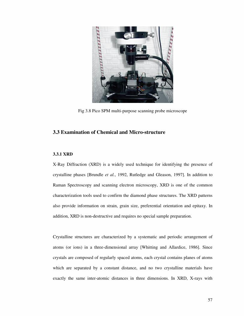
57
Fig 3.8 Pico SPM multi-purpose scanning probe microscope
3.3 Examination of Chemical and Micro-structure
3.3.1 XRD
X-Ray Diffraction (XRD) is a widely used technique for identifying the presence of
crystalline phases [Brundle et al., 1992, Rutledge and Gleason, 1997]. In addition to
Raman Spectroscopy and scanning electron microscopy, XRD is one of the common
characterization tools used to confirm the diamond phase structures. The XRD patterns
also provide information on strain, grain size, preferential orientation and epitaxy. In
addition, XRD is non-destructive and requires no special sample preparation.
Crystalline structures are characterized by a systematic and periodic arrangement of
atoms (or ions) in a three-dimensional array [Whitting and Allardice, 1986]. Since
crystals are composed of regularly spaced atoms, each crystal contains planes of atoms
which are separated by a constant distance, and no two crystalline materials have
exactly the same inter-atomic distances in three dimensions. In XRD, X-rays with

58
wavelength, λ, between 0.5 and 2Å are impinged upon a sample. The diffracted X-rays
are measured at 2θ, the angle between the X-ray source and detector. The diffraction
can then be described by Bragg’s law
λ=2d(hkl) sin θ, (3.1)
where d(hkl) is the spacing between atomic planes within the sample. The relative
intensity of a diffraction peak from a given set of planes can be determined by using the
symmetry of the lattice to calculate a structure factor [Rutledge and Gleason, 1997].
One of the most important uses of XRD is phase identification. This is achieved by
comparing the measured d-spacing in the diffraction pattern and their integrated
intensities with known standards in the JCPDS (Joint Committee on Powder Diffraction
Standards) Powder Diffraction File [Brundle et al., 1992].
Fig. 3.9 XRD Siemens D5000 X-ray
A study of the crystal structure of the PCD specimens and polishing debris were
performed on a XRD Siemens D5000 X-ray diffractometer, shown in Fig.3.9. The
specimen stage could hold powder or solid specimens. The data were collected on the
D5000 X-ray diffractometer. The diffraction data file was displayed and treated by the
59
EVA program which permitted a search and match directly into the JCPDS database. A
series of peak positions could be characteristic for crystal faces. If the elements of the
specimen are already known (e.g. from EDX analysis), the search and match could be
limited to the known elements structures. The most intense lines in the diffractograms
were assigned to known compounds by means of a procedure for searching for and
matching with, lines of known crystalline compounds in the database.
By using the XRD to analyse the chemical structures of polishing debris, PCD
specimens and the polishing metal disk tool before and after polishing, the chemical
reactions during polishing can be identified and the material removal mechanisms can
be found.
However, though XRD can provide information on crystalline structure, diffraction
from semicrystalline and amorphous materials is very weak; the diffraction pattern may
consist of broad features or halos on thick specimens or synchrotron radiation [Brundle
et al., 1992]. Normally, a non-crystalline structure, like amorphous carbon will not give
rise to a XRD pattern [Rutledge and Gleason, 1997]. Thus the possibility of
carbonization of diamond during polishing cannot be confirmed by XRD. Another
technique, Raman spectroscopy, which can distinguish between different forms of
carbon, was applied to further investigate the polishing debris and the PCD specimen
and find out the material removal mechanisms.
3.3.2 Raman spectroscopy
Raman spectroscopy has emerged as one of the principal characterization methods for
diamond materials because of its ability to distinguish between different forms of

60
carbon [Bonnot, 1990, Johnston et al., 1992, Knight and White, 1989, Rutledge and
Gleason, 1997, Solin and Ramdas, 1970]. Raman spectra can provide a large amount of
structural and phase information about carbon. Also Raman spectroscopy is non-
destructive and requires no special preparation of specimens, and the spectrum is little
affected by admixture with other species. Moreover, the position of any particular
Raman band is sensitive to temperature, pressure/stress, and finite crystal size [Johnston
et al., 1992].
Raman spectroscopy relies on the analysis of a small fraction of the incident light
impinging on a sample being inelastically scattered by interaction with the lattice
vibrations of the material being investigated. An intense monochromatic light beam
impinges on the sample; the scattered beam is reradiated in all directions [Brundle et al.,
1992, Jasco, 2005]. The energies of the majority of the photons are unchanged by the
process, and are reradiated at the same frequency as that of the incident exciting light,
which is elastic or Rayleigh scattering. However, about one in one million photons or
less, lose or gain energy that corresponds to the vibrational frequencies of the scattering
molecules. This can be observed as additional peaks in the scattered light spectrum. The
process is known as Raman scattering and the spectral peaks with lower and higher
energy than the incident light are known as Stokes and anti-Stokes peaks respectively.
In practice, observed Raman spectra are almost always Stokes lines.
The Raman shifts are equivalent to the energy changes involved in transitions of the
scattering species and are therefore characteristic of it [Szymanski, 1967]. Each
scattering species gives its own characteristic vibrational Raman spectrum, which can
be used for its qualitative identification, and which is effective in studying its material
61
structure. In systems where chemical interaction occurs, the presence of new molecular
species can be detected by the appearance of new Raman lines. Moreover, since the
intensity of a characteristic Raman line is to give a fair approximation proportional to
the volume concentration of the species, Raman intensity measurements provide a basis
for quantitative analysis.
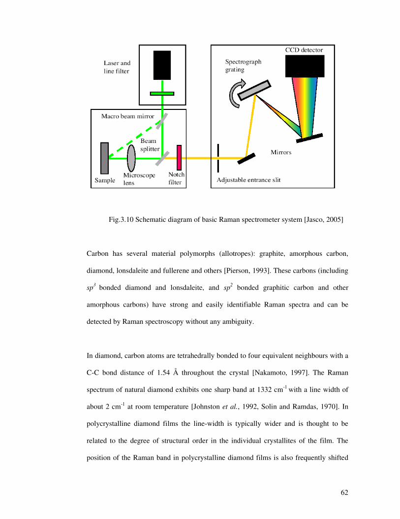
The basic components of a singly-dispersive Raman spectrometer system are shown in
Fig.3.10. The main system subcomponents are the laser light source, the microscope
sample chamber and the spectrograph [Jasco, 2005]. Laser light passes a line filter to
remove any unwanted lines before passing via Beam splitter into the Microscope.
Additional optics including a Macro beam mirror placed before the microscope, allow
macroscopic illumination of the sample. The sample scatters this light, which is
collected by the objective and passed back to the Beam splitter. This time, the light is
transmitted through the Beam splitter and passes the Rayleigh rejection Notch filter that
is used to eliminate the Rayleigh scattering. This is a narrow rejection-band filter that
strongly blocks light within ± 50 cm-1 of the laser wavelength from reaching the
spectrograph section. Then a spectrograph-grating system is used to effectively suppress
the stray light and provide a clean background for the Raman spectra. The charge-
coupled device (CCD) detector can collect a wide spectrum until good intensity is
obtained, and the data are processed and displayed by a computer.
62
Fig.3.10 Schematic diagram of basic Raman spectrometer system [Jasco, 2005]
Carbon has several material polymorphs (allotropes): graphite, amorphous carbon,
diamond, lonsdaleite and fullerene and others [Pierson, 1993]. These carbons (including
sp3 bonded diamond and lonsdaleite, and sp
2 bonded graphitic carbon and other
amorphous carbons) have strong and easily identifiable Raman spectra and can be
detected by Raman spectroscopy without any ambiguity.
In diamond, carbon atoms are tetrahedrally bonded to four equivalent neighbours with a
C-C bond distance of 1.54 Å throughout the crystal [Nakamoto, 1997]. The Raman
spectrum of natural diamond exhibits one sharp band at 1332 cm-1 with a line width of
about 2 cm-1 at room temperature [Johnston et al., 1992, Solin and Ramdas, 1970]. In
polycrystalline diamond films the line-width is typically wider and is thought to be
related to the degree of structural order in the individual crystallites of the film. The
position of the Raman band in polycrystalline diamond films is also frequently shifted

63
relative to that of natural diamond. This has been attributed to the presence of residual
stresses in the diamond films.
Lonsdaleite is known as hexagonal diamond. It is related to the 3C packing in cubic
diamond by the shift of one carbon layer along the 111 planes [Knight and White, 1989].
Although there are layers of carbon atoms in a 2H stacking, all carbons are 4
coordinated. Lonsdaleite is formed during the initial transformation of hexagonal
graphite into a final diamond, but retains graphite’s hexagonal crystal lattice. The
conversion path proceeds through a preliminary sliding of the graphite planes into an
orthorhombic stacking where an abrupt collapse and buckling of the planes leads to both
cubic and hexagonal (lonsdaleite) forms of diamond. It can also be obtained from
Wurtzite by replacing both the Zn and S atoms by carbon. The Raman spectra of
lonsdaleite exhibit a single broad band which varies in wavenumber between specimens.
Position of the maximum may range from 1311 to 1350 cm-1 and its full width at half
maximum (FWHM) may increase up from 40 cm-1 to 100 cm-1 [Zaitsev, 1997].
Three generally distinguishable types of sp2 carbon include crystalline graphite,
defective or microcrystalline graphite, and amorphous carbon [Rutledge and Gleason,
1997]. In single crystals graphite, sheet structures are formed by linking each carbon
atom to three equivalent neighbours in a trigonal planar fashion (C-C distance, 1.42 Å),
and all sheets parallel to each other with a distance of 3.35 Å [Nakamoto, 1997,
Tuinstra and Koenic, 1970]. The Raman spectrum of single crystals of graphite exhibits
only one band at 1575 cm-1 with width of 2 cm-1, while polycrystalline graphite shows
another band at 1355 cm-1. Disordered polycrystalline and non-crystalline graphitic
carbons exhibit two broad bands at 1355 and 1575 cm-1 [Knight and White, 1989].
64
These are the most diagnostic features and are designated the D band and G band,
respectively. Line width and D/G intensity ratio both vary depending on the structure of
the carbons. The widths of D and G bands correlate well with the degree of disorder
over the entire order-disorder carbon materials. The highly disordered carbons have
very broad bands whereas the lines are much narrower in crystalline structure. The
Raman spectra of amorphous carbon consist of distinctive broad asymmetric band
peaking at around 1500±40 cm-1 [Rutledge and Gleason, 1997].
In general, the defects composed of sp3 bonded carbon atoms are revealed in diamond
Raman scattering at frequencies < 1332 cm-1 [Zaitsev, 1997]. In contrast, the sp2
(graphitic) bonded species are revealed at > 1332 cm-1. The reason is that the sp2 carbon
bonds are stronger than the sp3 carbon bonds. The Raman intensity of the graphite (sp
2)
bonded carbon spectrum is more than 50 times that of the diamond (sp3) spectrum
[Knight and White, 1989, Zaitsev, 1997]. The Raman spectrum is a very effective
means of detecting percentage levels of graphitic carbon in diamond but is not a
sensitive test for diamond in the presence of other types of carbon.
In the present research, Raman spectroscopy is applied to analyse the PCD specimen
before and after polishing, and the polishing-produced debris. By analysing the Raman
spectra of the PCD specimens and polishing debris, different forms of carbon structure
can be found at different stages of the polishing process, the carbon phase
transformation can be detected and then the material removal mechanism can be
discovered.

65
Raman spectra were obtained using a Renishaw Raman Microscope (systems 2000)
with a CCD array detector shown in Fig.3.11. The collection optics were based on a
Leica DMLM microscope. The specimens or debris (in the form of powder) were placed
underneath the microscope objective (×5, 20, 50). The zones for the recording of
spectra were selected optically, and they were excited by an argon 514.5 nm Laser with
20 mW power directed through the microscope. The scattered light is collected (180°
degree backscattering) along the same optical path as the incoming laser.
Fig. 3.11 Renishaw Raman system
3.3.3 TEM and electron diffraction
Transmission electron microscopy (TEM) is one of the most powerful instruments for
investigating the microstructure of materials [Flewitt and Wild, 1994, Williams and
Carter, 1996a, Zarudi, 1998]. The fine details of microstructure can be examined in
specimens sufficiently thin to facilitate transmission of an electron beam without loss of
intensity. It is possible to achieve a resolution of 0.2 nm. In addition, many TEM
instruments have the capability of undertaking both physical and chemical analysis on
micro-areas of the specimen, e.g. EDX and electron diffraction, and some with electron
energy loss spectroscopy (EELS).
66
EDX analyses could give information on the types of elements present in a specimen
and on the elemental concentration from the intensity of the particular peak, and also on
the elemental distribution mapping.
TEM can provide very high magnification (>106) images and electron diffraction
patterns from the same sample [Rutledge and Gleason, 1997]. The image is obtained in
a direct or diffracted beam, giving information about the crystallographic structure.
When a beam of electrons is incident on the top surface of a thin crystalline electron
microscope specimen, specific diffracted beams arise at the bottom exit surface
[Edington, 1975, Williams and Carter, 1996b]. Although each individual atom in the
crystal scatters the incidence beam, the scattered wavelets will only be in phase (that is
reinforced) in particular crystallographic directions. Electron diffraction patterns can be
used to gain quantitative information on the identity of phases and their orientation
relationship to the matrix, and exact crystallographic descriptions of crystal defects
produced by deformation. The information content of an electron diffraction experiment
is similar to that of XRD. One major difference is the smaller sample volume required
for electron diffraction. Moreover, electron diffraction can determine lattice parameters
to high accuracy (four significant figures).
The main drawback of TEM is the special demands on specimens. They should be very
thin (100 to 500 nm) [Hirsch et al., 1969, Thompson-Russell and Edington, 1977].
Because of the ultra hardness of diamond and PCD, preparation of diamond specimen is
extremely complex and almost impossible. This is why TEM is rarely used for
examination of diamond specimen, but it has been used to study the mechanical

67
polishing debris [Grillo and Field, 1997, Van Bouwelen et al., 2003]. Since the presence
of different forms of carbon in the relatively small nanometer-sized particles in
polishing debris cannot be detected by other techniques, it is important to investigate the
debris with high-resolution electron microscopy (HREM). In the present research, TEM
and its attached electron diffraction, EDX and EELS were used to study the micro-
structure, chemical composition and atomic bonding of the polishing debris for further
exploring the polishing mechanism.
Fig. 3.12 HTEM instruments JEOL 3000F
The polishing debris was first studied using the general purpose TEM Philips CM12.
The EDX detector could give information on elemental content and concentrations, and
electron diffraction could provide crystal information. It is useful in a general study of
the shape, elemental distribution or crystallography of debris. Then the HREM images
of the debris were recorded using a JEOL 3000F microscope, as shown in Fig.3.12,
which is capable of atomic resolution imaging. The EDX and EELS available in
JEOL3000F provide tools for measuring elemental composition, concentrations and
chemical bonding information of the polishing debris.
68
3.3.4 STEM and EELS
Scanning transmission electron microscopy (STEM) is a conventional transmission
electron microscope fitted with scan coils in the illumination system with the specimen
located at the centre of the objective lens, which is then used as a third condenser to
form a small diameter electron probe (about 2 nm) [Flewitt and Wild, 1994]. An
electron detector is placed below the specimen to record the transmitted image. The
microscope allows magnifications up to 1-10 million times thus makes it possible to
obtain information in an area of 1 nm in diameter [Cowley, 1986].
STEM possesses high spatial resolution chemical microanalysis capability for
characterizing the microstructure of the polishing debris. This is achieved by interfacing
an EDX or/and EELS to the microscope thereby allowing local composition and
chemical bonding information within the foil specimen to be determined to a resolution
approaching that of the transmission image. STEM is an extension to conventional TEM
since it has greater overall flexibility of operation, and high spatial resolution and
tomography for crystals.
Electron energy losses occur when electrons are reflected or scattered from a solid, and
EELS is an analytical methodology which derives its information from the measurement
of changes in the energy and angular distribution of an initially nominally mono-
energetic beam of electrons that has been scattered during transmission through a thin
specimen [Egerton and Malac, 2005, Flewitt and Wild, 1994, Zaluzec, 1992]. The
EELS spectrum is a plot of inelastically scattered intensity as a function of electron
energy loss and also contains information about the chemical bonding in a material by
69
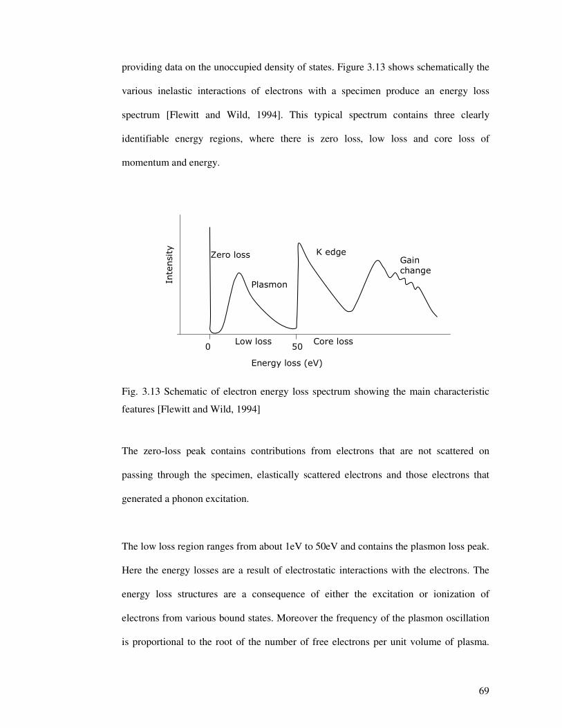
providing data on the unoccupied density of states. Figure 3.13 shows schematically the
various inelastic interactions of electrons with a specimen produce an energy loss
spectrum [Flewitt and Wild, 1994]. This typical spectrum contains three clearly
identifiable energy regions, where there is zero loss, low loss and core loss of
momentum and energy.
Core lossLow loss500
Energy loss (eV)
Intensity
K edgeGain change
Plasmon
Zero loss
Fig. 3.13 Schematic of electron energy loss spectrum showing the main characteristic
features [Flewitt and Wild, 1994]
The zero-loss peak contains contributions from electrons that are not scattered on
passing through the specimen, elastically scattered electrons and those electrons that
generated a phonon excitation.
The low loss region ranges from about 1eV to 50eV and contains the plasmon loss peak.
Here the energy losses are a result of electrostatic interactions with the electrons. The
energy loss structures are a consequence of either the excitation or ionization of
electrons from various bound states. Moreover the frequency of the plasmon oscillation
is proportional to the root of the number of free electrons per unit volume of plasma.

70
Thus the plasmon energy loss has the potential for providing an identification of a
material. According to the free electron theory, as the valence electron density changes
so does the energy of the plasmon loss peak.
The core loss (high loss) energy region extends from 50eV upwards. Here the energy
loss arises from the inelastic interactions with the inner atomic shells of the atoms
whereas the background intensity results from valence shell excitations. This produces
the characteristic edges used for elemental analysis. The most prominent spectral feature
in EELS is the inner shell edge profile (called high loss or inner shell spectra), and its
shape varies with the edge type (K, L, M, etc.), the electronic structure and the chemical
bonding.
EELS constitutes an indispensable tool for quantitative light element chemical analysis
with high spatial resolution. However, valuable additional chemical and structural
information may be obtained from the analysis of both the low-loss feature as well as
the electron energy-loss near edge structure (ELNES) associated with each high-energy
core-loss ionization edge [Schmid, 1995]. Since the Plasmon energy is a function of the
carrier charge density it may hold information on both the mass density (and thus the
structure and nature of chemical bonds) and valency state of the target material. ELNES
features essentially involve transitions of core electrons to unoccupied states just above
the Fermi level and thus may hold information on the density of final states, the
electronic structure, site symmetry and nearest neighbour coordination of the excited
atom in a given phase.

71
In the present application, the polishing debris were not only studied in TEM but also in
a STEM HB601, as shown in Fig. 3.14. It is a dedicated high resolution analytical
STEM, with a < 0.5 nm probe diameter. This makes it suitable for high spatial
resolution elemental analysis with EDX and EELS. STEM with its attached EDX and
EELS is used for characterization of polishing debris in terms of crystallography, phase
identification and sp2/sp
3 bonding character. By using the combination of EDX, EELS
and STEM, we cannot only observe the microstructure of the debris, but also can
simultaneously analyse the composition and chemical bonding information in a specific
region of interest.
Fig. 3.14 STEM instrument VGSTEM HB601
3.4 Temperature Measurement
Temperature can be measured via a diverse array of sensors, including thermocouples,
resistive temperature devices (RTDs and thermistors), infrared radiators, bimetallic
devices, liquid expansion devices, and change-of-state devices. All of them infer

72
temperature by sensing some change in a physical characteristic. The thermocouple
technique is the most widely used method of measuring temperatures in solid bodies
[Baker et al., 1953]. Thermocouple is a temperature sensor that consists of two
dissimilar materials in thermal contact [Dally et al., 1996]. They are cheap,
interchangeable, have standard connectors, easy to fabricate and install, and can
measure a wide range of temperatures. The disadvantage is the nonlinear output of the
thermocouple. However, in the present experiment, a data logger instrument (DT800
datataker) was used to record the output voltage and a personal computer with data
logger software was used to linearize the output and give readout in terms of
temperature directly. The other limitation is accuracy; system errors of less than 1°C
can be difficult to achieve. In the present work, the temperature will rise up to 500 °C or
greater, so the error is less than 0.2% which is negligible.
3.4.1 Principle of thermocouple
In 1822, an Estonian physician named Thomas Seebeck discovered that the junction
between two metals generates a voltage that is a function of temperature.
Thermocouples rely on this Seebeck effect [Pico(Technology), 2005, Tong, 2001].
Figure 3.15 shows the basic thermoelectric circuit [Kinzie, 1973]. A constant
thermoelectric current exists in the loop, provided that T1 and T2 are held at constant
unequal temperatures. The temperature difference between the two junctions is detected
by measuring the change in voltage (electromotive force, EMF) across the dissimilar
metals at the temperature measurement junction.

73
Fig. 3.15 The basic thermoelectric circuit
Figure 3.16 shows a practical circuit for measuring the thermoelectric voltage generated
by A and B, with junction temperatures at T1 and T2 [Kinzie, 1973]. T2 is the temperature
at the reference point; T1 is the temperature at the probe tip. Suppose that the Seebeck
coefficients of two dissimilar metallic materials A and B, and the wires C are SA, SB, and
SC respectively. The voltage output V is
dTTSTSdTTSdTTSdTTSdTTSV B
T
T
A
T
T
C
T
T
B
T
T
A
T
T
C )]()([)()()()(1
2
3
2
2
1
1
2
2
3
−=+++= ∫∫∫∫∫ (3.2)
If the Seebeck coefficient functions of the two thermocouple wire materials are pre-
calibrated and the reference temperature T2 is known (usually set by a 0°C ice bath), the
temperature at the probe tip becomes the only unknown and can be directly related to
the voltage readout.
Fig. 3.16 A practical circuit for thermocouple voltage measurement
T1 T2
B Current
A
T3
C
Reference T2
C A
B
Tip T1
V

74
In practice, vendors will provide calibration functions for their products. The high order
polynomials used for temperature determinations are of the form
T1-T2=a0+a1V+a2V2+…anV
n (3.3)
where a0, a1, a2, …, an are coefficients specified for each pair of thermocouple materials,
and T1-T2 is the difference in junction temperature in °C.
In the present experiment, the temperature could be read out directly from the PC based
data acquisition system by selecting the program in data logger software DeLogger, and
by entering the type of thermocouple and related parameters.
3.4.2 Thermocouple selection
When choosing a thermocouple, consideration should be given first to the thermocouple
type, and then to insulation and probe construction. All of these will have an effect on
the measurable temperature range, accuracy and reliability of the readings.
Common commercially available thermocouples are specified by ISA (Instrument
Society of America) types. Type E, J, K, T and N are base-metal thermocouples and
cover the majority of applications within industry over a range of –180 °C to +1300°C.
Type S, R, and B are noble-metal thermocouples and can be used up to about 2000°C.
Table 3.1 summarises the most popular types of thermocouple [2005, Tong, 2001].
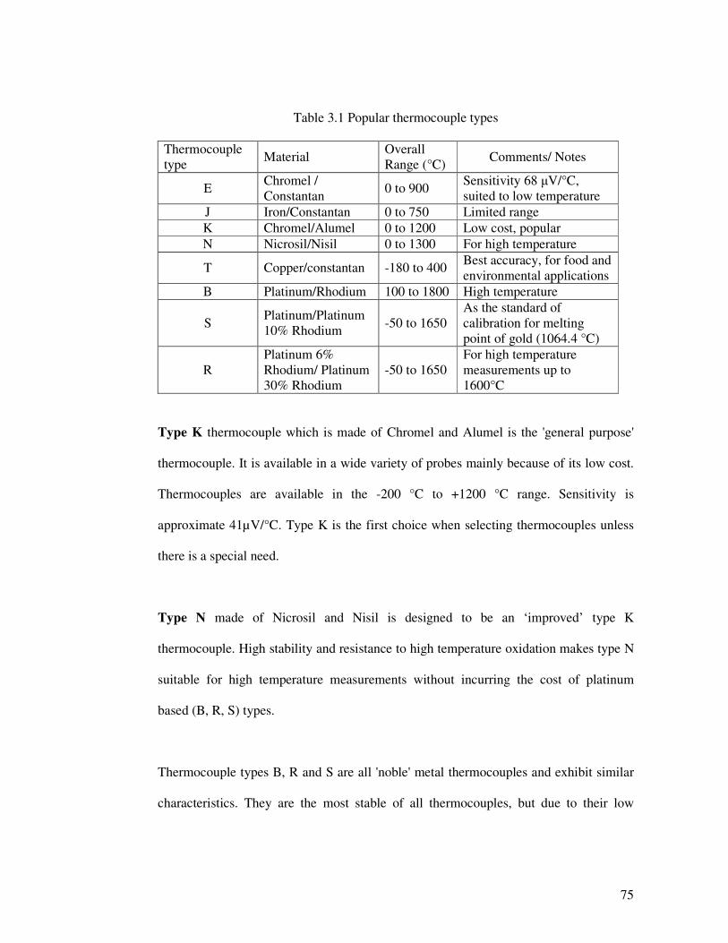
75
Table 3.1 Popular thermocouple types
Thermocouple type
Material Overall Range (°C)
Comments/ Notes
E Chromel / Constantan
0 to 900 Sensitivity 68 µV/°C, suited to low temperature
J Iron/Constantan 0 to 750 Limited range K Chromel/Alumel 0 to 1200 Low cost, popular N Nicrosil/Nisil 0 to 1300 For high temperature
T Copper/constantan -180 to 400 Best accuracy, for food and environmental applications
B Platinum/Rhodium 100 to 1800 High temperature
S Platinum/Platinum 10% Rhodium -50 to 1650
As the standard of calibration for melting point of gold (1064.4 °C)
R Platinum 6% Rhodium/ Platinum 30% Rhodium
-50 to 1650 For high temperature measurements up to 1600°C
Type K thermocouple which is made of Chromel and Alumel is the 'general purpose'
thermocouple. It is available in a wide variety of probes mainly because of its low cost.
Thermocouples are available in the -200 °C to +1200 °C range. Sensitivity is
approximate 41µV/°C. Type K is the first choice when selecting thermocouples unless
there is a special need.
Type N made of Nicrosil and Nisil is designed to be an ‘improved’ type K
thermocouple. High stability and resistance to high temperature oxidation makes type N
suitable for high temperature measurements without incurring the cost of platinum
based (B, R, S) types.
Thermocouple types B, R and S are all 'noble' metal thermocouples and exhibit similar
characteristics. They are the most stable of all thermocouples, but due to their low
76
sensitivity (approx 10 µV/°C) they are usually only used for high temperature
measurement (>300 °C).
In the present temperature measurement, the interface temperature is predicted to be the
melting point of stainless steel at 1420 °C, but a significant temperature drop can exist
at the measuring point which is approximately 0.5 mm from the interface. The measured
temperature would be significantly lower than the interface temperature. The
temperature rise due to the dissipation of frictional heat at the interface can be very high
but occurring in a very short distance [Kalin, 2004], because the real contact area is
much smaller than the nominal contact area [Guha and Roy Chowdhuri, 1996, Tian and
Kennedy, 1993]. In the present tests, as first trial, the most common Type K
thermocouple is selected due to its availability, low cost and ability to measure
temperatures up to 1200 °C. If Type K is insufficient, Type N and Type B are
considered to be suitable for the experiments.
3.4.3 Precautions and considerations for using thermocouples
In the present temperature measurement using thermocouples, it is necessary to be
aware of some factors to reduce the errors.
Firstly, it is important to make sure the measuring system is at the right place and the
thermocouple contacts well with the measuring point. When the thermocouple is
installed into the specimen, it is necessary to make sure the thermocouple is placed in
the right spot and can be insulated. Prior to the measurement of temperature (after the
installation), the system needs to be checked and calibrated by immersing the specimen
77
surface in a reference water to ensure the good contact of the thermocouple with the
measuring point.
Secondly, the effect of noise needs to be considered, since the on-line measurements are
carried out near the polishing motor, and the output from a thermocouple is a small
signal so it is prone to electrical noise pick up. Noise includes internal noise, which
would not greatly affect the high temperature level since the noise signal is relatively
small, and external noise. External noise is a factor because the signal leads act as
aerials picking up environmental electrical activity. To eliminate external noise, a
screened cable is used, and the signal wires are kept as short as possible by placing the
data logger close to the measuring point.
In addition, both thermocouple wires should be complete metal wires with no joins to
avoid unintentional junctions.
3.5 Summary
In this chapter, a number of characterization techniques were highlighted and their
application for the investigation of the PCD polishing process was discussed. Surface
topography of PCD specimens can be observed under optical, laser confocal, scanning
electron microscopy or by atomic force microscopy (AFM) at different resolutions.
Morphology and micro-structure of polishing debris can be obtained by using a
transmission electron microscope (TEM) or STEM. Surface roughness of PCD
specimens can be measured by a stylus roughness tester, a confocal microscope and/or
AFM. The combination of EDX, XRD, EELS and Raman spectrum analysis permits

78
detailed study of the chemical composition and structure, and atomic bonding
configuration of the PCD specimens and polishing debris. The polishing temperature
can be measured by a thermocouple with a computer-based data acquisition system. The
combination of the different methods will allow a comprehensive study of the PCD
polishing process, and will enable exploration of the mechanism of the process, and
drawing more accurate conclusions.