characteristics of silicon oxide thin films prepared by...
TRANSCRIPT
Available online at www.sciencedirect.com
www.elsevier.com/locate/cap
www.kps.or.kr
Current Applied Physics 9 (2009) 551–555
Characteristics of silicon oxide thin films prepared by solelectrophoretic deposition method using tetraethylorthosilicate
as the precursor
Sa-Kyun Rha a, Tammy P. Chou b, Guozhong Cao b, Youn-Seoung Lee c,*, Won-Jun Lee d
a Department of Materials Science and Engineering, Hanbat National University, Daejeon 305-719, Republic of Koreab Department of Materials Science and Engineering, University of Washington, Seattle, Washington, WA 98195, USA
c Department of Information Communication Engineering, Hanbat National University, Daejeon 305-719, Republic of Koread Department of Advanced Materials Engineering, Sejong University, Seoul 143-747, Republic of Korea
Received 21 September 2007; received in revised form 17 March 2008; accepted 25 March 2008Available online 15 May 2008
Abstract
Silicon dioxide films were prepared on p-type Si (100) substrates by sol electrophoretic deposition (EPD) using tetraethylorthosilicate(TEOS) at low temperature. According to the variation of sol dipping conditions, we estimated the characteristics of SiO2 films, such ascomposition, surface morphology, wet etch rate, breakdown voltage, etc. The growth rate of the film increased linearly with increasingTEOS quantity in solution. It increased exponentially with the increase in deposition time, and the film thickness was saturated atapproximately 200 nm on hydrophilic Si surface after more than 6 days. The growth rate of the EPD SiO2 films on the hydrophobicSi surface was much lower than that of the film on the hydrophilic Si surface.� 2008 Elsevier B.V. All rights reserved.
PACS: 68.55.jk
Keywords: Silica (SiO2); Electrophoretic deposition; Sol–gel; Tetraethylorthosilicate (TEOS); Flexible display
1. Introduction
The technological progression in thin film transistors(TFTs) has been opening up new possibilities in flat paneldisplays with electronic media. TFTs come in various typesand among them the research and development of high-speed and large-scale displays for use as television receiversis now proceeding at a vigorous pace. For the future, thereis much anticipation for large displays that provide greaterreality for object images; and portable, thin flexible dis-plays is also desirable that allow moving images to beenjoyed anytime and anywhere.
1567-1739/$ - see front matter � 2008 Elsevier B.V. All rights reserved.
doi:10.1016/j.cap.2008.03.023
* Corresponding author.E-mail address: [email protected] (Y.-S. Lee).
In recent years, the field of flexible displays is everexpanding with many new markets and technologies, andnew technologies are in demand for fabricating TFTs andother electronic devices on flexible substrates [1–5]. Thechallenge is to compose thin silicon and oxide films withoutdeforming or changing the properties of the polymer sub-strates. In case of the new generation poly-Si TFT usingglass substrate, a poly-Si layer with low resistance isformed in a device of top gate style. Therefore, the forma-tion of silicon films at considerably lower temperature hasbeen explored and developed by many researchers [6–10].However, there has been little research on oxide films asthe gate dielectric and inter metal dielectric of TFTs.
Sol–gel deposition of SiO2 films at lower processing tem-perature was also studied for the gate oxide of TFT forflexible displays. This sol–gel method has advantages such
552 S.-K. Rha et al. / Current Applied Physics 9 (2009) 551–555
as a growth of silicon oxide film at room temperature andcontrols of film thickness and capacitance through theadjustment of concentration. However, the poor qualityof the film deposited by sol–gel method with porous struc-ture has been a serious problem; not only integration indevice process may be very difficult due to the higher wetetch rate but also devices by this process are not well work-ing due to the poor electrical properties such as higher leak-age current and lower breakdown field.
One method with great potential for the oxide formationof flexible display TFTs and inter dielectric formationbetween metal to metal in semiconductor device is electro-phoretic deposition (EPD). In this method, an electric fieldis applied to a substrate, which is different to traditionalsol–gel deposition. Upon application of an external electricfield to a colloidal system or a sol, the constituent chargedparticles are set in motion in response to the electric field.EPD film shows higher density than that of film depositedby traditional sol–gel deposition methods. This is due tothe use of an oriented motion of charged particles to enrichthe solid particles from a colloidal dispersion or a sol ontothe surface of an electrode [11]. With these advantages,many researchers have been using the EPD method fornanowire and nanorod fabrication [12,13], and the applica-tion of the EPD method to SiO2 film is expected to improvethe capabilities of TFT for flexible displays.
In this study, silicon oxide thin films were deposited onp-type Si (100) substrates by sol EPD using tetraethylor-thosilicate (TEOS) in a chemical reactor with a biasing sys-tem. The deposition characteristics of the deposited filmswere estimated with varying TEOS quantity in solution,deposition time, and surface conditions. Physical and elec-trical properties of the deposited films were comparativelycharacterized with those of the silicon oxide films depositedby a sol dipping method.
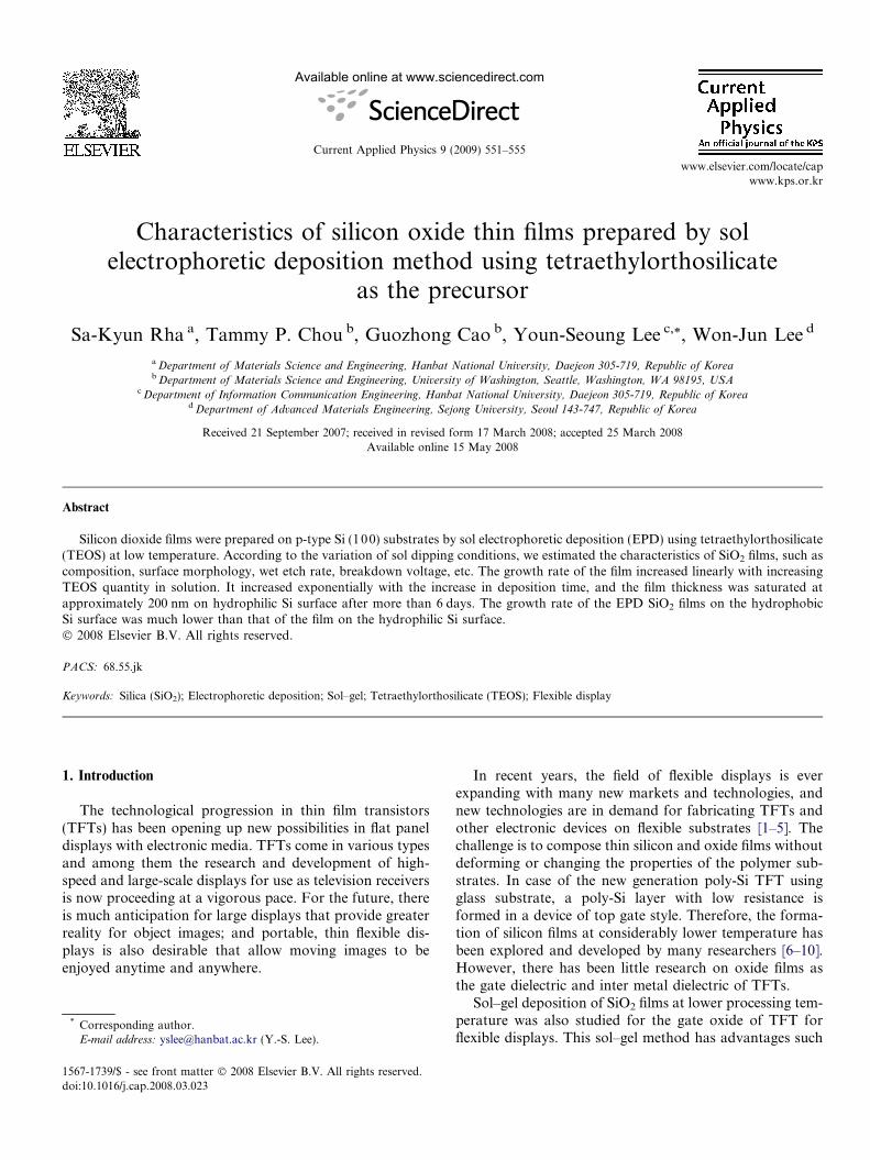
Fig. 1. The thickness and refractive index of sol–gel SiO2 films (Vbias = 0)as a function of the EtOH:TEOS volume ratio.
2. Experiments
Boron-doped Si (100) wafers were used as the substratesfor EPD of SiO2 film. Before film deposition, the surfacechemistry of the substrate was modified. Initially, the sub-strate surface is hydrophobic. In order to obtain a hydro-philic surface, the substrates were immersed in a dilutedhydrofluoric acid solution for 5 min to clean and removea native oxide layer previously formed by air exposure.The substrates were then rinsed with deionized water anddried by blown air.
Initial silica (SiO2) sol consisted of tetraethylorthosili-cate (TEOS), deionized water (DI-H2O), ethanol (EtOH),and hydrochloric acid (HCl). Hereafter, we will refer to thisinitial SiO2 sol as ‘TEOS’. In a 50 mL beaker containing astir bar, 3 mL of DI-H2O was added with 8 mL of EtOHand stirred at 500 RPM for �5 min at room temperature.To the above solution, 21 mL of TEOS and 0.09 mL ofHCl were added while stirring. The solution was thenallowed to stir at 500 RPM for �2 h at room temperature.
After stirring, unused portions of the sol were stored at�20 �C to prevent premature condensation and gelation.
The deposition of SiO2 film onto Si wafer was initiatedby the use of sol electrophoretic deposition (EPD). Beforedeposition, various amounts of EtOH was added to theTEOS solution to obtain diluted sols with an EtOH:TEOSvolume ratio of 2:1, 5:1, or 10:1. Additional amounts ofammonium hydroxide (NH4OH) were added to the varioussols to increase the pH above 2.2 at a pH value between 3and 4. A titanium (Ti) plate was used as the counter-elec-trode and the Si wafer substrate (working electrode) wasplaced �5 mm apart using an alumina spacer. The Si sub-strate size was 2 cm � 8 cm. The electrodes were immersedin 10 mL of sol and a potential of 1.2 V was applied to givean applied potential of 2.4 V/cm. After deposition, thefilms were dried at 100 �C for 1 h.
The thickness and the refractive index of the depositedfilms were measured using an ellipsometer (Sentech Co.SE400) in five points (top, center, bottom, left and rightin a sample), and the uniformity of sample-to-sample wasless than 5%. An atomic force microscope (AFM) systemwas used for measuring the surface. Wet etch rate of thedeposited films was evaluated using a diluted 500:1 DI-H2O:HF solution. To test the breakdown voltage of theoxide films, an aluminum electrode was formed by evapo-ration. The area of the electrode was 0.78 mm2, wherethe I–V data was measured with an HP 4140B system.
3. Result and discussion
The thickness and the refractive index of sol–gel depos-ited (without bias voltage) films were investigated as a func-tion of the TEOS quantity in solution using anEllipsometer. As shown in Fig. 1, the thickness and therefractive index of the sol–gel deposited films increased lin-early with increasing TEOS quantity. When the EtOH:TEOS volume ratio is 10:1, 5:1, and 2:1, the thickness ofthe deposited films were 94 nm, 75 nm, and 115 nm, respec-tively. It was thought that increasing the TEOS quantity in
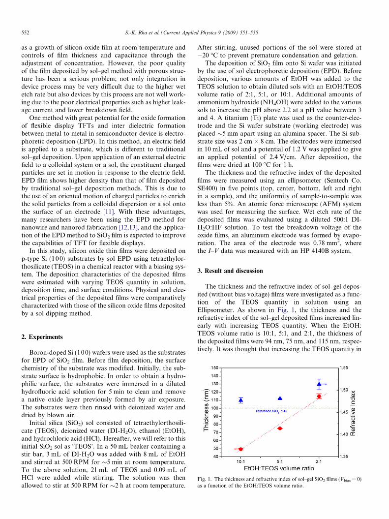
Fig. 2. The thickness of the sol–gel EPD SiO2 films (Vbias = 1.2 V) as afunction of the deposition time and the TEOS quantity.
Fig. 3. The refractive index of the sol–gel EPD SiO2 films (Vbias = 1.2 V)as a function of the deposition time and the TEOS quantity.
S.-K. Rha et al. / Current Applied Physics 9 (2009) 551–555 553
solution leads to an increase in the deposition rate. There-fore, an estimation in the deposition rate as a function ofthe variation of TEOS quantity in solution was made.
Fig. 2 shows the thickness of the deposited film as afunction of TEOS quantity and the deposition (=dipping)time by EPD using a bias voltage of 1.2 V. In general, asshown in Fig. 2, the thickness of the deposited filmsincreased with increasing TEOS quantity and dipping time.Specifically, with the variation of the dipping time before12 h, the thickness of the deposited films hardly changed.However, after 24 h, the thickness increased exponentiallywith increasing dipping time, and eventually becomes satu-rated when over 6 days (>144 h). The results showing nothickness change before 12 h could be due to the fact thatan incubation time is required in order to deposit SiO2 filmusing the EPD method. In addition, the saturation pointafter 6 days, where the film growth is stopped by an abruptdecrease in the deposition rate and where the thicknessdoes not change any further, could be due to a voltagedrop.
Furthermore, the thickness of the deposited SiO2 filmsby EPD in relation to the surface properties of the sub-strate (i.e. hydrophobic surfaces versus hydrophilic sur-faces), is also shown in Fig. 2. As shown, the SiO2 filmdoes not grow sufficiently on a hydrophobic surface, buteffectively grows on a hydrophilic surface. On the hydro-philic surface, film deposition is more likely to occurbecause the substrate surface is ‘‘water-like” with the pres-ence of surface –OH groups that help the attachment ofoxide particles to the substrate surface through the bond-age of –SiO groups (oxide particles) to the –OH groups(substrate surface). Therefore, it is assumed that the diffi-culty in the deposition of the SiO2 film on the hydrophobicsurface, as shown by the limited number of points in Fig. 2,is due to the less likely attachment of the oxide particles toa surface that is not ‘‘water-like.”
Fig. 3 shows the variation of the refractive index as afunction of deposition time and TEOS quantity. For allthe film samples, the refractive index approaches a stan-
dard value (1.46) of thermal oxide with increasing deposi-tion time. Specifically, for the film samples in which thevolume ratio of EtOH:TEOS is 2:1 and 5:1, the refractiveindex decreases linearly with increasing thickness of theoxide layer, as shown in Fig. 2. However, for the film sam-ples in which the volume ratio of EtOH:TEOS is 10:1, therefractive index decreases linearly with increasing thicknessof the oxide layer for the first 72 h, but then approaches thestandard value of 1.46 after 72 h. From these results, it isassumed that the decrease in the refractive index is due tothe formation of a porous film by an abrupt increase inthe film thickness of the oxide layer.
According to the variation of the volume ratio ofEtOH:TEOS, the surface morphology in the film samplesformed by EPD and sol–gel methods was measured byAFM, as shown in Fig. 4. Before heat treatment, the sur-face morphology of all the film samples by sol–gel deposi-tion in which the EtOH:TEOS volume ratio is 10:1, 5:1,and 2:1 is rough, as shown in Fig. 4a, d, and g, respectively.In addition, the number and the size of the pores in the filmsample in Fig. 4a formed using a sol with EtOH:TEOS vol-ume ratio of 10:1 are larger and smaller, respectively, thanthat in the film sample in Fig. 4g formed using a sol withEtOH:TEOS volume ratio of 2:1. After heat treatmentfor 1 hour at 100 �C for these film samples, the pores areclearly shown in Figs. 4b, e, and h; and the trend is similarto the results before heat treatment, as shown in Fig. 4a, d,and g, respectively. However, after heat treatment for thefilm samples by the EPD method, as shown in Fig. 4c, f,and i, the pores nearly disappear.
The wet etch rates of the films were estimated with adiluted 1000:1 DIH2O:HF solution to investigate the den-sity and the integrity of the films. Fig. 5 shows the resultsof the etch rate in annealed film samples prepared by elec-trophoretic deposition and sol–gel methods. The etch ratein the films prepared by the EPD method decreased byabout 50–60% in comparison with that of the films madeby typical sol–gel methods. From these results, it is
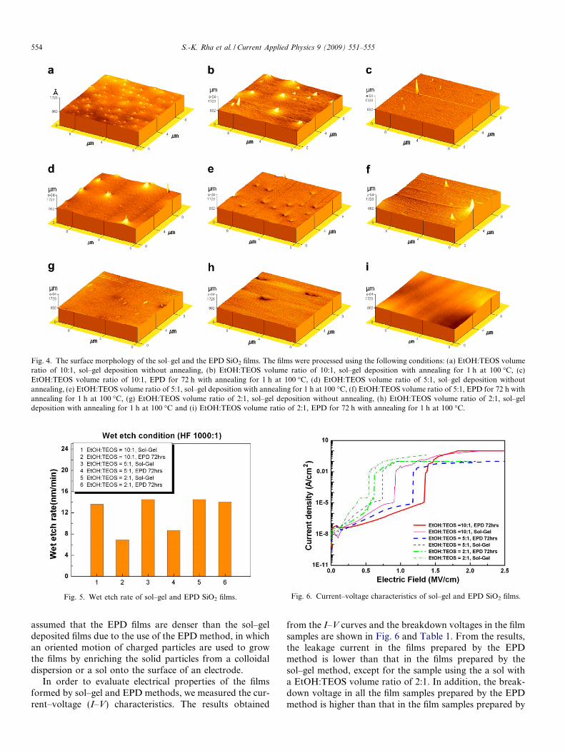
Fig. 4. The surface morphology of the sol–gel and the EPD SiO2 films. The films were processed using the following conditions: (a) EtOH:TEOS volumeratio of 10:1, sol–gel deposition without annealing, (b) EtOH:TEOS volume ratio of 10:1, sol–gel deposition with annealing for 1 h at 100 �C, (c)EtOH:TEOS volume ratio of 10:1, EPD for 72 h with annealing for 1 h at 100 �C, (d) EtOH:TEOS volume ratio of 5:1, sol–gel deposition withoutannealing, (e) EtOH:TEOS volume ratio of 5:1, sol–gel deposition with annealing for 1 h at 100 �C, (f) EtOH:TEOS volume ratio of 5:1, EPD for 72 h withannealing for 1 h at 100 �C, (g) EtOH:TEOS volume ratio of 2:1, sol–gel deposition without annealing, (h) EtOH:TEOS volume ratio of 2:1, sol–geldeposition with annealing for 1 h at 100 �C and (i) EtOH:TEOS volume ratio of 2:1, EPD for 72 h with annealing for 1 h at 100 �C.
Fig. 5. Wet etch rate of sol–gel and EPD SiO2 films. Fig. 6. Current–voltage characteristics of sol–gel and EPD SiO2 films.
554 S.-K. Rha et al. / Current Applied Physics 9 (2009) 551–555
assumed that the EPD films are denser than the sol–geldeposited films due to the use of the EPD method, in whichan oriented motion of charged particles are used to growthe films by enriching the solid particles from a colloidaldispersion or a sol onto the surface of an electrode.
In order to evaluate electrical properties of the filmsformed by sol–gel and EPD methods, we measured the cur-rent–voltage (I–V) characteristics. The results obtained
from the I–V curves and the breakdown voltages in the filmsamples are shown in Fig. 6 and Table 1. From the results,the leakage current in the films prepared by the EPDmethod is lower than that in the films prepared by thesol–gel method, except for the sample using the a sol witha EtOH:TEOS volume ratio of 2:1. In addition, the break-down voltage in all the film samples prepared by the EPDmethod is higher than that in the film samples prepared by
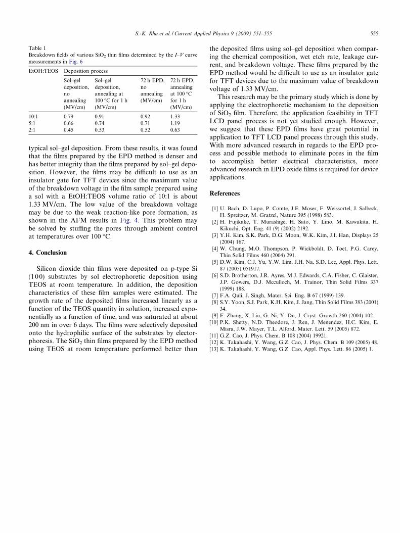
Table 1Breakdown fields of various SiO2 thin films determined by the I–V curvemeasurements in Fig. 6
EtOH:TEOS Deposition process
Sol–geldeposition,noannealing(MV/cm)
Sol–geldeposition,annealing at100 �C for 1 h(MV/cm)
72 h EPD,noannealing(MV/cm)
72 h EPD,annealingat 100 �Cfor 1 h(MV/cm)
10:1 0.79 0.91 0.92 1.335:1 0.66 0.74 0.71 1.192:1 0.45 0.53 0.52 0.63
S.-K. Rha et al. / Current Applied Physics 9 (2009) 551–555 555
typical sol–gel deposition. From these results, it was foundthat the films prepared by the EPD method is denser andhas better integrity than the films prepared by sol–gel depo-sition. However, the films may be difficult to use as aninsulator gate for TFT devices since the maximum valueof the breakdown voltage in the film sample prepared usinga sol with a EtOH:TEOS volume ratio of 10:1 is about1.33 MV/cm. The low value of the breakdown voltagemay be due to the weak reaction-like pore formation, asshown in the AFM results in Fig. 4. This problem maybe solved by stuffing the pores through ambient controlat temperatures over 100 �C.
4. Conclusion
Silicon dioxide thin films were deposited on p-type Si(100) substrates by sol electrophoretic deposition usingTEOS at room temperature. In addition, the depositioncharacteristics of these film samples were estimated. Thegrowth rate of the deposited films increased linearly as afunction of the TEOS quantity in solution, increased expo-nentially as a function of time, and was saturated at about200 nm in over 6 days. The films were selectively depositedonto the hydrophilic surface of the substrates by elector-phoresis. The SiO2 thin films prepared by the EPD methodusing TEOS at room temperature performed better than
the deposited films using sol–gel deposition when compar-ing the chemical composition, wet etch rate, leakage cur-rent, and breakdown voltage. These films prepared by theEPD method would be difficult to use as an insulator gatefor TFT devices due to the maximum value of breakdownvoltage of 1.33 MV/cm.
This research may be the primary study which is done byapplying the electrophoretic mechanism to the depositionof SiO2 film. Therefore, the application feasibility in TFTLCD panel process is not yet studied enough. However,we suggest that these EPD films have great potential inapplication to TFT LCD panel process through this study.With more advanced research in regards to the EPD pro-cess and possible methods to eliminate pores in the filmto accomplish better electrical characteristics, moreadvanced research in EPD oxide films is required for deviceapplications.
References
[1] U. Bach, D. Lupo, P. Comte, J.E. Moser, F. Weissortel, J. Salbeck,H. Spreitzer, M. Gratzel, Nature 395 (1998) 583.
[2] H. Fujikake, T. Murashige, H. Sato, Y. Lino, M. Kawakita, H.Kikuchi, Opt. Eng. 41 (9) (2002) 2192.
[3] Y.H. Kim, S.K. Park, D.G. Moon, W.K. Kim, J.I. Han, Displays 25(2004) 167.
[4] W. Chung, M.O. Thompson, P. Wickboldt, D. Toet, P.G. Carey,Thin Solid Films 460 (2004) 291.
[5] D.W. Kim, C.J. Yu, Y.W. Lim, J.H. Na, S.D. Lee, Appl. Phys. Lett.87 (2005) 051917.
[6] S.D. Brotherton, J.R. Ayres, M.J. Edwards, C.A. Fisher, C. Glaister,J.P. Gowers, D.J. Mcculloch, M. Trainor, Thin Solid Films 337(1999) 188.
[7] F.A. Quli, J. Singh, Mater. Sci. Eng. B 67 (1999) 139.[8] S.Y. Yoon, S.J. Park, K.H. Kim, J. Jang, Thin Solid Films 383 (2001)
34.[9] F. Zhang, X. Liu, G. Ni, Y. Du, J. Cryst. Growth 260 (2004) 102.
[10] P.K. Shetty, N.D. Theodore, J. Ren, J. Menendez, H.C. Kim, E.Misra, J.W. Mayer, T.L. Alford, Mater. Lett. 59 (2005) 872.
[11] G.Z. Cao, J. Phys. Chem. B 108 (2004) 19921.[12] K. Takahashi, Y. Wang, G.Z. Cao, J. Phys. Chem. B 109 (2005) 48.[13] K. Takahashi, Y. Wang, G.Z. Cao, Appl. Phys. Lett. 86 (2005) 1.