ald of lanthanide oxide thin films
TRANSCRIPT
5/13/2018 ALD of Lanthanide Oxide Thin Films - slidepdf.com
http://slidepdf.com/reader/full/ald-of-lanthanide-oxide-thin-films 1/69
Helsinki University of Technology
Inorganic Chemistry Publication Series
Espoo 2006 No. 6
ATOMIC LAYER DEPOSITION OF LANTHANI DE OXIDE
THIN FILMS
Jani Päiväsaari
Dissertation for the degree of Doctor of Science in Technology to be presented with due
permission of the Department of Chemical Technology for public examination and debate in
Auditorium V1 at Helsinki University of Technology (Espoo, Finland) on the 19th
of May, 2006,
at 12 noon.
Helsinki University of Technology
Department of Chemical Technology
Laboratory of I norganic and Analytical Chemistr y
Teknillinen korkeakoulu
Kemian tekniikan osasto
Epäorgaanisen ja analyyttisen kemian laboratorio
5/13/2018 ALD of Lanthanide Oxide Thin Films - slidepdf.com
http://slidepdf.com/reader/full/ald-of-lanthanide-oxide-thin-films 2/69
Distribution:
Helsinki University of Technology
Laboratory of I norganic and Analytical Chemistry
P.O. Box 6100
FIN-02150 TKK, FINLAND
© Jani Päiväsaari
ISBN 951-22-8163-5
ISSN 1458-5154
Otamedia Oy
Espoo 2006
5/13/2018 ALD of Lanthanide Oxide Thin Films - slidepdf.com
http://slidepdf.com/reader/full/ald-of-lanthanide-oxide-thin-films 3/69
ABSTRACT
This thesis describes the processing of thin films of lanthanide (Ln) oxides by atomic
layer deposition (ALD) technique. Deposition of all binary lanthanide oxides was
studied, excluding terbium oxide and the unstable promethium oxide. In addition,gadolinium oxide-doped cerium dioxide films were grown by combining the
respective binary processes developed in this work. Films were characterized by a
wide range of analytical techniques for structural, compositional, electrical, and
surface properties. As background for the study, some promising application areas
for lanthanide and rare earth (RE) oxide thin films are briefly introduced, and the
ALD technique is explained. Reported ALD processes for RE oxides are then
reviewed.
Ln(thd)3 and ozone were successfully utilized for deposition of most members of the
Ln2O3 series. The deposited films were nearly stoichiometric Ln2O3 with only low
concentrations of carbon, hydrogen, and fluorine impurities. Films were also uniform
and smooth. Relative permittivity values were in the range of 8.4−11.1.
In addition to Er(thd)3, Er2O3 films were also grown with (CpMe)3Er andEr(tBu2amd)3 as metal precursors. All processes resulted in pure and nearly
stoichiometric Er2O3 films. The growth rate of 1.5 Å/cycle obtained with the
(CpMe)3Er/H2O process was approximately four and six times the rates measured for
erbia films grown by the Er(tBu2amd)3 /O3 and Er(thd)3 /O3 processes, respectively.
Cerium dioxide films were successfully deposited with use of Ce(thd)4 or
Ce(thd)3(phen) and ozone as precursors. Gadolinium oxide-doped CeO2 (CGO) filmswere then grown by combining the Ln(thd)x /O3 processes for the respective binary
oxides. ALD-grown CGO films were dense and conformal, but the Ce:Gd ratio in the
films could not be optimized to the level required in solid oxide fuel cells.
5/13/2018 ALD of Lanthanide Oxide Thin Films - slidepdf.com
http://slidepdf.com/reader/full/ald-of-lanthanide-oxide-thin-films 4/69
PREFACE
This work was carried out in the Laboratory of Inorganic and Analytical Chemistry,
Helsinki University of Technology, between January 2000 and September 2005.
I would like to thank my supervisor Professor Lauri Niinistö for the opportunity to
work in his ALD group and for his kind and expert help whenever needed. I am most
grateful to my instructor Dr. Matti Putkonen for fruitful research ideas and advice, as
well as to the members of the ALD group and especially my co-authors Mr. Jaakko
Niinistö, Dr. Charles Dezelah, and Lic.Sci. (Tech.) Anne Kosola for their many
contributions. I wish to thank Dr. Minna Nieminen for all the help in finalizing this
thesis. I am indebted to the personnel at the Laboratory for practical help.
Special thanks are owed to Dr. Kaupo Kukli for carrying out the electrical
measurements and XRR analyses and providing invaluable help in interpreting the
results, to Drs. Timo Sajavaara and Kai Arstila for performing the TOF-ERD
analyses, to Professors Markku Leskelä (Laboratory of Inorganic Chemistry) and
Juhani Keinonen (Accelerator Laboratory) at the University of Helsinki for providing
the necessary facilities for these measurements, and to Professor Charles Winter(Wayne State University, Detroit) and Dr. Emmanuel Gourba (Ecole Nationale
Supérieure de Chimie de Paris) for fruitful collaboration in the fields of precursor
chemistry and solid oxide fuel cells, respectively.
Warmest thanks belong to my beloved wife Minna. Thank you for your unfailing
encouragement and support over these many years.
This work was supported by the Foundation of Technology (TES), the Wihuri
Foundation, and the Gustav Komppa Fund of the Kordelin Foundation.
Espoo, February 2006
Jani Päiväsaari
5/13/2018 ALD of Lanthanide Oxide Thin Films - slidepdf.com
http://slidepdf.com/reader/full/ald-of-lanthanide-oxide-thin-films 5/69
LIST OF PUBLICATIONS
The thesis is based on the following publications, which are referred to in the text by
Roman numerals I-VII:
I Päiväsaari, J., Putkonen, M., and Niinistö, L., A comparative study onlanthanide oxide thin films grown by atomic layer deposition, Thin Solid
Films 472 (2005) 275-281.
II Kosola, A., Päiväsaari, J., Putkonen, M., and Niinistö, L., Neodymium oxide
and neodymium aluminate thin films by atomic layer deposition, Thin Solid
Films 479 (2005) 152-159.
III Päiväsaari, J., Putkonen, M., Sajavaara, T., and Niinistö, L., Atomic layer
deposition of rare earth oxides: erbium oxide films from β-diketonate and
ozone precursors, J. Alloys Compd. 374 (2004) 124-128.
IV Päiväsaari, J., Niinistö, J., Arstila, K., Kukli, K., Putkonen, M., and Niinistö,
L., High growth rate of erbium oxide thin films in atomic layer deposition
from (CpMe)3Er and water precursors, Chem. Vap. Deposition 11 (2005)
415-419.
V Päiväsaari, J., Dezelah, C.L., Back, D., El-Kaderi, H.M., Heeg, M.J.,Putkonen, M., Niinistö, L., and Winter, C.H., Synthesis, structure, and
properties of volatile lanthanide complexes containing amidinate ligands:
application for Er2O3 film growth by atomic layer deposition, J. Mater.
Chem. 15 (2005) 4224-4233.
VI Päiväsaari, J., Putkonen, M., and Niinistö, L., Cerium dioxide buffer layers at
low temperature by atomic layer epitaxy, J. Mater. Chem. 12 (2002) 1828-
1832.
VII Gourba, E., Ringuedé, A., Cassir, M., Päiväsaari, J., Niinistö, J., Putkonen,
M., and Niinistö, L., Microstructural and electrical properties of gadolinium
doped ceria thin films prepared by atomic layer deposition (ALD),
Electrochem. Soc. Proc. 2003-7 (2003) 267-274.
5/13/2018 ALD of Lanthanide Oxide Thin Films - slidepdf.com
http://slidepdf.com/reader/full/ald-of-lanthanide-oxide-thin-films 6/69
THE AUTHOR’S CONTRIBUTION
Publications I and III The author defined the research plan for the experimental
work and performed all practical work except TOF-ERDAand AFM, interpreted the results, and wrote the
manuscript.
Publications II The author participated in the planning of the research,
performed some of the experiments, and participated in
interpreting the results and writing the manuscript.
Publication IV The author had a major role in defining the research plan
and carried out all practical work, except TOF-ERDA,
AFM, and characterization of the electrical properties. The
author interpreted the results and wrote a major part of the
manuscript.
Publication V The author defined the research plan for the ALD section
of the manuscript, carried out the depositions, and did all
thin film analyses except TOF-ERDA and AFM. The
author contributed to the writing of the ALD section of the
manuscript.
Publication VI The author defined the research plan with the co-authors
and performed all practical work except TOF-ERDA and
AFM. The author interpreted the results and wrote the
manuscript together with the co-authors.
Publication VII The author defined the research plan for the ALD part of
the manuscript and carried out the depositions and some of
the thin film analyses. The author contributed to the
writing of the ALD part of the manuscript.
5/13/2018 ALD of Lanthanide Oxide Thin Films - slidepdf.com
http://slidepdf.com/reader/full/ald-of-lanthanide-oxide-thin-films 7/69
LIST OF ABBREVIATIONS AND ACRONYMS
acac Acetyl acetonate, 2,4-pentanedionate
AFM Atomic force microscopy
ALCVD Atomic layer chemical vapor depositionALD Atomic layer deposition
ALE Atomic layer epitaxy
ALP Atomic layer processing
amd Amidinate
bipy Bipyridine
CGO Gadolinia-doped ceria, Ce1-xGdxO2-0.5x
Cp Cyclopentadienyl
CVD Chemical vapor deposition
dmae Dimethylaminoethoxide
DTA Differential thermal analysis
EBE Electron beam evaporation
EDS Energy dispersive x-ray spectroscopy
EOT Equivalent oxide thickness
fdh 1,1,1-Trifluoro-5,5-dimethyl-2,4-hexanedionate
FTIR Fourier transform infrared spectroscopy
IR Infrared spectroscopy
IT-SOFC Intermediate temperature solid oxide fuel cell
Ln Lanthanide element (Ce-Lu)
LSM Lanthanum strontium manganate, La1-xSrxMnO3
mmp 1-Methoxy-2-methyl-2-propanolate
MOSFET Metal-oxide-semiconductor field effect transistor
Phen 1,10-Phenanthroline
RE Rare earth (Y, Sc, La, Ce-Lu)
REALD Radical-enhanced atomic layer deposition
rms Root mean square
SEM Scanning electron microscopy
SOFC Solid oxide fuel cell
tetea Triethoxy-triethyleneamine
tetraglyme Tetraethyleneglycol-dimethylether
5/13/2018 ALD of Lanthanide Oxide Thin Films - slidepdf.com
http://slidepdf.com/reader/full/ald-of-lanthanide-oxide-thin-films 8/69
thd 2,2,6,6-Tetramethyl-3,5-heptanedionate
TG Thermogravimetry
TOF-ERDA Time-of-flight elastic recoil detection analysis
tod 2,2,6,6-Tetramethyl-3,5-octanedionate
TMA Trimethylaluminum, (CH3)3AlXRD X-ray diffraction
XRR X-ray reflectometry
YSZ Yttria-stabilized zirconia, Y2O3-ZrO2
5/13/2018 ALD of Lanthanide Oxide Thin Films - slidepdf.com
http://slidepdf.com/reader/full/ald-of-lanthanide-oxide-thin-films 9/69
CONTENTS
ABSTRACT............................................................................................................ 3
PREFACE ............................................................................................................... 4
LIST OF PUBLICATIONS .................................................................................... 5THE AUTHOR’S CONTRIBUTION..................................................................... 6
LIST OF ABBREVIATIONS AND ACRONYMS................................................ 7
CONTENTS............................................................................................................ 9
1. INTRODUCTION ........................................................................................ 10
2. POTENTIAL APPLICATIONS FOR RARE EARTH OXIDE FILMS ...... 12
2.1. Metal-oxide-semiconductor field effect transistors .............................. 12
2.2. Optical waveguides............................................................................... 14
2.3. Solid oxide fuel cells............................................................................. 16
3. ATOMIC LAYER DEPOSITION OF RARE EARTH OXIDES ................ 18
3.1. Principle of atomic layer deposition ..................................................... 18
3.2. Literature review on ALD of rare earth oxide thin films ...................... 21
3.2.1. ALD of binary RE oxides ............................................................. 21
3.2.2. ALD of multi-component RE-containing oxides.......................... 29
4. EXPERIMENTAL........................................................................................ 34
4.1. Precursors and substrates ...................................................................... 34
4.2. Deposition of lanthanide oxide thin films............................................. 35
4.2.1. Ln(thd)3 /O3 process for Ln2O3 films ............................................. 37
4.2.2. Processes for Er2O3 films .............................................................. 38
4.2.3. ALD of CeO2, Ce1-xGdxO2-0.5x, and PrOx films............................. 38
4.3. Film characterization............................................................................. 39
5. RESULTS AND DISCUSSION ................................................................... 41
5.1. Ln2O3 thin films from Ln(thd)3 and O3 ................................................. 41
5.2. Er2O3 thin films from different processes............................................. 48
5.3. CeO2 and Ce1-xGdxO2-0.5x thin films...................................................... 52
5.4. PrOx thin films ...................................................................................... 55
6. CONCLUSIONS........................................................................................... 57
REFERENCES...................................................................................................... 59
5/13/2018 ALD of Lanthanide Oxide Thin Films - slidepdf.com
http://slidepdf.com/reader/full/ald-of-lanthanide-oxide-thin-films 10/6910
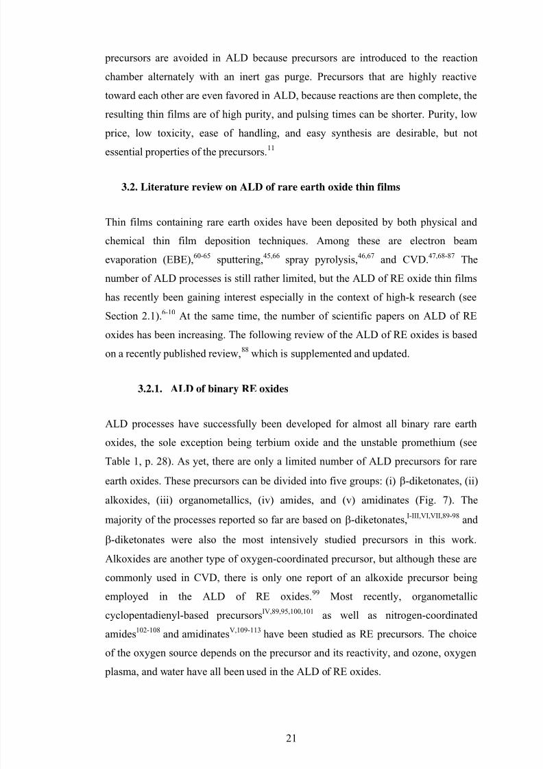
1. INTRODUCTION
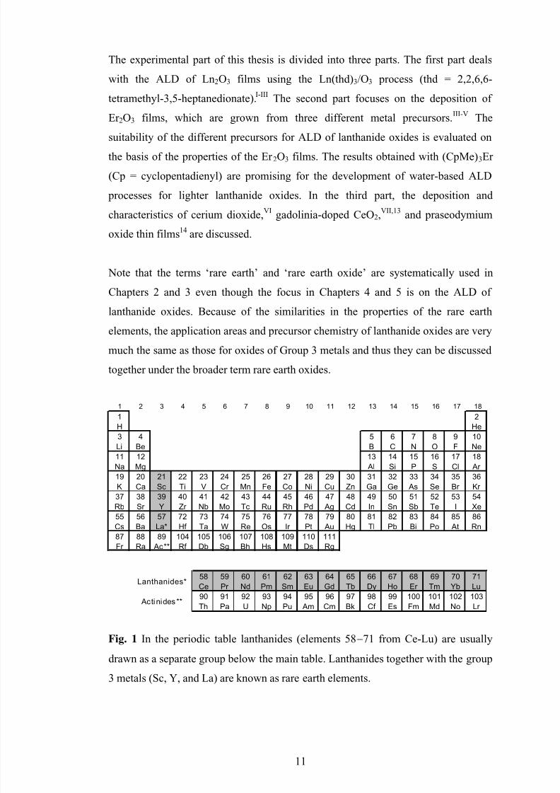
The rare earth elements consist of Group 3 metals (21Sc, 39Y, and 57La) and
lanthanides (58Ce→71Lu). The rare earths (RE) and particularly the lanthanides (Ln)
form, chemically and physically, a more or less homogeneous group, the largest inthe periodic table (Fig. 1). This is a consequence of the lanthanide contraction, which
refers to the gradual decrease in the ionic radius of the elements from lanthanum to
lutetium by 17%. Owing to the lanthanide contraction, trivalent yttrium is near in
size to the heavier lanthanides and the chemical behaviour is closely similar.1 Many
physical and chemical properties of the rare earth oxides vary only slightly from
element to element.2,3
The use of rare earths is extensive. Examples of their classical and most recent
applications include automotive catalytic converters, glass polishing, petroleum
refining catalysts, phosphors, and permanent magnets.4 RE oxide thin films have
already been utilized or they are being considered as potential materials in a variety
of applications, particularly in optics and electronics. Some application areas where
atomic layer deposited (ALD) RE oxide thin films may find use are presented in
Chapter 2. By virtue of their high relative permittivity values (k=12.3−14.8),5 RE
oxides have been considered as candidates for new gate dielectrics in
microelectronics.6-10 Er2O3 is being used as a doping material in amplifying optical
waveguides, while RE2O3-doped CeO2 films could be employed as oxide ion
conducting electrolytes in solid oxide fuel cells (SOFC). The components discussed
in Chapter 2 were not actually prepared during this work, but rather ALD processes
for many of the relevant materials were designed.
The primary aim of the present work was to develop ALD processes for lanthanide
oxides, most of which had not earlier been deposited by ALD technique. ALD can be
utilized to produce very thin, but yet dense, uniform, and conformal films.11,12 As
background to the study, the general principle of ALD is described in Section 3.1,
and a short literature review on previously reported ALD processes for RE oxides is
presented in Section 3.2
5/13/2018 ALD of Lanthanide Oxide Thin Films - slidepdf.com
http://slidepdf.com/reader/full/ald-of-lanthanide-oxide-thin-films 11/6911
The experimental part of this thesis is divided into three parts. The first part deals
with the ALD of Ln2O3 films using the Ln(thd)3 /O3 process (thd = 2,2,6,6-
tetramethyl-3,5-heptanedionate).I-III The second part focuses on the deposition of
Er2O3 films, which are grown from three different metal precursors.III-V The
suitability of the different precursors for ALD of lanthanide oxides is evaluated onthe basis of the properties of the Er2O3 films. The results obtained with (CpMe)3Er
(Cp = cyclopentadienyl) are promising for the development of water-based ALD
processes for lighter lanthanide oxides. In the third part, the deposition and
characteristics of cerium dioxide,VI gadolinia-doped CeO2,VII,13 and praseodymium
oxide thin films14 are discussed.
Note that the terms ‘rare earth’ and ‘rare earth oxide’ are systematically used inChapters 2 and 3 even though the focus in Chapters 4 and 5 is on the ALD of
lanthanide oxides. Because of the similarities in the properties of the rare earth
elements, the application areas and precursor chemistry of lanthanide oxides are very
much the same as those for oxides of Group 3 metals and thus they can be discussed
together under the broader term rare earth oxides.
Fig. 1 In the periodic table lanthanides (elements 58−71 from Ce-Lu) are usually
drawn as a separate group below the main table. Lanthanides together with the group
3 metals (Sc, Y, and La) are known as rare earth elements.
1 2 3 4 5 6 7 8 9 10 11 12 13 14 15 16 17 18
1H
2He
3
Li
4
Be
5
B
6
C
7
N
8
O
9
F
10
Ne
11
Na
12
Mg
13
Al
14
Si
15
P
16
S
17
Cl
18
Ar
19
K
20
Ca
21
Sc
22
Ti
23
V
24
Cr
25
Mn
26
Fe
27
Co
28
Ni
29
Cu
30
Zn
31
Ga
32
Ge
33
As
34
Se
35
Br
36
Kr
37
Rb
38
Sr
39
Y
40
Zr
41
Nb
42
Mo
43
Tc
44
Ru
45
Rh
46
Pd
47
Ag
48
Cd
49
In
50
Sn
51
Sb
52
Te
53
I
54
Xe
55
Cs
56
Ba
57
La*
72
Hf
73
Ta
74
W
75
Re
76
Os
77
Ir
78
Pt
79
Au
80
Hg
81
Tl
82
Pb
83
Bi
84
Po
85
At
86
Rn
87
Fr
88
Ra
89
Ac**
104
Rf
105
Db
106
Sg
107
Bh
108
Hs
109
Mt
110
Ds
111
Rg
Lanthanides*58
Ce
59
Pr
60
Nd
61
Pm
62
Sm
63
Eu
64
Gd
65
Tb
66
Dy
67
Ho
68
Er
69
Tm
70
Yb
71
Lu
Actinides**90
Th
91
Pa
92
U
93
Np
94
Pu
95
Am
96
Cm
97
Bk
98
Cf
99
Es
100
Fm
101
Md
102
No
103
Lr
5/13/2018 ALD of Lanthanide Oxide Thin Films - slidepdf.com
http://slidepdf.com/reader/full/ald-of-lanthanide-oxide-thin-films 12/6912
2. POTENTIAL APPLICATIONS FOR RARE EARTH OXIDE FILMS
This chapter discusses three promising application areas for rare earth oxide thin
films and indicates the suitability of the ALD technique to the processing of these
films. ALD processes for many of the relevant materials will be introduced inChapters 3 and 4.
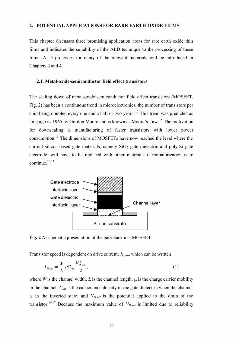
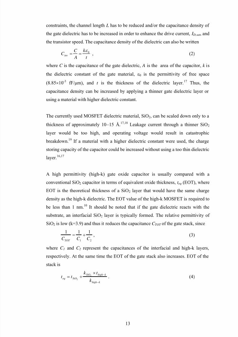
2.1. Metal-oxide-semiconductor field effect transistors
The scaling down of metal-oxide-semiconductor field effect transistors (MOSFET,
Fig. 2) has been a continuous trend in microelectronics, the number of transistors per
chip being doubled every one and a half or two years.10 This trend was predicted as
long ago as 1965 by Gordon Moore and is known as Moore’s Law.15 The motivation
for downscaling is manufacturing of faster transistors with lower power
consumption.16 The dimensions of MOSFETs have now reached the level where the
current silicon-based gate materials, namely SiO2 gate dielectric and poly-Si gate
electrode, will have to be replaced with other materials if miniaturization is to
continue.10,17
Fig. 2 A schematic presentation of the gate stack in a MOSFET.
Transistor speed is dependent on drive current, I D,sat , which can be written
2
2,
,sat D
invsat D
V C
L
W I µ = , (1)
where W is the channel width, L is the channel length, µ is the charge carrier mobility
in the channel, C inv is the capacitance density of the gate dielectric when the channel
is in the inverted state, and V D,sat is the potential applied to the drain of thetransistor.16,17 Because the maximum value of V D,sat is limited due to reliability
Gate electrode
Interfacial layer
Gate dielectric
Interfacial layer Channel layer
Silicon substrate
5/13/2018 ALD of Lanthanide Oxide Thin Films - slidepdf.com
http://slidepdf.com/reader/full/ald-of-lanthanide-oxide-thin-films 13/6913
constraints, the channel length L has to be reduced and/or the capacitance density of
the gate dielectric has to be increased in order to enhance the drive current, I D,sat , and
the transistor speed. The capacitance density of the dielectric can also be written
t
k
A
C C inv
0ε == , (2)
where C is the capacitance of the gate dielectric, A is the area of the capacitor, k is
the dielectric constant of the gate material, ε0 is the permittivity of free space
(8.85×10⁻³ fF/ µm), and t is the thickness of the dielectric layer.17 Thus, the
capacitance density can be increased by applying a thinner gate dielectric layer or
using a material with higher dielectric constant.
The currently used MOSFET dielectric material, SiO2, can be scaled down only to athickness of approximately 10−15 Å.17,18 Leakage current through a thinner SiO2
layer would be too high, and operating voltage would result in catastrophic
breakdown.19 If a material with a higher dielectric constant were used, the charge
storing capacity of the capacitor could be increased without using a too thin dielectric
layer.16,17
A high permittivity (high-k) gate oxide capacitor is usually compared with aconventional SiO2 capacitor in terms of equivalent oxide thickness, t eq (EOT), where
EOT is the theoretical thickness of a SiO2 layer that would have the same charge
density as the high-k dielectric. The EOT value of the high-k MOSFET is required to
be less than 1 nm.10 It should be noted that if the gate dielectric reacts with the
substrate, an interfacial SiO2 layer is typically formed. The relative permittivity of
SiO2 is low (k=3.9) and thus it reduces the capacitance C TOT of the gate stack, since
21
111C C C TOT
+= , (3)
where C 1 and C 2 represent the capacitances of the interfacial and high-k layers,
respectively. At the same time the EOT of the gate stack also increases. EOT of the
stack is
k high
k highSiO
SiOeqk
t k t t
−
−×+= 2
2. (4)
5/13/2018 ALD of Lanthanide Oxide Thin Films - slidepdf.com
http://slidepdf.com/reader/full/ald-of-lanthanide-oxide-thin-films 14/6914
At the moment, it appears that the next generation of gate dielectrics will be based on
hafnium oxides and silicates, but in the rather near future these Hf-based materials
may have to be replaced as well.10 Rare earth oxides are among the candidates for the
next generation of gate dielectrics. They are thermodynamically stable in contact
with silicon,20
and their relative permittivity values are large enough, being in therange of 12.3−14.8 for bulk oxides5 but a value as high as 27 has been reported for a
La2O3 thin film.21 The band gap and conduction band offset values of RE oxides also
meet the requirements for gate dielectrics, being ca. 4−6 eV and >2 eV,
respectively.8-10,22 There are many other critical factors influencing the choice of the
next gate dielectric material. In the case of RE oxides, issues such as interface
quality, morphology, compatibility with other gate materials, film processing
compatibility, and reliability call for further research.10,17
The scaling down of MOSFETs places demands on the thin film deposition technique as well, and ALD
may well be the method-of-choice for the deposition of gate dielectrics in the near
future10,22,23 since it can be utilized to deposit very thin and yet conformal films even
into deep trenches.11,12
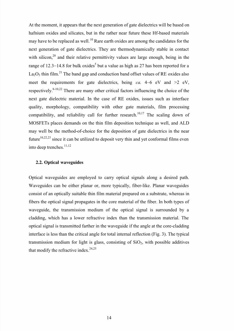
2.2. Optical waveguides
Optical waveguides are employed to carry optical signals along a desired path.
Waveguides can be either planar or, more typically, fiber-like. Planar waveguides
consist of an optically suitable thin film material prepared on a substrate, whereas in
fibers the optical signal propagates in the core material of the fiber. In both types of
waveguide, the transmission medium of the optical signal is surrounded by a
cladding, which has a lower refractive index than the transmission material. The
optical signal is transmitted farther in the waveguide if the angle at the core-cladding
interface is less than the critical angle for total internal reflection (Fig. 3). The typical
transmission medium for light is glass, consisting of SiO2, with possible additives
that modify the refractive index.24,25
5/13/2018 ALD of Lanthanide Oxide Thin Films - slidepdf.com
http://slidepdf.com/reader/full/ald-of-lanthanide-oxide-thin-films 15/6915
Fig. 3 Light is guided along the transmission medium by total internal reflection.θ is
the incidence angle of light at the core-cladding interface.
The intensity of the optical signal is reduced along the waveguide due to absorption
and scattering.24,25 The transmission loss in SiO2-containing fibers is lowest at
approximately 1.50 µm, which is therefore used as a standard wavelength in opticaltelecommunication systems.24-26 The attenuation (or transmission loss) of the optical
signal has to be compensated by employing optical amplifiers. In most cases, the
amplifying materials contain rare earth ions as dopants, and erbium-doped materials
are of great interest.26 The transition energy between the first excited state and the
ground state of Er3+ ions corresponds to a wavelength of 1.53 µm. Therefore, if Er3+
ions are excited externally, for example by a laser, the transition energy can be
employed to provide gain in the optical signal. Use of ytterbium ions as sensitizers inEr-doped amplifiers enables the use of shorter wavelength lasers.26 Solubility of rare
earth ions in pure silica is very low, however, and clusters of RE ions will quickly
start to form reducing the number of optically active RE ions.27 However, if silica is
first doped with Al2O3 the clustering is eliminated and doping concentrations for RE
ions can be much higher.27 In planar waveguides, the transmission medium can be
simply aluminum oxide doped with RE ions.26,28,29 The concentration of Er3+ ions has
to be carefully controlled in order to achieve optimum amplification. In planar Er-doped Al2O3 waveguides the optimal Er concentration is approximately 3×10²⁰
ions/cm3 (∼0.3 at.-%).26,28
With ALD the level of doping can be controlled in a straightforward manner, even on
large deposition areas, and ALD should therefore be a highly suitable method for
preparing planar waveguides for integrated optical circuits. In fact, Solehmainen et
al.29
have already demonstrated the fabrication of planar Er-doped alumina
waveguides by ALD, but their process needs further development to achieve a more
5/13/2018 ALD of Lanthanide Oxide Thin Films - slidepdf.com
http://slidepdf.com/reader/full/ald-of-lanthanide-oxide-thin-films 16/6916
homogeneous distribution of Er-atoms. From the above, it is clear that the
development of new ALD processes for Er2O3 and other rare earth oxides is of
considerable importance.
2.3. Solid oxide fuel cells
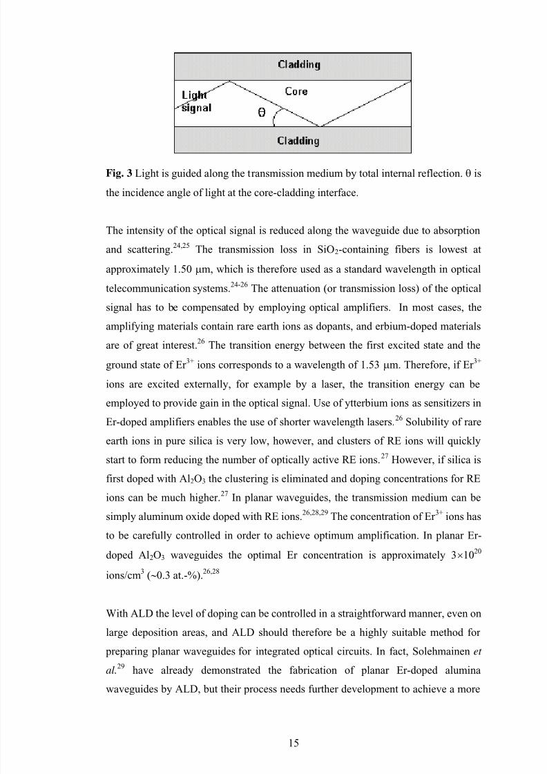
Fuel cells convert the chemical energy of fuels such as H2, CO, hydrocarbons, and
alcohols to electrical energy. The operating principle of solid oxide fuel cells (SOFC,
Fig. 4) is the following: (1) The fuel reacts at the anode with oxide ions that have
travelled through the solid electrolyte, and (2) the liberated electrons travel through
an external circuit to the cathode, where (3) oxygen is catalytically reduced to oxide
ions.
Fig. 4 Schematic presentation of a typical SOFC comprising (La,Sr)MnO3 and Ni-
YSZ electrodes and YSZ electrolyte.
The most commonly employed electrolyte material today is yttria-stabilized zirconia
(YSZ), while (La,Sr)MnO3 (LSM) and Ni-YSZ cermet have been used as electrodes.
The operating temperature of state-of-the-art SOFCs having the Ni-YSZ/YSZ/LSM
structure is above 950 °C. Lowering of the operating temperature to 500−750 °C
would lengthen the lifetime of SOFCs and allow the use of less expensive
interconnecting materials. However, there are many thermally activated processes in
SOFCs, such as oxide ion conductivity, chemical reactions at electrodes, and internal
reforming of fuel, and adjustment of the operating temperature requires a careful
balancing of the benefits and disadvantages.30 Intermediate temperature SOFCs (IT-
(La,Sr)MnO3
YSZ
Ni-YSZ cermet
Electrolyte
Cathode
Anode
5/13/2018 ALD of Lanthanide Oxide Thin Films - slidepdf.com
http://slidepdf.com/reader/full/ald-of-lanthanide-oxide-thin-films 17/6917
SOFC) operated at 500−750 °C can be realized if the decrease in the ionic
conductivity of the electrolyte is compensated by selecting a more conductive
electrolyte material or using a thinner electrolyte layer.30
Potential new electrolyte materials for IT-SOFCs include CeO2,31-34 ZrO2,35 ThO236 and Bi2O3,
37 typically doped with rare earth oxides. RE2O3-CeO2 solid solutions with
fluorite structure are a well-known group of oxide ion conductors31,38 and are
considered as the most promising alternative materials for IT-SOFCs despite their
instability under reducing atmospheres.31,39 Special attention has been paid to
gadolinia-doped ceria (CGO) or Ce1-xGdxO2-0.5x, which appears to have the highest
conductivity among ceria-based electrolytes.31,33 As the dopant concentration in the
CGO system is increased, the conductivity passes through a maximum.40
Themaximum in ionic conductivity is obtained when ca. 10 at.-% of Ce is substituted by
Gd, i.e. Ce0.9Gd0.1O1.95, but the exact position of the maximum is also dependent on
the temperature.40 Other interesting ceria-based systems are samaria-doped and
yttria-doped ceria, which exhibit about the same conducting properties as the CGO
electrolyte.31,41,42
The thickness of the electrolyte layer in thin film IT-SOFCs is typically 5−10 µm,which is very much less than the 200 µm used in conventional SOFC devices. This
means that even less conductive electrolyte materials, such as YSZ, can be employed
in thin film IT-SOFCs.43 The processing of the electrolyte and the electrodes by thin
film deposition techniques also improves properties of the interface.44 Although YSZ
thin film electrolytes have been the prime research target, ceria-based thin film
electrolytes and interlayers have been widely studied as well. Ceria-based interlayers
between the actual electrolyte and the electrodes have been reported to enhance the
cell performance because they significantly reduce polarization losses.45 Previously,
CGO electrolyte films have been processed by e.g. spray pyrolysis,46 aerosol-assisted
metal-organic CVD,47 and tape casting.48 Furthermore, screen-printing49 and
sputtering45 methods have been utilized to deposit CGO and yttria-doped CeO2
interlayers, respectively. In this work, ALD was applied for the preparation of CGO
thin film electrolytes.VII,13
5/13/2018 ALD of Lanthanide Oxide Thin Films - slidepdf.com
http://slidepdf.com/reader/full/ald-of-lanthanide-oxide-thin-films 18/6918
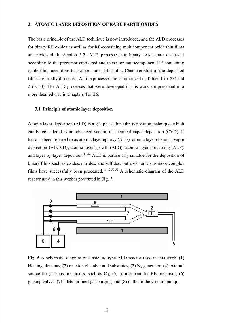
3. ATOMIC LAYER DEPOSITION OF RARE EARTH OXIDES
The basic principle of the ALD technique is now introduced, and the ALD processes
for binary RE oxides as well as for RE-containing multicomponent oxide thin films
are reviewed. In Section 3.2, ALD processes for binary oxides are discussedaccording to the precursor employed and those for multicomponent RE-containing
oxide films according to the structure of the film. Characteristics of the deposited
films are briefly discussed. All the processes are summarized in Tables 1 (p. 28) and
2 (p. 33). The ALD processes that were developed in this work are presented in a
more detailed way in Chapters 4 and 5.
3.1. Principle of atomic layer deposition
Atomic layer deposition (ALD) is a gas-phase thin film deposition technique, which
can be considered as an advanced version of chemical vapor deposition (CVD). It
has also been referred to as atomic layer epitaxy (ALE), atomic layer chemical vapor
deposition (ALCVD), atomic layer growth (ALG), atomic layer processing (ALP),
and layer-by-layer deposition.11,12 ALD is particularly suitable for the deposition of
binary films such as oxides, nitrides, and sulfides, but also numerous more complex
films have successfully been processed.11,12,50-52 A schematic diagram of the ALD
reactor used in this work is presented in Fig. 5.
Fig. 5 A schematic diagram of a satellite-type ALD reactor used in this work. (1)
Heating elements, (2) reaction chamber and substrates, (3) N2 generator, (4) external
source for gaseous precursors, such as O3, (5) source boat for RE precursor, (6)
pulsing valves, (7) inlets for inert gas purging, and (8) outlet to the vacuum pump.
5/13/2018 ALD of Lanthanide Oxide Thin Films - slidepdf.com
http://slidepdf.com/reader/full/ald-of-lanthanide-oxide-thin-films 19/6919
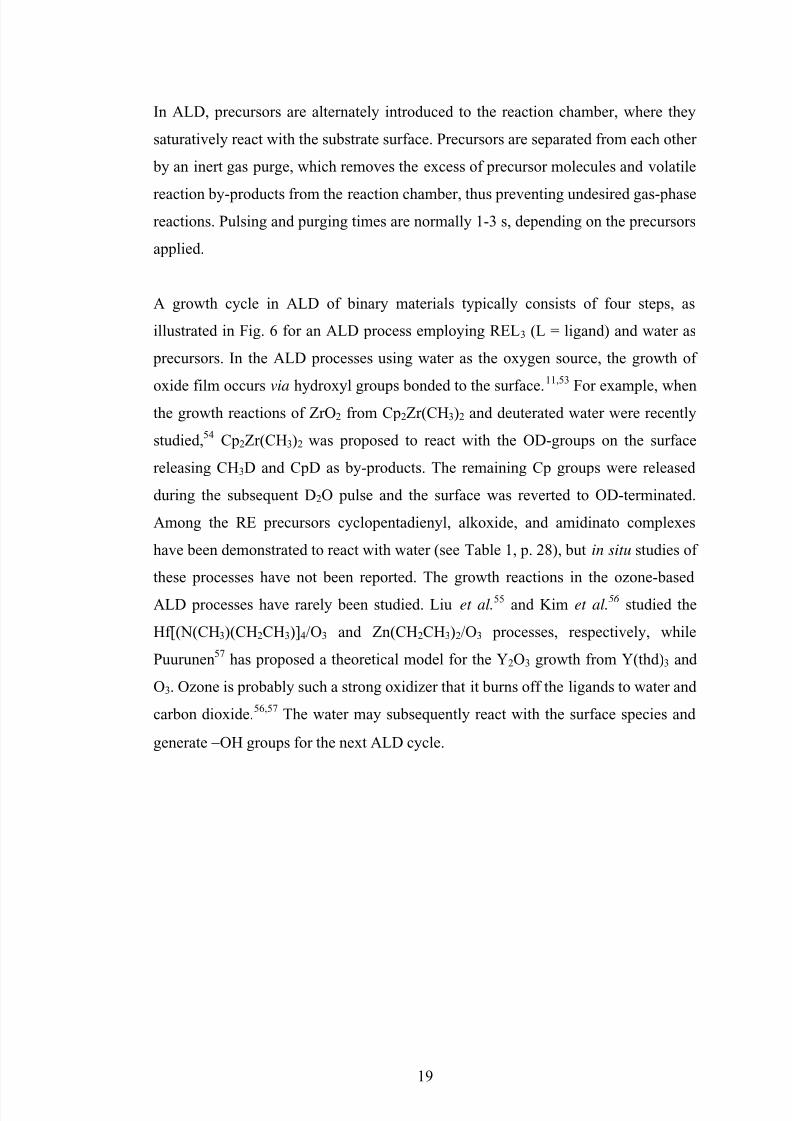
In ALD, precursors are alternately introduced to the reaction chamber, where they
saturatively react with the substrate surface. Precursors are separated from each other
by an inert gas purge, which removes the excess of precursor molecules and volatile
reaction by-products from the reaction chamber, thus preventing undesired gas-phasereactions. Pulsing and purging times are normally 1-3 s, depending on the precursors
applied.
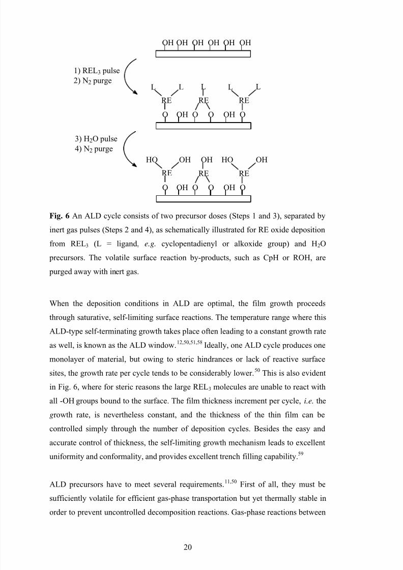
A growth cycle in ALD of binary materials typically consists of four steps, as
illustrated in Fig. 6 for an ALD process employing REL3 (L = ligand) and water as
precursors. In the ALD processes using water as the oxygen source, the growth of
oxide film occurs via hydroxyl groups bonded to the surface.
11,53
For example, whenthe growth reactions of ZrO2 from Cp2Zr(CH3)2 and deuterated water were recently
studied,54 Cp2Zr(CH3)2 was proposed to react with the OD-groups on the surface
releasing CH3D and CpD as by-products. The remaining Cp groups were released
during the subsequent D2O pulse and the surface was reverted to OD-terminated.
Among the RE precursors cyclopentadienyl, alkoxide, and amidinato complexes
have been demonstrated to react with water (see Table 1, p. 28), but in situ studies of
these processes have not been reported. The growth reactions in the ozone-based
ALD processes have rarely been studied. Liu et al.55
and Kim et al.56
studied the
Hf[(N(CH3)(CH2CH3)]4 /O3 and Zn(CH2CH3)2 /O3 processes, respectively, while
Puurunen57 has proposed a theoretical model for the Y2O3 growth from Y(thd)3 and
O3. Ozone is probably such a strong oxidizer that it burns off the ligands to water and
carbon dioxide.56,57 The water may subsequently react with the surface species and
generate −OH groups for the next ALD cycle.
5/13/2018 ALD of Lanthanide Oxide Thin Films - slidepdf.com
http://slidepdf.com/reader/full/ald-of-lanthanide-oxide-thin-films 20/6920
OH OH OH OH OH OH
L L
REOOHOOOHO
RE
L
RE
LL
1) REL3 pulse2) N2 purge
3) H2O pulse4) N2 purge
HO OH
RE
OH
RE
O OH O O OH O
RE
OHHO
Fig. 6 An ALD cycle consists of two precursor doses (Steps 1 and 3), separated by
inert gas pulses (Steps 2 and 4), as schematically illustrated for RE oxide deposition
from REL3 (L = ligand, e.g. cyclopentadienyl or alkoxide group) and H2O
precursors. The volatile surface reaction by-products, such as CpH or ROH, are
purged away with inert gas.
When the deposition conditions in ALD are optimal, the film growth proceeds
through saturative, self-limiting surface reactions. The temperature range where this
ALD-type self-terminating growth takes place often leading to a constant growth rate
as well, is known as the ALD window.12,50,51,58 Ideally, one ALD cycle produces one
monolayer of material, but owing to steric hindrances or lack of reactive surface
sites, the growth rate per cycle tends to be considerably lower.50 This is also evident
in Fig. 6, where for steric reasons the large REL3 molecules are unable to react with
all -OH groups bound to the surface. The film thickness increment per cycle, i.e. the
growth rate, is nevertheless constant, and the thickness of the thin film can be
controlled simply through the number of deposition cycles. Besides the easy and
accurate control of thickness, the self-limiting growth mechanism leads to excellent
uniformity and conformality, and provides excellent trench filling capability.59
ALD precursors have to meet several requirements.11,50 First of all, they must be
sufficiently volatile for efficient gas-phase transportation but yet thermally stable inorder to prevent uncontrolled decomposition reactions. Gas-phase reactions between
5/13/2018 ALD of Lanthanide Oxide Thin Films - slidepdf.com
http://slidepdf.com/reader/full/ald-of-lanthanide-oxide-thin-films 21/6921
precursors are avoided in ALD because precursors are introduced to the reaction
chamber alternately with an inert gas purge. Precursors that are highly reactive
toward each other are even favored in ALD, because reactions are then complete, the
resulting thin films are of high purity, and pulsing times can be shorter. Purity, low
price, low toxicity, ease of handling, and easy synthesis are desirable, but notessential properties of the precursors.11
3.2. Literature review on ALD of rare earth oxide thin films
Thin films containing rare earth oxides have been deposited by both physical and
chemical thin film deposition techniques. Among these are electron beam
evaporation (EBE),60-65 sputtering,45,66 spray pyrolysis,46,67 and CVD.47,68-87 The
number of ALD processes is still rather limited, but the ALD of RE oxide thin films
has recently been gaining interest especially in the context of high-k research (see
Section 2.1).6-10 At the same time, the number of scientific papers on ALD of RE
oxides has been increasing. The following review of the ALD of RE oxides is based
on a recently published review,88 which is supplemented and updated.
3.2.1. ALD of binary RE oxides
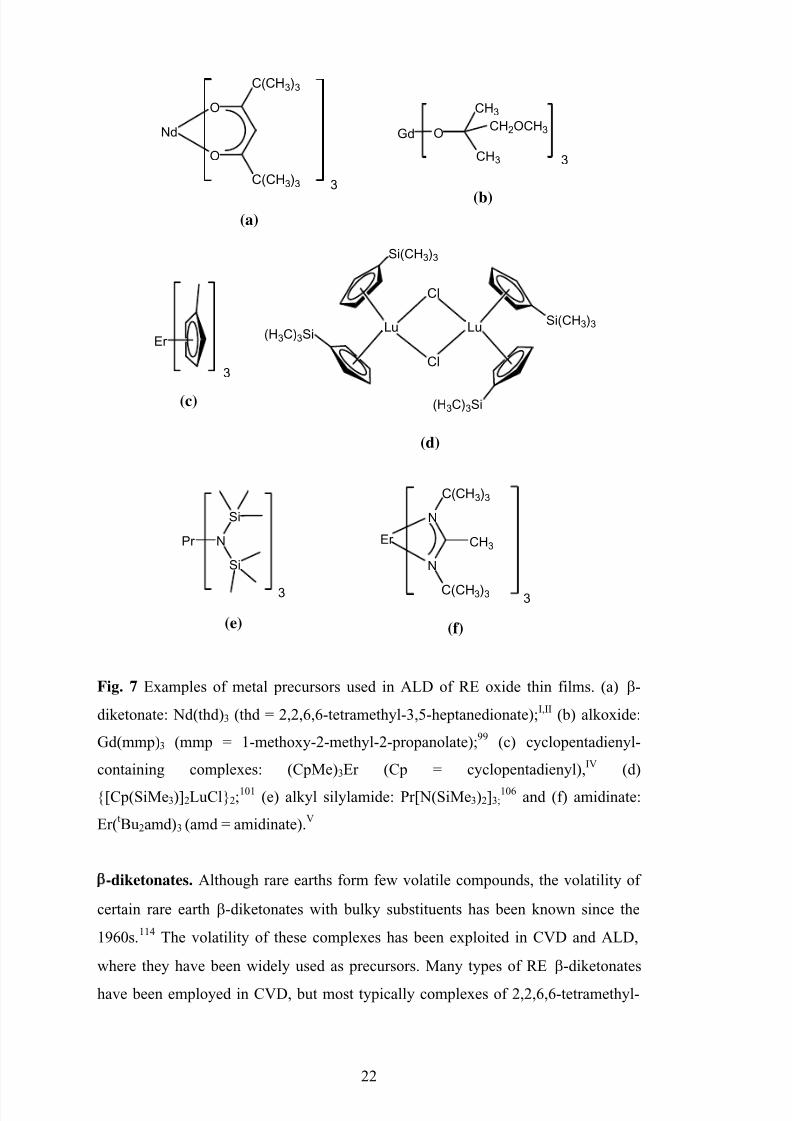
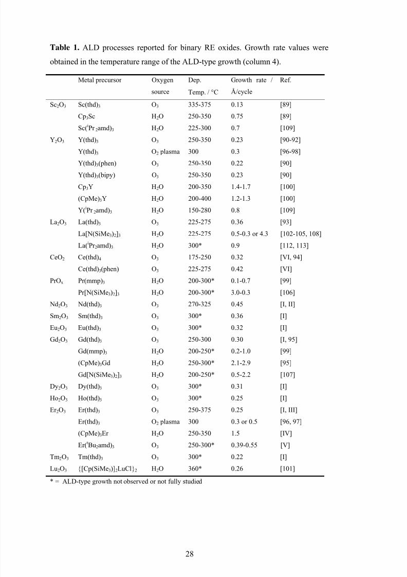
ALD processes have successfully been developed for almost all binary rare earth
oxides, the sole exception being terbium oxide and the unstable promethium (see
Table 1, p. 28). As yet, there are only a limited number of ALD precursors for rare
earth oxides. These precursors can be divided into five groups: (i) β-diketonates, (ii)
alkoxides, (iii) organometallics, (iv) amides, and (v) amidinates (Fig. 7). The
majority of the processes reported so far are based on β-diketonates,I-III,VI,VII,89-98 and
β-diketonates were also the most intensively studied precursors in this work.Alkoxides are another type of oxygen-coordinated precursor, but although these are
commonly used in CVD, there is only one report of an alkoxide precursor being
employed in the ALD of RE oxides.99 Most recently, organometallic
cyclopentadienyl-based precursorsIV,89,95,100,101 as well as nitrogen-coordinated
amides102-108 and amidinatesV,109-113 have been studied as RE precursors. The choice
of the oxygen source depends on the precursor and its reactivity, and ozone, oxygen
plasma, and water have all been used in the ALD of RE oxides.
5/13/2018 ALD of Lanthanide Oxide Thin Films - slidepdf.com
http://slidepdf.com/reader/full/ald-of-lanthanide-oxide-thin-films 22/6922
C(CH3)3
C(CH3)3
O
O
Nd
3
N
N
CH3
C(CH3)3
C(CH3)3
Er
3
Er
3
Pr
O
3
N
Si
Si
3
(a)
(e) (f)
(c)
CH3
CH3
CH2OCH3Gd
(b)
Lu Lu
Cl
Cl
(H3C)3Si
Si(CH3)3
(H3C)3SiSi(CH3)3
(d)
Fig. 7 Examples of metal precursors used in ALD of RE oxide thin films. (a) β-
diketonate: Nd(thd)3 (thd = 2,2,6,6-tetramethyl-3,5-heptanedionate);I,II (b) alkoxide:
Gd(mmp)3 (mmp = 1-methoxy-2-methyl-2-propanolate);99 (c) cyclopentadienyl-
containing complexes: (CpMe)3Er (Cp = cyclopentadienyl),IV (d)
{[Cp(SiMe3)]2LuCl}2;101 (e) alkyl silylamide: Pr[N(SiMe3)2]3;
106 and (f) amidinate:
Er(tBu2amd)3 (amd = amidinate).V
β-diketonates. Although rare earths form few volatile compounds, the volatility of
certain rare earth β-diketonates with bulky substituents has been known since the
1960s.114 The volatility of these complexes has been exploited in CVD and ALD,
where they have been widely used as precursors. Many types of RE β-diketonates
have been employed in CVD, but most typically complexes of 2,2,6,6-tetramethyl-
5/13/2018 ALD of Lanthanide Oxide Thin Films - slidepdf.com
http://slidepdf.com/reader/full/ald-of-lanthanide-oxide-thin-films 23/6923
3,5-heptanedione, H(thd). In fact, all RE oxides have been deposited from RE(thd)x
precursors by conventional CVD,68-75 plasma-enhanced CVD (PECVD),76 or liquid
injection CVD.77,78 Even bulkier ligands such as 2,2,6,6-tetramethyl-3,5-
octanedione, H(tod) have occasionally been used.72 Fluorination of ligands enhances
the volatility,114,115
and fluorinated complexes like Ce(fdh)4 (fdh = 1,1,1-trifluoro-5,5-dimethyl-2,4-hexanedionate) have been exploited as well.69 In addition, different
adducts of RE β-diketonate complexes have been applied, including La(thd)3(tetea),79
Ce(thd)3(phen),69 Gd(thd)3(tetraglyme),80 and Ln(acac)3(phen)81,82 (tetea = triethoxy-
triethyleneamine; phen = 1,10-phenanthroline; tetraglyme = tetraethyleneglycol-
dimethylether; acac = acetylacetonate).
Among the many volatile β-diketonates, only thd-based complexes have beenutilized as precursors in ALD. These are also the most frequently used rare earth
source in ALD.I-III,VI,VII,89-98 The major part of the RE(thd)x-based ALD processes
were developed in the course of the present work and are discussed in a more
detailed way in Chapters 4 and 5. All thd-based processes have certain general
features, however, which are appropriately mentioned here. RE(thd)x complexes are
volatile, thermally stable solids,116-118 which are easy to synthesize.119 They are also
easy to handle and store, being relatively stable in contact with air. The optimizeddeposition temperature range (ALD window) is wide, typically extending from about
250 to 350 °C. β-Diketonate-based processes also have some drawbacks. First, thd-
complexes do not react with water but require a stronger oxidizer such as ozone. This
could be a problem in the high-k applications. Secondly, the growth rates obtained in
RE(thd)x /O3 processes are rather low, typically on the order of 0.2−0.45 Å/cycle.
Neutral N-donor adducts of Y(thd)3 and Ce(thd)3 complexes have been used asprecursors in ALD of Y2O3 and CeO2.
VI,90 Comparison of Y(thd)3 /O3,
Y(thd)3(phen)/O3, and Y(thd)3(bipy)/O3 (bipy = bipyridine) processes and of
Ce(thd)4 /O3 and Ce(thd)3(phen)/O3 processes failed to reveal any distinct advantages
of adducts in the deposition of oxide films. The growth rate, the deposition
temperature range, and impurity levels of carbon and hydrogen were similar for
adduct and non-adduct precursors in both cases. Moreover, Y2O3 films deposited
from Y(thd)3(phen) and Y(thd)3(bipy) were observed to contain a small amount
(0.1−0.3 at.-%) of nitrogen.90 Adducts such as Ce(thd)3(phen) may nevertheless be
5/13/2018 ALD of Lanthanide Oxide Thin Films - slidepdf.com
http://slidepdf.com/reader/full/ald-of-lanthanide-oxide-thin-films 24/6924
useful when trivalent cerium ions are needed (e.g. in ALD of electroluminescent
SrS:Ce thin films) because adducts help to coordinatively saturate the Ce3+ ion,
thereby stabilizing the otherwise unstable oxidation state of cerium.120
Thd precursors have also been used in radical-enhanced ALD (REALD), but so farthe results have not been promising. In this technique, reactive oxygen radicals from
oxygen plasma are reacted with Er(thd)3 or Y(thd)3 to deposit the respective oxide
thin films.96-98 In the case of both Er2O3 and Y2O3 films, the ALD window was at
200−300 °C. The obtained growth rate was 0.3−0.5 Å/cycle depending on the
precursor pulsing times,96-98 but the carbon impurity level was high being
approximately 26 at.-%. Furthermore, the pulse times needed in the REALD process
for Er2O3 were ∼5−10 min or hundreds of times longer than in a typical flow-typeALD reactor. The reason for such long pulsing times was not discussed in these
reports, but they are related to the reactor design. The REALD reactor had a larger
reaction chamber, which was equipped with in situ instruments, and it was operated
under ultra high vacuum conditions.96-98
Alkoxides. In general, alkoxides are widely used in CVD,121 but only recently has
the CVD of rare earth oxides from alkoxide precursors been reported.
83-87
Theproblem has been the tendency of the simple RE alkoxides to form oligomers, which
are of low volatility.121 Recently LaOx, PrOx, Nd2O3, and GdOx were grown by liquid
injection CVD with Ln(mmp)3 (mmp = 1-methoxy-2-methyl-2-propanolate) alkoxide
complex as the metal precursor.83-87 The same precursors have also been applied in a
modified ALD technique, called liquid injection ALD, for the processing of PrOx and
Gd2O3 films.99 In this technique, the precursor solution is injected into a vaporizer
and further directed into the reactor chamber, while oxidizer, such as water vapor, is
directly pulsed into the reactor chamber. Between the precursor pulses the chamber is
purged with inert gas. In ALD of PrOx and Gd2O3 films,99 the alkoxide precursor
Ln(mmp)3 was dissolved in toluene, and tetraglyme, CH3(OCH2CH2O)4CH3, was
added to inhibit condensation and bridging reactions of the precursor molecules. The
growth rate was nevertheless observed to increase with increasing precursor dose,
indicating a lack of self-limiting behavior and thus the absence of ALD-type
growth.99 The thermal decomposition of the Ln(mmp)3 precursors might explain this
observation, but alkoxides may also decompose by β-hydride elimination pathway as
5/13/2018 ALD of Lanthanide Oxide Thin Films - slidepdf.com
http://slidepdf.com/reader/full/ald-of-lanthanide-oxide-thin-films 25/6925
recently demonstrated by Matero et al.122 β-Hydride elimination of the Ln(mmp)3
precursors would generate Ln-OH surface species, thus preventing an ALD-type
growth.
Cyclopentadienyl complexes. Organometallic cyclopentadienyl (Cp) complexescontain at least one direct bond between the central metal ion and the C5H5
−
ligand.123 Cp compounds have been used as precursors in ALD since the early
1990s.124 Many Cp complexes are considered as attractive precursors because they
are volatile and thermally stable, but yet highly reactive. Their ready reaction with
water makes them suitable for the ALD of oxide thin films. Next to thd compounds,
cyclopentadienyl-type complexes have been the most frequently studied precursor
group in the ALD of RE oxides (see Table 1). So far, however, Cp-based processeshave only been developed for the smaller RE oxides, viz. Sc2O3,
89 Y2O3,95 Gd2O3,
100
Er2O3,IV and Lu2O3;
101 no ALD processes are reported for larger RE oxides (RE =
La-Eu). Preliminary studies with (CpMe)3Ce and Cp3Pr were performed in this
work,14 but controlled growth of the respective oxides was not achieved. Previously,
(CpMe)3Ce was successfully used as a dopant source in ALD of SrS:Ce
electroluminescent thin films.125
Growth rates were high in ALD of Sc2O3,89 Y2O3,
100 Gd2O3,95 and Er2O3
IV thin films
from Cp3Sc, Cp3Y or (CpMe)3Y, (CpMe)3Gd, and (CpMe)3Er, respectively – as
much as six times as high as the rates obtained in the corresponding thd
processes.I,III,89,95 The (CpMe)3Gd/H2O process was not entirely self-limiting due to
the partial decomposition of (CpMe)3Gd,95 but the corresponding Y and Er
complexes, (CpMe)3Y and (CpMe)3Er, as well as Cp3Sc were thermally stable in the
optimized deposition temperature range and were successfully applied in ALD of the
respective oxides.IV,89,100 Every process yielded highly pure films with only low
concentrations of carbon and hydrogen. The (CpMe)3Er/H2O process, as well as the
(CpMe)3Ce/H2O and Cp3Pr/H2O processes, were studied in this work and are
discussed more thoroughly in Sections 4.2, 4.3, and 5.2−5.4.
Lu2O3 thin films have been deposited from a silylated dimeric Cp compound,
{[Cp(SiMe3)]2LuCl}2, and water as the precursors.101 The films were deposited at
360 °C, although the precursor was reported to partially decompose above 250 °C.
5/13/2018 ALD of Lanthanide Oxide Thin Films - slidepdf.com
http://slidepdf.com/reader/full/ald-of-lanthanide-oxide-thin-films 26/6926
An ALD-type self-limiting growth mechanism was probably not achieved therefore,
but the variation in thickness of the films as a function of precursor pulse length was
not reported. At 7 at.-%, as-deposited films also had a high level of chlorine
impurity. Even though it was probably not a true ALD process, the deposited Lu2O3
films had relatively good electrical properties (k = 10−12).
Amides. There are only a few examples of nitrogen-coordinated complexes, such as
metal amidinates or amides, being used as precursors in the ALD of RE oxides.
Simple rare earth alkylamides, RE(NR2)3, are unstable and not suitable as CVD or
ALD precursors.106 However, RE alkyl silylamides are volatile, thermally relatively
stable, and yet reactive toward water.126 RE silylamides were first employed in ALD
for the processing of electroluminescent SrS:Ce thin films, when Ce[N(SiMe3)2]3 was used as the dopant source.127 RE[N(SiMe3)2]3 complexes have recently been
utilized in ALD of LaOx, PrOx, and GdOx films,102-108 although in CVD these
precursors result in the formation of RE silicates.85,128
It appears likely that owing to decomposition of the silylamide precursor,
RE[N(SiMe3)2]3 /H2O (RE = La, Pr, or Gd) processes cannot be employed in ALD to
produce RE2O3 films of sufficient purity. LaOx films grown from La[N(SiMe3)2]3have been reported to contain relatively high impurity concentrations, particularly the
silicon contamination being large (4−10 at.-%).105,106,108 In addition, Kukli et al.108
reported a very high hydrogen concentration of 39 at.-% in their LaOx films, but it
was attributed to water which had probably diffused into the films from the ambient
during storage. The growth rates reported for the La[N(SiMe3)2]3 /H2O process varied
noticeably. Whereas Triyoso et al.105 obtained a growth rate of approximately
0.3−0.5 Å/cycle at 250 °C, He et al.103
obtained a rate almost one decade higher, 4.3
Å/cycle, under similar deposition conditions. Although Triyoso et al.105 reported
surface saturative growth of uniform La2O3 films at deposition temperatures of
225−275 °C, the reported impurities and the detailed study by Kukli et al.108 suggest
that the La[N(SiMe3)2]3 precursor decomposes during the deposition and the process
is therefore not entirely self-limiting.
RE[N(SiMe3)2]3 /H2O process has also been employed in ALD of PrOx and GdOx thin
films.106,107 Owing to the decomposition of the silylamide precursor, truly self-
5/13/2018 ALD of Lanthanide Oxide Thin Films - slidepdf.com
http://slidepdf.com/reader/full/ald-of-lanthanide-oxide-thin-films 27/6927
limiting ALD-type growth could not be achieved in either case, however. As-
deposited PrOx films were reported to contain high hydrogen (12−36 at.-%) and
silicon (4−10 at.-%) impurity concentrations, while annealed “PrOx” films deposited
were actually characterized as Pr-silicates, Pr9.33(SiO4)6O2.106 The impurities in the
GdOx films were not reported. The growth rates obtained in the PrOx and GdOx processes depended strongly on the precursor pulse length and on the deposition
temperature. In the PrOx process, growth rates of 1.1−3.0 Å/cycle and 0.15−0.34
Å/cycle were obtained at 200 °C and 300 °C, respectively. The effective
permittivities of as-grown films were relatively good, however, being 14−16 for PrOx
and 10 for GdOx.106,107
Amidinates. The synthesis of a number of RE complexes containing amidinateligands has been reported.V,110,111 N,N’-Dialkyl-2-alkyl amidinates, or
RE(RNCR’NR’’)3, are volatile and thermally stable.110,111 The large alkyl groups
hinder oligomerization thus enhancing volatility, while the bidentate chelate effect
increases the thermal stability.111 RE amidinates have also been studied as ALD
precursors.V,109-113 Sc2O3, Y2O3, and La2O3 thin films have reportedly been grown
using an amidinato complex with isopropyl side groups,109-111 RE[iPrNC(CH3)NiPr]3
or RE(i
Pr2amd)3 (amd = amidinate), whereas in this work an erbium complex withlarger tert-butyl side groups, Er(tBu2amd)3, was used in the ALD of Er2O3 films.V
Sc(iPr2amd)3, Y(iPr2amd)3, and La(iPr2amd)3 precursors were reported to be reactive
toward water, but ozone, as a more reactive oxidizer, was needed for the
Er(tBu2amd)3 complex. The growth rates obtained with the Sc(iPr2amd)3 /H2O,
Y(iPr2amd)3 /H2O, and La(iPr2amd)3 /H2O processes at optimized deposition
temperatures were 0.7, 0.8, and 0.9 Å/cycle respectively,109-111 but otherwise very
few details were given on the growth behavior, film composition, or properties of theSc2O3 and La2O3. Y2O3 films were reported to have low impurity concentrations and
relatively good dielectric properties (k ≈ 11−12), but they contained an excess of
oxygen (O/Y ratio = 1.7−2.0).109 In the Er(tBu2amd)3 /O3 process,V the observed
growth rate was 0.37−0.55 Å/cycle under the optimized deposition conditions
(225−300 °C), but the process was not entirely self-limiting. The Er(tBu2amd)3 /O3
process and the film properties are discussed more thoroughly in Sections 4.2 and
5.2.
5/13/2018 ALD of Lanthanide Oxide Thin Films - slidepdf.com
http://slidepdf.com/reader/full/ald-of-lanthanide-oxide-thin-films 28/6928
Table 1. ALD processes reported for binary RE oxides. Growth rate values were
obtained in the temperature range of the ALD-type growth (column 4).
Metal precursor Oxygen
source
Dep.
Temp. / °C
Growth rate /
Å/cycle
Ref.
Sc2O3 Sc(thd)3 O3 335-375 0.13 [89]
Cp3Sc H2O 250-350 0.75 [89]
Sc(iPr 2amd)3 H2O 225-300 0.7 [109]
Y2O3 Y(thd)3 O3 250-350 0.23 [90-92]
Y(thd)3 O2 plasma 300 0.3 [96-98]
Y(thd)3(phen) O3 250-350 0.22 [90]
Y(thd)3(bipy) O3 250-350 0.23 [90]
Cp3Y H2O 200-350 1.4-1.7 [100]
(CpMe)3Y H2O 200-400 1.2-1.3 [100]Y(iPr 2amd)3 H2O 150-280 0.8 [109]
La2O3 La(thd)3 O3 225-275 0.36 [93]
La[N(SiMe3)2]3 H2O 225-275 0.5-0.3 or 4.3 [102-105, 108]
La(iPr2amd)3 H2O 300* 0.9 [112, 113]
CeO2 Ce(thd)4 O3 175-250 0.32 [VI, 94]
Ce(thd)3(phen) O3 225-275 0.42 [VI]
PrOx Pr(mmp)3 H2O 200-300* 0.1-0.7 [99]
Pr[N(SiMe3)2]3 H2O 200-300* 3.0-0.3 [106]
Nd2O3 Nd(thd)3 O3 270-325 0.45 [I, II]Sm2O3 Sm(thd)3 O3 300* 0.36 [I]
Eu2O3 Eu(thd)3 O3 300* 0.32 [I]
Gd2O3 Gd(thd)3 O3 250-300 0.30 [I, 95]
Gd(mmp)3 H2O 200-250* 0.2-1.0 [99]
(CpMe)3Gd H2O 250-300* 2.1-2.9 [95]
Gd[N(SiMe3)2]3 H2O 200-250* 0.5-2.2 [107]
Dy2O3 Dy(thd)3 O3 300* 0.31 [I]
Ho2O3 Ho(thd)3 O3 300* 0.25 [I]
Er2O3 Er(thd)3 O3 250-375 0.25 [I, III]
Er(thd)3 O2 plasma 300 0.3 or 0.5 [96, 97]
(CpMe)3Er H2O 250-350 1.5 [IV]
Er(tBu2amd)3 O3 250-300* 0.39-0.55 [V]
Tm2O3 Tm(thd)3 O3 300* 0.22 [I]
Lu2O3 {[Cp(SiMe3)]2LuCl}2 H2O 360* 0.26 [101]
* = ALD-type growth not observed or not fully studied
5/13/2018 ALD of Lanthanide Oxide Thin Films - slidepdf.com
http://slidepdf.com/reader/full/ald-of-lanthanide-oxide-thin-films 29/6929
3.2.2. ALD of multi-component RE-containing oxides
Besides binary oxides, ALD has been applied for the deposition of thin films
containing two or more metals. Basically, the ALD of multi-component oxides is
performed by alternately applying the corresponding binary ALD processes. Thecomposition of the films can be controlled by varying the pulsing ratio of the
different precursors. The binary processes in question must possess overlapping
temperature ranges for ALD-type growth; otherwise the growth of multi-component
oxide film will probably not be self-limiting. In theory, the growth rate of multi-
component thin films can be calculated from the growth rates of the respective binary
ALD processes, but in practise large deviations from the theoretical value are
observed. One example is the ALD of LaAlO3.129 Not only was the growth rate
clearly lower than the rate expected on the basis of the binary processes, but the ratio
of the observed to the expected growth rate decreased as the number of La(thd)3
cycles increased. This behavior was explained by assuming that the growth of the
La-O layer is inhibited by the Al-O layer on the surface or that the bonding mode of
La(thd)3 on the Al-O surface differs from that on the La-O surface.
Several multi-component oxide thin films containing at least one RE metal have been
deposited by ALD (cf. Table 2). In most cases, studies have aimed at the deposition
of ternary oxides, such as perovskites, with defined crystal structure and
stoichiometry. There are also examples of RE-containing mixed oxides, which
usually are solid solutions of binary oxides with a wide range of metal ratios. In
addition, ALD of a structure consisting of distinct layers of La2O3 and Al2O3, i.e.
nanolaminate, has been reported.113
RE-containing perovskite thin films. In the earliest ALD studies on ternary RE-
containing films (LaNiO3 and LaCoO3),130,131 the approach was to deposit
monolayers of the constituent binary oxides, which were expected to intermix and
form the desired ternary oxides. Therefore, one deposition cycle consisted of 15
La(thd)3 /O3 pulses followed by 15 pulses of M(thd)2 /O3 (M = Co, Ni). However, the
as-deposited La-Ni-O films consisted of separate La-O and Ni-O layers and LaNiO3
was formed only after annealing at 600 °C for 12 hours.130 As-deposited LaCoO3
5/13/2018 ALD of Lanthanide Oxide Thin Films - slidepdf.com
http://slidepdf.com/reader/full/ald-of-lanthanide-oxide-thin-films 30/6930
films did not consist discrete layers, but they contained slight excess of cobalt, and
Co3O4 phase was detected after annealing.131
Subsequent studies on LaMnO3,132
LaAlO3,129 and LaGaO3
133 showed that a better
approach is to mix the constituent binary oxides by growing them as sub-monolayersrather than full monolayers. The stoichiometry of the films, i.e. ratio of the metals,
can be adjusted by changing the pulsing ratio of the constituent oxides.
Stoichiometric as-deposited LaGaO3,133 LaAlO3,
129 and LaMnO3132
films were
obtained, when La(thd)3 and Ga(acac)3, Al(acac)3, or Mn(thd)3 complexes,
respectively, were employed as metal precursors. Furthermore, ALD has been
applied for the deposition of quaternary films of calcium-substituted lanthanum
manganite using La(thd)3, Ca(thd)2, Mn(thd)3, and ozone as precursors.
134
All the as-deposited films were amorphous, but crystalline perovskite phases of LaGaO3,
LaAlO3, LaMnO3, and La1-xCaxMnO3 were obtained after annealing, a behavior that
was typical of most of the ALD-grown multi-component thin films. Amorphous
structures of the as-grown multi-component films may be due to low deposition
temperatures or impurities in the films.135
Neodymium aluminate films have been grown using Nd(thd)3 and Al(CH3)3 as metal
precursors and O3 and H2O as oxygen sources.II Amorphous and stoichiometric
NdAlO3 films were obtained at the deposition temperature of 300 °C, but films
crystallized when the annealing temperature was raised to 800−950 °C.
Mixed oxides. The majority of the ALD processes for mixed oxides presented below
actually produce solid solutions. Typically, the purpose has been to introduce a
controlled amount of doping material into the matrix in order to influence specific
properties, such as crystallinity, phase stability, or conductivity. Most of the ALD
processes for mixed oxides utilize the RE(thd)x /O3 processes for binary oxides, but
recently other types of RE precursors have been applied as well.
YScO3 is often referred to as yttrium scandate, but in fact it is a solid solution of
Y2O3 and Sc2O3. YScO3 (or Y2O3-Sc2O3) thin films have recently been grown by
ALD using β-diketonates Y(thd)3 and Sc(thd)3 or organometallic (CpMe)3Y and
Cp3Sc as RE precursors.136 The growth rate achieved with the Cp precursors and
5/13/2018 ALD of Lanthanide Oxide Thin Films - slidepdf.com
http://slidepdf.com/reader/full/ald-of-lanthanide-oxide-thin-films 31/6931
water (1.07 Å/cycle) was noticeably higher than the rate (0.18 Å/cycle) obtained with
thd precursors and ozone. The as-deposited Y2O3-Sc2O3 films were amorphous but
they crystallized as a solid solution after annealing at 800 °C or 1000 °C, depending
on the precursors applied. In addition, the films contained only a small amount of
impurities and they showed promising electrical properties, the effective permittivitybeing approximately 15, and higher than that of the constituent oxides.136
Thin films of yttria-stabilized zirconia (YSZ, Y2O3-ZrO2), a solid solution formed by
Y2O3 and ZrO2, have been deposited by applying Y(thd)3 as yttrium precursor, while
Zr(thd)4, Cp2ZrMe2, or Cp2ZrCl2 has been used as zirconium source.137 Depending
on the precursor combination, surface-controlled ALD-type growth was observed at
275−375 °C, and growth rates of 0.56−0.89 Å/cycle were obtained with Y:Zrprecursor pulsing ratio of 1:1. The impurity levels of the YSZ films deposited under
optimized conditions were low, the carbon and hydrogen concentrations being
typically less than 1 at.-%. With change in the precursor pulsing ratio, the yttria
content in Y2O3-ZrO2 varied between 5 and 89 mol-%.137
In another study, ALD-grown YSZ films were examined as conducting electrolytes
for oxide ions in solid oxide fuel cells (SOFC).138
Very thick (∼3 µm) and dense YSZfilms with 8−9 mol-% of Y2O3 were deposited from Y(thd)3 and ZrCl4. The
suitability of ALD-grown gadolinia-doped cerium oxide or
Ce1-xGdxO2-0.5x (CGO) films for electrolyte layer in SOFCs has been studied as
well.VII,13 Up to ∼1 µm thick CGO films were deposited from Gd(thd)3, Ce(thd)4, and
O3 precursors at 250 °C. The obtained stoichiometry of the films was Ce0.4Gd0.6O1.7.
The CGO process and analyses of the film properties are described in detail in
Sections 4.3 and 5.3.
Radical-enhanced ALD has been utilized for the fabrication of Er2O3-doped Y2O3
films.97 Er2O3-Y2O3 films were deposited at 350 °C from Er(thd)3 and Y(thd)3 metal
precursors and oxygen radicals produced in O2 plasma. The Er content was varied by
altering the pulsing ratio of the precursors, but films were reported to contain a
significant amount of carbon as an impurity (13 at.-%).
5/13/2018 ALD of Lanthanide Oxide Thin Films - slidepdf.com
http://slidepdf.com/reader/full/ald-of-lanthanide-oxide-thin-films 32/6932
ALD studies on lanthanum aluminum oxide prepared from La[N(SiMe3)2]3,
trimethylaluminum (TMA), and water were recently reported.105,108,139 At first,
Triyoso et al.105 claimed that owing to the presence of silicon in the lanthanum
silylamide precursor, the “La-Al-O” films deposited at 225−275 °C had very high
silicon impurity levels and, in fact, the films should be considered as La-Si-Al-Orather than La-Al-O. Later, however, they reported that LaAlO3 films grown by the
same process contained less than 1 at.-% of Si.139 The difference in the results was
not mentioned. Kukli et al.108
reported that La-Al-O films grown by the same process
contained ca. 4 at.-% of silicon. Initially, the silicon impurity was attributed to the Si
in the metal precursor,105 but later, intermixing of the La-Al-O layer and the Si
substrate was observed.139 In another study, La[N(SiMe3)2]3 was employed with
tris(tertbutoxy)silanol, (t
BuO)3SiOH, to deposit amorphous lanthanum silicateLaSixOy, or La2O3-SiOx, but neither the process parameters nor the film properties
were discussed in detail.102
Nanolaminates. A nanolaminate structure containing La2O3 and Al2O3 layers has
been grown from La(iPr2amd)3, TMA, and water.113 Lanthanum aluminum oxide
nanolaminates were reported to contain less than 1 at.-% of carbon and the relative
permittivity value was rather good (k = 13). Details of the ALD process and evidencefor ALD-type growth were not reported.
5/13/2018 ALD of Lanthanide Oxide Thin Films - slidepdf.com
http://slidepdf.com/reader/full/ald-of-lanthanide-oxide-thin-films 33/6933
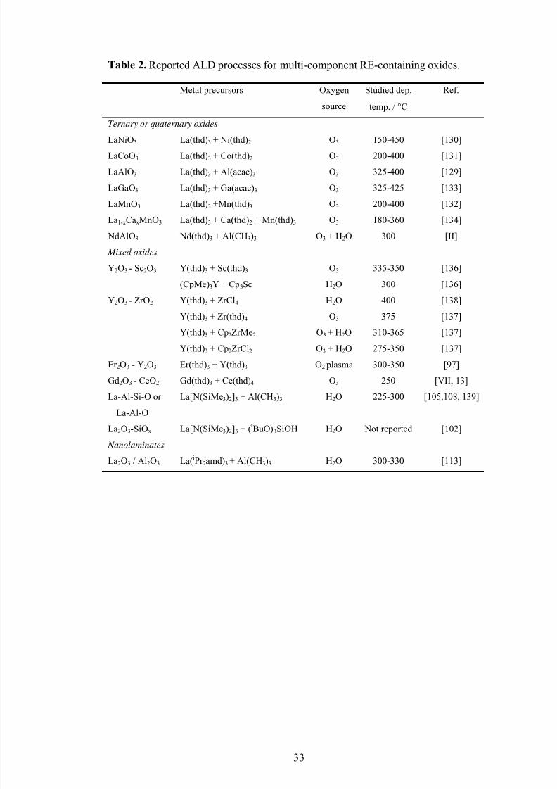
Table 2. Reported ALD processes for multi-component RE-containing oxides.
Metal precursors Oxygen
source
Studied dep.
temp. / °C
Ref.
Ternary or quaternary oxides
LaNiO3 La(thd)3 + Ni(thd)2 O3 150-450 [130]LaCoO3 La(thd)3 + Co(thd)2 O3 200-400 [131]
LaAlO3 La(thd)3 + Al(acac)3 O3 325-400 [129]
LaGaO3 La(thd)3 + Ga(acac)3 O3 325-425 [133]
LaMnO3 La(thd)3 +Mn(thd)3 O3 200-400 [132]
La1-xCaxMnO3 La(thd)3 + Ca(thd)2 + Mn(thd)3 O3 180-360 [134]
NdAlO3 Nd(thd)3 + Al(CH3)3 O3 + H2O 300 [II]
Mixed oxides
Y2O3 - Sc2O3 Y(thd)3 + Sc(thd)3 O3 335-350 [136]
(CpMe)3Y + Cp3Sc H2O 300 [136]
Y2O3 - ZrO2 Y(thd)3 + ZrCl4 H2O 400 [138]
Y(thd)3 + Zr(thd)4 O3 375 [137]
Y(thd)3 + Cp2ZrMe2 O3 + H2O 310-365 [137]
Y(thd)3 + Cp2ZrCl2 O3 + H2O 275-350 [137]
Er2O3 - Y2O3 Er(thd)3 + Y(thd)3 O2 plasma 300-350 [97]
Gd2O3 - CeO2 Gd(thd)3 + Ce(thd)4 O3 250 [VII, 13]
La-Al-Si-O or
La-Al-O
La[N(SiMe3)2]3 + Al(CH3)3 H2O 225-300 [105,108, 139]
La2O3-SiOx La[N(SiMe3)2]3 + (tBuO)3SiOH H2O Not reported [102]
Nanolaminates
La2O3 / Al2O3 La(iPr2amd)3 + Al(CH3)3 H2O 300-330 [113]
5/13/2018 ALD of Lanthanide Oxide Thin Films - slidepdf.com
http://slidepdf.com/reader/full/ald-of-lanthanide-oxide-thin-films 34/6934
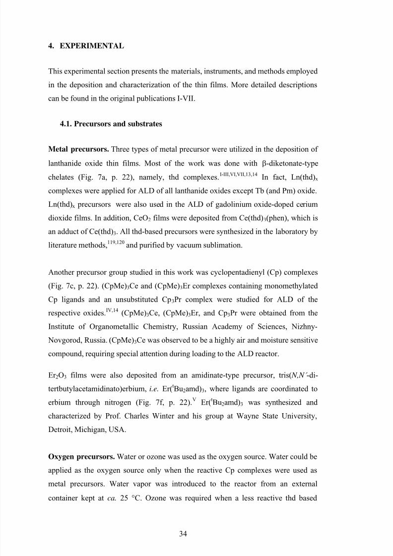
4. EXPERIMENTAL
This experimental section presents the materials, instruments, and methods employed
in the deposition and characterization of the thin films. More detailed descriptions
can be found in the original publications I-VII.
4.1. Precursors and substrates
Metal precursors. Three types of metal precursor were utilized in the deposition of
lanthanide oxide thin films. Most of the work was done with β-diketonate-type
chelates (Fig. 7a, p. 22), namely, thd complexes.I-III,VI,VII,13,14 In fact, Ln(thd)x
complexes were applied for ALD of all lanthanide oxides except Tb (and Pm) oxide.Ln(thd)x precursors were also used in the ALD of gadolinium oxide-doped cerium
dioxide films. In addition, CeO2 films were deposited from Ce(thd)3(phen), which is
an adduct of Ce(thd)3. All thd-based precursors were synthesized in the laboratory by
literature methods,119,120 and purified by vacuum sublimation.
Another precursor group studied in this work was cyclopentadienyl (Cp) complexes
(Fig. 7c, p. 22). (CpMe)3Ce and (CpMe)3Er complexes containing monomethylated
Cp ligands and an unsubstituted Cp3Pr complex were studied for ALD of the
respective oxides.IV,14 (CpMe)3Ce, (CpMe)3Er, and Cp3Pr were obtained from the
Institute of Organometallic Chemistry, Russian Academy of Sciences, Nizhny-
Novgorod, Russia. (CpMe)3Ce was observed to be a highly air and moisture sensitive
compound, requiring special attention during loading to the ALD reactor.
Er2O3 films were also deposited from an amidinate-type precursor, tris( N,N´ -di-
tertbutylacetamidinato)erbium, i.e. Er(tBu2amd)3, where ligands are coordinated toerbium through nitrogen (Fig. 7f, p. 22).V Er(tBu2amd)3 was synthesized and
characterized by Prof. Charles Winter and his group at Wayne State University,
Detroit, Michigan, USA.
Oxygen precursors. Water or ozone was used as the oxygen source. Water could be
applied as the oxygen source only when the reactive Cp complexes were used as
metal precursors. Water vapor was introduced to the reactor from an externalcontainer kept at ca. 25 °C. Ozone was required when a less reactive thd based
5/13/2018 ALD of Lanthanide Oxide Thin Films - slidepdf.com
http://slidepdf.com/reader/full/ald-of-lanthanide-oxide-thin-films 35/6935
precursor or the Er-amidinato complex was used as precursor. Ozone was produced
from >99.999% oxygen using a Fischer Model 502 ozone generator. The O3
concentration as determined by iodometric titration was approximately 4 %.140
Carrier and purge gases. Nitrogen was used as both carrier and purge gas in allexperiments. N2 was separated from air with a Nitrox UHPN 3000-1 nitrogen
generator employing molecular sieve technology and its purity was >99.999%.
Substrates. Most of the films were deposited on 5 cm × 5 cm Si(100) substrates of
p- or n-type, which were cut from larger wafers (∅ 150 mm) purchased from
Okmetic, Vantaa, Finland. The native oxide on the silicon was not removed before
deposition. Ultrasonically cleaned soda lime glass substrates of the same size wereusually used as well. However, the main focus of the studies was on the films
deposited on Si(100), and all the results presented in this thesis were obtained with
those films. CGO films were also deposited onto 2 cm × 2 cm pieces of typical
SOFC electrode materials Ni-YSZ and La1-xSrxMnO3 (LSM) obtained from InDEC
B.V. (Innovative Dutch Electroceramics), Petten, Netherlands.
4.2. Deposition of lanthanide oxide thin films
New ALD processes were developed for several binary lanthanide oxides (CeO2,
Nd2O3, Sm2O3, Eu2O3, Gd2O3, Dy2O3, Ho2O3, Er2O3, Tm2O3, Yb2O3, and Lu2O3) and
for the mixed oxide of Gd2O3 and CeO2, or Ce1-xGdxO2-0.5x (CGO). In addition, ALD
of PrOx was studied. Table 3 summarizes all the processes that were studied, while
the typical pulsing sequences used in this work are illustrated in Fig. 8. Depositions
were carried out in a satellite version of F-120 research-type ALD reactor (ASM
Microchemistry Ltd, Espoo, Finland). The pressure inside the reactor during
depositions was ca. 2−3 mbar.
5/13/2018 ALD of Lanthanide Oxide Thin Films - slidepdf.com
http://slidepdf.com/reader/full/ald-of-lanthanide-oxide-thin-films 36/6936
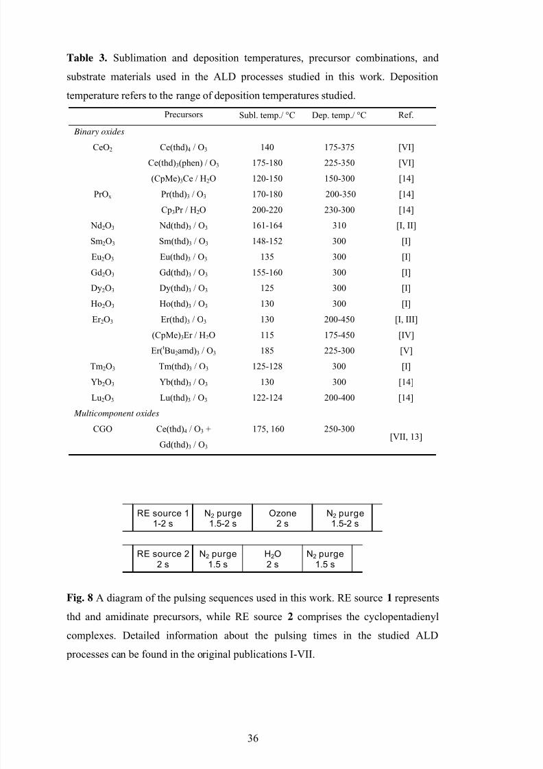
Table 3. Sublimation and deposition temperatures, precursor combinations, and
substrate materials used in the ALD processes studied in this work. Deposition
temperature refers to the range of deposition temperatures studied.
Precursors Subl. temp./ °C Dep. temp./ °C Ref.
Binary oxidesCeO2 Ce(thd)4 / O3 140 175-375 [VI]
Ce(thd)3(phen) / O3 175-180 225-350 [VI]
(CpMe)3Ce / H2O 120-150 150-300 [14]
PrOx Pr(thd)3 / O3 170-180 200-350 [14]
Cp3Pr / H2O 200-220 230-300 [14]
Nd2O3 Nd(thd)3 / O3 161-164 310 [I, II]
Sm2O3 Sm(thd)3 / O3 148-152 300 [I]
Eu2O3 Eu(thd)3 / O3 135 300 [I]
Gd2O3 Gd(thd)3 / O3 155-160 300 [I]
Dy2O3 Dy(thd)3 / O3 125 300 [I]
Ho2O3 Ho(thd)3 / O3 130 300 [I]
Er2O3 Er(thd)3 / O3 130 200-450 [I, III]
(CpMe)3Er / H2O 115 175-450 [IV]
Er(tBu2amd)3 / O3 185 225-300 [V]
Tm2O3 Tm(thd)3 / O3 125-128 300 [I]
Yb2O3 Yb(thd)3 / O3 130 300 [14]
Lu2O
3Lu(thd)
3/ O
3122-124 200-400 [14]
Multicomponent oxides
CGO Ce(thd)4 / O3 +
Gd(thd)3 / O3
175, 160 250-300[VII, 13]
N2 purge 1.5-2 s
N2 purge1.5-2 s
Ozone2 s
RE source 1 1-2 s
N2 purge 1.5 s
N2 purge1.5 s
H2O2 s
RE source 2 2 s
Fig. 8 A diagram of the pulsing sequences used in this work. RE source 1 represents
thd and amidinate precursors, while RE source 2 comprises the cyclopentadienyl
complexes. Detailed information about the pulsing times in the studied ALD
processes can be found in the original publications I-VII.
5/13/2018 ALD of Lanthanide Oxide Thin Films - slidepdf.com
http://slidepdf.com/reader/full/ald-of-lanthanide-oxide-thin-films 37/6937
The preferred stoichiometry and structure of cerium and praseodymium oxides differ
from those of other lanthanide oxides studied in this work. This is due to the higher
stability of the oxidation state +IV in cerium and praseodymium compounds.1-3
Cerium preferentially forms fluorite-structured CeO2, whereas the stoichiometry of
praseodymium oxide, PrOx depends on the prevailing conditions. In fact,praseodymium can form series of intermediate oxides, PrnO2n-2m, having fluorite
structure. The depositions of CeO2, PrOx, and CGO films are presented in separately
(Section 4.2.3) since they differed from those of the Ln2O3 series.
4.2.1. Ln(thd)3 /O3 process for Ln2O3 films
Among the thd-based ALD processes developed for the Ln2O3 series, only the
growth of Nd2O3, Er2O3, and Lu2O3 films was fully evaluated over a wide
temperature range and with different pulsing times of the precursors.II,III,14 In the
depositions of other Ln2O3 films (Ln = Sm, Eu, Gd, Dy, Ho, Tm, and Yb), the
precursor sublimation temperatures and pulsing times were not optimized but merely
set to obtain sufficient precursor flow and surface saturation during the film growth.I
Furthermore, substrate temperature of 300 °C was used in these depositions because,
from the reported ALD processes for RE2O3 (RE = Y, La, Nd, or Er),90,93,II,III it was
clear that the ALD windows of RE(thd)3 /O3 processes are around 300 °C. The
thicknesses of the Ln2O3 films were adjusted to approximately 50 nm to allow
meaningful comparison of the film characteristics, such as purity, roughness,
crystallinity, and relative permittivity.I
The sublimation temperatures of Ln(thd)3 precursors were observed to decrease
toward the heavier lanthanides, from 161−164 °C for Nd(thd)3 to 122 °C for
Lu(thd)3. The higher volatility of heavier Ln(thd)3 complexes has been reported
earlier.117,141 Although this finding might at first appear surprising it can be explained
in terms of the lanthanide contraction. The smaller size of the heavier lanthanide ions
makes their complexes less susceptible to intermolecular interactions such as
dimerization and oligomerization, which reduce volatility.114
5/13/2018 ALD of Lanthanide Oxide Thin Films - slidepdf.com
http://slidepdf.com/reader/full/ald-of-lanthanide-oxide-thin-films 38/6938
4.2.2. Processes for Er2O3 films
Er2O3 films were deposited using three different metal precursors.III-V In addition to
the Er(thd)3 complex, study was made of organometallic (CpMe)3Er and nitrogen-
coordinated Er(t
Bu2amd)3. Er2O3 film growth was carefully studied in each processover a wide deposition temperature range and with different pulsing times of the
precursors. The suitability of the different precursors for ALD of lanthanide oxides
was then evaluated.
Water was used as the oxygen source in the (CpMe)3Er process, but ozone with
Er(thd)3 and Er(tBu2amd)3, which do not react with water. Use of water may be
preferred for gate dielectric applications since ozone reportedly reacts with HF-
etched silicon substrate to form an 1.1−1.4 nm thick interfacial SiOx layer,91,142,143
thus increasing the EOT value. This may not be so critical, however, because it might
be preferable to have a very thin SiO2 layer on the Si substrate to obtain dielectric
layer of high quality and yet a low EOT value (<1 nm).144 It has namely been
reported that the HfCl4 /H2O process yielded non-uniform HfO2 films with poor
electrical properties when deposited on H-terminated Si, but high quality films with
good electrical properties were obtained when Si substrates had a thin thermally
grown SiO2 layer on top.145 Additionally, in some comparative studies it has even
been reported that H2O and O3 form equally thick interfacial SiOx layers on HF-
etched silicon.142,146
4.2.3. ALD of CeO2, Ce1-xGdxO2-0.5x, and PrOx films
In the ALD of CeO2 films, two different β-diketonate compounds, Ce(thd)4 and
Ce(thd)3(phen), were successfully employed as Ce precursors, while ozone was used
as the oxygen source. The temperature range studied was 175−375 °C for Ce(thd)4
and 225−350 °C for Ce(thd)3(phen). The effect of pulse and purge times was
investigated as well.VI ALD of CeO2 films was further studied with (CpMe)3Ce as
precursor and a deposition temperature range of 150−300 °C.14
5/13/2018 ALD of Lanthanide Oxide Thin Films - slidepdf.com
http://slidepdf.com/reader/full/ald-of-lanthanide-oxide-thin-films 39/6939
The ALD process for Ce1-xGdxO2-0.5x (CGO) filmsVII,13 was developed by combining
the binary Ce(thd)4 /O3V and Gd(thd)3 /O3
I,95 processes. The deposition temperature
was selected to be 250 °C, which is inside the ALD windows of both binary
processes.VI,95 The aim was to deposit films having the stoichiometry of
Ce0.9Gd0.1O1.95, and where the conductivity of CGO is highest.33 CGO films werefirst deposited on Si(100) substrates to define the dependence of the film
stoichiometry on the pulsing ratio of the precursors. Pulsing ratios of Ce(thd)4 and
Gd(thd)3 varying from 3:1 to 19:1 were studied. Actual samples for SOFCs were
then grown on typical electrode materials: Ni-YSZ cermet and
La1-xSrxMnO3 (LSM). CGO films were up to 1 µm thick and thus considerably
thicker than films in any other study in this work. For comparison, CGO thin films
were also prepared by sputtering, and results were compared with those for the ALD-grown films.VII,13
Two different precursors were tested for the ALD of PrOx thin films, namely Pr(thd)3
and Cp3Pr. The temperature ranges studied were 200−350 °C in the Pr(thd)3 /O3
process and 230−300 °C in the Cp3Pr/H2O process.14
4.3. Film characterization
Various analytical techniques were employed for characterization of the thin films.
Film thicknesses were determined by fitting the transmittance or reflectance spectra
measured with a Hitachi U-2000 spectrophotometer.147 In some cases, thickness of
the very thin films was also measured with a Bruker D8 Advance X-ray
diffractometer set in the X-ray reflection mode (XRR).
An X-ray diffractometer (Philips MPD 1880) with Cu-Kα radiation was used to
determine the crystallinity and crystallite orientation of the films. Fourier transform
infrared spectroscopic (FTIR) measurements (Nicolet Magna-IR 750) were carried
out to obtain information about hydroxide and carbonate impurities in the films. The
contribution of the Si substrate was subtracted from the measured spectra.
5/13/2018 ALD of Lanthanide Oxide Thin Films - slidepdf.com
http://slidepdf.com/reader/full/ald-of-lanthanide-oxide-thin-films 40/6940
Film morphology and uniformity were examined by atomic force microscopy
(AFM). A Nanoscope III (Digital Instruments) was used in the AFM measurements
and it was operated in tapping mode with a scanning rate of 1−2 Hz. Large area
images (10 µm × 10 µm) were measured from different parts of the films to ascertain
the uniformity, while final images were taken using a scanning area of 2µm × 2 µm.Surface roughnesses were calculated as root mean square (rms) values. Furthermore,
film composition and stoichiometry were determined by time-of-flight elastic recoil
detection analysis (TOF-ERDA).148,149 A 53 MeV 127I10+ ion beam produced in a 5
MV tandem accelerator EGP-10-II was used in TOF-ERD analyses.
Ce1-xGdxO2-0.5x films were analyzed by combined use of a secondary electron
microscope (SEM) and an energy dispersive X-ray spectroscope (EDS) to obtaininformation about uniformity, density, and stoichiometry. Leica S440 and Tracor-
Noran Voyager 1 instruments were used in the SEM and EDS analyses, respectively.
Electrical properties of the dielectric Ln2O3 films were analyzed with use of a HP
4284A precision LCR meter for capacitance-voltage (C-V) and a Keitley 2400
Source Meter for current-voltage (I-V) measurements. Al/Ln2O3 /native SiO2 /n-
Si(100)/Al structures for the electrical measurements were prepared by depositingaluminum dots onto the dielectric film surface and an Al-contact layer onto the
backside of the Si(100) substrate by electron beam evaporation. The native oxide
layer on the backside of the Si(100) substrate was HF-etched before evaporation to
achieve ohmic contact between Si and Al. A voltage step of 0.05 V and ac signal
frequency of 100 kHz or 500 kHz were used in C-V measurements. A voltage step of
0.05 V was applied in the I-V measurements. Both C-V and I-V measurements were
carried out at room temperature and under normal pressure. Electrical conductivity of
the CGO films was measured by impedance spectroscopy using an Autolab
PGSTAT30 instrument manufactured by Ecochemie BV.
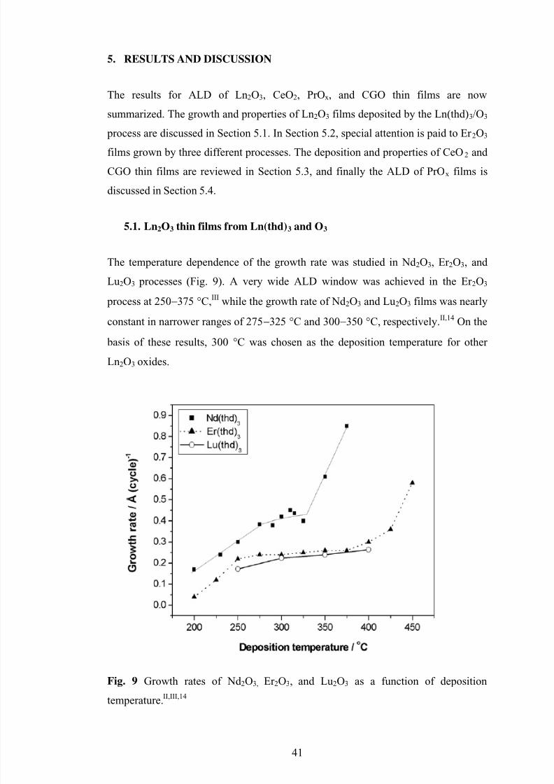
5/13/2018 ALD of Lanthanide Oxide Thin Films - slidepdf.com
http://slidepdf.com/reader/full/ald-of-lanthanide-oxide-thin-films 41/6941
5. RESULTS AND DISCUSSION
The results for ALD of Ln2O3, CeO2, PrOx, and CGO thin films are now
summarized. The growth and properties of Ln2O3 films deposited by the Ln(thd)3 /O3
process are discussed in Section 5.1. In Section 5.2, special attention is paid to Er2O3 films grown by three different processes. The deposition and properties of CeO2 and
CGO thin films are reviewed in Section 5.3, and finally the ALD of PrOx films is
discussed in Section 5.4.
5.1. Ln2O3 thin films from Ln(thd)3 and O3
The temperature dependence of the growth rate was studied in Nd2O3, Er2O3, and
Lu2O3 processes (Fig. 9). A very wide ALD window was achieved in the Er2O3
process at 250−375 °C,III while the growth rate of Nd2O3 and Lu2O3 films was nearly
constant in narrower ranges of 275−325 °C and 300−350 °C, respectively.II,14 On the
basis of these results, 300 °C was chosen as the deposition temperature for other
Ln2O3 oxides.
Fig. 9 Growth rates of Nd2O3, Er2O3, and Lu2O3 as a function of depositiontemperature.II,III,14
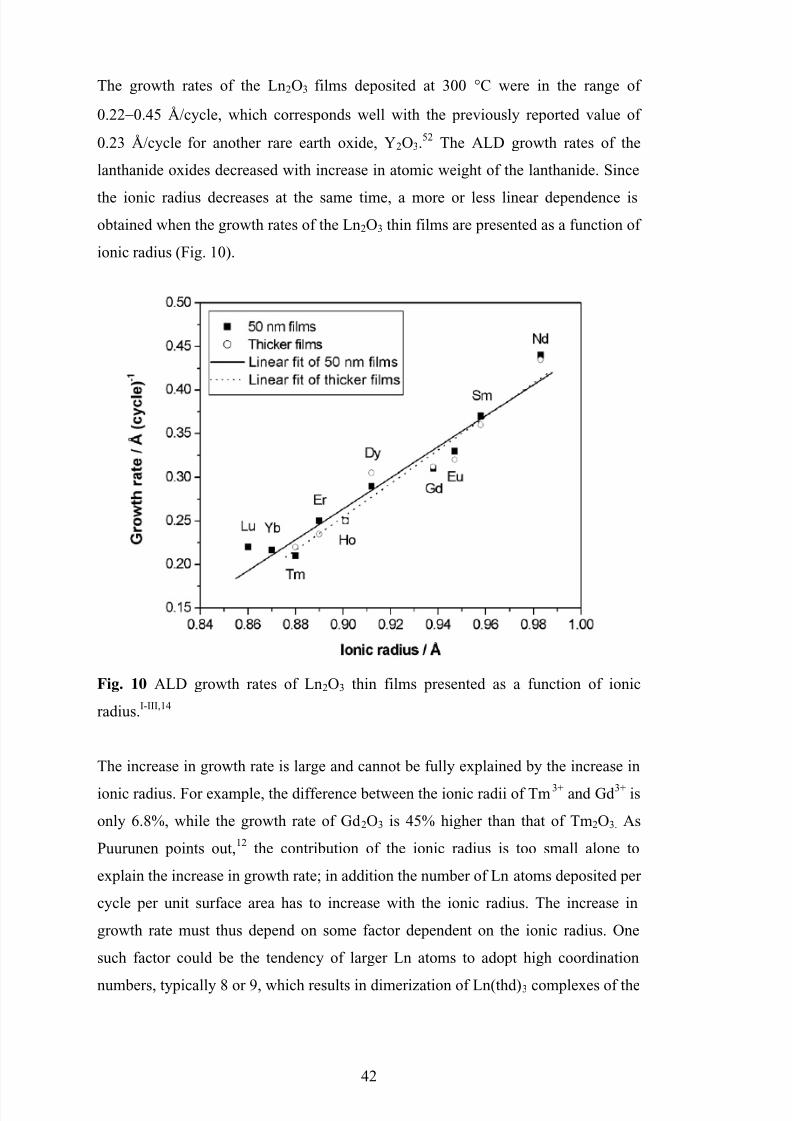
5/13/2018 ALD of Lanthanide Oxide Thin Films - slidepdf.com
http://slidepdf.com/reader/full/ald-of-lanthanide-oxide-thin-films 42/6942
The growth rates of the Ln2O3 films deposited at 300 °C were in the range of
0.22−0.45 Å/cycle, which corresponds well with the previously reported value of
0.23 Å/cycle for another rare earth oxide, Y2O3.52 The ALD growth rates of the
lanthanide oxides decreased with increase in atomic weight of the lanthanide. Since
the ionic radius decreases at the same time, a more or less linear dependence isobtained when the growth rates of the Ln2O3 thin films are presented as a function of
ionic radius (Fig. 10).
Fig. 10 ALD growth rates of Ln2O3 thin films presented as a function of ionic
radius.I-III,14
The increase in growth rate is large and cannot be fully explained by the increase in
ionic radius. For example, the difference between the ionic radii of Tm3+ and Gd3+ is
only 6.8%, while the growth rate of Gd2O3 is 45% higher than that of Tm2O3. As
Puurunen points out,12 the contribution of the ionic radius is too small alone to
explain the increase in growth rate; in addition the number of Ln atoms deposited per
cycle per unit surface area has to increase with the ionic radius. The increase in
growth rate must thus depend on some factor dependent on the ionic radius. One
such factor could be the tendency of larger Ln atoms to adopt high coordination
numbers, typically 8 or 9, which results in dimerization of Ln(thd)3 complexes of the
5/13/2018 ALD of Lanthanide Oxide Thin Films - slidepdf.com
http://slidepdf.com/reader/full/ald-of-lanthanide-oxide-thin-films 43/6943
larger lanthanides (Ln = La-Gd).114,150-152 Complexes of the smaller lanthanides are
monomeric.114,152,153 Such behavior could result in different reactions on the substrate
surface. It is not clear what other factors might contribute to the observed trend in
growth rate and therefore the ionic radius is the most informative choice at this point.
X-ray diffraction showed the Ln2O3 thin films to have a polycrystalline, cubic
structure. Films deposited at temperatures close to 300 °C preferred the (100)
orientation, as (400) was the strongest observed reflection. Minor (222), (411), (440),
(611), and (622) reflections were also detected, as can be seen from the diffraction
pattern of Tm2O3 presented in Fig. 11a. At 250 °C and below, all studied films were
amorphous or only weakly crystalline.I-III Studies with Er2O3 and Lu2O3 showed that,
as the deposition temperature was increased, films became more crystalline and therelative intensities of the reflections changed, the (222) reflection being the strongest
one above 350 °C (Fig. 11b).III,14 The same kind of behavior has been reported for
Sc2O3 and Y2O3 films grown by the RE(thd)3 /O3 ALD process when the deposition
temperature was increased from 300 °C to 375 °C.89,90 In the Nd2O3 films, however,
(100) remained the dominant orientation at all deposition temperatures where
crystalline films were obtained (>250 °C).
Lanthanide oxides are basic materials, which become hydrated and carbonated when
exposed to atmospheric water and carbon dioxide.1-3 The basicity increases toward
the lighter lanthanides. Neodymium is the lightest of the lanthanides studied in this
work, and this may explain why the results for Nd2O3 films were somewhat different
from those obtained for the other Ln2O3 films. For example, the XRD experiments
revealed that Nd2O3 films react with ambient air during storage and NdO(OH) is
formed (Fig. 11c).II
The formation of NdO(OH) was also observed in FTIRexperiments, where an absorption band around 3435 cm-1 could be assigned to
stretching of the hydroxide group. The tendency of Nd2O3 films to absorb water
seemed to be related to the amount of carbon impurity in the films. Namely, as the
deposition temperature of the Nd2O3 films was increased, the carbon concentration
decreased (according to FTIR), and at the same time the films became more reactive
toward atmospheric moisture. A similar tendency has been reported for ALD-grown
La2O3 films,93 but no formation of the LnO(OH) phase was observed for the heavier
lanthanide oxides studied here.I
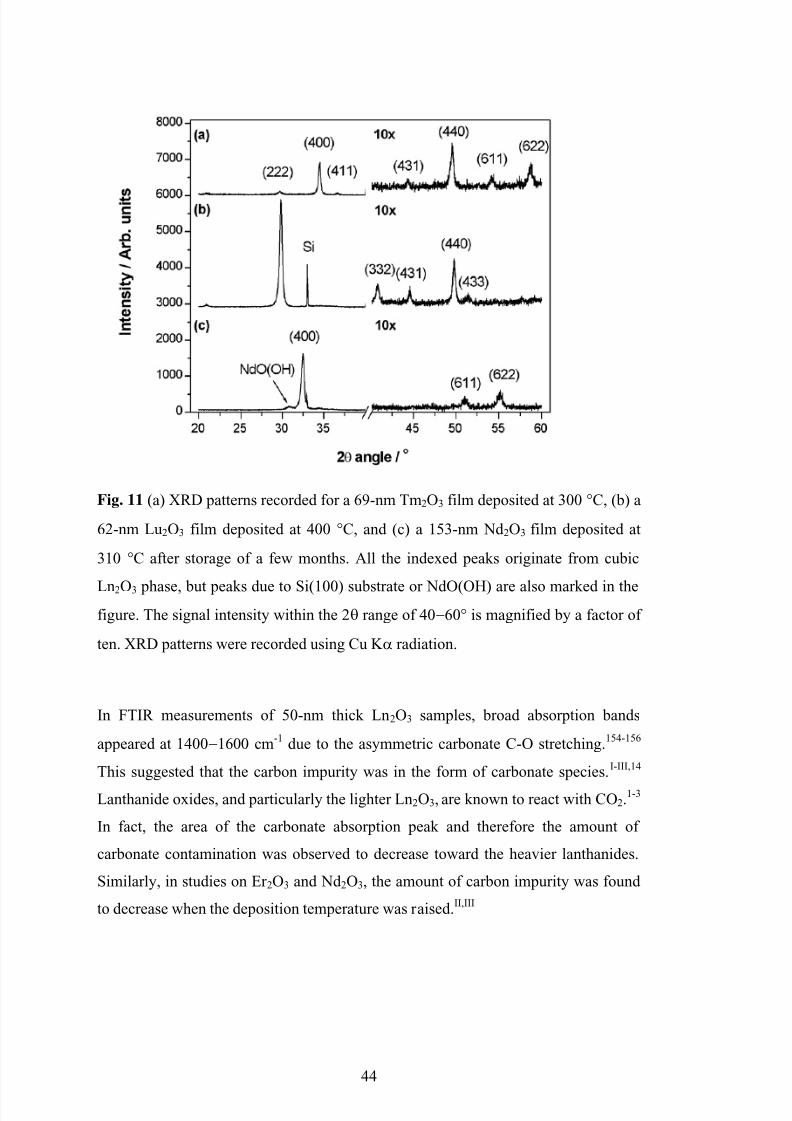
5/13/2018 ALD of Lanthanide Oxide Thin Films - slidepdf.com
http://slidepdf.com/reader/full/ald-of-lanthanide-oxide-thin-films 44/6944
Fig. 11 (a) XRD patterns recorded for a 69-nm Tm2O3 film deposited at 300 °C, (b) a
62-nm Lu2O3 film deposited at 400 °C, and (c) a 153-nm Nd2O3 film deposited at
310 °C after storage of a few months. All the indexed peaks originate from cubic
Ln2O3 phase, but peaks due to Si(100) substrate or NdO(OH) are also marked in thefigure. The signal intensity within the 2θ range of 40−60° is magnified by a factor of
ten. XRD patterns were recorded using Cu Kα radiation.
In FTIR measurements of 50-nm thick Ln2O3 samples, broad absorption bands
appeared at 1400−1600 cm-1 due to the asymmetric carbonate C-O stretching.154-156
This suggested that the carbon impurity was in the form of carbonate species.I-III,14
Lanthanide oxides, and particularly the lighter Ln2O3, are known to react with CO2.1-3
In fact, the area of the carbonate absorption peak and therefore the amount of
carbonate contamination was observed to decrease toward the heavier lanthanides.
Similarly, in studies on Er2O3 and Nd2O3, the amount of carbon impurity was found
to decrease when the deposition temperature was raised.II,III
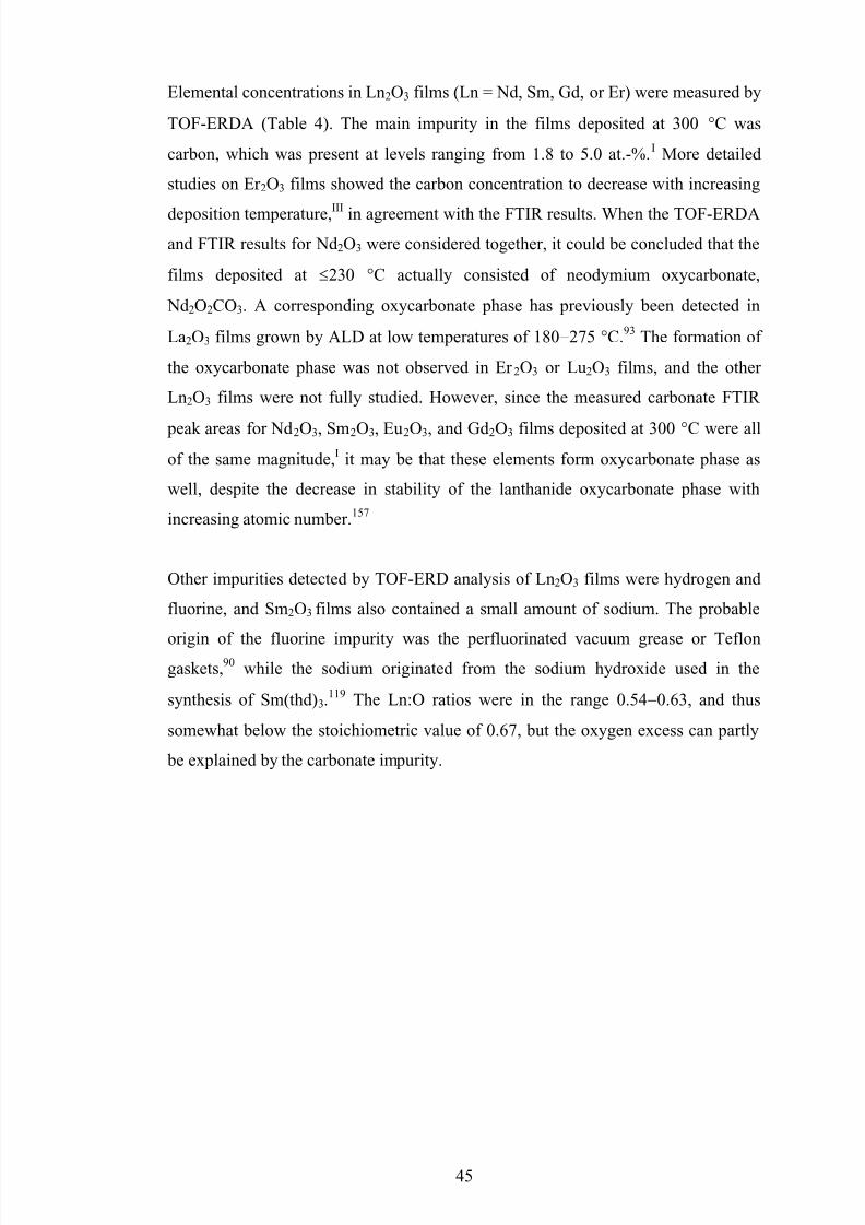
5/13/2018 ALD of Lanthanide Oxide Thin Films - slidepdf.com
http://slidepdf.com/reader/full/ald-of-lanthanide-oxide-thin-films 45/6945
Elemental concentrations in Ln2O3 films (Ln = Nd, Sm, Gd, or Er) were measured by
TOF-ERDA (Table 4). The main impurity in the films deposited at 300 °C was
carbon, which was present at levels ranging from 1.8 to 5.0 at.-%.I More detailed
studies on Er2O3 films showed the carbon concentration to decrease with increasing
deposition temperature,III in agreement with the FTIR results. When the TOF-ERDAand FTIR results for Nd2O3 were considered together, it could be concluded that the
films deposited at ≤230 °C actually consisted of neodymium oxycarbonate,
Nd2O2CO3. A corresponding oxycarbonate phase has previously been detected in
La2O3 films grown by ALD at low temperatures of 180−275 °C.93 The formation of
the oxycarbonate phase was not observed in Er2O3 or Lu2O3 films, and the other
Ln2O3 films were not fully studied. However, since the measured carbonate FTIR
peak areas for Nd2O3, Sm2O3, Eu2O3, and Gd2O3 films deposited at 300 °C were allof the same magnitude,I it may be that these elements form oxycarbonate phase as
well, despite the decrease in stability of the lanthanide oxycarbonate phase with
increasing atomic number.157
Other impurities detected by TOF-ERD analysis of Ln2O3 films were hydrogen and
fluorine, and Sm2O3 films also contained a small amount of sodium. The probable
origin of the fluorine impurity was the perfluorinated vacuum grease or Teflongaskets,90 while the sodium originated from the sodium hydroxide used in the
synthesis of Sm(thd)3.119 The Ln:O ratios were in the range 0.54−0.63, and thus
somewhat below the stoichiometric value of 0.67, but the oxygen excess can partly
be explained by the carbonate impurity.
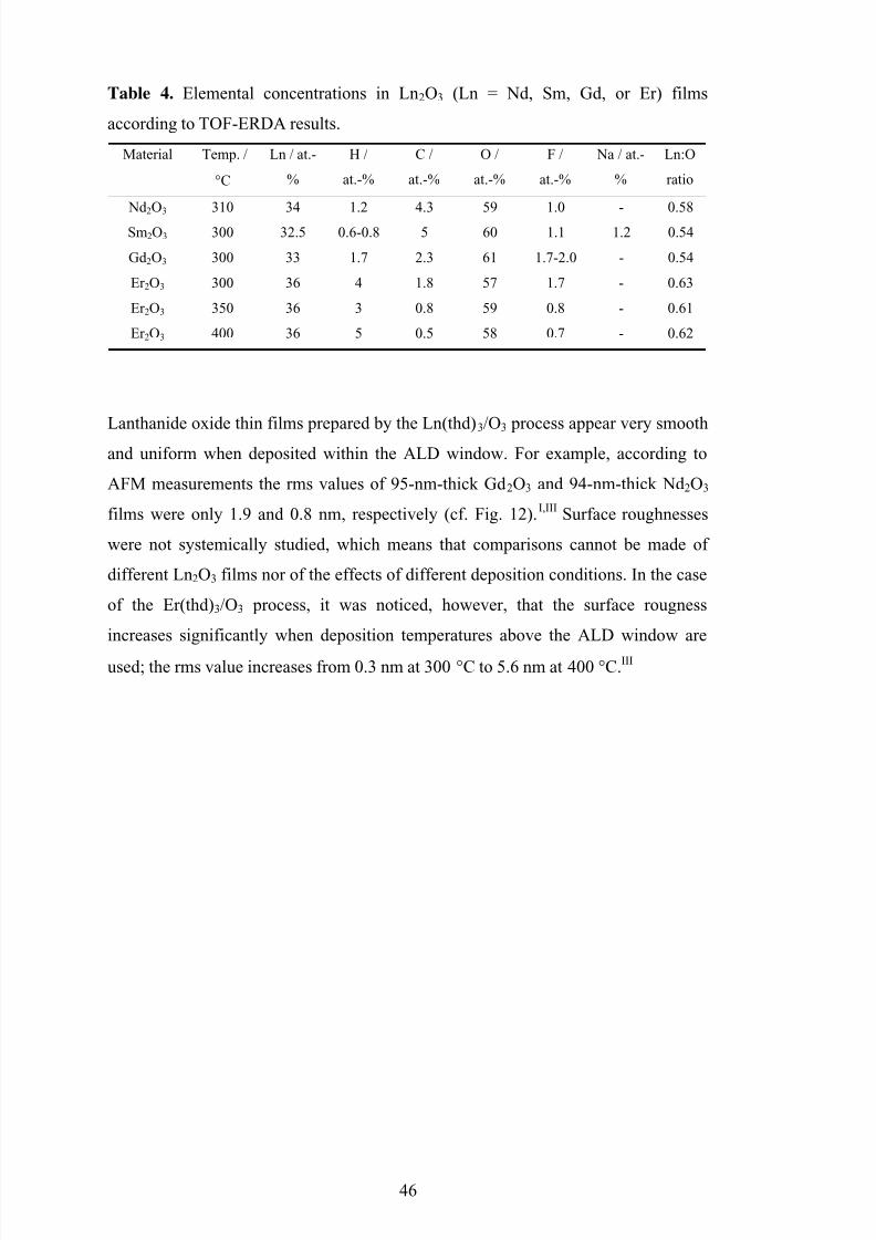
5/13/2018 ALD of Lanthanide Oxide Thin Films - slidepdf.com
http://slidepdf.com/reader/full/ald-of-lanthanide-oxide-thin-films 46/6946
Table 4. Elemental concentrations in Ln2O3 (Ln = Nd, Sm, Gd, or Er) films
according to TOF-ERDA results.
Material Temp. /
°C
Ln / at.-
%
H /
at.-%
C /
at.-%
O /
at.-%
F /
at.-%
Na / at.-
%
Ln:O
ratio
Nd2O3 310 34 1.2 4.3 59 1.0 - 0.58
Sm2O3 300 32.5 0.6-0.8 5 60 1.1 1.2 0.54
Gd2O3 300 33 1.7 2.3 61 1.7-2.0 - 0.54
Er2O3 300 36 4 1.8 57 1.7 - 0.63
Er2O3 350 36 3 0.8 59 0.8 - 0.61
Er2O3 400 36 5 0.5 58 0.7 - 0.62
Lanthanide oxide thin films prepared by the Ln(thd)3 /O
3process appear very smooth
and uniform when deposited within the ALD window. For example, according to
AFM measurements the rms values of 95-nm-thick Gd2O3 and 94-nm-thick Nd2O3
films were only 1.9 and 0.8 nm, respectively (cf. Fig. 12).I,III Surface roughnesses
were not systemically studied, which means that comparisons cannot be made of
different Ln2O3 films nor of the effects of different deposition conditions. In the case
of the Er(thd)3 /O3 process, it was noticed, however, that the surface rougness
increases significantly when deposition temperatures above the ALD window are
used; the rms value increases from 0.3 nm at 300 °C to 5.6 nm at 400 °C.III
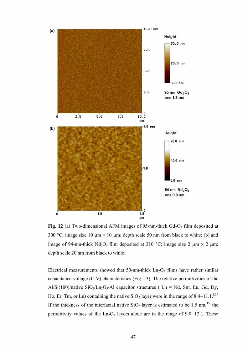
5/13/2018 ALD of Lanthanide Oxide Thin Films - slidepdf.com
http://slidepdf.com/reader/full/ald-of-lanthanide-oxide-thin-films 47/6947
Fig. 12 (a) Two-dimensional AFM images of 95-nm-thick Gd2O3 film deposited at
300 °C; image size 10 µm × 10 µm; depth scale 50 nm from black to white; (b) and
image of 94-nm-thick Nd2O3 film deposited at 310 °C; image size 2 µm × 2 µm;depth scale 20 nm from black to white.
Electrical measurements showed that 50-nm-thick Ln2O3 films have rather similar
capacitance-voltage (C-V) characteristics (Fig. 13). The relative permittivities of the
Al/Si(100)/native SiO2 /Ln2O3 /Al capacitor structures ( Ln = Nd, Sm, Eu, Gd, Dy,
Ho, Er, Tm, or Lu) containing the native SiO2 layer were in the range of 8.4−11.1.I,14
If the thickness of the interfacial native SiO2 layer is estimated to be 1.5 nm,IV
thepermittivity values of the Ln2O3 layers alone are in the range of 9.0−12.1. These
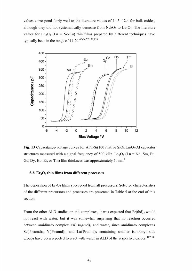
5/13/2018 ALD of Lanthanide Oxide Thin Films - slidepdf.com
http://slidepdf.com/reader/full/ald-of-lanthanide-oxide-thin-films 48/6948
values correspond fairly well to the literature values of 14.3−12.4 for bulk oxides,
although they did not systematically decrease from Nd2O3 to Lu2O3. The literature
values for Ln2O3 (Ln = Nd-Lu) thin films prepared by different techniques have
typically been in the range of 11-20.60-66,77,158,159
Fig. 13 Capacitance-voltage curves for Al/n-Si(100)/native SiO2 /Ln2O3 /Al capacitor
structures measured with a signal frequency of 500 kHz. Ln2O3 (Ln = Nd, Sm, Eu,
Gd, Dy, Ho, Er, or Tm) film thickness was approximately 50 nm.I
5.2. Er2O3 thin films from different processes
The deposition of Er2O3 films succeeded from all precursors. Selected characteristics
of the different precursors and processes are presented in Table 5 at the end of this
section.
From the other ALD studies on thd complexes, it was expected that Er(thd)3 would
not react with water, but it was somewhat surprising that no reaction occurred
between amidinato complex Er(tBu2amd)3 and water, since amidinato complexes
Sc(iPr2amd)3, Y(iPr2amd)3, and La(iPr2amd)3 containing smaller isopropyl side
groups have been reported to react with water in ALD of the respective oxides.109-111
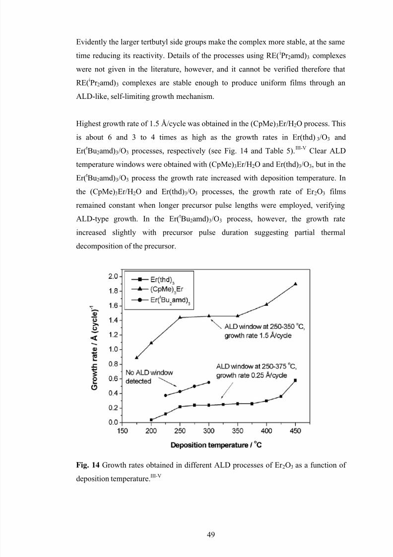
5/13/2018 ALD of Lanthanide Oxide Thin Films - slidepdf.com
http://slidepdf.com/reader/full/ald-of-lanthanide-oxide-thin-films 49/6949
Evidently the larger tertbutyl side groups make the complex more stable, at the same
time reducing its reactivity. Details of the processes using RE(iPr2amd)3 complexes
were not given in the literature, however, and it cannot be verified therefore that
RE(iPr2amd)3 complexes are stable enough to produce uniform films through an
ALD-like, self-limiting growth mechanism.
Highest growth rate of 1.5 Å/cycle was obtained in the (CpMe)3Er/H2O process. This
is about 6 and 3 to 4 times as high as the growth rates in Er(thd)3 /O3 and
Er(tBu2amd)3 /O3 processes, respectively (see Fig. 14 and Table 5).III-V Clear ALD
temperature windows were obtained with (CpMe)3Er/H2O and Er(thd)3 /O3, but in the
Er(tBu2amd)3 /O3 process the growth rate increased with deposition temperature. In
the (CpMe)3Er/H2O and Er(thd)3 /O3 processes, the growth rate of Er2O3 filmsremained constant when longer precursor pulse lengths were employed, verifying
ALD-type growth. In the Er(tBu2amd)3 /O3 process, however, the growth rate
increased slightly with precursor pulse duration suggesting partial thermal
decomposition of the precursor.
Fig. 14 Growth rates obtained in different ALD processes of Er2O3 as a function of
deposition temperature.III-V
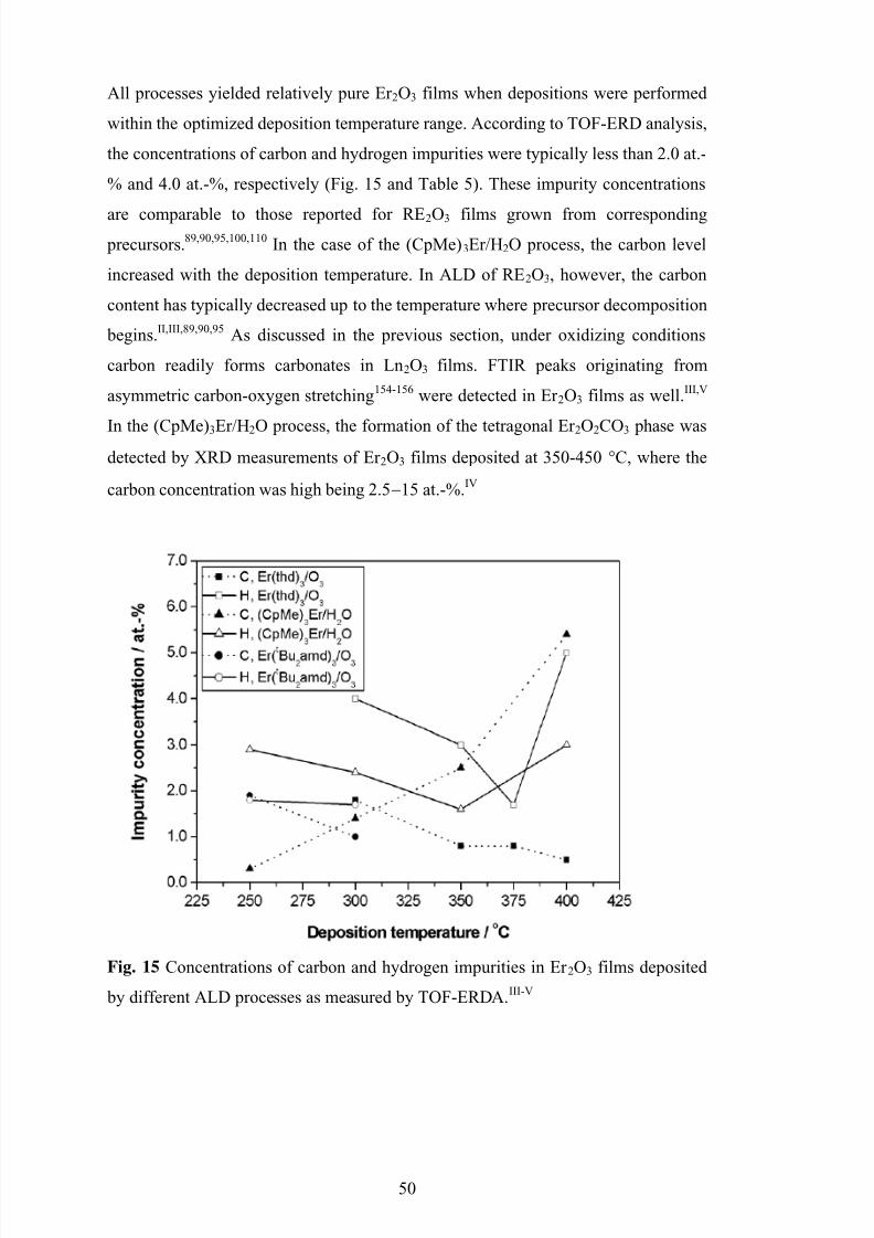
5/13/2018 ALD of Lanthanide Oxide Thin Films - slidepdf.com
http://slidepdf.com/reader/full/ald-of-lanthanide-oxide-thin-films 50/6950
All processes yielded relatively pure Er2O3 films when depositions were performed
within the optimized deposition temperature range. According to TOF-ERD analysis,
the concentrations of carbon and hydrogen impurities were typically less than 2.0 at.-
% and 4.0 at.-%, respectively (Fig. 15 and Table 5). These impurity concentrations
are comparable to those reported for RE2O3 films grown from correspondingprecursors.89,90,95,100,110 In the case of the (CpMe)3Er/H2O process, the carbon level
increased with the deposition temperature. In ALD of RE2O3, however, the carbon
content has typically decreased up to the temperature where precursor decomposition
begins.II,III,89,90,95 As discussed in the previous section, under oxidizing conditions
carbon readily forms carbonates in Ln2O3 films. FTIR peaks originating from
asymmetric carbon-oxygen stretching154-156 were detected in Er2O3 films as well.III,V
In the (CpMe)3Er/H2O process, the formation of the tetragonal Er2O2CO3 phase wasdetected by XRD measurements of Er2O3 films deposited at 350-450 °C, where the
carbon concentration was high being 2.5−15 at.-%.IV
Fig. 15 Concentrations of carbon and hydrogen impurities in Er2O3 films deposited
by different ALD processes as measured by TOF-ERDA.III-V
5/13/2018 ALD of Lanthanide Oxide Thin Films - slidepdf.com
http://slidepdf.com/reader/full/ald-of-lanthanide-oxide-thin-films 51/6951
Crystallinity of the Er2O3 films differed slightly according to the process. The as-
deposited films grown by Er(thd)3 /O3 and Er(tBu2amd)3 /O3 processes were
amorphous at deposition temperatures below 250 °C, but they were polycrystalline
cubic Er2O3 with the (100) orientation dominant when deposited at 250−350 °C. The
(CpMe)3Er/H2O process, in turn, consistently gave polycrystalline films, the (222)crystal plane showing the strongest reflection throughout the deposition temperature
range studied. The (100) and (111) orientations of the cubic Ln2O3 phase have been
the dominant ones in all previously reported ALD processes as well. Inside the ALD
windows of these processes, i.e. at deposition temperatures around 300 °C, the
RE(thd)3 /O3 process (RE = Y, La, or Nd-Lu)I-III,90,95 seems to prefer the (100)
orientation, but in the case of scandium, which is the smallest RE element, the thd
process resulted in (111) oriented Sc2O3 films.89
The (111) orientation is alsotypically preferred in RE2O3 films (RE = Sc, Y, Gd, or Er) grown from
cyclopentadienyl precursors.IV,89,90,95 Where other types of precursors have been
used, the dominant orientation in Ln2O3 has been (100) in Er2O3 from Er(tBu2amd)3,V
(111) in Gd2O3 from Gd(mmp)3,99 and both (111) and (100) in Y2O3 from
Y(iPr2amd)3.110 The precursor therefore influences the growth mode, and furthermore
the orientation of ALD grown films. As noted above, however, in the thd processes
the size of the RE ion plays a role as well.
Electrical properties of the 50-nm and 12.5-nm thick Er2O3 films grown by the
Er(thd)3 /O3 and (CpMe)3Er/H2O processes, respectively, were analyzed for
permittivity. Films were deposited onto Si(100) substrates covered by a native SiO2
layer. In both cases, the relative permittivity of the measured Al/Er2O3 /native SiO2 /p-
Si(100)/Al structures was 10. The relative permittivity of the Er2O3 layer can only be
evaluated if the thickness of the native SiO2
layer is known. According to XRR
measurements, the SiO2 layer in films grown by the (CpMe)3Er/H2O process was ca.
1.5 nm thick.IV Thus the relative permittivity values were 14.5 and 10.8 for the Er2O3
samples deposited by the (CpMe)3Er/H2O and Er(thd)3 /O3 processes, respectively.
Previously, Mikhelasvili et al.63 have reported relative permittivity values of 6.8 for
6.5-nm-thick and 14 for 50-nm Er2O3 films deposited by EBE.
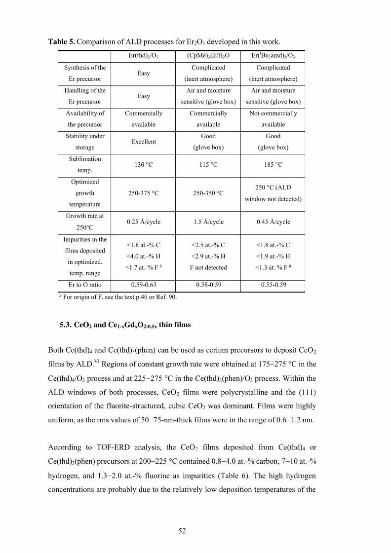
5/13/2018 ALD of Lanthanide Oxide Thin Films - slidepdf.com
http://slidepdf.com/reader/full/ald-of-lanthanide-oxide-thin-films 52/6952
Table 5. Comparison of ALD processes for Er2O3 developed in this work.
Er(thd)3 /O3 (CpMe)3Er/H2O Er(tBu2amd)3 /O3
Synthesis of the
Er precursorEasy
Complicated
(inert atmosphere)
Complicated
(inert atmosphere)
Handling of the
Er precursor Easy
Air and moisture
sensitive (glove box)
Air and moisture
sensitive (glove box)
Availability of
the precursor
Commercially
available
Commercially
available
Not commercially
available
Stability under
storageExcellent
Good
(glove box)
Good
(glove box)
Sublimation
temp.130 °C 115 °C 185 °C
Optimized
growthtemperature
250-375 °C 250-350 °C
250 °C (ALD
window not detected)
Growth rate at
250°C0.25 Å/cycle 1.5 Å/cycle 0.45 Å/cycle
Impurities in the
films deposited
in optimized.
temp. range
<1.8 at.-% C
<4.0 at.-% H
<1.7 at.-% F a
<2.5 at.-% C
<2.9 at.-% H
F not detected
<1.8 at.-% C
<1.9 at.-% H
<1.3 at. % F a
Er to O ratio 0.59-0.63 0.58-0.59 0.55-0.59a For origin of F, see the text p.46 or Ref. 90.
5.3. CeO2 and Ce1-xGdxO2-0.5x thin films
Both Ce(thd)4 and Ce(thd)3(phen) can be used as cerium precursors to deposit CeO2
films by ALD.VI Regions of constant growth rate were obtained at 175−275 °C in the
Ce(thd)4 /O3 process and at 225−275 °C in the Ce(thd)3(phen)/O3 process. Within the
ALD windows of both processes, CeO2 films were polycrystalline and the (111)
orientation of the fluorite-structured, cubic CeO2 was dominant. Films were highly
uniform, as the rms values of 50−75-nm-thick films were in the range of 0.6−1.2 nm.
According to TOF-ERD analysis, the CeO2 films deposited from Ce(thd)4 or
Ce(thd)3(phen) precursors at 200−225 °C contained 0.8−4.0 at.-% carbon, 7−10 at.-%
hydrogen, and 1.3−2.0 at.-% fluorine as impurities (Table 6). The high hydrogen
concentrations are probably due to the relatively low deposition temperatures of the
5/13/2018 ALD of Lanthanide Oxide Thin Films - slidepdf.com
http://slidepdf.com/reader/full/ald-of-lanthanide-oxide-thin-films 53/6953
sample films, as is typical for thd processes.III,90,95 The presence of carbon was
verified by FTIR measurements, where a carbonate-type impurity was observed.
The growth rate obtained with Ce(thd)3(phen)/O3 (0.42 Å/cycle) was somewhat
higher than that of the Ce(thd)4 /O3 process (0.32 Å/cycle). Otherwise the Ce(thd)4 precursor seemed better. The advantages of Ce(thd)4 include its stability under
storage and the width of the ALD window. Furthermore, Ce(thd)4 is more easily and
more reproducibly synthesized (see Table 6), although its physical and chemical
properties are also known to depend on the method of synthesis.160
The third Ce precursor studied in this work was organometallic (CpMe)3Ce.
However, (CpMe)3Ce is too air and moisture sensitive to be used as an ALDprecursor, at least if an inert precursor loading system is not available and the
precursor is exposed to air even for a short period of time.14 Films prepared from this
precursor had a visually observable thickness profile and were dark colored
suggesting a high level of carbon impurity. A comparison of the three CeO2
processes is presented in Table 6.
5/13/2018 ALD of Lanthanide Oxide Thin Films - slidepdf.com
http://slidepdf.com/reader/full/ald-of-lanthanide-oxide-thin-films 54/6954
Table 6. Comparison of ALD precursors for CeO2 studied in this work.
Ce(thd)4 Ce(thd)3(phen) (CpMe)3Ce
Synthesis of the
precursor
Easy, but problems in
reproducibility
Easy, but problems in
reproducibility
Complicated (inert
atmosphere)
Handling of the
precursor Easy Easy
Highly air and
moisture sensitive
Commercially
availableYes No Yes
Stability under
prolonged storageGood Fair
Good
(glove box)
Sublimation temp. 140 °C 175-180 °C 125-150 °C
Growth temperature
(ALD window)175-275 °C 225-275 °C - a
Growth rate at250°C
0.32 Å/cycle 0.42 Å/cycle - a
Impurities in CeO2
film deposited at
225 °C
0.8 at.-% C
7.0 at.-% H
2.0 at.-% F b
4.0 at.-% C
9.0 at.-% H
0.6 at.-% F b
0.4 at.-% Na c
Not measured
Ce to O ratio 0.47 0.46 Not measureda Depositions did not succeed, see text above; b For origin of F, see text p. 46 or Ref. 90;c
Na originates from the precursor synthesis, see Ref. 119.
The growth rate of CGO films deposited with the Ce(thd)4 /O3 /Gd(thd)3 /O3 process
was approximately 0.40 Å/cycle.VII On the basis of preliminary studies on Si(100),
the pulsing ratio of Ce(thd)4 and Gd(thd)3 was adjusted in order to obtain the
stoichiometry of Ce0.9Gd0.1O1.95, where conductivity is at maximum. According to
EDS analyses, however, the actual SOFC samples deposited onto LSM and Ni-YSZ
substrates contained excess of Gd and the film stoichiometry was Ce0.4Gd0.6O1.7.
Comparison of the electrical properties of the ALD-grown CGO electrolyte layers
with those of sputtered CGO films having the optimal stoichiometry of
Ce0.9Gd0.1O1.9513 revealed noticeably higher conductivity for the sputter-deposited
films. On the positive side, the ALD-grown CGO films were uniform, very dense,
and conformal following closely the shapes of the substrate surface (Fig. 16).
5/13/2018 ALD of Lanthanide Oxide Thin Films - slidepdf.com
http://slidepdf.com/reader/full/ald-of-lanthanide-oxide-thin-films 55/6955
Fig. 16 Cross-sectional SEM view of an ALD-grown 1-µm-thick Ce0.4Gd0.6O1.7 thin
film on LSM substrate.VII
In the future, the stoichiometry of CGO needs to be adjusted to achieve better ionic
conductivity.VII,13 In addition, it might be preferable to develop an ALD process for
CGO with a higher growth rate, because electrolyte layers in SOFCs are at least
several hundred nanometers thick. Until different precursor combinations leading to
higher growth rates are developed, the use of ALD in SOFC technology may be
limited to the deposition of thin interlayers between electrodes and the electrolyte.
5.4. PrOx thin films
Good quality PrOx films could not be grown from the precursors studied in this work.
When Pr(thd)3 and O3 were used as precursors, the films exhibited a distinct
thickness profile at all temperatures studied.14 The growth rate increased from 0.38
Å/cycle at 190 °C to 1.48 Å/cycle at 350 °C. In terms of thickness uniformity, the
best films were obtained at the lower end of the deposition temperature range. At 200
°C, growth rate increased from 0.52 Å/cycle to 0.71 Å/cycle as the Pr(thd)3 pulse
length was increased from 0.5 s to 3.75 s. Elemental analyses of PrOx were notcarried out, but reported RE oxide thd processes,I-III,VI,89,90 suggest that the impurity
5/13/2018 ALD of Lanthanide Oxide Thin Films - slidepdf.com
http://slidepdf.com/reader/full/ald-of-lanthanide-oxide-thin-films 56/6956
concentrations are rather high at low deposition temperatures, and somewhat higher
temperatures should be preferred.
Depositions from Cp3Pr and H2O resulted in non-uniform films. Films had a clearly
visible thickness profile at deposition temperatures of 230−300 °C.14
Note, however,that the sublimation temperature of Cp3Pr was high, 200−220 °C. The low volatility
of Cp3Pr was probably due to attractive forces between the neighboring molecules
which may have led to oligomerization. Intermolecular forces should be inhibited by
adding side groups to Cp ring thus enhancing the volatility.
5/13/2018 ALD of Lanthanide Oxide Thin Films - slidepdf.com
http://slidepdf.com/reader/full/ald-of-lanthanide-oxide-thin-films 57/6957
6. CONCLUSIONS
The ALD studies reported here on the deposition of lanthanide oxide thin films
covered most of the lanthanides (Ce-Lu). Studies with different metal precursors
gave valuable information about their suitability for ALD precursors. In thefollowing, the main features of the different processes are summarized and
conclusions regarding the processes are presented.
Ln(thd)3 complexes were demonstrated to be viable precursors in ALD. Deposition
processes were developed for the majority of the lanthanides in the Ln2O3 series, and
some general features can be noted: (i) Thd complexes are not reactive toward water
but require the use of a strong oxidizer, such as ozone, for completion of surface
reactions. This may be a problem in high-k applications where the formation of
interfacial SiO2 layer increases the EOT value. (ii) The optimal deposition
temperatures, i.e. the ALD window, are typically aout 300 °C. Low deposition
temperatures should be suitable for a number of applications. (iii) Growth rates are
relatively low, ranging from 0.22 Å/cycle for Lu2O3 to 0.45 Å/cycle for Nd2O3.
Although low growth rate is not critical in applications utilizing very thin films over
a large substrate area, it may limit the use of thd processes in applications such as
SOFCs that require thicker films (∼1 µm).
Results obtained with the (CpMe)3Er precursor were highly encouraging: high
quality lanthanide oxide films with good electrical properties were grown by an ALD
process having water as an oxygen precursor. (CpMe)3Ce and Cp3Pr could not be
employed as precursors in ALD of their respective oxides. In future, studies on
cyclopentadienyl precursors may play an important role in high-k research, if, as
seems probable, water-based processes are developed for lighter lanthanide oxides
with larger permittivity values. It seems that, in the case of the heavier (but smaller)
lanthanides such as erbium, the Cp ring does not need to be highly substituted, but a
single methyl group is sufficient to stabilize the complex. Lighter and larger
lanthanides, in turn, need bulkier substituents to make their complexes thermally
stable. Substituents in the Cp ring also make complexes more volatile by preventing
their dimerization and oligomerization.
5/13/2018 ALD of Lanthanide Oxide Thin Films - slidepdf.com
http://slidepdf.com/reader/full/ald-of-lanthanide-oxide-thin-films 58/6958
On the basis of the present studies, (CpMe)3Er can be considered as the best Er
precursor for ALD of Er2O3. Among the three Er precursors tested for the ALD of
Er2O3, (CpMe)3Er was associated with highest growth rate, lowest impurity levels,
and highest relative permittivity values. However, impurity levels were also very low
for Er2O3 films deposited by the Er(thd)3 /O3 and Er(t
Bu2amd)3 /O3 processes. Er2O3 films deposited by the Er(thd)3 /O3 and (CpMe)3Er/H2O processes under optimized
conditions were highly uniform, but the films from the Er(tBu2amd)3 /O3 process had
a slight thickness profile.
Atomic layer deposition of CeO2 was achieved with two different precursors: β-
diketonate-type Ce(thd)4 and Ce(thd)3(phen). Comparison of these two precursors
showed that adducting does not bring any distinct advantages to ALD of CeO2.Although the growth rate achieved in the Ce(thd)3(phen)/O3 process was higher than
that of the Ce(thd)4 /O3 process, the synthesis of Ce(thd)3phen was more complicated
and less reproducible. The deposition of Ce1-xGdxO2-0.5x mixed oxide was initiated on
the basis of the previously studied binary processes for CeO2 and Gd2O3, but the
stoichiometry of the CGO films could not be properly adjusted during the course of
this work. Nevertheless, the CGO films prepared by ALD were of high quality, being
very dense and conformal. More work now needs to be done to achieve optimalstoichiometry and to develop an ALD process with higher growth rate, since the
electrolyte layers need to be relatively thick.
5/13/2018 ALD of Lanthanide Oxide Thin Films - slidepdf.com
http://slidepdf.com/reader/full/ald-of-lanthanide-oxide-thin-films 59/6959
REFERENCES
1. Greenwood, N.N. and Earnshaw, A., Chemistry of the Elements, 2nd Ed.,Butterworth-Heinemann, Oxford 1997, pp. 1227-1249.
2. Haire, R.G. and Eyring, L., In: Handbook on the Physics and Chemistry of Rare
Earths, Vol. 18, (Eds. K.A., Gschneider Jr, L. Eyring, G.R. Choppin, G.R.
Lander), Elsevier, Amsterdam 1994, pp. 413-505.
3. Adachi, G.-Y. and Imanaka, N., Chem. Rev. 98 (1998) 1479.
4. Hedrick, J.B., In: U.S. Geological Survey, Mineral Commodity Summaries,
January 2001, pp. 130-131.
5. Xue, D., Betzler, K., and Hesse, H., J. Phys.: Condens. Matter 12 (2000) 3113.
6. Schlom, D.G. and Haeni, J.H., Mater. Res. Soc. Bull. 27 (2002) 198.
7. Leskelä, M. and Ritala, M., J. Solid State Chem. 171 (2003) 170.
8. Leskelä, M., Kukli, K., and Ritala, M., J. Alloys Compd (2006) In press.
9. Iwai, H., Ohmi, S., Akama, S., Kikuchi, A., Kashiwagi, I., Ooshima, C.,Taguchi, J., Yamamoto, H., Kobayashi, C., Sato, K., Takeda, M., Oshima, K.,
and Ishiwara, H., In: Future Trends in Microelectronics (Eds. S. Luryi, J. Lu, A.
Zaslavsky), John Wiley & Sons, New York 2002, pp. 55-62.
10. International Technology Roadmap for Semiconductors, http://public.itrs.net/ ,
9.1.2006.
11. Ritala, M. and Leskelä, M., In: Handbook of Thin Film Materials (Ed. H.S.
Nalwa), Academic Press, San Diego 2002, pp. 103-159.
12. Puurunen, R., J. Appl. Phys. 97 (2005) 121301.
13. Gourba, E., Ringuedé, A., Cassir, M., Billard, A., Päiväsaari, J., Niinistö, J.,
Putkonen, M., and Niinistö, L., Ionics 9 (2003) 15.
14. Päiväsaari, J., Unpublished results.
15. Moore, G.E., Electronics 38 (1965) 114.
5/13/2018 ALD of Lanthanide Oxide Thin Films - slidepdf.com
http://slidepdf.com/reader/full/ald-of-lanthanide-oxide-thin-films 60/6960
16. Bersuker, G., Zeitzoff, P., Brown, and Huff, H.R., Mater. Today (2004) Jan., 26.
17. Wilk, G.D, Wallace, R.M., and Anthony, J.M., J. Appl. Phys. 89 (2001) 5243.
18. Thakur, R.P.S., Chen, Y., Poindexter, E.H., and Singh, R., Electrochem. Soc.
Interface 8 (1999) 20.
19. Singh, R. and Ulrich, R.K., Electrochem. Soc. Interface 8 (1999) 26.
20. Hubbard, K.J. and Schlom, D.G., J. Mater. Chem. 11 (1996) 2757.
21. Yeo, Y.-C., King, T.-J., and Hu, C., Appl. Phys. Lett. 81 (2002) 2091.
22. Houssa, M. (Ed.), High-κ Gate Dielectrics, IOP publishing, Bristol 2004, p.
597.
23. Hand, A., Semicond. Int. 26 (2003) 46.
24. Pearson, A.D., MacChesney, J.B., and French, W.G., In: Kirk-Othmer
Encyclopedia of Chemical Technology, Vol. 10, John Wiley & Sons, New York
1980, pp. 125-147.
25. Nakahara, T., Hoshikawa, M., Sugawa, T., and Watanabe, M., In: Ullmann’s
Encyclopedia of Industrial Chemistry, Vol. A10, (Ed. W. Gerhartz), VCH,Weinheim 1987, pp. 433-449.
26. Polman, A. and van Veggel, F.C.J.M., J. Opt. Soc. Am. B 21 (2004) 871.
27. Miniscalco, W.J., J. Lightwave Technol. 9 (1991) 234.
28. Van den Hoven, G.N., Koper, R.J.I.M., Polmna, A., van Dam, C., van Uffelen,
J.W.M., and Smit, M.K., Appl. Phys. Lett. 68 (1996) 1886.
29. Solehmainen, K., Kapulainen, M., Heimala, P., and Polamo, K., IEEE Photon.
Technol. Lett. 16 (2004) 194.
30. Cassir, M. and Gourba, E., Ann. Chim. Sci. Mat. 26 (2001) 49.
31. Inaba, H. and Tagawa, H., Solid State Ionics 83 (1996) 1.
32. Gödickemeier, M. and Gauckler, L.J., J. Electrochem. Soc. 145 (1998) 414.
33. Steele, B.C.H., Solid State Ionics 129 (2000) 95.
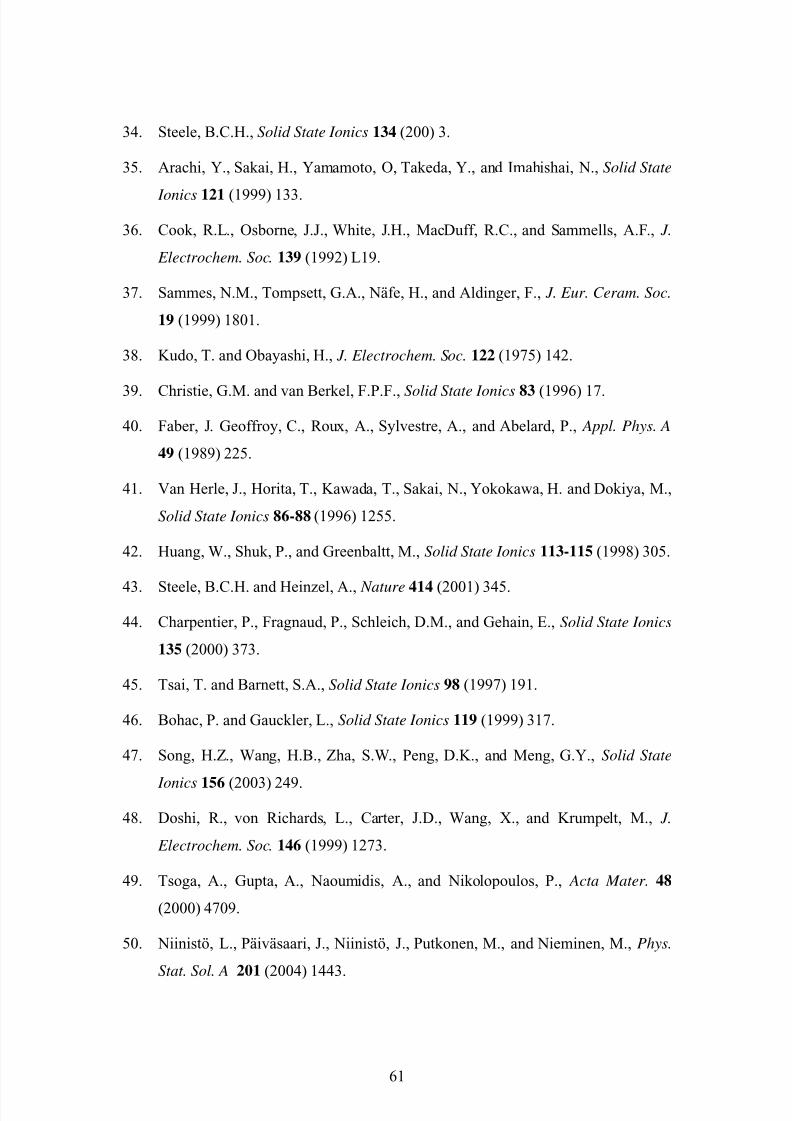
5/13/2018 ALD of Lanthanide Oxide Thin Films - slidepdf.com
http://slidepdf.com/reader/full/ald-of-lanthanide-oxide-thin-films 61/6961
34. Steele, B.C.H., Solid State Ionics 134 (200) 3.
35. Arachi, Y., Sakai, H., Yamamoto, O, Takeda, Y., and Imahishai, N., Solid State
Ionics 121 (1999) 133.
36. Cook, R.L., Osborne, J.J., White, J.H., MacDuff, R.C., and Sammells, A.F., J.
Electrochem. Soc. 139 (1992) L19.
37. Sammes, N.M., Tompsett, G.A., Näfe, H., and Aldinger, F., J. Eur. Ceram. Soc.
19 (1999) 1801.
38. Kudo, T. and Obayashi, H., J. Electrochem. Soc. 122 (1975) 142.
39. Christie, G.M. and van Berkel, F.P.F., Solid State Ionics 83 (1996) 17.
40. Faber, J. Geoffroy, C., Roux, A., Sylvestre, A., and Abelard, P., Appl. Phys. A
49 (1989) 225.
41. Van Herle, J., Horita, T., Kawada, T., Sakai, N., Yokokawa, H. and Dokiya, M.,
Solid State Ionics 86-88 (1996) 1255.
42. Huang, W., Shuk, P., and Greenbaltt, M., Solid State Ionics 113-115 (1998) 305.
43. Steele, B.C.H. and Heinzel, A., Nature 414 (2001) 345.
44. Charpentier, P., Fragnaud, P., Schleich, D.M., and Gehain, E., Solid State Ionics
135 (2000) 373.
45. Tsai, T. and Barnett, S.A., Solid State Ionics 98 (1997) 191.
46. Bohac, P. and Gauckler, L., Solid State Ionics 119 (1999) 317.
47. Song, H.Z., Wang, H.B., Zha, S.W., Peng, D.K., and Meng, G.Y., Solid State
Ionics 156 (2003) 249.
48. Doshi, R., von Richards, L., Carter, J.D., Wang, X., and Krumpelt, M., J.
Electrochem. Soc. 146 (1999) 1273.
49. Tsoga, A., Gupta, A., Naoumidis, A., and Nikolopoulos, P., Acta Mater. 48
(2000) 4709.
50. Niinistö, L., Päiväsaari, J., Niinistö, J., Putkonen, M., and Nieminen, M., Phys.
Stat. Sol. A 201 (2004) 1443.
5/13/2018 ALD of Lanthanide Oxide Thin Films - slidepdf.com
http://slidepdf.com/reader/full/ald-of-lanthanide-oxide-thin-films 62/6962
51. Niinistö, L., Ritala, M., and Leskelä, M., Mater. Sci. Eng. B 41 (1996) 23.
52. Putkonen, M., Development of Low-temperature Deposition Processes by
Atomic Layer Epitaxy for Binary and Ternary Oxide Thin Films, Ph.D. Thesis,Helsinki University of Technology, Helsinki 2002, 69 p.
53. Rahtu, A., Atomic Layer Deposition of High Permittivity Oxides: Film Growth
and In Situ Studies, Ph. D. Thesis, University of Helsinki, Helsinki 2002, 69 p.
54. Niinistö, J., Rahtu, A., Putkonen, M., Ritala, M., Leskelä, M., and Niinistö, L.,
Langmuir 21 (2005) 7321-7325.
55. Liu, X., Ramanathan, S., Longdergan, A., Srivastava, A., Lee, E., Seidel, T.E.,
Barton, J.T., Pang, D., and Gordon, R.G., J. Electrochem. Soc. 152 (2005)
G213.
56. Kim, S.K., Hwang, C.S., Park, S.-H.K., and Yun, S.J., Thin Solid Films 478
(2005) 103.
57. Puurunen, R.L., Chem. Vap. Deposition 9 (2003) 327.
58. Suntola, T., In: Handbook of Thin Film Process Technology (Ed. D.A. Glocker),
IOP Publishing Ltd, London 1995, pp. B1.5:1-17.
59. Ritala, M., Leskelä, M., Dekker, J.-P., Mutsaers, C., Soininen, P.J., and Skarp,
J., Chem. Vap. Deposition 5 (1999) 7.
60. Ohmi, S., Takeda, M., Ishiwara, H., and Iwai, H., J. Electrochem. Soc. 151
(2004) G279.
61. Ohmi, S., Kobayashi, C., Kashiwagi, I., Ohsima, C., Ishiwara, H., and Iwai, H.,
J. Electrochem. Soc. 150 (2004) F134.
62. Landheer, D., Gupta, J.A., Sproule, G.I., McCaffrey, J.P., Graham, M.J., Yang,
K.-C., Lu, Z.-H., and Lennard, W.N., J. Electrochem. Soc. 148 (2001) G29.
63. Mikhelasvili, V., Eisenstein, G., Edelman, F., Brener, R., Zakharov, N., and
Werner, P., J. Appl. Phys. 95 (2004) 613.
5/13/2018 ALD of Lanthanide Oxide Thin Films - slidepdf.com
http://slidepdf.com/reader/full/ald-of-lanthanide-oxide-thin-films 63/6963
64. Jeon, S., Im, K:, Yang, H., Lee, H., Sim, H., Choi, S., Jang, T., and Hwang, H.,
Proc. International Electron Devices Meeting 2001, IEDM Technical Digest
(2001) 20.6.1.
65. Wiktorczyk, T., J. Electrostat. 51-52 (2001) 131.
66. Li, Y.-L., Chen, N.-F., Zhou, J.-P., Song, S.-L., Liu, L.-F., Yin, Z.-G., and Cai,
C.-L., J. Cryst. Growth 265 (2004) 548.
67. Ono, H. and Katsumata, T., Appl. Phys. Lett. 78 (2001) 1832.
68. Shiokawa, Y., Amano, R., Nomura, A., and Yagi, M., J. Radioanal. Nucl.
Chem. 152 (1991) 373.
69. Becht, M., Gerfin, T., and Dahmen, K.-H., Chem. Mater. 5 (1993) 137.
70. Sharma, R.N. and Rastogi, A.C., J. Appl. Phys. 74 (1993) 6691.
71. Bonnet, G., Lachkar, M., Larpin, J.P., and Corson, J.C., Solid-State Ionics 72
(1994) 344.
72. Tasaki, Y., Satoh, M., Yoshizawa, S., Kataoka, H., and Hidaka, H., Jpn. J. Appl.
Phys. 36 (1997) 6871.
73. Lo Nigro, R., Toro, R.G., Malandrino, G., Raineri, V., and Fragalà, I.L., Adv.
Mater. 15 (2003) 1071.
74. Cheng, J.-B., Li, A.-D., Shao, Q.Y., Ling, H.-Q., Wu, D., Wang, Y., Bao, Y.-J.,
Wang, M., Liu, Z.-G., and Ming, N.-B., Appl. Surf. Sci. 233 (2004) 91.
75. Lo Nigro, R., Toro, R.G., Malandrino, G., Raineri, V., and Fragalà, I.L., Mater.
Sci. Eng. B 118 (2005) 117.
76. Weber, A. and Suhr, H., Mod. Phys. Lett. 3 (1989) 1001.
77. Song, M.-K. and Rhee, S.-W., Thin Solid Films 492 (2005) 19.
78. Fleeting, K.A., Davies, H.O., Jones, A.C., O’Brien, P., Leedham, T.J., Crosbie,
M.J., Wright, P.J., and Williams, D.J., Chem. Vap. Deposition 5 (1999) 261.
79. Kang, S.-W. and Rhee, S.-W., J. Electrochem. Soc. 149 (2002) C345.
5/13/2018 ALD of Lanthanide Oxide Thin Films - slidepdf.com
http://slidepdf.com/reader/full/ald-of-lanthanide-oxide-thin-films 64/6964
80. McAleese, J., Plakatouras, J.C, and Steele, B.C.H., Thin Solid Films 286 (1996)
64.
81. Singh, M.P., Shalini, K., and Shivashankar, S.A., Proc. Electrochem. Soc. 2003-
08 (2003) 821.
82. Singh, M.P. and Shivashankar, S.A., J. Cryst. Growth 276 (2005) 148.
83. Aspinall, H.C., Gaskell, J., Williams, P.A., Jones, A.C., Chalker, P.R., Marshall,
P.A., Smith, L.M., and Critchlow, G.W., Chem. Vap. Deposition 10 (2004) 13.
84. Aspinall, H.C., Gaskell, J., Williams, P.A., Jones, A.C., Chalker, P.R., Marshall,
P.A., Bickley, J.F., Smith, L.M., and Critchlow, G.W., Chem. Vap. Deposition 9
(2003) 235.
85. Aspinall, H.C., Gaskell, J., Williams, P.A., Jones, A.C., Chalker, P.R., Marshall,
P.A., Smith, L.M., and Critchlow, G.W., Chem. Vap. Deposition 10 (2004) 83.
86. Loo, Y.F., Potter, R.J., Jones, A.C., Aspinall, H.C., Gaskell, J., Chalker, P.R.,
Smith, L.M., and Critchlow, G.W., Chem. Vap. Deposition 10 (2004) 306.
87. Aspinall, H.C., Gaskell, J., Loo, Y.F., Jones, A.C., Chalker, P.R., Potter, R.J.,
Smith, L.M., and Critchlow, G.W., Chem. Vap. Deposition 10 (2004) 301.
88. Päiväsaari, J., Niinistö, J., Myllymäki, P., Dezelah, C., Putkonen, M., Nieminen,
M., and Niinistö, L., Topics Appl. Phys. (2006) In press.
89. Putkonen, M., Nieminen, M., Niinistö, J., Sajavaara, T., and Niinistö, L.,Chem.
Mater. 13 (2001) 4701.
90. Putkonen, M., Sajavaara, T., Johansson, L.-S., and Niinistö, L., Chem. Vap.
Deposition 7 (2001) 44.
91. Gusev, E.P., Cartier, E., Buchanan, D.A., Gribelyuk, M., Copel, M., Okorn-
Schmidt, H., and D’Emic, C., Microelectron. Eng. 59 (2001) 341.
92. Mölsä, H., Niinistö, L., and Utriainen, M., Adv. Mater. Opt. Electron. 4 (1994)
389.
93. Nieminen, M., Putkonen, M., and Niinistö, L., Appl. Surf. Sci. 174 (2001) 155.
94. Mölsä, H. and Niinistö, L., Mater. Res. Soc. Symp. Proc. 355 (1994) 341.
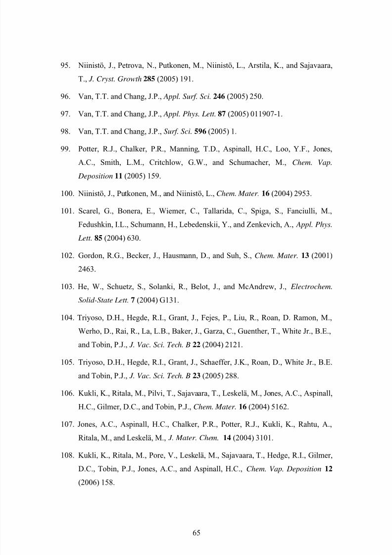
5/13/2018 ALD of Lanthanide Oxide Thin Films - slidepdf.com
http://slidepdf.com/reader/full/ald-of-lanthanide-oxide-thin-films 65/6965
95. Niinistö, J., Petrova, N., Putkonen, M., Niinistö, L., Arstila, K., and Sajavaara,
T., J. Cryst. Growth 285 (2005) 191.
96. Van, T.T. and Chang, J.P., Appl. Surf. Sci. 246 (2005) 250.
97. Van, T.T. and Chang, J.P., Appl. Phys. Lett. 87 (2005) 011907-1.
98. Van, T.T. and Chang, J.P., Surf. Sci. 596 (2005) 1.
99. Potter, R.J., Chalker, P.R., Manning, T.D., Aspinall, H.C., Loo, Y.F., Jones,
A.C., Smith, L.M., Critchlow, G.W., and Schumacher, M., Chem. Vap.
Deposition 11 (2005) 159.
100. Niinistö, J., Putkonen, M., and Niinistö, L.,Chem. Mater. 16 (2004) 2953.
101. Scarel, G., Bonera, E., Wiemer, C., Tallarida, C., Spiga, S., Fanciulli, M.,
Fedushkin, I.L., Schumann, H., Lebedenskii, Y., and Zenkevich, A., Appl. Phys.
Lett. 85 (2004) 630.
102. Gordon, R.G., Becker, J., Hausmann, D., and Suh, S., Chem. Mater. 13 (2001)
2463.
103. He, W., Schuetz, S., Solanki, R., Belot, J., and McAndrew, J., Electrochem.
Solid-State Lett. 7 (2004) G131.
104. Triyoso, D.H., Hegde, R.I., Grant, J., Fejes, P., Liu, R., Roan, D. Ramon, M.,
Werho, D., Rai, R., La, L.B., Baker, J., Garza, C., Guenther, T., White Jr., B.E.,
and Tobin, P.J., J. Vac. Sci. Tech. B 22 (2004) 2121.
105. Triyoso, D.H., Hegde, R.I., Grant, J., Schaeffer, J.K., Roan, D., White Jr., B.E.
and Tobin, P.J., J. Vac. Sci. Tech. B 23 (2005) 288.
106. Kukli, K., Ritala, M., Pilvi, T., Sajavaara, T., Leskelä, M., Jones, A.C., Aspinall,
H.C., Gilmer, D.C., and Tobin, P.J., Chem. Mater. 16 (2004) 5162.
107. Jones, A.C., Aspinall, H.C., Chalker, P.R., Potter, R.J., Kukli, K., Rahtu, A.,
Ritala, M., and Leskelä, M., J. Mater. Chem. 14 (2004) 3101.
108. Kukli, K., Ritala, M., Pore, V., Leskelä, M., Sajavaara, T., Hedge, R.I., Gilmer,
D.C., Tobin, P.J., Jones, A.C., and Aspinall, H.C., Chem. Vap. Deposition 12
(2006) 158.
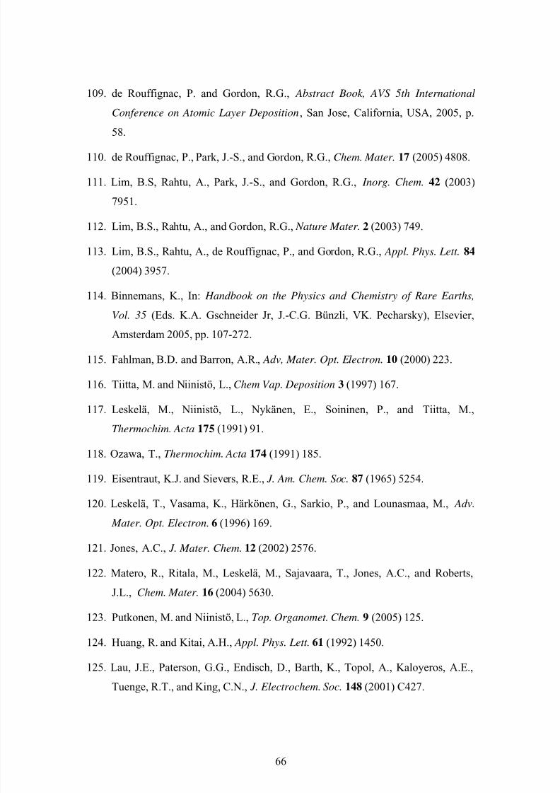
5/13/2018 ALD of Lanthanide Oxide Thin Films - slidepdf.com
http://slidepdf.com/reader/full/ald-of-lanthanide-oxide-thin-films 66/6966
109. de Rouffignac, P. and Gordon, R.G., Abstract Book, AVS 5th International
Conference on Atomic Layer Deposition, San Jose, California, USA, 2005, p.
58.
110. de Rouffignac, P., Park, J.-S., and Gordon, R.G., Chem. Mater. 17 (2005) 4808.
111. Lim, B.S, Rahtu, A., Park, J.-S., and Gordon, R.G., Inorg. Chem. 42 (2003)
7951.
112. Lim, B.S., Rahtu, A., and Gordon, R.G., Nature Mater. 2 (2003) 749.
113. Lim, B.S., Rahtu, A., de Rouffignac, P., and Gordon, R.G., Appl. Phys. Lett. 84
(2004) 3957.
114. Binnemans, K., In: Handbook on the Physics and Chemistry of Rare Earths,
Vol. 35 (Eds. K.A. Gschneider Jr, J.-C.G. Bünzli, VK. Pecharsky), Elsevier,
Amsterdam 2005, pp. 107-272.
115. Fahlman, B.D. and Barron, A.R., Adv, Mater. Opt. Electron. 10 (2000) 223.
116. Tiitta, M. and Niinistö, L.,Chem Vap. Deposition 3 (1997) 167.
117. Leskelä, M., Niinistö, L., Nykänen, E., Soininen, P., and Tiitta, M.,
Thermochim. Acta 175 (1991) 91.
118. Ozawa, T., Thermochim. Acta 174 (1991) 185.
119. Eisentraut, K.J. and Sievers, R.E., J. Am. Chem. Soc. 87 (1965) 5254.
120. Leskelä, T., Vasama, K., Härkönen, G., Sarkio, P., and Lounasmaa, M., Adv.
Mater. Opt. Electron. 6 (1996) 169.
121. Jones, A.C., J. Mater. Chem. 12 (2002) 2576.
122. Matero, R., Ritala, M., Leskelä, M., Sajavaara, T., Jones, A.C., and Roberts,
J.L., Chem. Mater. 16 (2004) 5630.
123. Putkonen, M. and Niinistö, L., Top. Organomet. Chem. 9 (2005) 125.
124. Huang, R. and Kitai, A.H., Appl. Phys. Lett. 61 (1992) 1450.
125. Lau, J.E., Paterson, G.G., Endisch, D., Barth, K., Topol, A., Kaloyeros, A.E.,
Tuenge, R.T., and King, C.N., J. Electrochem. Soc. 148 (2001) C427.
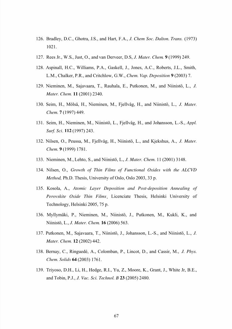
5/13/2018 ALD of Lanthanide Oxide Thin Films - slidepdf.com
http://slidepdf.com/reader/full/ald-of-lanthanide-oxide-thin-films 67/6967
126. Bradley, D.C., Ghotra, J.S., and Hart, F.A., J. Chem Soc. Dalton. Trans. (1973)
1021.
127. Rees Jr., W.S., Just, O., and van Derveer, D.S, J. Mater. Chem. 9 (1999) 249.
128. Aspinall, H.C., Williams, P.A., Gaskell, J., Jones, A.C., Roberts, J.L., Smith,
L.M., Chalker, P.R., and Critchlow, G.W., Chem. Vap. Deposition 9 (2003) 7.
129. Nieminen, M., Sajavaara, T., Rauhala, E., Putkonen, M., and Niinistö, L., J.
Mater. Chem. 11 (2001) 2340.
130. Seim, H., Mölsä, H., Nieminen, M., Fjellvåg, H., and Niinistö, L., J. Mater.
Chem. 7 (1997) 449.
131. Seim, H., Nieminen, M., Niinistö, L., Fjellvåg, H., and Johansson, L.-S., Appl.
Surf. Sci. 112 (1997) 243.
132. Nilsen, O., Peussa, M., Fjellvåg, H., Niinistö, L., and Kjekshus, A., J. Mater.
Chem. 9 (1999) 1781.
133. Nieminen, M., Lehto, S., and Niinistö, L., J. Mater. Chem. 11 (2001) 3148.
134. Nilsen, O., Growth of Thin Films of Functional Oxides with the ALCVD
Method, Ph.D. Thesis, University of Oslo, Oslo 2003, 33 p.
135. Kosola, A., Atomic Layer Deposition and Post-deposition Annealing of
Perovskite Oxide Thin Films¸ Licenciate Thesis, Helsinki University of
Technology, Helsinki 2005, 75 p.
136. Myllymäki, P., Nieminen, M., Niinistö, J., Putkonen, M., Kukli, K., and
Niinistö, L., J. Mater. Chem. 16 (2006) 563.
137. Putkonen, M., Sajavaara, T., Niinistö, J., Johansson, L.-S., and Niinistö, L., J.
Mater. Chem. 12 (2002) 442.
138. Bernay, C., Ringuedé, A., Colomban, P., Lincot, D., and Cassir, M., J. Phys.
Chem. Solids 64 (2003) 1761.
139. Triyoso, D.H., Li, H., Hedge, R.I., Yu, Z., Moore, K., Grant, J., White Jr, B.E.,
and Tobin, P.J., J. Vac. Sci. Technol. B 23 (2005) 2480.
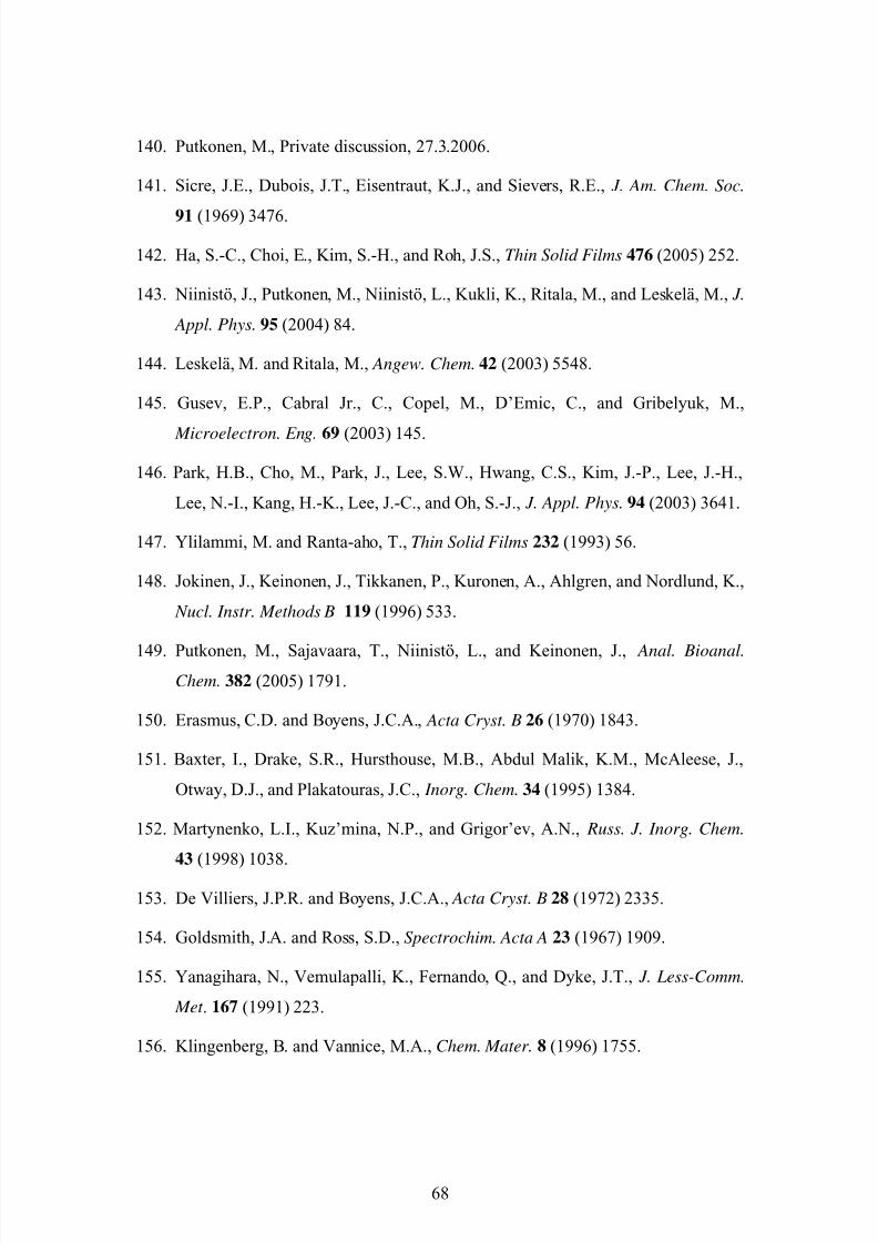
5/13/2018 ALD of Lanthanide Oxide Thin Films - slidepdf.com
http://slidepdf.com/reader/full/ald-of-lanthanide-oxide-thin-films 68/6968
140. Putkonen, M., Private discussion, 27.3.2006.
141. Sicre, J.E., Dubois, J.T., Eisentraut, K.J., and Sievers, R.E., J. Am. Chem. Soc.
91 (1969) 3476.
142. Ha, S.-C., Choi, E., Kim, S.-H., and Roh, J.S., Thin Solid Films 476 (2005) 252.
143. Niinistö, J., Putkonen, M., Niinistö, L., Kukli, K., Ritala, M., and Leskelä, M., J.
Appl. Phys. 95 (2004) 84.
144. Leskelä, M. and Ritala, M., Angew. Chem. 42 (2003) 5548.
145. Gusev, E.P., Cabral Jr., C., Copel, M., D’Emic, C., and Gribelyuk, M.,
Microelectron. Eng. 69 (2003) 145.
146. Park, H.B., Cho, M., Park, J., Lee, S.W., Hwang, C.S., Kim, J.-P., Lee, J.-H.,
Lee, N.-I., Kang, H.-K., Lee, J.-C., and Oh, S.-J., J. Appl. Phys. 94 (2003) 3641.
147. Ylilammi, M. and Ranta-aho, T., Thin Solid Films 232 (1993) 56.
148. Jokinen, J., Keinonen, J., Tikkanen, P., Kuronen, A., Ahlgren, and Nordlund, K.,
Nucl. Instr. Methods B 119 (1996) 533.
149. Putkonen, M., Sajavaara, T., Niinistö, L., and Keinonen, J., Anal. Bioanal.
Chem. 382 (2005) 1791.
150. Erasmus, C.D. and Boyens, J.C.A., Acta Cryst. B 26 (1970) 1843.
151. Baxter, I., Drake, S.R., Hursthouse, M.B., Abdul Malik, K.M., McAleese, J.,
Otway, D.J., and Plakatouras, J.C., Inorg. Chem. 34 (1995) 1384.
152. Martynenko, L.I., Kuz’mina, N.P., and Grigor’ev, A.N., Russ. J. Inorg. Chem.
43 (1998) 1038.
153. De Villiers, J.P.R. and Boyens, J.C.A., Acta Cryst. B 28 (1972) 2335.
154. Goldsmith, J.A. and Ross, S.D., Spectrochim. Acta A 23 (1967) 1909.
155. Yanagihara, N., Vemulapalli, K., Fernando, Q., and Dyke, J.T., J. Less-Comm.
Met . 167 (1991) 223.
156. Klingenberg, B. and Vannice, M.A., Chem. Mater. 8 (1996) 1755.
5/13/2018 ALD of Lanthanide Oxide Thin Films - slidepdf.com
http://slidepdf.com/reader/full/ald-of-lanthanide-oxide-thin-films 69/6969
157. Leskelä, M. and Niinistö, L., In: Handbook on the Physics and Chemistry of
Rare Earths, Vol. 8, Elsevier, Amsterdam 1986, pp. 203-334.
158. Kwo, J., Hong, M., Kortan, A.R., Queeney, K.T., Chabal, Y.J., Mannaerts, J.P.,
Boone, T., Krajewski, J.J., Sergent, A.M., and Rosamilia, J.M., Appl. Phys. Lett.
77 (2000) 130.
159. Zhou, J.-P., Chai, C.-L., Yang, S.-Y., Liu, Z.-K., Song, S.-L., Li, Y.-L., and
Chen, N.-F., J. Cryst. Growth 270 (2004) 21.
160. Song, H.Z., Wang, H.B., Zhang, J., Peng, D.K., and Meng, G.Y., Mater. Res.
Bull. 37 (2002) 1487.