chapter 6. converter circuits - uic engineeringvahe/fall2002/ece445/pdf/ch6slide.pdf ·...
TRANSCRIPT

Fundamentals of Power Electronics Chapter 6: Converter circuits1
Chapter 6. Converter Circuits
6.1. Circuit manipulations
6.2. A short list of converters
6.3. Transformer isolation
6.4. Converter evaluation and design
6.5. Summary of key points
• Where do the boost, buck-boost, and other converters originate?
• How can we obtain a converter having given desired properties?
• What converters are possible?
• How can we obtain transformer isolation in a converter?
• For a given application, which converter is best?

Fundamentals of Power Electronics Chapter 6: Converter circuits2
6.1. Circuit manipulations
+–Vg
L
C R
+
V
–
1
2
Begin with buck converter: derived in chapter 1 from first principles
• Switch changes dc component, low-pass filter removes switching harmonics
• Conversion ratio is M = D

Fundamentals of Power Electronics Chapter 6: Converter circuits3
6.1.1. Inversion of source and load
Interchange power input and output ports of a converter
Buck converter example
port 1 port 2
+–
L1
2+
V1
–
+
V2
–
Power flow
V2 = DV1

Fundamentals of Power Electronics Chapter 6: Converter circuits4
Inversion of source and load
port 1 port 2
+–
L1
2+
V1
–
+
V2
–
Power flow
Interchange power source and load:
V2 = DV1 V1 = 1D V2
Fundamentals of Power Electronics Chapter 6: Converter circuits5
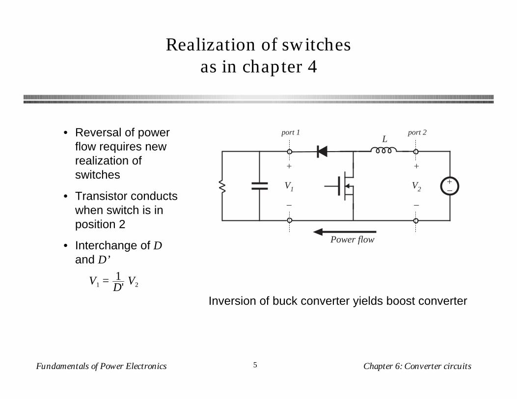
Realization of switchesas in chapter 4
V1 = 1D'
V2
port 1 port 2
+–
L
+
V1
–
+
V2
–
Power flow
• Reversal of power flow requires new realization of switches
• Transistor conducts when switch is in position 2
• Interchange of D and D’
Inversion of buck converter yields boost converter

Fundamentals of Power Electronics Chapter 6: Converter circuits6
6.1.2. Cascade connection of converters
+–
converter 2converter 1
Vg
+
V1
–
+
V
–
D
V1
Vg= M 1(D)
VV1
= M 2(D)
V1 = M 1(D) Vg
V = M 2(D) V1
VVg
= M(D) = M 1(D) M 2(D)
Fundamentals of Power Electronics Chapter 6: Converter circuits7
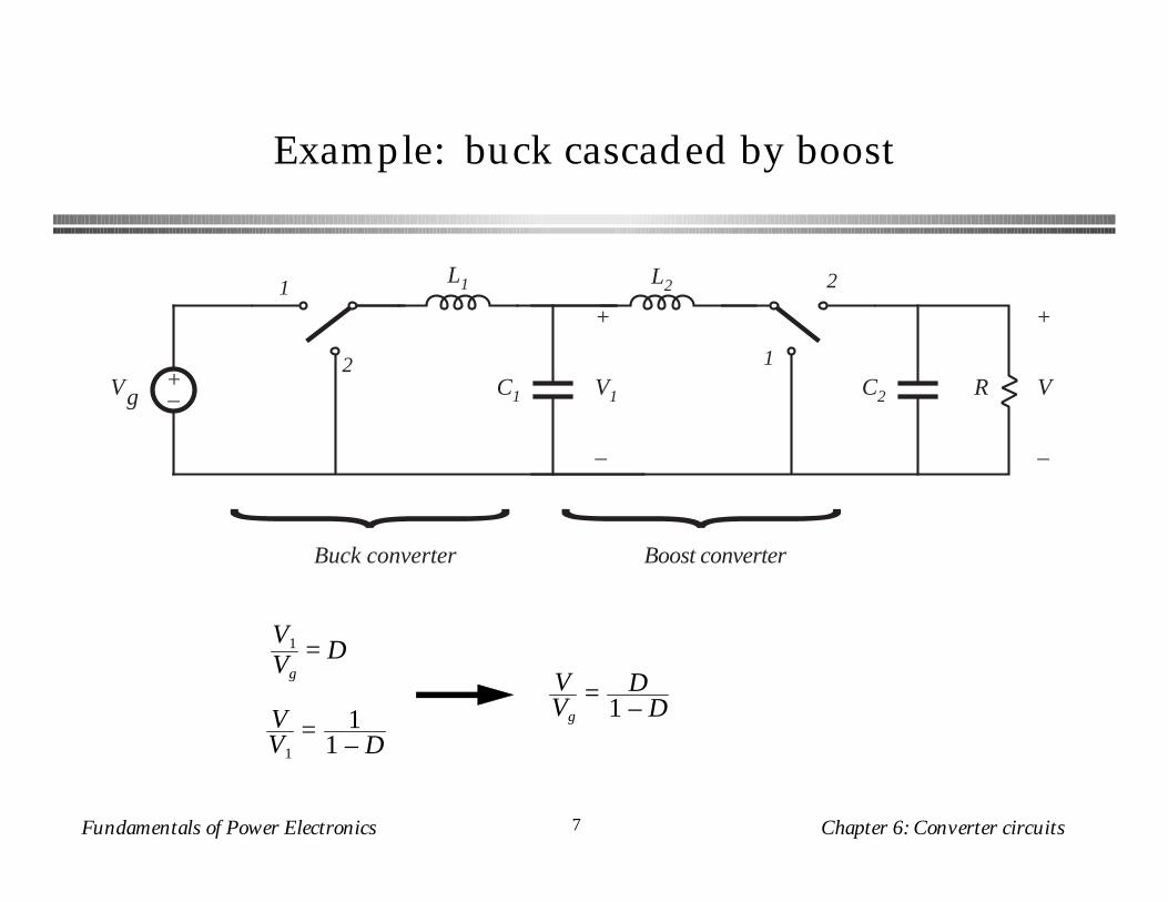
Example: buck cascaded by boost
+–Vg
1
2
L1
C1
+
V1
–
R
+
V
–
1
2L2
C2{ {Buck converter Boost converter
V1
Vg= D
VV1
= 11 – D
VVg
= D1 – D

Fundamentals of Power Electronics Chapter 6: Converter circuits8
Buck cascaded by boost:simplification of internal filter
+–Vg
1
2
L1
R
+
V
–
1
2L2
C2
+
V
–
1
2L
+–Vg
1
2
iL
remove capacitor C1
combine inductors L1 and L2
Noninverting buck-boost converter

Fundamentals of Power Electronics Chapter 6: Converter circuits9
Noninverting buck-boost converter
+
V
–
1
2L
+–Vg
1
2
iL
+–
+
V
–
Vg
iL
+–
+
V
–
Vg
iL
subinterval 1 subinterval 2

Fundamentals of Power Electronics Chapter 6: Converter circuits10
Reversal of output voltage polarity
+–
+
V
–
Vg
iL
+–
+
V
–
Vg
iL
+–
+
V
–
Vg
iL
+–
+
V
–
Vg
iL
subinterval 1 subinterval 2
noninverting buck-boost
inverting buck-boost

Fundamentals of Power Electronics Chapter 6: Converter circuits11
Reduction of number of switches:inverting buck-boost
+–
+
V
–
Vg
iL
+–
+
V
–
Vg
iL
subinterval 1 subinterval 2
One side of inductor always connected to ground— hence, only one SPDT switch needed:
+–
+
V
–
1 2
Vg
iL VVg
= – D1 – D

Fundamentals of Power Electronics Chapter 6: Converter circuits12
Discussion: cascade connections
• Properties of buck-boost converter follow from its derivation as buck cascaded by boost
Equivalent circuit model: buck 1:D transformer cascaded by boost D’:1 transformer
Pulsating input current of buck converter
Pulsating output current of boost converter
• Other cascade connections are possible
Cuk converter: boost cascaded by buck

Fundamentals of Power Electronics Chapter 6: Converter circuits13
6.1.3. Rotation of three-terminal cell
+–
+
v
–
1
2Vg
three-terminal cell
aA b B
c
C
Treat inductor and SPDT switch as three-terminal cell:
Three-terminal cell can be connected between source and load in three nontrivial distinct ways:
a-A b-B c-C buck converter
a-C b-A c-B boost converter
a-A b-C c-B buck-boost converter
Fundamentals of Power Electronics Chapter 6: Converter circuits14
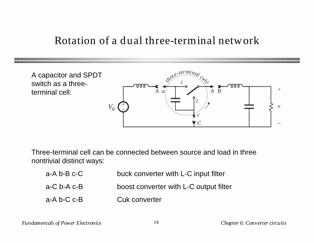
Rotation of a dual three-terminal network
+–Vg
+
v
–
1
2
th
ree-terminal cel l
A a b B
c
C
A capacitor and SPDT switch as a three-terminal cell:
Three-terminal cell can be connected between source and load in three nontrivial distinct ways:
a-A b-B c-C buck converter with L-C input filter
a-C b-A c-B boost converter with L-C output filter
a-A b-C c-B Cuk converter

Fundamentals of Power Electronics Chapter 6: Converter circuits15
6.1.4. Differential connection of loadto obtain bipolar output voltage
converter 1 +
V1
–+
V
–D
converter 2
+–Vg
+
V2
–
D'
loaddc source
V1 = M(D) Vg
V2 = M(D') Vg
Differential load voltage is
V = V1 – V2
The outputs V1 and V2 may both be positive, but the differential output voltage V can be positive or negative.

Fundamentals of Power Electronics Chapter 6: Converter circuits16
Differential connection using two buck converters
+
V1
–+
V
–+–Vg
+
V2
–
1
2
1
2
Buck converter 1}Buck converter 2
{Converter #1 transistor driven with duty cycle D
Converter #2 transistor driven with duty cycle complement D’
Differential load voltage is
V = DVg – D'Vg
V = (2D – 1) Vg
Simplify:

Fundamentals of Power Electronics Chapter 6: Converter circuits17
Conversion ratio M(D),differentially-connected buck converters
V = (2D – 1) Vg
D
M(D)
10.5
1
0
– 1

Fundamentals of Power Electronics Chapter 6: Converter circuits18
Simplification of filter circuit,differentially-connected buck converters
+–Vg
1
2
1
2
+
V
–
+
V1
–+
V
–+–Vg
+
V2
–
1
2
1
2
Buck converter 1}
Buck converter 2
{Original circuit Bypass load directly with capacitor
Fundamentals of Power Electronics Chapter 6: Converter circuits19
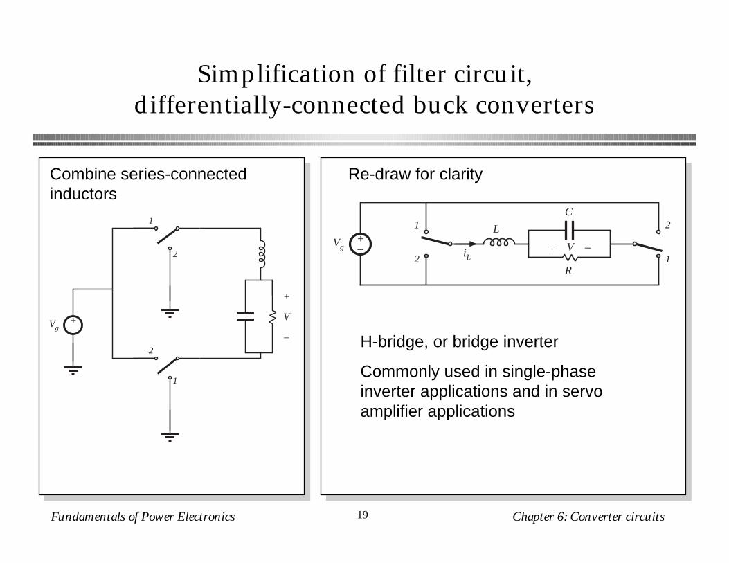
Simplification of filter circuit,differentially-connected buck converters
Combine series-connected inductors
Re-draw for clarity
+–Vg
1
2
1
2
+
V
–
+–
L
C
R
+ V –
2
1iL
Vg
1
2
H-bridge, or bridge inverter
Commonly used in single-phase inverter applications and in servo amplifier applications

Fundamentals of Power Electronics Chapter 6: Converter circuits20
Differential connection to obtain 3ø inverter
converter 1 +
V1
–
converter 2
+–Vg
+
V2
–
3øac loaddc source
converter 3 +
V3
–
D1
D2
D3
Vn+ vbn –
– v an
+
– vcn +
V1 = M(D1) Vg
V2 = M(D2) Vg
V3 = M(D3) Vg
With balanced 3ø load, neutral voltage is
Vn = 13
(V1 + V2 + V3)
Van = V1 – Vn
Vbn = V2 – Vn
Vcn = V3 – Vn
Phase voltages are
Control converters such that their output voltages contain the same dc biases. This dc bias will appear at the neutral point Vn. It then cancels out, so phase voltages contain no dc bias.

Fundamentals of Power Electronics Chapter 6: Converter circuits21
3ø differential connection of three buck converters
+
V1
–
+–Vg
+
V2
–
3øac loaddc source
+
V3
–
Vn+ vbn –
– v an
+
– vcn +

Fundamentals of Power Electronics Chapter 6: Converter circuits22
3ø differential connection of three buck converters
3øac loaddc source
Vn+ vbn –
– v an
+
– vcn +
+–Vg
Re-draw for clarity:
“Voltage-source inverter” or buck-derived three-phase inverter
Fundamentals of Power Electronics Chapter 6: Converter circuits23
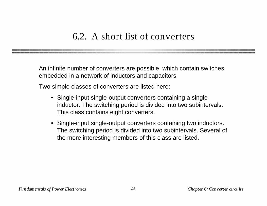
6.2. A short list of converters
An infinite number of converters are possible, which contain switches embedded in a network of inductors and capacitors
Two simple classes of converters are listed here:
• Single-input single-output converters containing a single inductor. The switching period is divided into two subintervals. This class contains eight converters.
• Single-input single-output converters containing two inductors. The switching period is divided into two subintervals. Several of the more interesting members of this class are listed.

Fundamentals of Power Electronics Chapter 6: Converter circuits24
Single-input single-output converterscontaining one inductor
• Use switches to connect inductor between source and load, in one manner during first subinterval and in another during second subinterval
• There are a limited number of ways to do this, so all possible combinations can be found
• After elimination of degenerate and redundant cases, eight converters are found:
dc-dc converters
buck boost buck-boost noninverting buck-boost
dc-ac converters
bridge Watkins-Johnson
ac-dc converters
current-fed bridge inverse of Watkins-Johnson

Fundamentals of Power Electronics Chapter 6: Converter circuits25
Converters producing a unipolar output voltage
2. Boost
+–
+
V
–
1
2
Vg
M(D) = 11 – D
1. Buck
+–
+
V
–
1
2Vg
M(D) = DM(D)
D
1
0
0.5
0 0.5 1
M(D)
D
2
0
1
0 0.5 1
3
4

Fundamentals of Power Electronics Chapter 6: Converter circuits26
Converters producing a unipolar output voltage
+–
+
V
–
1 2
Vg
3. Buck-boost M(D) = – D1 – D
+
V
–
1
2
+–
1
2Vg
4. Noninverting buck-boost M(D) = D1 – D
M(D)
–3
0
–4
–2
–1
D0 0.5 1
M(D)
D
2
0
1
0 0.5 1
3
4

Fundamentals of Power Electronics Chapter 6: Converter circuits27
Converters producing a bipolar output voltagesuitable as dc-ac inverters
6. Watkins-Johnson
5. Bridge M(D) = 2D – 1
M(D) = 2D – 1D
1
2
+– + V –Vg
2
1
M(D)
1
–1
0D0.5 1
+–
12
1 2
Vg
+
V
–
M(D)
D0.5 1–1
–3
–2
0
1
+
V
–
+–
1
2Vg
or

Fundamentals of Power Electronics Chapter 6: Converter circuits28
Converters producing a bipolar output voltagesuitable as ac-dc rectifiers
7. Current-fed bridge
8. Inverse of Watkins-Johnson
M(D) = 12D – 1
M(D) = D2D – 1
M(D)
–1
2
–2
0
1D0.5 1
M(D)
–1
2
–2
0
1D0.5 1
+– + V –
1
2
2
1
Vg
+–Vg
21
2 1
+
V
–
or+
V
–
+–Vg
1
2

Fundamentals of Power Electronics Chapter 6: Converter circuits29
Several members of the class of two-inductor converters
2. SEPIC
1. Cuk M(D) = – D1 – D
M(D) = D1 – D
M(D)
–3
0
–4
–2
–1
D0 0.5 1
M(D)
D
2
0
1
0 0.5 1
3
4
+–
+
V
–
1 2Vg
+–
+
V
–
Vg 1
2

Fundamentals of Power Electronics Chapter 6: Converter circuits30
Several members of the class of two-inductor converters
3. Inverse of SEPIC
4. Buck 2 M(D) = D2
M(D) = D1 – D
M(D)
D
2
0
1
0 0.5 1
3
4
M(D)
D
1
0
0.5
0 0.5 1
+–
1
2Vg
+
V
–
+–Vg
1
2
1
2
+
V
–

Fundamentals of Power Electronics Chapter 6: Converter circuits31
6.3. Transformer isolation
Objectives:
• Isolation of input and output ground connections, to meet safety requirements
• Reduction of transformer size by incorporating high frequency isolation transformer inside converter
• Minimization of current and voltage stresses when a large step-up or step-down conversion ratio is needed —use transformer turns ratio
• Obtain multiple output voltages via multiple transformer secondary windings and multiple converter secondary circuits

Fundamentals of Power Electronics Chapter 6: Converter circuits32
A simple transformer model
n1 : n2
: n3
+
v1(t)
–
+
v2(t)
–
+
v3(t)
–
i1(t) i2(t)
i3(t)
n1 : n2
: n3
+
v1(t)
–
+
v2(t)
–
+
v3(t)
–
i1(t) i2(t)
i3(t)
idealtransformer
i1'(t)
LM
iM(t)
Multiple winding transformer Equivalent circuit model
v1(t)n1
=v2(t)n2
=v3(t)n3
= ...
0 = n1i1'(t) + n2i2(t) + n3i3(t) + ...

Fundamentals of Power Electronics Chapter 6: Converter circuits33
The magnetizing inductance LM
B(t) ∝ v1(t) dt
H(t) ∝ iM(t)
slope ∝ LM
saturation
Transformer core B-H characteristic• Models magnetization of transformer core material
• Appears effectively in parallel with windings
• If all secondary windings are disconnected, then primary winding behaves as an inductor, equal to the magnetizing inductance
• At dc: magnetizing inductance tends to short-circuit. Transformers cannot pass dc voltages
• Transformer saturates when magnetizing current iM is too large

Fundamentals of Power Electronics Chapter 6: Converter circuits34
Volt-second balance in LM
n1 : n2
: n3
+
v1(t)
–
+
v2(t)
–
+
v3(t)
–
i1(t) i2(t)
i3(t)
idealtransformer
i1'(t)
LM
iM(t)
The magnetizing inductance is a real inductor, obeying
v1(t) = LM
diM(t)dt
integrate:
iM(t) – iM(0) = 1LM
v1(τ) dτ0
t
Magnetizing current is determined by integral of the applied winding voltage. The magnetizing current and the winding currents are independent quantities. Volt-second balance applies: in steady-state, iM(Ts) = iM(0), and hence
0 = 1Ts
v1(t) dt0
Ts

Fundamentals of Power Electronics Chapter 6: Converter circuits35
Transformer reset
• “Transformer reset” is the mechanism by which magnetizing inductance volt-second balance is obtained
• The need to reset the transformer volt-seconds to zero by the end of each switching period adds considerable complexity to converters
• To understand operation of transformer-isolated converters:
• replace transformer by equivalent circuit model containing magnetizing inductance
• analyze converter as usual, treating magnetizing inductance as any other inductor
• apply volt-second balance to all converter inductors, including magnetizing inductance

Fundamentals of Power Electronics Chapter 6: Converter circuits36
6.3.1. Full-bridge and half-bridgeisolated buck converters
Full-bridge isolated buck converter
C R
+
v
–
LD5
D6
1 : n
: n
i(t)
+
vs(t)
–
+
vT(t)
–
+–Vg
D1Q1
D2Q2
D3Q3
D4Q4
i1(t) iD5(t)

Fundamentals of Power Electronics Chapter 6: Converter circuits37
Full-bridge, with transformer equivalent circuit
C R
+
v
–
LD5
D6
1 : n
: n
i(t)
+
vs(t)
–
+
vT(t)
–
+–Vg
i1(t) iD5(t)D1
Q1
D2Q2
D3Q3
D4Q4
LM
i1'(t)
iM(t)
iD6(t)ideal
transformer model

Fundamentals of Power Electronics Chapter 6: Converter circuits38
Full-bridge: waveforms
iM(t)
vT(t)
vs(t)
iD5(t)
i(t)
Vg
0 0
–Vg
nVg
0
nVg
0
i0.5 i 0.5 i
0
∆iI
Vg
LM
– Vg
LM
t0 DTs Ts 2TsTs+DTs
Q1Q4D5
D6
D5Q2Q3D6
D6
D5conducting
devices:
• During first switching period: transistors Q1 and Q4 conduct for time DTs , applying volt-seconds Vg DTs to primary winding
• During next switching period: transistors Q2 and Q3 conduct for time DTs , applying volt-seconds –Vg DTs to primary winding
• Transformer volt-second balance is obtained over two switching periods
• Effect of nonidealities?

Fundamentals of Power Electronics Chapter 6: Converter circuits39
Effect of nonidealitieson transformer volt-second balance
Volt-seconds applied to primary winding during first switching period:
(Vg – (Q1 and Q4 forward voltage drops))( Q1 and Q4 conduction time)
Volt-seconds applied to primary winding during next switching period:
– (Vg – (Q2 and Q3 forward voltage drops))( Q2 and Q3 conduction time)
These volt-seconds never add to exactly zero.
Net volt-seconds are applied to primary winding
Magnetizing current slowly increases in magnitude
Saturation can be prevented by placing a capacitor in series with primary, or by use of current programmed mode (chapter 11)

Fundamentals of Power Electronics Chapter 6: Converter circuits40
Operation of secondary-side diodes
C R
+
v
–
LD5
D6
i(t)
+
vs(t)
–
iD5(t)
iD6(t)
vs(t)
iD5(t)
nVg
0
nVg
0
i0.5 i 0.5 i
0 t0 DTs Ts 2TsTs+DTs
Q1Q4D5
D6
D5Q2Q3D6
D6
D5conducting
devices:
• During second (D’) subinterval, both secondary-side diodes conduct
• Output filter inductor current divides approximately equally between diodes
• Secondary amp-turns add to approximately zero
• Essentially no net magnetization of transformer core by secondary winding currents

Fundamentals of Power Electronics Chapter 6: Converter circuits41
vs(t)
iD5(t)
i(t)
nVg
0
nVg
0
i0.5 i 0.5 i
0
∆iI
t0 DTs Ts 2TsTs+DTs
Q1Q4D5
D6
D5Q2Q3D6
D6
D5conducting
devices:
Volt-second balance on output filter inductor
V = vs
V = nDVg
C R
+
v
–
LD5
D6
i(t)
+
vs(t)
–
iD5(t)
iD6(t)
M(D) = nD buck converter with turns ratio

Fundamentals of Power Electronics Chapter 6: Converter circuits42
Half-bridge isolated buck converter
C R
+
v
–
LD3
D4
1 : n
: n
i(t)
+
vs(t)
–
+
vT(t)
–
+–Vg
D1Q1
D2Q2
i1(t) iD3(t)Ca
Cb
• Replace transistors Q3 and Q4 with large capacitors
• Voltage at capacitor centerpoint is 0.5Vg
• vs(t) is reduced by a factor of two
• M = 0.5 nD

Fundamentals of Power Electronics Chapter 6: Converter circuits43
6.3.2. Forward converter
+–
D1
Q1
n1 : n2 : n3
C R
+
V
–
LD2
D3
Vg
• Buck-derived transformer-isolated converter
• Single-transistor and two-transistor versions
• Maximum duty cycle is limited
• Transformer is reset while transistor is off

Fundamentals of Power Electronics Chapter 6: Converter circuits44
Forward converterwith transformer equivalent circuit
+–
D1
Q1
n1 : n2 : n3
C R
+
V
–
LD2
D3
Vg
LM
iM i1'
i1 i2i3
+
v1
–
+
vD3
–
+
v3
–
+
vQ1
–
–
v2
+

Fundamentals of Power Electronics Chapter 6: Converter circuits45
Forward converter: waveforms
v1
iM
vD3
t
Vg
–n1n2
Vg
0
Vg
LM–
n1n2
Vg
L M 0
0 0
n3n1
Vg
DTs D2Ts D3TsTs
Q1D2
D1D3
D3conductingdevices:
• Magnetizing current, in conjunction with diode D1, operates in discontinuous conduction mode
• Output filter inductor, in conjunction with diode D3, may operate in either CCM or DCM

Fundamentals of Power Electronics Chapter 6: Converter circuits46
Subinterval 1: transistor conducts
+–
D1 offQ1 on
n1 : n2 : n3
C R
+
V
–
LD2 on
Vg
LM
iM i1'
i1 i2i3
+
v1
–
+
vD3
–
+
v3
–
–
v2
+

Fundamentals of Power Electronics Chapter 6: Converter circuits47
Subinterval 2: transformer reset
+–
D1 on
Q1 off
n1 : n2 : n3
C R
+
V
–
L
D3 on
Vg
LM
iM i1'
i1i2 = iM n1 /n2
i3
+
v1
–
+
vD3
–
+
v3
–
–
v2
+

Fundamentals of Power Electronics Chapter 6: Converter circuits48
Subinterval 3
+–
D1 offQ1 off
n1 : n2 : n3
C R
+
V
–
L
D3 on
Vg
LM
i1'
i1 i2i3
+
v1
–
+
vD3
–
+
v3
–
–
v2
+
iM= 0

Fundamentals of Power Electronics Chapter 6: Converter circuits49
Magnetizing inductance volt-second balance
v1
iM
t
Vg
–n1n2
Vg
0
Vg
LM–
n1n2
Vg
L M 0
DTs D2Ts D3TsTs
Q1D2
D1D3
D3conductingdevices:
v1 = D ( Vg ) + D2 ( – Vg n1 / n2 ) + D3 ( 0 ) = 0

Fundamentals of Power Electronics Chapter 6: Converter circuits50
Transformer reset
From magnetizing current volt-second balance:
v1 = D ( Vg ) + D2 ( – Vg n1 / n2 ) + D3 ( 0 ) = 0
Solve for D2:
D2 =n2n1
D
D3 cannot be negative. But D3 = 1 – D – D2. Hence
D3 = 1 – D – D2 ≥ 0
D3 = 1 – D 1 +n2
n1
≥ 0
Solve for D
D ≤ 11 +
n2
n1
D ≤ 12
for n1 = n2:

Fundamentals of Power Electronics Chapter 6: Converter circuits51
What happens when D > 0.5
iM(t)
DTs D2Ts D3Ts t
iM(t)
DTs D2Ts t2Ts
magnetizing current waveforms,for n1 = n2
D < 0.5
D > 0.5

Fundamentals of Power Electronics Chapter 6: Converter circuits52
Conversion ratio M(D)
C R
+
V
–
L
D2
D3
+
vD3
–
vD3
t
0 0
n3n1
Vg
DTs D2Ts D3TsTs
Q1D2
D1D3
D3conductingdevices:
vD3 = V =n3n1
D Vg

Fundamentals of Power Electronics Chapter 6: Converter circuits53
Maximum duty cycle vs. transistor voltage stress
D ≤ 11 +
n2
n1
Maximum duty cycle limited to
which can be increased by increasing the turns ratio n2 / n1. But this increases the peak transistor voltage:
max vQ1 = Vg 1 +n1n2
For n1 = n2
D ≤ 12 and max vQ1 = 2Vg
Fundamentals of Power Electronics Chapter 6: Converter circuits54
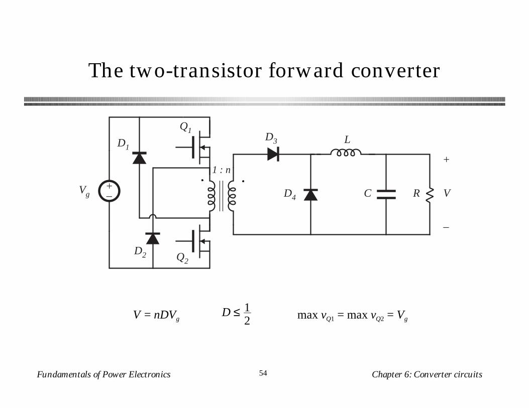
The two-transistor forward converter
+–
D1
Q1
1 : n
C R
+
V
–
L
D2
D3
Vg
Q2
D4
max vQ1 = max vQ2 = VgD ≤ 1
2V = nDVg

Fundamentals of Power Electronics Chapter 6: Converter circuits55
6.3.3. Push-pull isolated buck converter
C R
+
V
–
LD1
D2
1 : n
+–
Vg
Q1
Q2
+
vs(t)
–
–vT(t)
+
–vT(t)
+
iD1(t)
i(t)
V = nDVg 0 ≤ D ≤ 1

Fundamentals of Power Electronics Chapter 6: Converter circuits56
Waveforms: push-pull
iM(t)
vT(t)
vs(t)
iD1(t)
i(t)
Vg
0 0
–Vg
nVg
0
nVg
0
i0.5 i 0.5 i
0
∆iI
Vg
LM
– Vg
LM
t0 DTs Ts 2TsTs+DTs
Q1
D1 D2
D1Q2
D2 D2
D1conducting
devices:
• Used with low-voltage inputs
• Secondary-side circuit identical to full bridge
• As in full bridge, transformer volt-second balance is obtained over two switching periods
• Effect of nonidealities on transformer volt-second balance?
• Current programmed control can be used to mitigate transformer saturation problems. Duty cycle control not recommended.

Fundamentals of Power Electronics Chapter 6: Converter circuits57
6.3.4. Flyback converter
+– L
–
V
+
Vg
Q1 D1buck-boost converter:
construct inductor winding using two parallel wires:
+– L
–
V
+
Vg
Q1 D1
1:1

Fundamentals of Power Electronics Chapter 6: Converter circuits58
Derivation of flyback converter, cont.
+– LM
–
V
+
Vg
Q1 D1
1:1
Isolate inductor windings: the flyback converter
Flyback converter having a 1:n turns ratio and positive output:
+–
LM
+
V
–
Vg
Q1
D11:n
C

Fundamentals of Power Electronics Chapter 6: Converter circuits59
The “flyback transformer”
● A two-winding inductor● Symbol is same as
transformer, but function differs significantly from ideal transformer
● Energy is stored in magnetizing inductance
● Magnetizing inductance is relatively small
+–
LM
+
v
–Vg
Q1
D11:n
C
transformer model
iig
R
iC+
vL
–
● Current does not simultaneously flow in primary and secondary windings● Instantaneous winding voltages follow turns ratio
● Instantaneous (and rms) winding currents do not follow turns ratio● Model as (small) magnetizing inductance in parallel with ideal transformer

Fundamentals of Power Electronics Chapter 6: Converter circuits60
Subinterval 1
vL = Vg
iC = – vR
ig = i
CCM: small ripple approximation leads to
vL = Vg
iC = – VR
ig = I
+–
LM
+
v
–
Vg
1:n
C
transformer model
iig
R
iC+
vL
–

Fundamentals of Power Electronics Chapter 6: Converter circuits61
Subinterval 2
CCM: small ripple approximation leads to
vL = – vn
iC = in – v
Rig = 0
vL = – Vn
iC = In – V
Rig = 0
+–
+
v
–
Vg
1:n
C
transformer model
i
R
iC
i/n
–v/n
+
+
vL
–
ig=0

Fundamentals of Power Electronics Chapter 6: Converter circuits62
CCM Flyback waveforms and solution
vL
iC
ig
t
Vg
0
DTs D'TsTs
Q1 D1
conductingdevices:
–V/n
–V/R
I/n – V/R
I
Volt-second balance:
vL = D (Vg) + D' (– Vn ) = 0
Conversion ratio is
M(D) = VVg
= n DD'
Charge balance:
iC = D (– VR ) + D' ( I
n – VR ) = 0
Dc component of magnetizing current is
I = nVD'R
Dc component of source current is
Ig = ig = D (I) + D' (0)

Fundamentals of Power Electronics Chapter 6: Converter circuits63
Equivalent circuit model: CCM Flyback
vL = D (Vg) + D' (– Vn ) = 0
iC = D (– VR ) + D' ( I
n – VR ) = 0
Ig = ig = D (I) + D' (0)
+–
+– R
+
V
–
VgD'In
D'Vn
+–
DVgDI
IIg
+– R
+
V
–
Vg
IIg
1 : D D' : n

Fundamentals of Power Electronics Chapter 6: Converter circuits64
Discussion: Flyback converter
● Widely used in low power and/or high voltage applications● Low parts count● Multiple outputs are easily obtained, with minimum additional parts
● Cross regulation is inferior to buck-derived isolated converters● Often operated in discontinuous conduction mode● DCM analysis: DCM buck-boost with turns ratio

Fundamentals of Power Electronics Chapter 6: Converter circuits65
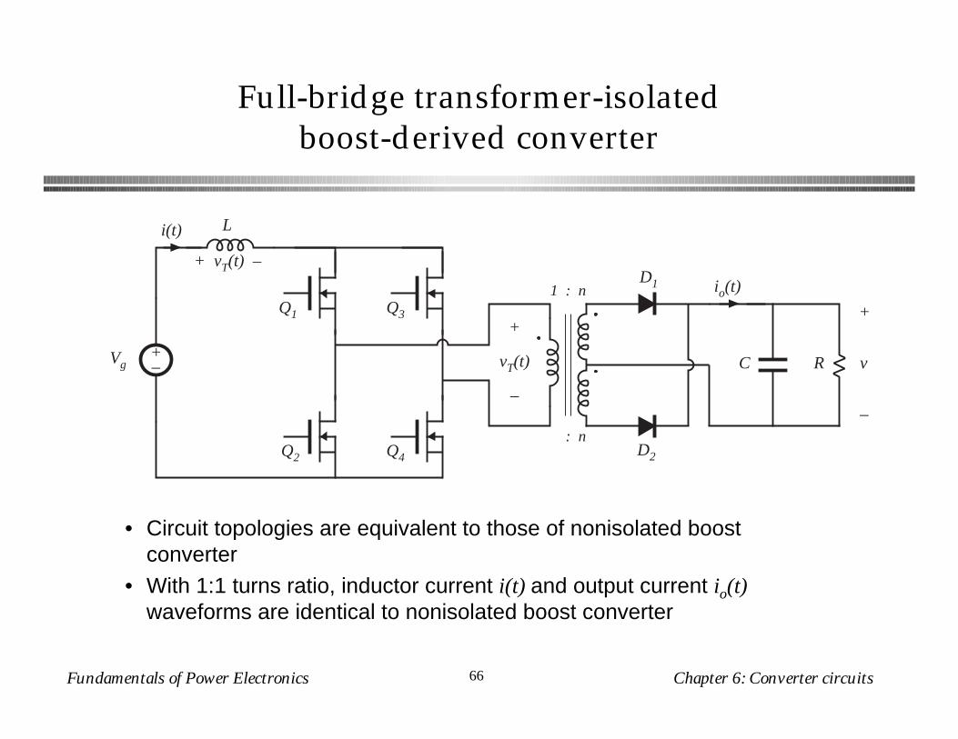
6.3.5. Boost-derived isolated converters
• A wide variety of boost-derived isolated dc-dc converters can be derived, by inversion of source and load of buck-derived isolated converters:
• full-bridge and half-bridge isolated boost converters
• inverse of forward converter: the “reverse” converter
• push-pull boost-derived converter
Of these, the full-bridge and push-pull boost-derived isolated converters are the most popular, and are briefly discussed here.
Fundamentals of Power Electronics Chapter 6: Converter circuits66
Full-bridge transformer-isolatedboost-derived converter
C R
+
v
–
L
D1
D2
1 : n
: n
i(t)
+
vT(t)
–
+–Vg
Q1
Q2
Q3
Q4
+ vT(t) –
io(t)
• Circuit topologies are equivalent to those of nonisolated boost converter
• With 1:1 turns ratio, inductor current i(t) and output current io(t) waveforms are identical to nonisolated boost converter

Fundamentals of Power Electronics Chapter 6: Converter circuits67
Transformer reset mechanism
• As in full-bridge buck topology, transformer volt-second balance is obtained over two switching periods.
• During first switching period: transistors Q1 and Q4 conduct for time DTs , applying volt-seconds VDTs to secondary winding.
• During next switching period: transistors Q2 and Q3 conduct for time DTs , applying volt-seconds–VDTs to secondary winding.
io(t)
t
0
Q1
D1
conductingdevices:
I/n
vT(t)
0 0
V/n
– V/n
I/n
0
DTs D'TsTs
DTs D'TsTs
Q2Q3Q4
Q1Q2Q3Q4
Q1Q4
Q2Q3D2
Fundamentals of Power Electronics Chapter 6: Converter circuits68
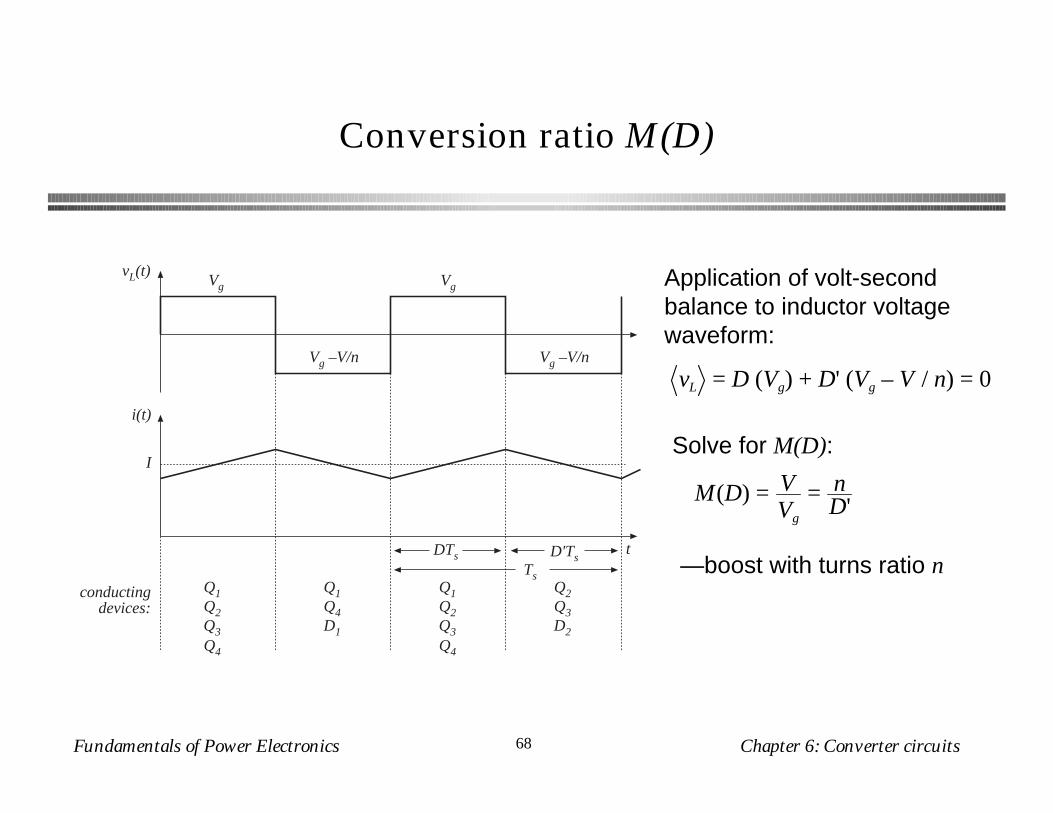
Conversion ratio M(D)
vL(t)
i(t)
t
Vg
Q1
D1
conductingdevices:
Vg –V/n
Vg
Vg –V/n
DTs D'TsTs
Q2Q3Q4
Q1Q2Q3Q4
Q1Q4
Q2Q3D2
I
Application of volt-second balance to inductor voltage waveform:
vL = D (Vg) + D' (Vg – V / n) = 0
Solve for M(D):
M(D) = VVg
= nD'
—boost with turns ratio n

Fundamentals of Power Electronics Chapter 6: Converter circuits69
Push-pull boost-derived converter
+–
Vg
C R
+
V
–
L
D1
D2
1 : n
Q1
Q2
+ vL(t) –
–vT(t)
+
–vT(t)
+
io(t)
i(t)
M(D) = VVg
= nD'

Fundamentals of Power Electronics Chapter 6: Converter circuits70
Push-pull converter based on Watkins-Johnson converter
+–
Vg
C R
+
V
–
D1
D2
1 : n
Q1
Q2

Fundamentals of Power Electronics Chapter 6: Converter circuits71
6.3.6. Isolated versions of the SEPIC and Cuk converter
+–
D1L1
C2
+
v
–
Q1
C1
L2RVg
+–
D1L1
C2
+
v
–
Q1
C1
RVg
1 : n
ip isi1
Basic nonisolated SEPIC
Isolated SEPIC

Fundamentals of Power Electronics Chapter 6: Converter circuits72
Isolated SEPIC
is(t)
i1(t)
i2(t)
t
Q1 D1
conductingdevices:
ip(t)
DTs D'TsTs
– i2
i1
0
(i1 + i2) / n
I1
I2
+–
D1L1
C2
+
v
–
Q1
C1
RVg
1 : nip
isi1 i2
ideal
transformermodel
LM
= L2
M(D) = VVg
= n DD'

Fundamentals of Power Electronics Chapter 6: Converter circuits73
Inverse SEPIC
+–
D1
L2
C2
+
v
–Q1
C1
RVg
1 : n
Isolated inverse SEPIC
Nonisolated inverse SEPIC
+– D1
L1 C2
+
v
–
Q1C1 L2
RVg

Fundamentals of Power Electronics Chapter 6: Converter circuits74
Obtaining isolation in the Cuk converter
+– D1
L1
C2 R
+
v
–
Q1
C1
L2
Vg
Nonisolated Cuk converter
+– D1
L1
C2 R
+
v
–
Q1
C1a L2
Vg
C1b
Split capacitor C1 into series capacitors C1a and C1b

Fundamentals of Power Electronics Chapter 6: Converter circuits75
Isolated Cuk converter
+– D1
L1
C2 R
+
v
–
Q1
C1a L2
Vg
C1b
1 : n
Insert transformer between capacitors C1a and C1b
Discussion
• Capacitors C1a and C1b ensure that no dc voltage is applied to transformer primary or secondary windings
• Transformer functions in conventional manner, with small magnetizing current and negligible energy storage within the magnetizing inductance
M(D) = VVg
= n DD'
Fundamentals of Power Electronics Chapter 6: Converter circuits76
6.4. Converter evaluation and design
For a given application, which converter topology is best?
There is no ultimate converter, perfectly suited for all possible applications
Trade studies
• Rough designs of several converter topologies to meet the given specifications
• An unbiased quantitative comparison of worst-case transistor currents and voltages, transformer size, etc.
Comparison via switch stress, switch utilization, and semiconductor cost
Spreadsheet design

Fundamentals of Power Electronics Chapter 6: Converter circuits77
6.4.1. Switch stress and switch utilization
• Largest single cost in a converter is usually the cost of the active semiconductor devices
• Conduction and switching losses associated with the active semiconductor devices often dominate the other sources of loss
This suggests evaluating candidate converter approaches by comparing the voltage and current stresses imposed on the active semiconductor devices.
Minimization of total switch stresses leads to reduced loss, and to minimization of the total silicon area required to realize the power devices of the converter.

Fundamentals of Power Electronics Chapter 6: Converter circuits78
Total active switch stress S
In a converter having k active semiconductor devices, the total active switch stress S is defined as
S = Vj I jΣj = 1
k
where
Vj is the peak voltage applied to switch j,
Ij is the rms current applied to switch j (peak current is also sometimes used).
In a good design, the total active switch stress is minimized.

Fundamentals of Power Electronics Chapter 6: Converter circuits79
Active switch utilization U
It is desired to minimize the total active switch stress, while maximizing the output power Pload.
The active switch utilization U is defined as
U =Pload
S
The active switch utilization is the converter output power obtained per unit of active switch stress. It is a converter figure-of-merit, which measures how well a converter utilizes its semiconductor devices.
Active switch utilization is less than 1 in transformer-isolated converters, and is a quantity to be maximized.
Converters having low switch utilizations require extra active silicon area, and operate with relatively low efficiency.
Active switch utilization is a function of converter operating point.

Fundamentals of Power Electronics Chapter 6: Converter circuits80
CCM flyback example: Determination of S
+–
LM
+
V
–
Vg
Q1
D11:n
C
During subinterval 2, the transistor blocks voltage VQ1,pk equal to Vg plus the reflected load voltage:
VQ1,pk = Vg + V / n =Vg
D'
ig
t
0
DTs D'TsTs
Q1 D1
conductingdevices:
I
Transistor current coincides with ig(t). RMS value is
IQ1,rms = I D =Pload
Vg D
Switch stress S is
S = VQ1,pk IQ1,rms = (Vg + V / n) (I D)

Fundamentals of Power Electronics Chapter 6: Converter circuits81
CCM flyback example: Determination of U
+– R
+
V
–
Vg
IIg
1 : D D' : n
CCM flyback model
Express load power Pload in terms of V and I:
Pload = D' V In
Previously-derived expression for S:
S = VQ1,pk IQ1,rms = (Vg + V / n) (I D)
U =Pload
S= D' D
Hence switch utilization U is

Fundamentals of Power Electronics Chapter 6: Converter circuits82
Flyback example: switch utilization U(D)
0
0.1
0.2
0.3
0.4
U
0 0.2 0.4 0.6 0.8 1
D
max U = 0.385 at D = 1/3For given V, Vg, Pload, the designer can arbitrarily choose D. The turns ratio n must then be chosen according to
n = VVg
D'D
Single operating point design: choose D = 1/3.
small D leads to large transistor current
large D leads to large transistor voltage

Fundamentals of Power Electronics Chapter 6: Converter circuits83
Comparison of switch utilizationsof some common converters
Table 6.1. Active switch utilizations of some common dc-dc converters, single operating point.
Converter U(D) max U(D) max U(D)occurs at D =
Buck D 1 1
Boost D'D
∞ 0
Buck-boost, flyback, nonisolated SEPIC, isolatedSEPIC, nonisolated Cuk, isolated Cuk
D' D 23 3
= 0.385 13
Forward, n1 = n2 12 D 1
2 2= 0.353 1
2Other isolated buck-derived converters (full-
bridge, half-bridge, push-pull) D
2 2 1
2 2= 0.353 1
Isolated boost-derived converters (full bridge,push-pull)
D'2 1 + D
12
0

Fundamentals of Power Electronics Chapter 6: Converter circuits84
Switch utilization : Discussion
● Increasing the range of operating points leads to reduced switch utilization● Buck converter
can operate with high switch utilization (U approaching 1) when D is close to 1
● Boost convertercan operate with high switch utilization (U approaching ∞) when D is
close to 1
● Transformer isolation leads to reduced switch utilization● Buck-derived transformer-isolated converters
U ≤ 0.353
should be designed to operate with D as large as other considerations allow
transformer turns ratio can be chosen to optimize design

Fundamentals of Power Electronics Chapter 6: Converter circuits85
Switch utilization: Discussion
● Nonisolated and isolated versions of buck-boost, SEPIC, and Cuk converters
U ≤ 0.385
Single-operating-point optimum occurs at D = 1/3
Nonisolated converters have lower switch utilizations than buck or boost
Isolation can be obtained without penalizing switch utilization
Fundamentals of Power Electronics Chapter 6: Converter circuits86
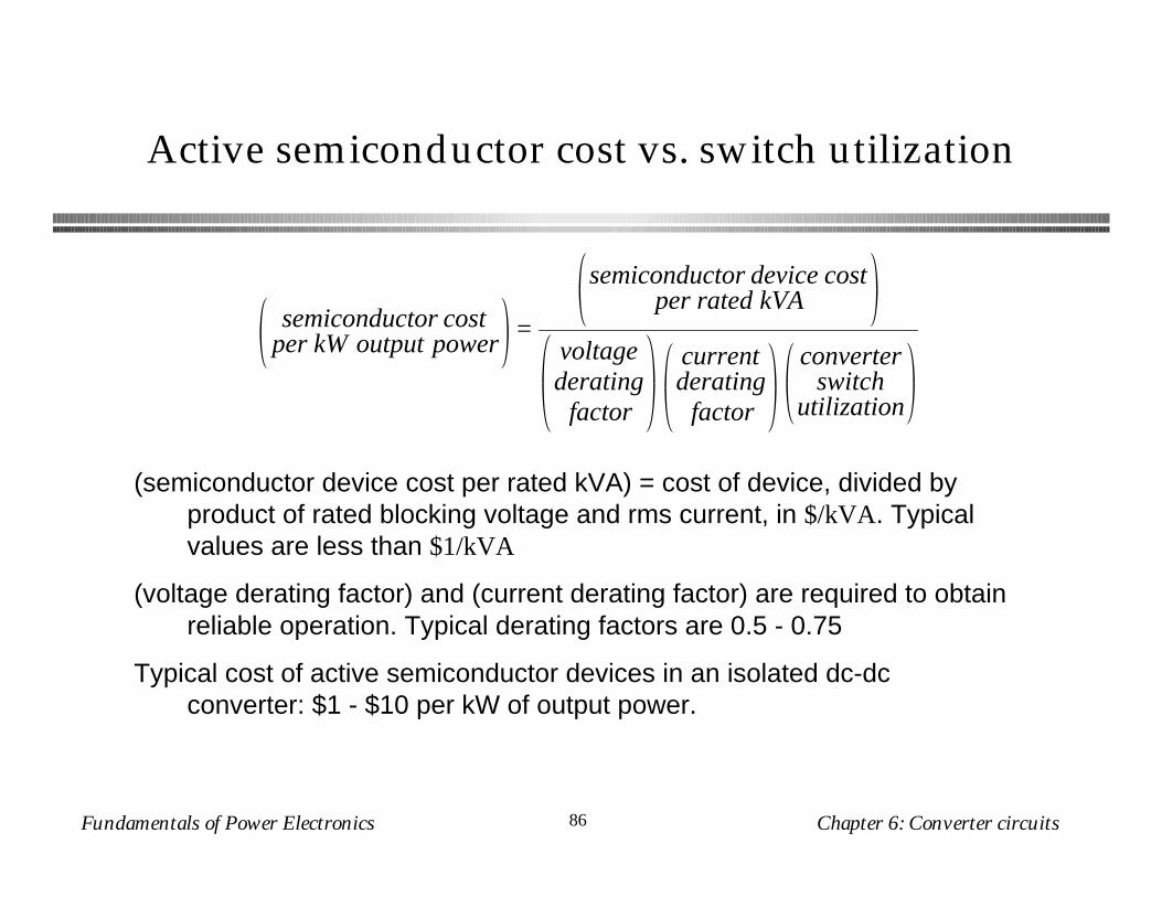
Active semiconductor cost vs. switch utilization
semiconductor costper kW output power
=
semiconductor device costper rated kVA
voltagederating
factor
currentderating
factor
converterswitch
utilization
(semiconductor device cost per rated kVA) = cost of device, divided by product of rated blocking voltage and rms current, in $/kVA. Typical values are less than $1/kVA
(voltage derating factor) and (current derating factor) are required to obtain reliable operation. Typical derating factors are 0.5 - 0.75
Typical cost of active semiconductor devices in an isolated dc-dc converter: $1 - $10 per kW of output power.

Fundamentals of Power Electronics Chapter 6: Converter circuits87
6.4.2. Converter design using computer spreadsheet
Given ranges of Vg and Pload , as well as desired value of V and other quantities such as switching frequency, ripple, etc., there are two basic engineering design tasks:
• Compare converter topologies and select the best for the given specifications
• Optimize the design of a given converter
A computer spreadsheet is a very useful tool for this job. The results of the steady-state converter analyses of chapters 1-6 can be entered, and detailed design investigations can be quickly performed:
• Evaluation of worst-case stresses over a range of operating points
• Evaluation of design tradeoffs

Fundamentals of Power Electronics Chapter 6: Converter circuits88
Spreadsheet design example
S peci fi cat ions
maximum input voltage Vg 390V
minimum input voltage Vg 260V
output voltage V 15V
maximum load power Pload 200W
minimum load power Pload 20W
switching frequency fs 100kHz
maximum output ripple ∆v 0.1V
• Input voltage: rectified 230Vrms ±20%
• Regulated output of 15V
• Rated load power 200W
• Must operate at 10% load
• Select switching frequency of 100kHz
• Output voltage ripple ≤ 0.1V
Compare single-transistor forward and flyback converters in this application
Specifications are entered at top of spreadsheet

Fundamentals of Power Electronics Chapter 6: Converter circuits89
Forward converter design, CCM
+–
D1
Q1
n1 : n2 : n3
C R
+
V
–
LD2
D3
Vg
Design variables
reset winding turns ratio n2 / n1 1
turns ratio n3 / n1 0.125
inductor current ripple ∆i 2A ref to sec
• Design for CCM at full load; may operate in DCM at light load

Fundamentals of Power Electronics Chapter 6: Converter circuits90
Flyback converter design, CCM
+–
LM
+
V
–
Vg
Q1
D11:n
C
Design variables
turns ratio n2 / n1 0.125
inductor current ripple ∆i 3A ref to sec
• Design for CCM at full load; may operate in DCM at light load

Fundamentals of Power Electronics Chapter 6: Converter circuits91
Enter results of converter analysis into spreadsheet(Forward converter example)
Maximum duty cycle occurs at minimum Vg and maximum Pload. Converter then operates in CCM, with
D =n1
n3
VVg
Inductor current ripple is
∆i =D' V Ts
2 L
Solve for L:
L =D' V Ts
2 ∆i
∆i is a design variable. For a given ∆i, the equation above can be used to determine L. To ensure CCM operation at full load, ∆i should be less than the full-load output current. C can be found in a similar manner.

Fundamentals of Power Electronics Chapter 6: Converter circuits92
Forward converter example, continued
Check for DCM at light load. The solution of the buck converter operating in DCM is
V =n3
n1
Vg2
1 + 4K / D2
with K = 2 L / R Ts, and R = V 2 / Pload
These equations apply equally well to the forward converter, provided that all quantities are referred to the transformer secondary side.
Solve for D:
D = 2 K2n3Vg
n1V– 1
2
– 1
D =n1
n3
VVg
in DCM in CCM
at a given operating point, the actual duty cycle is the small of the values calculated by the CCM and DCM equations above. Minimum D occurs at minimum Pload and maximum Vg.

Fundamentals of Power Electronics Chapter 6: Converter circuits93
More regarding forward converter example
Worst-case component stresses can now be evaluated.
Peak transistor voltage is
max vQ1 = Vg 1 +n1n2
Rms transistor current is
IQ1, rms =n3
n1
D I 2 + (∆i)2 / 3 ≈ n3
n1
D I
(this neglects transformer magnetizing current)
Other component stresses can be found in a similar manner. Magnetics design is left for a later chapter.

Fundamentals of Power Electronics Chapter 6: Converter circuits94
Results: forward and flyback converter spreadsheets
Forward conv ert er des ign, C CM Fl y back conv ert er desi gn, CC M
Design variables Design variables
reset winding turns ratio n2 / n1 1 turns ratio n2 / n1 0.125
turns ratio n3 / n1 0.125 inductor current ripple ∆i 3A ref to sec
inductor current ripple ∆i 2A ref to sec
Results Results
maximum duty cycle D 0.462 maximum duty cycle D 0.316
minimum D, at full load 0.308 minimum D, at full load 0.235
minimum D, at minimum load 0.251 minimum D, at minimum load 0.179
Worst-case stresses Worst-case stresses
peak transistor voltage vQ1 780V peak transistor voltage vQ1 510V
rms transistor current iQ1 1.13A rms transistor current iQ1 1.38A
transistor utilization U 0.226 transistor utilization U 0.284
peak diode voltage vD1 49V peak diode voltage vD1 64V
rms diode current iD1 9.1A rms diode current iD1 16.3A
peak diode voltage vD2 49V peak diode current iD1 22.2A
rms diode current iD2 11.1A
rms output capacitor current iC 1.15A rms output capacitor current iC 9.1A

Fundamentals of Power Electronics Chapter 6: Converter circuits95
Discussion: transistor voltage
Flyback converter
Ideal peak transistor voltage: 510V
Actual peak voltage will be higher, due to ringing causes by transformer leakage inductance
An 800V or 1000V MOSFET would have an adequate design margin
Forward converter
Ideal peak transistor voltage: 780V, 53% greater than flyback
MOSFETs having voltage rating greater than 1000V are not available (in 1995) —when ringing due to transformer leakage inductance is accounted for, this design will have an inadequate design margin
Fix: use two-transistor forward converter, or change reset winding turns ratio
A conclusion: reset mechanism of flyback is superior to forward

Fundamentals of Power Electronics Chapter 6: Converter circuits96
Discussion: rms transistor current
Forward
1.13A worst-case
transistor utilization 0.226
Flyback
1.38A worst case, 22% higher than forward
transistor utilization 0.284
CCM flyback exhibits higher peak and rms currents. Currents in DCM flyback are even higher

Fundamentals of Power Electronics Chapter 6: Converter circuits97
Discussion: secondary-side diode and capacitor stresses
Forward
peak diode voltage 49V
rms diode current 9.1A / 11.1A
rms capacitor current 1.15A
Flyback
peak diode voltage 64V
rms diode current 16.3A
peak diode current 22.2A
rms capacitor current 9.1A
Secondary-side currents, especially capacitor currents, limit the practical application of the flyback converter to situations where the load current is not too great.

Fundamentals of Power Electronics Chapter 6: Converter circuits98
Summary of key points
1. The boost converter can be viewed as an inverse buck converter, while the buck-boost and Cuk converters arise from cascade connections of buck and boost converters. The properties of these converters are consistent with their origins. Ac outputs can be obtained by differential connection of the load. An infinite number of converters are possible, and several are listed in this chapter.
2. For understanding the operation of most converters containing transformers, the transformer can be modeled as a magnetizing inductance in parallel with an ideal transformer. The magnetizing inductance must obey all of the usual rules for inductors, including the principle of volt-second balance.

Fundamentals of Power Electronics Chapter 6: Converter circuits99
Summary of key points
3. The steady-state behavior of transformer-isolated converters may be understood by first replacing the transformer with the magnetizing-inductance-plus-ideal-transformer equivalent circuit. The techniques developed in the previous chapters can then be applied, including use of inductor volt-second balance and capacitor charge balance to find dc currents and voltages, use of equivalent circuits to model losses and efficiency, and analysis of the discontinuous conduction mode.
4. In the full-bridge, half-bridge, and push-pull isolated versions of the buck and/or boost converters, the transformer frequency is twice the output ripple frequency. The transformer is reset while it transfers energy: the applied voltage polarity alternates on successive switching periods.

Fundamentals of Power Electronics Chapter 6: Converter circuits100
Summary of key points
5. In the conventional forward converter, the transformer is reset while the transistor is off. The transformer magnetizing inductance operates in the discontinuous conduction mode, and the maximum duty cycle is limited.
6. The flyback converter is based on the buck-boost converter. The flyback transformer is actually a two-winding inductor, which stores and transfers energy.
7. The transformer turns ratio is an extra degree-of-freedom which the designer can choose to optimize the converter design. Use of a computer spreadsheet is an effective way to determine how the choice of turns ratio affects the component voltage and current stresses.
8. Total active switch stress, and active switch utilization, are two simplified figures-of-merit which can be used to compare the various converter circuits.