chapter 2 experimental techniques for the synthesis...
TRANSCRIPT

38
CHAPTER 2
EXPERIMENTAL TECHNIQUES FOR THE SYNTHESIS
AND CHARACTERIZATION OF NANOMATERIALS
2.1. Introduction:
In order to explore novel physical properties and phenomena
and realize potential applications of nanostructures and
nanomaterials, the ability to fabricate and process nanomaterials
and nanostructures is the first corner stone in nanotechnology.
There exist a number of methods to synthesize the nanomaterials
which are categorized in two techniques “top down and bottom up”.
Solid state route, ball milling comes in the category of top down
approach, while wet chemical routes like sol-gel, co-precipitation,
etc. come in the category of bottom up approach. Secondly,
characterization of nanomaterials is necessary to analyze their
various properties. Therefore, this chapter describes the various
methods of synthesis and characterization of nanomaterials.
Characterization techniques include XRD, SEM, TEM, EDAX, UV-
Visible spectroscopy, FTIR spectroscopy, etc.
2.2. Synthesis of Nanomaterials:
Fabrication of nanomaterials with strict control over size,
shape, and crystalline structure has become very important for the
applications of nanotechnology in numerous fields including
catalysis, medicine, and electronics. Synthesis methods for
nanoparticles are typically grouped into two categories: “top-down”

39
and “bottom-up” approach. The first involves the division of a
massive solid into smaller and smaller portions, successively
reaching to nanometer size. This approach may involve milling or
attrition. The second, “bottom-up”, method of nanoparticle
fabrication involves the condensation of atoms or molecular entities
in a gas phase or in solution to form the material in the nanometer
range. The latter approach is far more popular in the synthesis of
nanoparticles owing to several advantages associated with it. Fig. 2.1
shows the general overview of the two approaches. There are many
bottom up methods of synthesizing metal oxide nanomaterials, such
as hydrothermal, [1, 2] combustion synthesis [3], gas-phase methods
[4, 5], microwave synthesis and sol-gel processing [6]. Sol-gel
processing techniques will be discussed in detail in this chapter
because the materials reported in subsequent chapters were
fabricated using this method. However, an overview of other
techniques usually employed for the synthesis of nanomaterials is
also discussed hereunder.

40
Fig.2.1. Schematic of Bottom-up and Top-down approaches
2.2.1. Combustion route:
Combustion synthesis leads to highly crystalline particles with
large surface areas [7, 8]. The process involves a rapid heating of a
solution containing redox groups [9]. During combustion, the
temperature reaches approximately 650 °C for one or two minutes
making the material crystalline.
2.2.2. Hydrothermal method:
Hydrothermal synthesis is typically carried out in a
pressurized vessel called an autoclave with the reaction in aqueous
solution [10]. The temperature in the autoclave can be raised above
the boiling point of water, reaching the pressure of vapour
saturation. Hydrothermal synthesis is widely used for the

41
preparation of metal oxide nanoparticles which can easily be
obtained through hydrothermal treatment of peptized precipitates of
a metal precursor with water [10, 11]. The hydrothermal method can
be useful to control grain size, particle morphology, crystalline phase
and surface chemistry through regulation of the solution
composition, reaction temperature, pressure, solvent properties,
additives and aging time [9].
2.2.3. Gas phase methods:
Gas phase methods are ideal for the production of thin films.
Gas phase synthesis can be carried out chemically or physically.
Chemical vapour deposition (CVD) is a widely used industrial
technique that can coat large areas in a short space of time [9].
During the procedure, metal oxide is formed from a chemical
reaction or decomposition of a precursor in the gas phase [12, 13].
Physical vapour deposition (PVD) is another thin film
deposition technique. The process is similar to chemical vapour
deposition (CVD) except that the raw materials/precursors, i.e. the
material that is going to be deposited starts out in solid form,
whereas in CVD, the precursors are introduced to the reaction
chamber in the gaseous state. The process proceeds atomistically
and mostly involves no chemical reactions. Various methods have
been developed for the removal of growth species from the source or
target. The thickness of the deposits can vary from angstroms to
millimeters. In general, these methods can be divided into two

42
groups: evaporation and sputtering. In evaporation, the growth
species are removed from the source by thermal means. In
sputtering, atoms or molecules are dislodged from solid target
through impact of gaseous ions (plasma) [14].
2.2.4. Microwave synthesis:
Microwave synthesis is relatively new and an interesting
technique for the synthesis of oxide materials [15]. Various
nanomaterials have been synthesized in remarkably short time
under microwave irradiation [16, 17]. Microwave techniques
eliminate the use of high temperature calcination for extended
periods of time and allow for fast, reproducible synthesis of
crystalline metal oxide nanomaterials. Utilizing microwave energy for
the thermal treatment generally leads to a very fine particle in the
nanocrystalline regime because of the shorter synthesis time and a
highly focused local heating.
2.2.5. Sol-gel method:
The sol-gel process is a capable wet chemical process to make
ceramic and glass materials. This synthesis technique involves the
conversion of a system from a colloidal liquid, named sol, into a
semi-solid gel phase [18, 19, 20]. The sol-gel technology can be used
to prepare ceramic or glass materials in a wide variety of forms:
ultra-fine or spherical shaped powders, thin film coatings, ceramic
fibres, microporous inorganic membranes, monolithics, or extremely

43
porous aerogels. An overview of the sol-gel process is illustrated in
Fig. 2.2.
This technique offers many advantages including the low
processing temperature, the ability to control the composition on
molecular scale and the porosity to obtain high surface area
materials, the homogeneity of the final product up to atomic scale.
Moreover, it is possible to synthesize complex composition materials,
to form higher purity products through the use of high purity
reagents. The sol-gel process allows obtaining high quality films up
to micron thickness, difficult to obtain using the physical deposition
techniques. Moreover, it is possible to synthesize complex
composition materials and to provide coatings over complex
geometries [18, 19, 20].
Fig.2.2. Mechanism of Sol-gel process

44
The starting materials used in the preparation of the sol are
usually inorganic metal salts or metal organic compounds, which by
hydrolysis and polycondensation reactions form the sol [18, 19, 20].
Further processing of the sol enables one to make ceramic materials
in different forms. Thin films can be produced by spin-coating or dip-
coating. When the sol is cast into a mould, a wet gel will form. By
drying and heat-treatment, the gel is converted into dense ceramic or
glass materials. If the liquid in a wet gel is removed under a
supercritical condition, a highly porous and extremely low density
aerogel material is obtained. As the viscosity of a sol is adjusted into
a suitable viscosity range, ceramic fibres can be drawn from the sol.
Ultra-fine and uniform ceramic powders are formed by precipitation,
spray pyrolysis, or emulsion techniques.
2.3. Characterization Techniques:
2.3.1. X-ray Diffraction:
The German Physicist, Von Laue in 1912 was the first who
took up the problem of X-ray diffraction (XRD) with the cause that,
“if crystals were composed of regularly spaced atoms which might act
as scattering centers for x-rays, and if X-rays were electromagnetic
waves of wavelength about equal to the inter atomic distances in
crystals, then it should be possible to diffract X-rays by means of
crystals” [21]. Now a days, X-ray diffraction is most extensively used
technique for the characterization of the materials. A lot of
information can be extracted from the XRD data. This is an

45
appropriate technique for all forms of samples, i.e. powder and bulk
as well as thin film. Using this technique, one can get the
information regarding the crystalline nature of a material, nature of
the phase present, lattice parameter and grain size [22]. From the
position and shape of the lines, one can obtain information regarding
the unit cell parameters and microstructural parameters (grain size,
microstrain, etc), respectively. In case of thin films, the change in
lattice parameter with respect to the bulk gives the idea about the
nature of strain present in the system.
The interaction of X-ray radiation with crystalline sample is
governed by Bragg’s law, which depicts a relationship between the
diffraction angles (Bragg angle), X-ray wavelength, and interplanar
spacing of the crystal planes. According to Bragg’s law, the X-ray
diffraction can be visualized as X-rays reflecting from a series of
crystallographic planes as shown in Fig. 2.3. The path differences
introduced between a pair of waves travelled through the neighboring
crystallographic planes are determined by the interplanar spacing. If
the total path difference is equal to nλ (n being an integer), the
constructive interference will occur and a group of diffraction peaks
can be observed, which give rise to X-ray patterns. The quantitative
account of Bragg’s law can be expressed as:
2dhkl
sin θ = nλ
where d is the interplanar spacing for a given set of hkl and θ the
Bragg angle.

46
Fig.2.3. Geometrical illustrations of crystal planes and Bragg’s law.
Fig.2.4. X-ray Diffractometer (XRD) machine.
The XRD measurements were carried out using Rigaku X-ray
diffractometer with CuKα (λ = 1.54187Å) radiation at room

47
temperature, shown in Fig. 2.4, and operated at a voltage of 30kV
and filament current of 40mA. The phase identification for all the
samples reported in this thesis was performed by matching the peak
positions and intensities in XRD patterns to those patterns in the
JCPDS (Joint Committee on Powder Diffraction Standards) database.
The diffraction method is based on the effect of broadening of
diffraction reflections associated with the size of the particles
(crystallites). All types of defects cause displacement of the atoms
from the lattice sites. M.A. Krivoglaz in 1969 [23] derived an equation
for the intensity of the Bragg reflections from a crystal defect, which
enabled all the defects to be derived conventionally into two groups.
The defects in the first group only lower the intensity of the
diffraction reflections but do not cause the reflection broadening. The
broadening of the reflections is caused by the defects of second
group. These defects are micro-deformations, inhomogeneity (non-
uniform composition of the substance over their volume) and the
small particle size. The size of nanomaterials can be derived from the
peak broadening and can be calculated by using the Scherrer
equation (2.2), provided that the nanocrystalline size is less than
100nm.
cos
kD
where D is the average crystallite dimension perpendicular to the
reflecting phases, λ the X-ray wavelength, k the Scherrer constant

48
which equals 0.9 for spherical particles, whose value depends on the
shape of the particle (crystallite, domain) and on diffraction reflection
indices (hkl), and β is the full width at half maximum of the peaks.
The Scherrer formula is quite satisfactory for small grains (large
broadening) in the absence of significant microstrain. A microstrain
describes the relative mean square deviation of the lattice spacing
from its mean value. Based on the grain size dependence of the
strain it is reasonable to assume that there is a radial strain
gradient, but from X-ray diffraction only a homogeneous, volume-
averaged value is obtained.
2.3.2. Scanning Electron Microscopy (SEM):
Electron microscopes are scientific instruments that use a
beam of energetic electrons to examine objects on a very fine scale.
Electron microscopes were developed due to the limitations of Light
Microscopes which are limited by the physics of light. In the early
1930's this theoretical limit had been reached and there was a
scientific desire to see the fine details of the interior structures of
organic cells (nucleus, mitochondria...etc.). This required 10,000X
plus magnification which was not possible using existing optical
microscopes.
The first Scanning electron microscope (SEM) debuted in 1938
(Von Ardenne) with the first commercial instruments around 1965.
Its late development was due to the electronics involved in "scanning"
the beam of electrons across the sample. Scanning electron

49
microscopy (SEM) can provide a highly magnified image of the
surface and the composition information of near surface regions of a
material [24]. The resolution of SEM can approach a few nanometers
and the magnifications of SEM can be easily adjusted from about 10
times to 300,000 times. In SEM, electron beam, accelerated by a
relatively low voltage of 1-20 kV, is scanned on the specimen surface.
As the electron beam strikes the surface, a large number of signals
are generated from (or through) the surface in the form of electrons
or photons. These signals emitted from the specimen are collected by
detectors to form images and the images are displayed on a cathode
ray tube screen. There are three types of images produced in SEM:
secondary electron images, backscattered electron images, and
elemental X-ray maps. Secondary electrons (SE) are considered to be
the electrons resulted from inelastic scattering with atomic electrons
and with the energy less than 50 eV. The secondary emission of
electrons from the specimen surface is usually confined to an area
near the beam impact zone that permits images to be obtained at
high resolution. These images, as seen on a cathode ray tube,
provide a three dimensional appearance due to the large depth of
field of the SEM as well as the shadow relief of the secondary
electrons contrast. Backscattered electrons (BSE) are considered to
be the electrons resulted from elastic scattering with the atomic
nucleus and with the energy greater than 50 eV [24]. The
backscattering will likely occur in a material of higher atomic

50
number, so the contrast caused by elemental differences can be built
up. After the primary electron beam collides with an atom in the
specimen and ejects a core electron from the atom, the excited atom
then decays to its ground state and emit either a characteristic X-ray
photon or an Auger electron [25]. The energy dispersive X-ray
detector (EDX) can sort the X-ray signal by energy and produce
elemental images, so the spatial distribution of particular elements
can be detected by SEM. SEM usually has resolution of 1 nm for 1
KV, even resolution of 0.6 nm is possible for 5 KV.
Fig.2.5. Schematic details of SEM
2.3.3. Transmission Electron microscopy (TEM):
Transmission electron microscopy (TEM) is a microscopy
technique where a beam of electrons is transmitted through an ultra
thin specimen, interacting with the specimen as it passes through.

51
An image is formed from the interaction of the electrons transmitted
through the specimen; the image is magnified and focused onto an
imaging device, such as a fluorescent screen, on a layer of
photographic film, or to be detected by a sensor such as a CCD
camera.
TEMs are capable of imaging at a significantly
higher resolution than light microscopes, owing to the small de
Broglie wavelength of electrons. This enables the instrument's user
to examine fine detail- even as small as a single column of atoms,
which is tens of thousands times smaller than the smallest
resolvable object in a light microscope. TEM forms a major analysis
method in a range of scientific fields, in both physical and biological
sciences. TEMs find application in cancer research, virology,
materials science as well as pollution and semiconductor research.
At smaller magnifications TEM image contrast is due to
absorption of electrons in the material, due to the thickness and
composition of the material. At higher magnifications complex wave
interactions modulate the intensity of the image, requiring expert
analysis of observed images. Alternate modes of use allow for the
TEM to observe modulations in chemical identity, crystal orientation,
electronic structure and sample induced electron phase shift as well
as the regular absorption based imaging.
The first TEM was built by Max Knoll and Ernst Ruska in
1931, with this group developing the first TEM with resolving

52
power greater than that of light in 1933 and the first commercial
TEM in 1939.
Theoretically, the maximum resolution, d, that one can obtain
with a light microscope has been limited by the wavelength of
the photons that are being used to probe the sample, λ and
the numerical aperture of the system, NA [26].
Early twentieth century scientist’s theorized ways of getting
around the limitations of the relatively large wavelength of visible
light (wavelengths of 400–700 nanometers) by using electrons. Like
all matter, electrons have both wave and particle properties (as
theorized by Louis-Victor de Broglie), and their wave-like properties
mean that a beam of electrons can be made to behave like a beam of
electromagnetic radiation. The wavelength of electrons is found by
equating the de Broglie equation to the kinetic energy of an electron.
An additional correction must be made to account for relativistic
effects, as in TEM an electron’s velocity approaches the speed of
light, c [27].
where, h is Planck's constant, m0 is the rest mass of an electron
and E is the energy of the accelerated electron. Electrons are usually
generated in an electron microscope by a process known as
thermionic emission from a filament, usually tungsten, in the same

53
manner as a light bulb, or alternatively by field electron emission
[28]. The electrons are then accelerated by an electric potential
(measured in volts) and focused by electrostatic and electromagnetic
lenses onto the sample. The transmitted beam contains information
about electron density, phase and periodicity; this beam is used to
form an image.
Fig.2.6. Layout of optical components in a basic TEM
Components:
A TEM is composed of several components, which include a
vacuum system in which the electrons travel an electron emission
source for generation of the electron stream, a series of
electromagnetic lenses, as well as electrostatic plates. The latter two

54
allow the operator to guide and manipulate the beam as required.
Also required is a device to allow the insertion into, motion within,
and removal of specimens from the beam path. Imaging devices are
subsequently used to create an image from the electrons that exit the
system.
Fig.2.7. Transmission electron microscope (TEM)
Electron gun:
The electron gun is formed from several components: the
filament, a biasing circuit, a Wehnelt cap, and an extraction anode.
By connecting the filament to the negative component power supply,
electrons can be "pumped" from the electron gun to the anode plate,
and TEM column, thus completing the circuit. The gun is designed to
create a beam of electrons exiting from the assembly at some given

55
angle, known as the gun divergence semi angle, α. By constructing
the Wehnelt cylinder such that it has a higher negative charge than
the filament itself, electrons that exit the filament in a diverging
manner are, under proper operation, forced into a converging pattern
the minimum size of which is the gun crossover diameter.
Fig.2.8. Cross sectional diagram of an electron gun assembly,
illustrating electron extraction.
The thermionic emission current density, J, can be related to
the work function of the emitting material and is a Boltzmann
distribution given below, where A is a constant, Φ is the work
function and T is the temperature of the material [29].
This equation shows that in order to achieve sufficient current
density it is necessary to heat the emitter, taking care not to cause

56
damage by application of excessive heat, for this reason materials
with either a high melting point, such as tungsten, or those with a
low work function (LaB6) are required for the gun filament.
Furthermore both lanthanum hexaboride and tungsten
thermionic sources must be heated in order to achieve thermionic
emission, this can be achieved by the use of a small resistive strip.
To prevent thermal shock, there is often a delay enforced in the
application of current to the tip, to prevent thermal gradients from
damaging the filament, the delay is usually a few seconds for LaB6,
and significantly lower for tungsten.
2.3.4. Optical spectroscopy:
Optical spectroscopy has been widely used for the
characterization of nanomaterials and the techniques can be
generally categorized into two groups: absorption and emission
spectroscopy and vibrational spectroscopy. The former determines
the electronic structures of atoms, ions, molecules or crystals
through exciting electrons from the ground to excited states
(absorption) and relaxing from the excited to ground states
(emission). The vibrational techniques may be summarized as
involving the interactions of photons with species in a sample that
results in energy transfer to or from the sample via vibrational
excitation or de-excitation. The vibrational frequencies provide the
information of chemical bonds in the detecting samples. Infra red

57
and Raman spectroscopy are the examples of vibrational
spectroscopy.
2.3.4.1. UV-Visible Spectroscopy:
Ultraviolet-visible (UV-vis) spectroscopy is widely utilized to
quantitatively characterize organic and inorganic nanosized
molecules. A sample is irradiated with electromagnetic waves in the
ultraviolet and visible ranges and the absorbed light is analyzed
through the resulting sprectrum [30, 31]. It can be employed to
identify the constituents of a substance, determine their
concentrations, and to identify functional groups in molecules. The
samples can be either organic or inorganic, and may exist in
gaseous, liquid or solid form. Different sized materials can be
characterized, ranging from transition metal ions and small
molecular weight organic molecules, whose diameters can be several
Ångstroms, to polymers, supramolecular assemblies, nano-particles
and bulk materials. Size dependant properties can also be observed
in a UV-visible spectrum, particularly in the nano and atomic scales.
These include peak broadening and shifts in the absorption
wavelength. Many electronic properties, such as the band gap of a
material, can also be determined by this technique. The energies
associated with UV-visible ranges are sufficient to excite molecular
electrons to higher energy orbitals [32, 33]. Photons in the visible
range have wavelengths between 800-400 nm, which corresponds to
energies between 36 and 72 kcal/mol. The near UV range includes

58
wavelengths down to 200 nm, and has energies as high as 143
kcal/mol. UV radiations of lower wavelengths is difficult to handle for
safety reasons, and is rarely used in routine UV-vis spectroscopy.
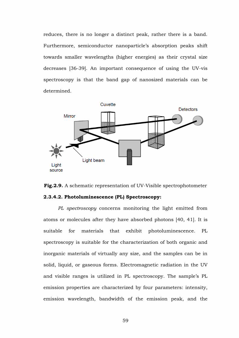
Fig. 2.9 shows a typical UV-vis absorption experiment for a liquid
sample. A beam of monochromatic light is split into two beams, one
of them is passed through the sample, and the other passes a
reference (in this figure, a solvent in which the sample is dissolved)
[34]. After transmission through the sample and reference, the two
beams are directed back to the detectors where they are compared.
The difference between the signals is the basis of the measurement.
Liquid samples are usually contained in a cell (called a cuvette) that
has flat, fused quartz faces. Quartz is commonly used as it is
transparent to both UV and visible lights.
UV-vis spectroscopy offers a relatively straight forward and
effective way for quantitatively characterizing both organic and
inorganic nanomaterials. Furthermore, as it operates on the principle
of absorption of photons that promotes the molecule to an excited
state; it is an ideal technique for determining the electronic
properties of nanomaterials. In the spectrum of nanoparticles, the
absorption peak’s width strongly depends on the chemical
composition and the particle size. As a result, their spectrum is
different from their bulk counterparts. For instance, for
semiconductor nanocrystals, the absorption spectrum is broadened
owing to quantum confinement effects, [35, 36] and as their size
59
reduces, there is no longer a distinct peak, rather there is a band.
Furthermore, semiconductor nanoparticle’s absorption peaks shift
towards smaller wavelengths (higher energies) as their crystal size
decreases [36-39]. An important consequence of using the UV-vis
spectroscopy is that the band gap of nanosized materials can be
determined.
Fig.2.9. A schematic representation of UV-Visible spectrophotometer
2.3.4.2. Photoluminescence (PL) Spectroscopy:
PL spectroscopy concerns monitoring the light emitted from
atoms or molecules after they have absorbed photons [40, 41]. It is
suitable for materials that exhibit photoluminescence. PL
spectroscopy is suitable for the characterization of both organic and
inorganic materials of virtually any size, and the samples can be in
solid, liquid, or gaseous forms. Electromagnetic radiation in the UV
and visible ranges is utilized in PL spectroscopy. The sample’s PL
emission properties are characterized by four parameters: intensity,
emission wavelength, bandwidth of the emission peak, and the

60
emission stability [42]. The PL properties of a material can change in
different ambient environments, or in the presence of other
molecules. Furthermore, as dimensions are reduced to the
nanoscale, PL emission properties can change, in particular a size
dependent shift in the emission wavelength can be observed.
Additionally, because the released photon corresponds to the energy
difference between the states, PL spectroscopy can be utilized to
study material properties such as band gap, recombination
mechanisms, and impurity levels. In a typical PL spectroscopy setup
for liquid samples (Fig. 2.10), a solution containing the sample is
placed in a quartz cuvette with a known path length. Double beam
optics is generally employed. The first beam passes through an
excitation filter or monochromator, then through the sample and
onto a detector. This impinging light causes photoluminescence,
which is emitted in all directions. A small portion of the emitted light
arrives at the detector after passing through an optional emission
filter or monochromator [43]. A second reference beam is attenuated
and compared with the beam from the sample. Solid samples can
also be analyzed, with the incident beam impinging on the material
(thin film, powder etc.). Generally an emission spectrum is recorded,
where the sample is irradiated with a single wavelength and the
intensity of the luminescence emission is recorded as a function of
wavelength. The fluorescence of a sample can also be monitored as a

61
function of time, after excitation by a flash of light. This technique is
called time resolved fluorescence spectroscopy.
Fig.2.10. PL spectrophotometer set up
2.3.4.3. Infrared Spectroscopy:
Infrared (IR) spectroscopy is a popular characterization
technique in which a sample is placed in the path of an IR radiation
source and its absorption of different IR frequencies is measured [44,
45]. Solid, liquid, and gaseous samples can all be characterized by
this technique. IR photons energies, in a range between 1 to 15
kcal/mol, are insufficient to excite electrons to higher electronic
energy states, but transitions in vibrational energy states (see Fig.

62
2.11). These states are associated with a molecule’s bonds, and
consequently
Fig.2.11. Possible physical processes following absorption of a
photon
Each molecule has its own unique signatures. Therefore, IR
spectroscopy may be employed to identify the type of bond between
two or more atoms and consequently identify functional groups. IR
spectroscopy is also widely used to characterize the attachment of
organic ligands to organic/inorganic nanoparticles and surfaces.
Because IR spectroscopy is quantitative, the number of a type of
bond may be determined. Virtually all organic compounds absorb IR
radiation, but inorganic materials are less commonly characterized,
as heavy atoms show vibrational transitions in the far IR region, with

63
some having extremely broad peaks that hampers the identification
of the functional groups. Furthermore, the peak intensities of some
ionic inorganic compounds may be too weak to be measured [46, 47].
The covalent bonds that hold molecules together are neither stiff nor
rigid, but rather they vibrate at specific frequencies corresponding to
their vibrational energy levels. The vibration frequencies depend on
several factors including bond strength and the atomic mass. The
bonds can be modified in different ways, in a similar manner to a
spring. Chemical bonds may be contorted in six different ways:
stretching (both symmetrical and asymmetrical), scissoring, rocking,
wagging, and twisting. Absorption of IR radiation causes the bond to
move from the lowest vibrational state to the next highest, and the
energy associated with absorbed IR radiation is converted into these
types of motions [48, 49, 50] Other rotational motions usually
accompany these individual vibrational motions. These combinations
lead to absorption bands, not discrete lines, which are commonly
observed in the mid IR region [50]. Weaker bonds require less energy
to be absorbed and behave as though the bonds are springs that
have different strengths. More complex molecules contain dozens or
even hundreds of different possible bond stretches and bending
motions, which implies the spectrum may contain dozens or
hundreds of absorption lines. This means that the IR absorption
spectrum can be its unique fingerprint for identification of a molecule
[51]. The fingerprint region contains wavenumbers between 400 and

64
1500 cm–1. A diatomic molecule, that has only one bond, can only
vibrate in one direction. For a linear molecule (e.g. hydrocarbons)
with n atoms, there are 3n-5 vibrational modes. If the molecule is
non-linear (such as methane, aromatics etc.), then there will be 3n-6
modes. Samples can be prepared in several ways for an IR
measurement. For powders, a small amount of the sample is added
to potassium bromide (KBr), after which this mixture is ground into a
fine powder and subsequently compressed into a small, thin, quasi-
transparent disc (Fig. 2.11). For liquids, a drop of sample may be
sandwiched between two salt plates, such as NaCl, KBr and NaCl are
chosen as neither of these compound shows an IR active stretch in
the region typically observed for organic and some inorganic
molecules.
Fig.2.12. Various processes to take the IR spectra
2.3.5. Electron spectroscopy:
In this section we shall discuss Energy dispersive X-ray
spectroscopy (EDS) and X-ray photoelectron spectroscopy (XPS). The
electron spectroscopy relies on the unique energy levels of the
emission of photons (X-ray) or electrons ejected from the atoms in

65
question. When an incident electron or photon, such as X-ray or γ-
ray, strikes an unexcited atom, an electron from an inner shell is
ejected and leaves a hole or electron vacancy in the inner shell. An
electron from an outer shell fills the hole by lowering its energy, and
simultaneously the excess energy is released through either emission
of an X-ray, which is used in EDS, or ejection of a third electron that
is known as auger electron, from a further outer shell, which is used
in Auger Electron spectroscopy (AES). If incident photons are used
for excitation, the resulting characteristic X-rays are known as
fluorescent X-rays. Since each atom in the Periodic Table has a
unique electronic structure with unique set of energy levels, both X-
ray and Auger spectral lines are characteristic of the element under
investigation. By measuring the energies of the X-rays and Auger
electrons emitted by a material, its chemical composition can be
determined.

66
Fig. 2.13. Schematic of electron energy transitions: (a) initial state, (b) incident photon or electron ejects K shell electron, (c) X-ray emission when 2s electron fills electron hole, and (d)
Auger electron emission with a KLL transition. [M. Orhring, The Materials Science of Thin Films, Academic
Press, San Diego, CA, 1992.1]
A similar principle is applicable to XPS. In XPS, relatively low
energy X-rays are used to eject the electrons from an atom via the
photoelectric effect. In XPS the sample is irradiated with a beam of
usually monochromatic, low-energy X-rays. Photoelectron emission
results from the atoms in the specimen surface, and the kinetic
energy distribution of the ejected photoelectrons is measured directly
using an electron spectrometer. Each surface atom possesses core-
level electrons that are not directly involved with chemical bonding
but are influenced slightly by the chemical environment of the atom.

67
The binding energy of each core-level electron (approximately its
ionization energy) is characteristic of the atom and specific orbital to
which it belongs. Since the energy of the incident X-rays is known,
the measured kinetic energy of a core-level photoelectron peak can
be related directly to its characteristic binding energy. The binding
energies of the various photoelectron peaks (1s, 2s, 2p, etc.) are well
tabulated and XPS therefore provides a means of elemental
identification which can also be quantified via measurement of
integrated photoelectron peak intensities and the use of a standard
set of sensitivity factors to give a surface atomic composition. The low
binding energy region of the XPS spectrum is usually excited with a
separate ultraviolet photon source, such as a helium lamp,
(ultraviolet photoelectron spectroscopy, UPS) and provides data on
the valence band electronic structure of the surface [52].
Fig.2.14. Photoelectron emission in XPS
68
References:
[1] H. Cheng, J. Ma, Z. Zhao, L. Qi, Chem. Mater. 7 (1995) 663-
671.
[2] S. Ge, X. Shi, K. Sun, C. Li, C. Uher, J.R. Baker, J.M.M.B.
Holl, B.G. Orr, J. Phys. Chem. C 113 (2009) 13593-13599.
[3] Y. Kitamura, N. Okinaka, T. Shibayama, O.O.P. Mahaney, D.
Kusano, B. Ohtani, T. Akiyama, Powder Technology 176 (2007)
93-98.
[4] A. C. Jones, P. R. Chalker, J. Phys. D: Appl. Phys. 36 (2003)
R80-R95.
[5] W. Wang, I. W. Lenggoro, Y. Terashi, T. O. Kim, K. Okuyama,
Mat. Sci. Eng. B 123 (2005) 194-202.
[6] S. Watson, D. Beydoun, J. Scott, R. Amal, J. Nanopart. Res. 6
(2004) 193-207.
[7] K. Nagaveni, M. S. Hedge, N. Ravishankar, G. N. Subbanna, G.
Madras, Langmuir 20 (2004) 2900-2907.
[8] K. Nagaveni, G. Sivalingam, M. S. Hegde, G. Madras, Appl.
Catal. B 48 (2004) 83-93.
[9] O. Carp, C. L. Huisman, A. Reller, Progress in Solid State
Chem. 32 (2004) 33-177.
[10] X. Chen, S. S. Mao, Chem. Rev. 107 (2007) 2891-2959.
[11] J. Yang, S. Mei, J. M. F. Ferreira, Mater. Sci. Eng. C 15 (2001)
183-185.

69
[12] W. An, E. Thimsen, P. Biswas, J. Phys. Chem. Lett. 1 (2010)
249-253.
[13] K. L. Choy, Prog. Mater. Sci. 48 (2003) 57-170.
[14] O. Azzaroni, M. Fonticelli, P.L. Schilardi, G. Benitez, I. Caretti,
J.M. Albella, R. Gago, L. Vazquez, R.C. Salvarezza,
Nanotechnology 15 (2004) S197-S200.
[15] K. J. Rao, B. Vaidhyanathan, M. Ganguli, P. A. Ramakrishnan,
Chem. Mater. 11 (1999) 882-895.
[16] M. H. Bhat, B. P. Chakravarthy, P. A. Ramakrishnan, A.
Levasseur, K. J. Rao, Bull. Mater. Sci. 23 (2000) 461.
[17] V. Subramanian, C. L. Chen, H. S. Chou, G. T. K. Fey, J.
Mater. Chem.11 (2001) 3348-3353.
[18] C.J. Brinker, S.W. Scherer, Sol–Gel science: the physics and
chemistry of sol–gel processing. Academic Press, New York,
1990.
[19] C.J. Brinker, B.C. Bunker, D.R. Tallant, K.J. Ward, R.J.
Kirkpatrick, Structure of Sol-Gel Derived Inorganic Polymers:
Silicates and Borates, ACS Symposium series, Chapter 26, Vol.
360 (1988) 314-332.
[20] R.W. Jones, Fundamental Principles of Sol-Gel Technology,
Institute of metals, London (1989).
[21] W. Friedrich, P. Knipping, M.V. Laue, Acad. Wissen Munich.
303 (1912) 6.
[22] D. Liu, Q. Wang, H.L.M. Chang, H. Chen, J. Mater. Res. 10

70
(1995) 1516.
[23] M. A. Krivoglaz, Theory of X-Ray and Thermal –Neutron
Scattering by Real Crystals, (Plenum press, New York) (1969)
pp-405.
[24] C. Richard, A. Jr. Charles, and S. Wilson, Encyclopedia of
Materials Characterization - Surfaces, Interfaces, Thin Films,
Elsevier (1992).
[25] Fabrication and characterization of metal oxide nanostrutures
submitted by Li Dan, University of Hong Kong, July (2007).
[26] Transmission Electron Microscopy and Diffractometry of
Materials, Springer, ISBN 3540738851 (2007).
[27] P. E. Champness, Electron Diffraction in the Transmission
Electron Microscope, Garland Science, ISBN 1859961479
(2001).
[28] A. Hubbard, The Handbook of surface imaging and
visualization, CRC Press. ISBN 0849389119 (1995).
[29] D. Williams, and C. B. Carter, Transmission Electron
Microscopy. 1 – Basics, Plenum Press, ISBN 0-306-45324-X
(1996).
[30] B. J. Clark, T. Frost, and M. A. Russell, UV spectroscopy:
techniques, instrumentation, data handling, Chapman & Hall,
London, UK (1993).
[31] H. H. Perkampus, UV-VIS spectroscopy and its applications,
Springer-Verlag, Berlin, Germany (1992).

71
[32] P. W. Atkins and J. de Paula, Atkins Physical Chemistry, 7th
ed. Oxford University Press, New York, USA (2002).
[33] P. W. Atkins and R. S. Friedman, Molecular Quantum
Mechanics, 3rd ed. Oxford University Press, New York, USA
(1997).
[34] C. K. Mann, T. J. Vickers, and W. M. Gulick, Instrumental
analysis, Harper & Row, New York, USA (1974).
[35] X. Michalet, F. Pinaud, T. D. Lacoste, M. Dahan, M. P.
Bruchez, A. P. Alivisatos, and S. Weiss, Single Molecules 2
(2001) 261-276.
[36] A. D. Yoffe, Advances in Physics 50 (2001) 1-208.
[37] A. P. Alivisatos, Science 271 (1996) 933-937.
[38] J. H. Park, J. Y. Kim, B. D. Chin, Y. C. Kim, J. K. Kim, and O.
O. Park, Nanotechnology 15 (2004) 1217-1220.
[39] N. Venkatram, D. N. Rao, and M. A. Akundi, Optics Express 13
(2005) 867- 872.
[40] D. A. Skoog and J. J. Leary, Principles of Instrumental
Analysis, 4th ed. Saunders College Publishing, Orlando, USA
(1992).
[41] T. H. Gfroerer, in Encyclopedia of Analytical Chemistry, edited
by R. A. Meyers, John Wiley & Sons Ltd., Chichester, UK, 17
(2000) 9209-9231.
[42] L. H. Qu and X. G. Peng, Journal of the American Chemical
Society 124 (2002) 2049-2055.
72
[43] C. K. Mann, T. J. Vickers, and W. M. Gulick, Instrumental
analysis, Harper & Row, New York, USA (1974).
[44] D. N. Kendall, Applied infrared spectroscopy, Reinhold Pub.
Corp. New York, USA (1966).
[45] H. W. Siesler and K. Holland-Moritz, Infrared and Raman
spectroscopy of polymers, M. Dekker, New York, USA (1980).
[46] R. A. Shaw and H. H. Mantsch, in Encyclopedia of Analytical
Chemistry, edited by R. A. Meyers, John Wiley & Sons Ltd.,
Chichester, UK (2000).
[47] J. R. Ferraro and K. Krishnan, Practical Fourier transform
infrared spectroscopy: industrial and laboratory chemical
analysis, Academic Press, San Diego, USA (1990).
[48] H. H. Hausdorff, Analysis of polymers by infrared
spectroscopy, Perkin-Elmer Corporation, Norwalk, USA,
(1951).
[49] J. H. van der Maas, Basic infrared spectroscopy, 2nd ed.
Heyden & Son, London, UK (1972).
[50] C. P. Sherman Hsu, in Handbook of Instrumental Techniques
for Analytical Chemistry, edited by F. Settle, Prentice-Hall,
(1997).
[51] J. McMurry, Organic Chemistry, 2nd ed. Brooks/Cole, Pacific
Grove, USA (1988).
[52] Nanoscale Science and Technology, edited by R. Kelsall, I.
Hamley, M. Geoghegan, John Wiley and Sons, Ltd. (2005).