c30902 and c30921 series-rev.1.1-2015 - excelitas
TRANSCRIPT

www.excelitas.com
DATASHEET Photon Detection
C30902 and C30921 Series
High-speed solid state detectors for low light level applications
Excelitas Technologies’ C30902EH series of avalanche photodiodes is fabricated with a double-diffused “reach-through” structure. This structure provides high responsivity between 400 and 1000 nm as well as extremely fast rise and fall times at all wavelengths. The responsivity of the device is independent of modulation frequency up to about 800 MHz. The detector chip is hermetically-sealed behind a flat glass window in a modified TO-18 package. The useful diameter of the photosensitive surface is 0.5 mm. The C30921EH is packaged in a lightpipe TO-18 which allows efficient coupling of light to the detector from either a focused spot or an optical fiber up to 0.25 mm in diameter. The hermetically-sealed TO-18 package allows fibers to be mated to the end of the lightpipe to minimize signal losses without fear of endangering detector stability. The C30902EH-2 or C30902SH-2, with hermetic TO-18 package with inline 905nm passband filter and the C30902BH, with hermetic ball lens, complete the C30902 family. Both C30902SH and C30921SH are selected C30902EH and C30921EH photodiodes having extremely low noise and bulk dark-current. They are intended for ultra-low light level applications (optical power less than 1 pW) and can be used in either their normal linear mode (Vr < Vbr) at gains up to 250 or greater, or as photon counters in the “Geiger” mode (Vr > Vbr) where a single photoelectron may trigger an avalanche pulse of about 108 carriers. In this mode, no amplifiers are necessary and single-photon detection probabilities of up to approximately 50% are possible. Photon-counting is also advantageous where gating and coincidence techniques are employed for signal retrieval.
Key Features
High quantum efficiency: 77% typical at 830 nm
C30902SH and C30921SH can be operated in Geiger mode
C30902EH/SH-2 version with built-in 905 nm filter
C30902BH version with ball-lens
Hermetically sealed package
Low Noise at room temperature
High responsivity – internal avalanche gains in excess of 150
Spectral response range – (10% Q.E. points) 400 to 1000 nm
Time response – typically 0.5 ns
Wide operating temperature range -40°C to +70°C
RoHS compliant
Applications
LIDAR
Range finding
Small-signal fluorescence
Photon counting
Bar code scanning
The C30902EH series of avalanche photodiodes is ideal for a wide range of applications,
including LIDAR, range-finding, small-signal fluorescence, photon counting and bar code
scanning.

www.excelitas.com Page 2 of 14 C30902 and C30921 Series-Rev.1.1-2015.01
C30902 and C30921 Series
High-speed solid state detectors for low light level applications
Table 1. Electro-optical Characteristics
Test conditions: Case temperature = 22˚C, unless otherwise specification, see notes on next page.
Detector Type
C30902EH/C30902EH-2 C30902BH C30921EH
C30902SH C30902SH-2 C30921SH
C30902SH-TC C30902SH-DTC
Parameter Min Typ Max Min Typ Max Min Typ Max Units
Photosensitive area active diameter active area
0.5 0.2
0.5 0.2
0.5 0.2
mm mm²
Lightpipe characteristics (C30921) Numerical aperture of light pipe Index of refraction (n) of core Core diameter
0.55 1.61 0.25
0.55 1.61 0.25
[no units] [no units]
mm
Field of view α (see Figure 15) with standard/ball lens window (-2) with built-in 905 nm filter with lightpipe (in air)
90 55 33
90 55 33
122 N/A N/A
Degrees
Field of view α’ (see Figure 15) with standard window/ball lens (-2) with built-in 905 nm filter
114 78
114 78
129 N/A
Degrees
Breakdown voltage, Vbr 225 225 225 V
Temperature coefficient of reverse bias, Vr, voltage for constant gain
0.5 0.7 0.9 0.5 0.7 0.9 0.5 0.7 0.9 V/˚C
Detector Temperature (see note 2) -TC -DTC
0 -20
˚C ˚C
Gain (see note 1) 150 250 250
Responsivity at 830 nm (not applicable for -2) at 900 nm
70 55
77 65
117 92
128 108
128 108
A/W A/W
Quantum efficiency at 830 nm (not applicable for -2) at 900 nm
77 60
77 60
77 60
% %
Dark current, id
-TC (at 0 °C) -DTC (at -20 °C)
15
30
15
30
15 2 1
30
nA nA nA
Noise current, in (see note 3) -TC (at 0 °C) -DTC (at -20 °C)
0.23
0.5
0.11
0.2
0.04 0.02
pA/Hz
pA/Hz
pA/Hz
Capacitance 1.6 2 1.6 2 1.6 2 pF
Rise/Fall time, RL=50 Ω 10% to 90% points 90% to 10% points
0.5 0.5
0.75 0.75
0.5 0.5
0.75 0.75
0.5 0.5
0.75 0.75
ns ns
TEC maximal drive current
-TC -DTC
1.8 1.4
A A
TEC maximal bias voltage
-TC -DTC
0.8 2.0
V V
Dark count rate at 5% photon detection probability (830 nm) (see Figure 9 and note 4)
5000 15000 1100 (-TC) 250 (-DTC)
15000 cps
Voltage above Vbr for 5% photon detection probability (830 nm) (see Figure 7 and note 4)
2 2 V
After-pulse ratio at 5% photon detection probability (830 nm) (note 5)
2 15 2 %

www.excelitas.com Page 3 of 14 C30902 and C30921 Series-Rev.1.1-2015.01
C30902 and C30921 Series
High-speed solid state detectors for low light level applications
Notes:
1. At the specific DC reverse operating voltage, Vop or Vr, supplied with each device and a light spot diameter of 0.25 mm (C30902EH, SH) or 0.10 mm (C30921EH, SH). Operated
at this voltage, between 180 and 250V, the device will meet the electrical characteristic limits shown above.
2. The temperature of the thermistor in Kelvin can be
calculated using the following equation: [ ]
( ) ,
where is the measured thermistor resistance in Ω, , , and
.
3. The theoretical expression for shot noise current in an avalanche photodiode is in = (2q (Ids + (IdbM² + PORM) F) BW)½ where q is the electronic charge, Ids is the dark surface current, Idb is the dark bulk current, F is the excess noise factor, M is the
gain, PO is the optical power on the device, and BW is the noise bandwidth. For these devices F = 0.98 (2-1/M) + 0.02 M. (Reference: PP Webb, RJ McIntyre, JJ Conradi, “RCA Review”, Vol. 35 p. 234, (1974)).
4. The C30902SH and C309021SH can be operated at a substantially higher detection probability. (see Geiger Mode Operation section).
5. After-pulse occurring 1 µs to 60 seconds after main pulse.
Table 2 – Maximum Ratings
Parameter Symbol Min Max Units
Storage temperature TS -60 100 °C
Operating temperature Top -40 70 °C
Soldering for 5 seconds (leads only) 260 °C
Reverse current at room temperature Average value, continuous operation Peak value (1 s duration, non-repetitive)
200 1
µA mA
Forward current at room temperature Average value, continuous operation Peak value (1 s duration, non-repetitive) Maximum Total Power Dissipation
IF
5 50 60
mA mA mW
Electro-Optical Characteristics
Figure 1 – Typical Spectral Responsivity at case temperature of 22 °C
1
10
100
1000
400 500 600 700 800 900 1000 1100
Re
spo
nsi
vity
[A
/W]
Wavelength [nm]
C30902EH/921EH
C30902SH/921SH
C30902EH-2
C30902SH-2

www.excelitas.com Page 4 of 14 C30902 and C30921 Series-Rev.1.1-2015.01
C30902 and C30921 Series
High-speed solid state detectors for low light level applications
Figure 2 – Typical quantum efficiency vs. wavelength as a function of case temperature
Figure 3 – Typical responsivity @ 830nm vs. operating voltage as a function of case temperature
1
10
100
500 550 600 650 700 750 800 850 900 950 1000 1050
Qu
antu
m E
ffic
ien
cy [
%]
Wavelength [nm]
-25 ⁰C
25 ⁰C
1
10
100
1000
140 160 180 200 220 240 260
Re
spo
nsi
vity
[A
/W]
Bias Voltage [V]
-40 ⁰C
+20 ⁰C
+60 ⁰C

www.excelitas.com Page 5 of 14 C30902 and C30921 Series-Rev.1.1-2015.01
C30902 and C30921 Series
High-speed solid state detectors for low light level applications
Figure 4 – Typical Noise current vs. Gain
Figure 5 – Typical dark current vs. operating voltage Case temperature of 22 °C
1.E-08
1.E-07
1.E-06
150 160 170 180 190 200 210 220 230
Typ
ical
dar
k cu
rre
nt
[A]
DC operating voltage, Vop [V]
C30902EH, C30921EH
C30902SH, C30921SH
10
100
1000
10 100 1000
No
ise
cu
rre
nt
[fA
/√H
z]
Gain, M [no units]
C30902EH
C30902SH
www.excelitas.com Page 6 of 14 C30902 and C30921 Series-Rev.1.1-2015.01
C30902 and C30921 Series
High-speed solid state detectors for low light level applications
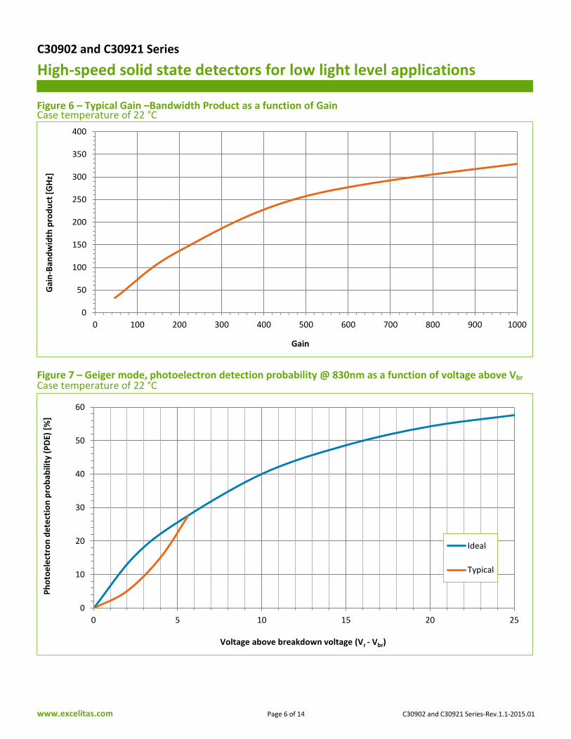
Figure 6 – Typical Gain –Bandwidth Product as a function of Gain Case temperature of 22 °C
Figure 7 – Geiger mode, photoelectron detection probability @ 830nm as a function of voltage above Vbr Case temperature of 22 °C
0
10
20
30
40
50
60
0 5 10 15 20 25
Ph
oto
ele
ctro
n d
ete
ctio
n p
rob
abili
ty (
PD
E) [
%]
Voltage above breakdown voltage (Vr - Vbr)
Ideal
Typical
0
50
100
150
200
250
300
350
400
0 100 200 300 400 500 600 700 800 900 1000
Gai
n-B
and
wid
th p
rod
uct
[G
Hz]
Gain

www.excelitas.com Page 7 of 14 C30902 and C30921 Series-Rev.1.1-2015.01
C30902 and C30921 Series
High-speed solid state detectors for low light level applications
Figure 8 – Load Line for C30921SH in the Geiger mode
Figure 9 – Typical Dark Count vs. Temperature at 5% Photon Detection Efficiency (830nm)
0
50
100
150
200
250
300
350
400
450
500
Dar
k cu
rre
nt
[mA
]
High RL
Low RL
Conducting state (avalanching)
Non-conducting state
(surface dark current only)
Vbr Vr
10
100
1000
10000
-30 -25 -20 -15 -10 -5 0 5 10 15 20 25 30
Dar
k co
un
t [c
ps]
Temperature [°C]

www.excelitas.com Page 8 of 14 C30902 and C30921 Series-Rev.1.1-2015.01
C30902 and C30921 Series
High-speed solid state detectors for low light level applications
Figure 10 – Probability of after-pulse within the next 100ns vs. delay-time in an active quenched circuit (typical for C30902SH and C30921SH at Vbr, at a at case temperature of 22 °C)
Package Drawings (Other packages available upon request)
Figure 11 – C30902EH and C30902SH, reference dimensions shown in mm (inches)
0.1
1
10
100
50 100 150 200 250 300 350
Pro
bab
ility
of
afte
r-p
uls
ing
[%]
Delay Time [ns]

www.excelitas.com Page 9 of 14 C30902 and C30921 Series-Rev.1.1-2015.01
C30902 and C30921 Series
High-speed solid state detectors for low light level applications
Figure 12 – C30921EH and C30921EH, package outline and cutaway of the lightpipe, reference dimensions shown in mm [inches]
Figure 13 – C30902EH-2 and C30902SH-2 reference dimensions shown in mm [inches]

www.excelitas.com Page 10 of 14 C30902 and C30921 Series-Rev.1.1-2015.01
C30902 and C30921 Series
High-speed solid state detectors for low light level applications
Figure 14 – C30902BH, reference dimensions shown in mm
Figure 15– C30902SH-TC/-DTC, TO-66 with flange outline, reference dimensions shown in mm (inches)

www.excelitas.com Page 11 of 14 C30902 and C30921 Series-Rev.1.1-2015.01
C30902 and C30921 Series
High-speed solid state detectors for low light level applications
Figure 16 – Approximate field of view – C30902 and C30921 Series For incident radiation at angles , the photosensitive surface is totally illuminated. For incident radiation at angles , but , the photosensitive surface is partially illuminated
“- TC” and “- DTC” TE Cooled version
TE cooled APD can be used for different reason (Figure 15). Most applications benefits from a -TC (single) or -DTC (dual) version for two reasons:
1. To reduce the thermal noise for very small signal detection as described previously. The -TC version has been design
to operate the APD down to 0C whereas the -DTC version can be operated at -20C when the ambient temperature is
22C. 2. To keep a constant APD temperature no matter the ambient temperature. Because APD breakdown voltage
decreases with a decrease of temperature, the TE cooler allows a single operating voltage. Also, this configuration allows constant APD performance over an extended ambient temperature range.
The thermistor located inside the unit can be used to monitor the APD temperature and can be used to implement a TE cooler feedback loop to keep the APD at a constant temperature or/and to implement a temperature compensation on the APD bias voltage. A proper heat-sink is required to dissipate the heat generated by the APD and the TE cooler.
Custom Designs
Recognizing that different applications have different performance requirements, Excelitas offers a wide range of customization of these APDs to meet your design challenges. Dark count selection, custom device testing and packaging are among many of the application specific solutions available
Geiger mode operation
When biased above the breakdown voltage, an avalanche photodiode will normally conduct a large current. However, if the
current is such that the current is limited to less than a particular value (about 50A for these diodes), the current is unstable and can switch off by itself. The explanation of this behavior is that the number of carriers in the avalanche region at any one time is small and fluctuating wildly. If the number happens to fluctuate to zero, the current must stop. If subsequently remains off until the avalanche pulse is retriggered by a bulk or photo-generated carrier. The “S” versions are selected to have a small bulk-generated dark-current. This makes them suitable for low-noise operation below VBR or photon-counting above Vbr in the Geiger mode. In this so-called Geiger mode, a single photoelectron (or thermally-generated electron) may trigger an avalanche pulse which discharges the photodiode from its reverse operating voltage Vr to a voltage slightly below VBR. The probability of this avalanche occurring is shown in Figure 7 as the “Photoelectron Detection Probability” and as can be seen, it increases with reverse voltage Vr. For a given value of Vr-Vbr, the Photoelectron Detection Probability is independent of Temperature. To determine the Photon Detection Probability, it is necessary to multiply the Photon Detection Probability by the Quantum Efficiency, which is shown in Figure 2. The Quantum Efficiency also is relatively independent of temperature, except near the 1000 nm cut-off. The “S” versions can be used in the Geiger mode using either “passive” or “active” pulse quenching circuits. The advantages and disadvantages of each are discussed below.

www.excelitas.com Page 12 of 14 C30902 and C30921 Series-Rev.1.1-2015.01
C30902 and C30921 Series
High-speed solid state detectors for low light level applications
Passive-Quenching Circuit
The simplest, and in many case a perfectly adequate method of quenching a breakdown pulse, is through the use of a current
limiting load resistor. An example of such a “passive” quenching is shown in Figure 17. The load-line of the circuit is shown in
Figure 8. To be in the conducting state at Vbr two conditions must be met:
1. The Avalanche must have been triggered by either a photoelectron or a bulk-generated electron entering at the
avalanche region of the diode. (Note: holes are inefficient at starting avalanches in silicon.) The probability of an
avalanche being initiated is discussed above.
2. To continue to be in the conducting state a sufficiently large current, called the latching current ILATCH, must be passing
through the device so that there is always an electron or hole in the avalanche region. Typically in the C30902SH and
C30921SH, ILATCH = 50 A. For currents (Vr-Vbr)/RL, much greater than ILATCH, the diode remains conducting. If the
current (Vr-Vbr)/RL, is much less than ILATCH, the diode switches almost immediately to the non-conducting state. If
(Vr-Vbr)/RL is approximately equal to ILATCH, then the diode will switch at an arbitrary time from the conducting to the
non-conducting state depending on when the number of electrons and holes in the avalanche region statistically
fluctuates to zero.
When RL is large, the photodiode is normally conducting, and the operating point is at Vr-IDSRL in the non-conducting state.
Following an avalanche breakdown, the device recharges to the voltage Vr - IDSRL with the time constant RLC, where C is the
total device capacitance including stray capacitance. Using C = 1.6 pF and RL = 200 k a recharge time constant of 0.32 s is
calculated. The rise-time is fast, 5 to 50ns, and decreases as Vr - Vbr increases, and is very dependent on the capacitances of
the load resistors, leads, etc. The jitter at the half-voltage point is typically the same order of magnitude as the rise-time. For
timing purposes where it is important to have minimum jitter, the lowest possible threshold of the rising pulse should be used. Figure 17 – Sample of passive quench circuit
0 200 400 600 800 1000
VR
2 O
utp
ut
volt
age
[ar
b. u
nit
s]
Time [ns]

www.excelitas.com Page 13 of 14 C30902 and C30921 Series-Rev.1.1-2015.01
C30902 and C30921 Series
High-speed solid state detectors for low light level applications
Active-Quenching Circuit
Until the C30902SH is recharged, the probability of detecting another incoming photoelectron is relatively low. To avoid an
excessive dead-time when operating at a large voltage above Vbr, an “actively quenched” circuit can be used. The circuit
temporarily drops the bias voltage for a fraction of a microsecond following the detection of an avalanche discharge. This
delay time allows all electrons and holes to be collected, including most of those temporarily “trapped” at various impurity
sites in the silicon. When the higher voltage is reapplied, there are no electrons in the depletion region to trigger another
avalanche or latch the diode. Recharging can now be very rapid through a small load resistor. Alternatively, the bias voltage
can be maintained but the load resistor is replaced by a transistor which is kept off for a short time after an avalanche, and
then turned on for a period sufficient to recharge the photodiode.
Timing Resolution
For photon counting applications, the time of the TTL triggered pulse after detecting a photon, when plotted on a curve, and
with the FWHM averaged, is the timing resolution or time jitter. The jitter at the half-voltage point is typically the same order
of magnitude as the rise-time. For timing purposes where it is important to have minimum jitter, the lowest possible threshold
of the rising pulse should be used.
After-Pulsing
An after-pulse is an avalanche breakdown pulse which follows, and is induced by, a photon-generated pulse. An after-pulse is
usually caused by one of the approximately 108 carriers which pass through the diode during an avalanche. This electron or
hole is captured and trapped at some impurity site in the silicon, as previously described. When this charge-carrier is liberated,
usually in less than 100 ns but sometimes several milliseconds later, it may start another avalanche. The probability of an
after-pulse occurring more than one microsecond later is typically less than 1% at 2 volts above Vbr, using the circuit shown in
Figure 17.
After-pulsing increases with bias voltage. If it is necessary to reduce after-pulses, it is recommended that one keep Vr-Vbr low,
use an actively-quenched circuit with a long delay-line, or a passively-quenched circuit with a long RLC constant. Stray
capacitances must also be minimized. Electronic gating of the signal can be performed in certain situations. Should after-
pulses be a serious complication in a particular application, operation below Vbr with a good amplifier might be considered.
Dark Current
“S” versions have been selected to have a low dark-count rate. Cooling to -25C can reduce this by a factor of about 50, since
the dependence of dark-count rate on temperature is exponential.
The dark-count increases with voltage following the same curve as the Photoelectron Detection Probability until a voltage
where after-pulsing is responsible for a feedback mechanism which dramatically increases the dark-count rate. This maximum
voltage is circuit dependent, and is not warranted other than the values listed on Table 1. In most cases, with a delay time of
300 ns, the diode can be used effectively at Vr up to Vbr + 25V.
The C30902 should not be forward biased or, when unbiased, exposed to strong illumination. These conditions result in a
greatly enhanced dark-count, which may require up to 24 hours returning to its nominal value.

www.excelitas.com Page 14 of 14 C30902 and C30921 Series-Rev.1.1-2015.01
C30902 and C30921 Series
High-speed solid state detectors for low light level applications
RoHS Compliance
The C30902 and C30921 series of avalanche photodiodes are designed and built to be fully compliant with the European Union
Directive 2011/65/EU – Restriction of the use of certain Hazardous Substances (RoHS) in Electrical and Electronic equipment.
Warranty
A standard 12-month warranty following shipment applies. Any warranty is null and void if the photodiode window has been
opened.
About Excelitas Technologies
Excelitas Technologies is a global technology leader focused on delivering innovative, customized solutions to meet the
lighting, detection and other high-performance technology needs of OEM customers.
Excelitas has a long and rich history of serving our OEM customer base with optoelectronic sensors and modules for more than
45 years beginning with PerkinElmer, EG&G, and RCA. The constant throughout has been our innovation and commitment to
delivering the highest quality solutions to our customers worldwide.
From aerospace and defense to analytical instrumentation, clinical diagnostics, medical, industrial, and safety and security
applications, Excelitas Technologies is committed to enabling our customers' success in their specialty end-markets. Excelitas
Technologies has approximately 3,000 employees in North America, Europe and Asia, serving customers across the world.
Excelitas Technologies 22001 Dumberry Road Vaudreuil-Dorion, Quebec Canada J7V 8P7 Telephone: (+1) 450 424 3300 Toll-free: (+1) 800 775 6786 Fax: (+1) 450 424 3345 [email protected]
Excelitas Technologies GmbH & Co. KG Wenzel-Jaksch-Str. 31 D-65199 Wiesbaden Germany Telephone: (+49) 611 492 430 Fax: (+49) 611 492 165 [email protected]
Excelitas Technologies Singapore, Pte. Ltd. 8 Tractor Road Singapore 627969 Telephone: (+65) 6775 2022 (Main number) Telephone: (+65) 6770 4366 (Customer Service) Fax: (+65) 6778-1752 [email protected]
For a complete listing of our global offices, visit www.excelitas.com/locations © 2014 Excelitas Technologies Corp. All rights reserved. The Excelitas logo and design are registered trademarks of Excelitas Technologies Corp. All other trademarks not owned by Excelitas Technologies or its subsidiaries that are depicted herein are the property of their respective owners. Excelitas reserves the right to change this document at any time without notice and disclaims liability for editorial, pictorial or typographical errors.