blue and uv semiconductor lasers - … · blue and uv semiconductor lasers 1267 difficult to...
TRANSCRIPT

See discussions, stats, and author profiles for this publication at: https://www.researchgate.net/publication/251259826
Blue and UV Semiconductor Lasers
Article · April 2006
CITATIONS
6
READS
64
6 authors, including:
Some of the authors of this publication are also working on these related projects:
QuantREIonics: Hysteretic photochromic switching of Eu-Mg defects in GaN View project
Mechanical Properties of Glasses View project
Stanislaw Krukowski
Warsaw University of Technology
100 PUBLICATIONS 1,210 CITATIONS
SEE PROFILE
Piotr Perlin
Polish Academy of Sciences
356 PUBLICATIONS 6,039 CITATIONS
SEE PROFILE
Michal Bockowski
Instytut Wysokich Ciśnień
286 PUBLICATIONS 3,425 CITATIONS
SEE PROFILE
All content following this page was uploaded by Michal Bockowski on 29 March 2014.
The user has requested enhancement of the downloaded file.
Vol. 37 (2006) ACTA PHYSICA POLONICA B No 4
BLUE AND UV SEMICONDUCTOR LASERS∗
S. Krukowski, C. Skierbiszewski, P. Perlin, M. Leszczynski,
M. Bockowski, S. Porowski
Institute of High Pressure Physics, Polish Academy of SciencesSokołowska 29/37, 01-142 Warsaw, Poland
(Received March 28, 2006)
Despite many technological difficulties the group III nitrides: GaN,AlN and InN and their alloys are primary candidates for electro-opticalcoherent light sources. In the recent years the research and technology ofthe nitride based continuous wave (CW) laser diodes (LDs) led to creationof blue-violet coherent light sources of power up to 200 mW. The progresshas been attained by using various ways to attack the main obstacles in thetechnology of these devices such as insufficient size of high quality latticematched substrates, low p-doping efficiency of Mg acceptor, poor contact top-type semiconductor and low efficiency of radiative recombination. Thetwo different approaches were used to overcome the substrate problem:hetero-epitaxy and homoepitaxy. Homoepitaxy used high pressure GaNhigh quality crystals. Heteroepitaxy used sapphire, SiC or GaAs substratesand very sophisticated techniques of reduction of the dislocation density.The low p-doping efficiency by using Mg acceptor is related to creationof Mg–H complexes due to hydrogen presence during the growth of laserdiode quantum structures. In addition, Mg acceptor has low efficiencydue to its high energy. High Mg concentrations can be obtained by usingeither MOCVD or ammonia source MBE growth. An alternative route is touse hydrogen-free plasma activated MBE (PA-MBE) method. The recentadvances and the prospects of both approaches will be discussed. SolidAlGaInN solution offers a possibility to cover wide spectral range, startingfrom near UV to blue, green and red. Arsenide based laser diodes (LDs)are efficient coherent red light sources. Therefore, nitride based LDs areconsidered to be devices of choice for green, blue and UV spectral range.So far only blue and violet laser has been realized. The progress towardgreen and UV lasers is far less spectacular. The results in all these areasand future prospects will be discussed.
PACS numbers: 81.05.Ea, 68.55.Ac, 81.15.–z, 42.55.Px
∗ Presented at the PLC2005 Workshop, 5–8 September 2005, Kazimierz, Poland.
(1265)
1266 S. Krukowski et al.
1. Introduction
GaN, AlN and InN and their solid solutions became the materials ofchoice for short-wavelength optoelectronics only recently [1]. These com-pounds were selected not only due to their wide direct energy gaps, coveringthe whole visible spectrum and near UV range, but also due to their ex-cellent physical properties such as hardness, physical and chemical stability.Therefore, these materials become a prime object of interest of engineersdesigning optoelectronic devices that have high energy density in the activeregions of the devices.
GaN was first synthesized in the early thirties [2], but its applicationin electronics was hampered by extreme difficulties of growing it in singlecrystalline form. The latter fact arises from the thermodynamic propertiesof GaN which has very high melting temperature — 2220C that is accom-panied by high equilibrium nitrogen pressure close to 60 000 bar [3]. Atpresent the large size substrate quality GaN crystals are obtained by HighNitrogen Pressure Solution Growth (HNPSG) method [4,5]. The size of thecrystal reach 2 cm and their thickness is about 100 µm, which allows themanufacturing of high power Laser Diodes (LDs). The production output issufficient for covering professional application of high power devices on theinternational scale.
This option is a solution for high power professional devices. Anotherroute to large scale manufacturing of blue laser diodes was proposed [6–9]for mass production. The two different methods are based on application offoreign substrates, such as sapphire, SiC or GaAs. In the first method, calledepitaxial lateral overgrowth (ELOG), GaN template layers are deposited inthe standard way, by MOVPE or HVPE method, on the surface of highquality substrate. Then an important step is deposition of the mask, usuallySiO2 [6,8] or TiN [7] which covers the most of the surface. Subsequent growthof GaN allows to obtain thick GaN substrate with the dislocation density ofabout 107 cm−2.
The alternative method, called hetero-epitaxial lateral overgrowth(HELO) relies on the deposition of the mask directly on the foreign sub-strate [9]. The process omits the template growth. The thick GaN layer isthen deposited directly on the substrate. The early stage of the growth ischaracterized by the independent growth of GaN islands. Afterwards theGaN islands coalesce and the mirror-like GaN surface is developed.
Depending on the growth method, the GaN layer can be either removedfrom the substrate or it can be used directly to growth of laser quantumstructures. The removed GaN layer creates so called free-standing GaN sub-strate which can be used for the deposition of laser structures. The process is
Blue and UV Semiconductor Lasers 1267
difficult to control, but it provides large area (two inch) GaN wafers. Thesewafers have at present about dislocation density of 106–107 cm−2, which issufficient as substrates for the manufacturing of small number of relativelyhigh power blue LDs [6–9]. However, the issue whether this method can beused for mass production of low power blue LDs remains to be solved. Sim-ilarly the more difficult problem of high quality substrates for high powerblue, green and UV LDs is open.
The HVPE growth of GaN on sapphire substrate was used already in60-ties to obtain first high quality GaN layers, which were used to determinethe physical properties of gallium nitride [10–13]. It was established thatGaN layers have high concentration of electrons. The attempts to dope forp-type were not successful, which was the largest obstacle to highly efficientoptoelectronic devices. The results of doping were so disappointing thatlarge scale efforts to obtain GaN based light emitting diodes (LEDs) wereabandoned in 70-ties.
The comeback of nitrides occurred in 1989 thanks to Japanese scien-tists Amano and Akasaki who discovered the method of activation of Mgacceptors by electron irradiation and obtained first p-type GaN layers [14].Later Nakamura discovered an industrially important method of activationof Mg acceptors by annealing in hydrogen-free atmosphere [15]. Nakamuraimproved considerably MOVPE technique to grow nitride (GaN, InGaN)layers on sapphire substrates by introducing low temperature nitride (AlNor GaN) buffer layers and annealing before the second growth stage. Fromthis time on the technology of mass production of high brightness blue andgreen light emitting diodes (LEDs) was developed with the use of sapphiresubstrates [1].
It has to be noted, that the technology for laser diodes is far more de-manding with respect to crystallographic quality of the substrates and thedeposited layers. Despite great technical difficulties, Nakamura obtained thefirst blue LD in 1996 [16]. The result was obtained by considerable improve-ment of the crystallographic quality of the MOVPE grown nitride layersusing epitaxial lateral overgrowth (ELOG) technique [1]. Since then, theprogress in this technology led to the creation of the blue laser which wascommercialized. At present 50 mW continuous wave (CW) blue lasers areoffered to the market. The progress has been, however, much slower thanexpected [17] and the mass production of blue laser diodes has not yet beenachieved.
The progress in the related segments of green and UV devices is evenslower. Superbright green LEDs were also developed by Nakamura andoffered to the market as soon as the blue ones. In contrast to that, greenLDs have not been obtained. The poor result in the green laser challengeis related to the difficulty in growing high quality In-rich structures by the
1268 S. Krukowski et al.
MOVPE technique [28]. This involves serious technical difficulties and thegreen nitride based laser has not been created so far.
The progress in the technology of UV devices has been even slower. Itwas related to the poor efficiency of quantum well structures grown withoutindium. It has to be noted that the role of indium, dramatically increasinglight emission efficiency, has not been elucidated. The AlGaN structurestypically used for UV emitters are less effective emitters. Therefore, bothUV LEDs and LDs are far behind their blue/violet counterparts.
An important aspect of the technology of all nitride based devices is p-type doping. Magnesium is still the only effective acceptor. Relatively highionization energy (200 meV in case of GaN) limits the fraction of ionizedacceptors to 1% at room temperature. This problem is aggravated by lowmobility of holes in nitride layers. Together it deteriorates electrical prop-erties of GaN and AlGaN layers and electric contact to p-type. This causesintensive heat generation, which is a serious problem for high power devices.
Despite these problems, the heteroepitaxial nitride technologies pro-gressed fast and at present the highly efficient blue LEDs are produced atrelatively low cost. The later stage directed to laser technology has been lesssuccessful. As the result, low cost blue/violet LDs were not marketed. Thishas created a new chance to homoepitaxial technology. The homoepitaxywas developing slowly at early stage because of the difficulties in obtain-ing large, high quality GaN crystals which could be used as substrates forepitaxial deposition of multilayer quantum structures necessary for devices.This is a direct consequence of thermodynamic properties of GaN [5] (andalso AlN [19]), in particular, its melting conditions which are so extreme,that the application of the common growth methods from stoichiometricliquids is technically impossible. The most successful method of growingthe dislocation-free GaN crystals so far is the growth of GaN under highpressure of nitrogen.
High pressure (HP) grown low dislocation density GaN crystals wereused as substrates for MOVPE and MBE epitaxial deposition. The stan-dard blue/violet laser diodes obtained by these methods in the Institute ofHigh Pressure Physics of PAS (IHPP PAS) have the comparable parameters.The Plasma Assisted Molecular Beam Epitaxy (PA-MBE) technique offersunique possibility to grow laser structures in hydrogen-free atmosphere. Alsothe new structures for green and UV LEDs were successfully grown. It isexpected that in the near future, both green and UV laser diodes could bedeveloped by using PA-MBE technique. The results and the prospects forthe near future will be described in this paper.
Blue and UV Semiconductor Lasers 1269
2. High pressure crystallization of GaN
2.1. Thermodynamic properties of GaN-Ga-N2 system
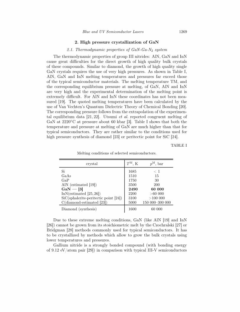
The thermodynamic properties of group III nitrides: AlN, GaN and InNcause great difficulties for the direct growth of high quality bulk crystalsof these compounds. Similar to diamond, the growth of high quality singleGaN crystals requires the use of very high pressures. As shown in Table I,AlN, GaN and InN melting temperatures and pressures far exceed thoseof the typical semiconductor materials. The melting temperature TM, andthe corresponding equilibrium pressure at melting, of GaN, AlN and InNare very high and the experimental determination of the melting point isextremely difficult. For AlN and InN these coordinates has not been mea-sured [19]. The quoted melting temperatures have been calculated by theuse of Van Vechten’s Quantum Dielectric Theory of Chemical Bonding [20].The corresponding pressure follows from the extrapolation of the experimen-tal equilibrium data [21, 22]. Utsumi et al. reported congruent melting ofGaN at 2220C at pressure about 60 kbar [3]. Table I shows that both thetemperature and pressure at melting of GaN are much higher than that fortypical semiconductors. They are rather similar to the conditions used forhigh pressure synthesis of diamond [23] or peritectic point for SiC [24].
TABLE I
Melting conditions of selected semiconductors.
crystal T M, K pM, bar
Si 1685 < 1GaAs 1510 15GaP 1750 30AlN (estimated [19]) 3500 200GaN — [3] 2490 60 000InN(estimated [25, 26]) 2200 >60 000SiC(sphalerite-peritectic point [24]) 3100 >100 000C(diamond-estimated [23]) 5000 150 000–300 000
Diamond (synthesis) 1600 60 000
Due to these extreme melting conditions, GaN (like AlN [19] and InN[26]) cannot be grown from its stoichiometric melt by the Czochralski [27] orBridgman [28] methods commonly used for typical semiconductors. It hasto be crystallized by methods which allow to grow the bulk crystals usinglower temperatures and pressures.
Gallium nitride is a strongly bonded compound (with bonding energyof 9.12 eV/atom pair [29]) in comparison with typical III-V semiconductors
1270 S. Krukowski et al.
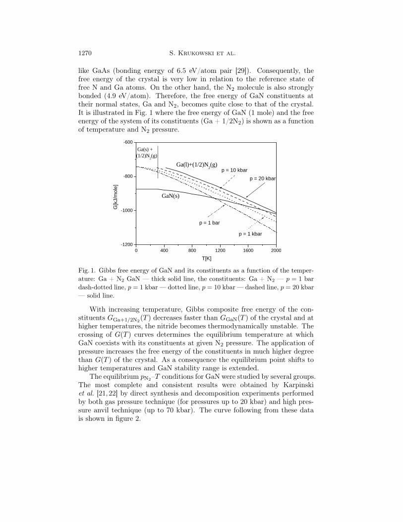
like GaAs (bonding energy of 6.5 eV/atom pair [29]). Consequently, thefree energy of the crystal is very low in relation to the reference state offree N and Ga atoms. On the other hand, the N2 molecule is also stronglybonded (4.9 eV/atom). Therefore, the free energy of GaN constituents attheir normal states, Ga and N2, becomes quite close to that of the crystal.It is illustrated in Fig. 1 where the free energy of GaN (1 mole) and the freeenergy of the system of its constituents (Ga + 1/2N2) is shown as a functionof temperature and N2 pressure.
0 400 800 1200 1600 2000-1200
-1000
-800
-600
p = 20 kbar
p = 10 kbar
p = 1 bar
p = 1 kbar
Ga(s) +(1/2)N
2(g)
Ga(l)+(1/2)N2(g)
GaN(s)
G[k
J/m
ole]
T[K]
Fig. 1. Gibbs free energy of GaN and its constituents as a function of the temper-ature: Ga + N2 GaN — thick solid line, the constituents: Ga + N2 — p = 1 bardash-dotted line, p = 1 kbar — dotted line, p = 10 kbar — dashed line, p = 20 kbar— solid line.
With increasing temperature, Gibbs composite free energy of the con-stituents GGa+1/2N2
(T ) decreases faster than GGaN(T ) of the crystal and athigher temperatures, the nitride becomes thermodynamically unstable. Thecrossing of G(T ) curves determines the equilibrium temperature at whichGaN coexists with its constituents at given N2 pressure. The application ofpressure increases the free energy of the constituents in much higher degreethan G(T ) of the crystal. As a consequence the equilibrium point shifts tohigher temperatures and GaN stability range is extended.
The equilibrium pN2–T conditions for GaN were studied by several groups.
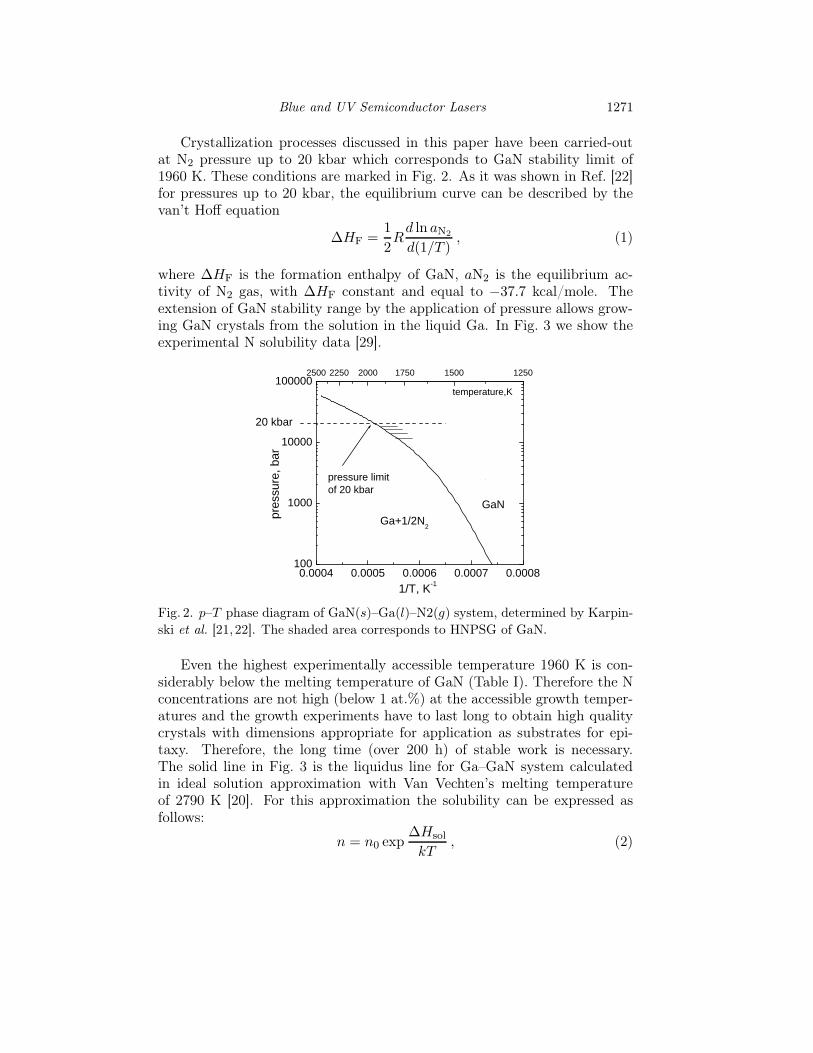
The most complete and consistent results were obtained by Karpinskiet al. [21, 22] by direct synthesis and decomposition experiments performedby both gas pressure technique (for pressures up to 20 kbar) and high pres-sure anvil technique (up to 70 kbar). The curve following from these datais shown in figure 2.
Blue and UV Semiconductor Lasers 1271
Crystallization processes discussed in this paper have been carried-outat N2 pressure up to 20 kbar which corresponds to GaN stability limit of1960 K. These conditions are marked in Fig. 2. As it was shown in Ref. [22]for pressures up to 20 kbar, the equilibrium curve can be described by thevan’t Hoff equation
∆HF =1
2R
d ln aN2
d(1/T ), (1)
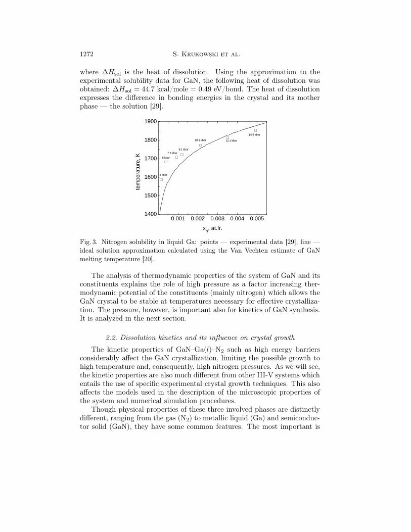
where ∆HF is the formation enthalpy of GaN, aN2 is the equilibrium ac-tivity of N2 gas, with ∆HF constant and equal to −37.7 kcal/mole. Theextension of GaN stability range by the application of pressure allows grow-ing GaN crystals from the solution in the liquid Ga. In Fig. 3 we show theexperimental N solubility data [29].
0.0004 0.0005 0.0006 0.0007 0.0008100
1000
10000
100000
20 kbar
pressure limitof 20 kbar
GaN
Ga+1/2N2
temperature,K
pres
sure
, bar
1/T, K-1
2500 2250 2000 1750 1500 1250
Fig. 2. p–T phase diagram of GaN(s)–Ga(l)–N2(g) system, determined by Karpin-ski et al. [21, 22]. The shaded area corresponds to HNPSG of GaN.
Even the highest experimentally accessible temperature 1960 K is con-siderably below the melting temperature of GaN (Table I). Therefore the Nconcentrations are not high (below 1 at.%) at the accessible growth temper-atures and the growth experiments have to last long to obtain high qualitycrystals with dimensions appropriate for application as substrates for epi-taxy. Therefore, the long time (over 200 h) of stable work is necessary.The solid line in Fig. 3 is the liquidus line for Ga–GaN system calculatedin ideal solution approximation with Van Vechten’s melting temperatureof 2790 K [20]. For this approximation the solubility can be expressed asfollows:
n = n0 exp∆Hsol
kT, (2)
1272 S. Krukowski et al.
where ∆Hsol is the heat of dissolution. Using the approximation to theexperimental solubility data for GaN, the following heat of dissolution wasobtained: ∆Hsol = 44.7 kcal/mole = 0.49 eV/bond. The heat of dissolutionexpresses the difference in bonding energies in the crystal and its motherphase — the solution [29].
0.001 0.002 0.003 0.004 0.0051400
1500
1600
1700
1800
1900
3 kbar
6 kbar
7.3 kbar8.1 kbar
10.1 kbar 12.1 kbar
14.5 kbarte
mpe
ratu
re, K
xN, at.fr.
Fig. 3. Nitrogen solubility in liquid Ga: points — experimental data [29], line —ideal solution approximation calculated using the Van Vechten estimate of GaNmelting temperature [20].
The analysis of thermodynamic properties of the system of GaN and itsconstituents explains the role of high pressure as a factor increasing ther-modynamic potential of the constituents (mainly nitrogen) which allows theGaN crystal to be stable at temperatures necessary for effective crystalliza-tion. The pressure, however, is important also for kinetics of GaN synthesis.It is analyzed in the next section.
2.2. Dissolution kinetics and its influence on crystal growth
The kinetic properties of GaN–Ga(l)–N2 such as high energy barriersconsiderably affect the GaN crystallization, limiting the possible growth tohigh temperature and, consequently, high nitrogen pressures. As we will see,the kinetic properties are also much different from other III-V systems whichentails the use of specific experimental crystal growth techniques. This alsoaffects the models used in the description of the microscopic properties ofthe system and numerical simulation procedures.
Though physical properties of these three involved phases are distinctlydifferent, ranging from the gas (N2) to metallic liquid (Ga) and semiconduc-tor solid (GaN), they have some common features. The most important is
Blue and UV Semiconductor Lasers 1273
that the atoms in all three phases are extremely strongly bonded. Molecularnitrogen is the strongest bonded diatomic molecule in nature, the dissocia-tion energy of N2 molecule is 9.76 eV [29]. Gallium liquid is characterized byhigh enthalpy of evaporation 271 kJ/mole (2.81 eV/atom) which is reflectedby the critical temperature, close to 4000 K [30, 31]. Similarly, solid GaNis strongly bonded, with the energy 9.12 eV/atom pair, which leads to highmelting temperature, close to 2500 K [3].
GaN synthesis from its constituents proceeds via dissolution of nitrogenin liquid gallium, transport of nitrogen to the cold part of the liquid andthe growth from the solution. These stages include dissociation of the N2
molecule which ought to be characterized by high energy barrier. It is ex-pected that the dissociation process involve significant change of the bindingenergy of the molecule, highly exceeding the typical thermal motion energieswhich, for the GaN growth conditions, are close to 0.15 eV.
It is likely that the dissociation occurs during the adsorption of the N2
molecules on liquid Ga surface. This possibility was investigated by solvingquantum mechanical many body problem with the use of density functionalmethod (DFT) formulation [32]. Since thermal motion of the Ga atoms playsa minor role, Born–Oppenheimer approximation can be used. An infiniteGa surface can be simulated by a finite cluster of Ga atoms [33, 34].
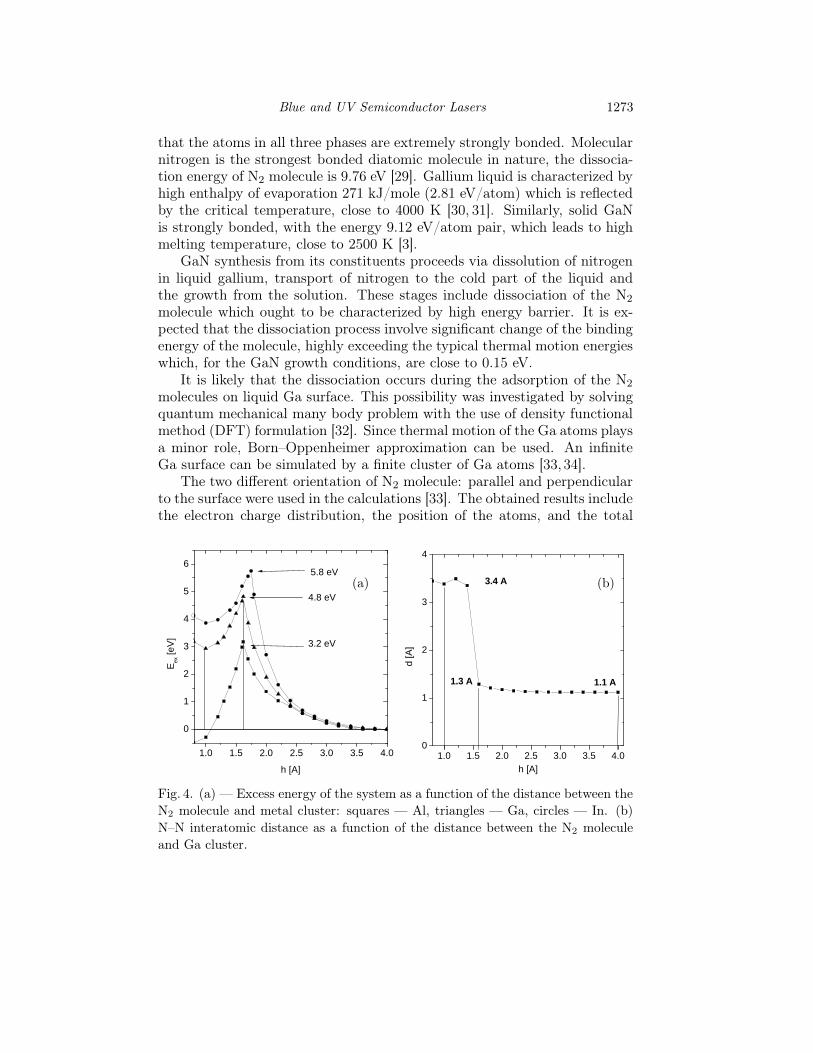
The two different orientation of N2 molecule: parallel and perpendicularto the surface were used in the calculations [33]. The obtained results includethe electron charge distribution, the position of the atoms, and the total
1.0 1.5 2.0 2.5 3.0 3.5 4.0
0
1
2
3
4
5
6
3.2 eV
4.8 eV
5.8 eV
Eex
[eV
]
h [A]
1.0 1.5 2.0 2.5 3.0 3.5 4.00
1
2
3
4
3.4 A
1.1 A1.3 A
d [A
]
h [A]
(a) (b)
Fig. 4. (a) — Excess energy of the system as a function of the distance between theN2 molecule and metal cluster: squares — Al, triangles — Ga, circles — In. (b)N–N interatomic distance as a function of the distance between the N2 moleculeand Ga cluster.
1274 S. Krukowski et al.
energies of the system. In Fig. 4(a) we present the change of the totalenergy of the system as a function of the distance between the Ga surfaceand the N2 molecule. In these data the parallel orientation of the moleculeto the surface has been used. The interaction is negligible for distanceshigher than 4 Å for which the excess energy zero level is adopted. For closerdistances the energy increases sharply to reach 4.8 eV for d = 1.6 Å andthen sharply decreases. As shown in Fig. 4(b), the excess energy increaseoccurs when the N–N distance is only slightly increased whereas the decreaseoccurs after the N–N distance increased suddenly to more than 3.2 Å. Thisdramatic change indicates that at the distance 1.6 Å, the dissociation of theN2 molecule takes place.
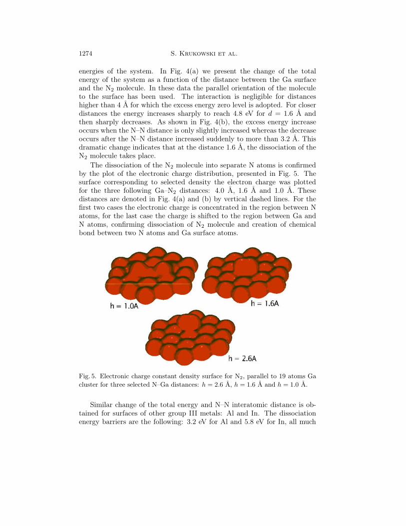
The dissociation of the N2 molecule into separate N atoms is confirmedby the plot of the electronic charge distribution, presented in Fig. 5. Thesurface corresponding to selected density the electron charge was plottedfor the three following Ga–N2 distances: 4.0 Å, 1.6 Å and 1.0 Å. Thesedistances are denoted in Fig. 4(a) and (b) by vertical dashed lines. For thefirst two cases the electronic charge is concentrated in the region between Natoms, for the last case the charge is shifted to the region between Ga andN atoms, confirming dissociation of N2 molecule and creation of chemicalbond between two N atoms and Ga surface atoms.
Fig. 5. Electronic charge constant density surface for N2, parallel to 19 atoms Gacluster for three selected N–Ga distances: h = 2.6 Å, h = 1.6 Å and h = 1.0 Å.
Similar change of the total energy and N–N interatomic distance is ob-tained for surfaces of other group III metals: Al and In. The dissociationenergy barriers are the following: 3.2 eV for Al and 5.8 eV for In, all much
Blue and UV Semiconductor Lasers 1275
lower than the N2 dissociation energy, which indicates strong catalytic in-fluence of group III metal surface.
The calculation of the interaction of the N2 molecule, oriented perpendic-ular to Ga surface also confirmed the dissociation of the molecule. Generally,the energy barriers are much lower for this orientation: 3.0 eV for Al, 3.4 eVfor Ga and 3.6 eV for In. Since the interatomic distances are much largerfor a In cluster, one can expect that the energy barrier for Al and Ga arerelatively overestimated due to larger stiffness of these two clusters.
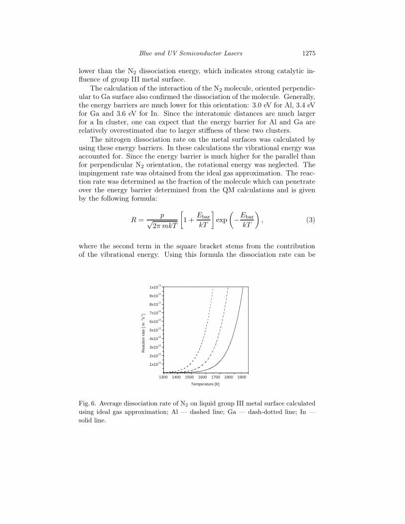
The nitrogen dissociation rate on the metal surfaces was calculated byusing these energy barriers. In these calculations the vibrational energy wasaccounted for. Since the energy barrier is much higher for the parallel thanfor perpendicular N2 orientation, the rotational energy was neglected. Theimpingement rate was obtained from the ideal gas approximation. The reac-tion rate was determined as the fraction of the molecule which can penetrateover the energy barrier determined from the QM calculations and is givenby the following formula:
R =p√
2π mkT
[
1 +Ebar
kT
]
exp
(
−Ebar
kT
)
, (3)
where the second term in the square bracket stems from the contributionof the vibrational energy. Using this formula the dissociation rate can be
1300 1400 1500 1600 1700 1800 1900
1x10 22
2x10 22
3x10 22
4x10 22
5x10 22
6x10 22
7x10 22
8x10 22
9x10 22
1x10 23
Rea
ctio
n ra
te [
m -2
s -1 ]
Temperature [K]
Fig. 6. Average dissociation rate of N2 on liquid group III metal surface calculatedusing ideal gas approximation; Al — dashed line; Ga — dash-dotted line; In —solid line.
1276 S. Krukowski et al.
calculated for given temperature and pressure of the nitrogen. The temper-ature dependence of the nitrogen dissociation reaction rate for Ga, Al andsurfaces, for the gas pressure 20 kbar is presented in Fig. 6.
The nitrogen dissolved in the hot end Ga surface is transported intothe cold part of the liquid by convection and diffusion. There the GaNgrowth proceeds via three main stages. The initial stage is a heterogeneousnucleation of GaN on the Ga surface. During the second stage the growthof numerous GaN crystals and separation of the dominant growth centersoccurs. And the final stage is the growth of small number of single crystalsin the supersaturated solution of N in liquid Ga. The last stage determinesthe results of the crystallization process.
2.3. Crystal growth of GaN by high nitrogen pressure solution(HNPSG) method — experimental
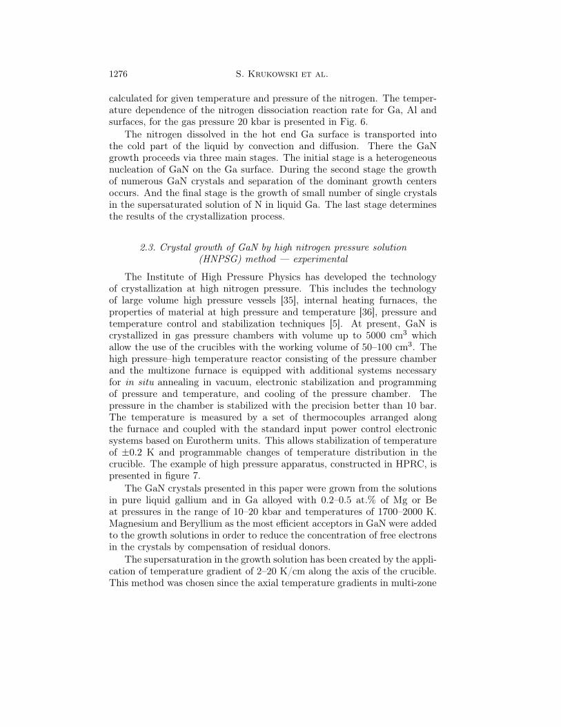
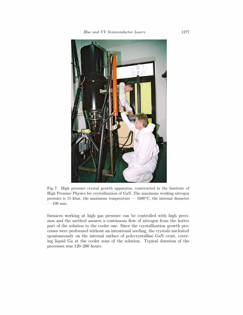
The Institute of High Pressure Physics has developed the technologyof crystallization at high nitrogen pressure. This includes the technologyof large volume high pressure vessels [35], internal heating furnaces, theproperties of material at high pressure and temperature [36], pressure andtemperature control and stabilization techniques [5]. At present, GaN iscrystallized in gas pressure chambers with volume up to 5000 cm3 whichallow the use of the crucibles with the working volume of 50–100 cm3. Thehigh pressure–high temperature reactor consisting of the pressure chamberand the multizone furnace is equipped with additional systems necessaryfor in situ annealing in vacuum, electronic stabilization and programmingof pressure and temperature, and cooling of the pressure chamber. Thepressure in the chamber is stabilized with the precision better than 10 bar.The temperature is measured by a set of thermocouples arranged alongthe furnace and coupled with the standard input power control electronicsystems based on Eurotherm units. This allows stabilization of temperatureof ±0.2 K and programmable changes of temperature distribution in thecrucible. The example of high pressure apparatus, constructed in HPRC, ispresented in figure 7.
The GaN crystals presented in this paper were grown from the solutionsin pure liquid gallium and in Ga alloyed with 0.2–0.5 at.% of Mg or Beat pressures in the range of 10–20 kbar and temperatures of 1700–2000 K.Magnesium and Beryllium as the most efficient acceptors in GaN were addedto the growth solutions in order to reduce the concentration of free electronsin the crystals by compensation of residual donors.
The supersaturation in the growth solution has been created by the appli-cation of temperature gradient of 2–20 K/cm along the axis of the crucible.This method was chosen since the axial temperature gradients in multi-zone
Blue and UV Semiconductor Lasers 1277
Fig. 7. High pressure crystal growth apparatus, constructed in the Institute ofHigh Pressure Physics for crystallization of GaN. The maximum working nitrogenpressure is 15 kbar, the maximum temperature — 1600C, the internal diameter— 100 mm.
furnaces working at high gas pressure can be controlled with high preci-sion and the method assures a continuous flow of nitrogen from the hotterpart of the solution to the cooler one. Since the crystallization growth pro-cesses were performed without an intentional seeding, the crystals nucleatedspontaneously on the internal surface of polycrystalline GaN crust, cover-ing liquid Ga at the cooler zone of the solution. Typical duration of theprocesses was 120–200 hours.
1278 S. Krukowski et al.
The slow cooling at isothermal conditions was not applied due to smallconcentrations of nitrogen in the liquid gallium (Fig. 3). The crystallizationat constant temperature, at N2 overpressure was not applied as well sincethen the crystallization can occur only on the Ga surface and stops if thewhole surface covers with GaN.
2.4. GaN single crystals
2.4.1. Crystals grown without intentional seeding
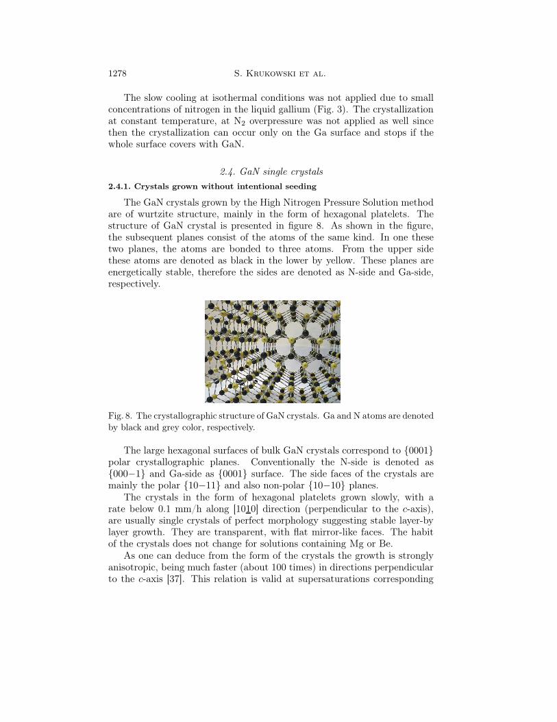
The GaN crystals grown by the High Nitrogen Pressure Solution methodare of wurtzite structure, mainly in the form of hexagonal platelets. Thestructure of GaN crystal is presented in figure 8. As shown in the figure,the subsequent planes consist of the atoms of the same kind. In one thesetwo planes, the atoms are bonded to three atoms. From the upper sidethese atoms are denoted as black in the lower by yellow. These planes areenergetically stable, therefore the sides are denoted as N-side and Ga-side,respectively.
Fig. 8. The crystallographic structure of GaN crystals. Ga and N atoms are denotedby black and grey color, respectively.
The large hexagonal surfaces of bulk GaN crystals correspond to 0001polar crystallographic planes. Conventionally the N-side is denoted as000−1 and Ga-side as 0001 surface. The side faces of the crystals aremainly the polar 10−11 and also non-polar 10−10 planes.
The crystals in the form of hexagonal platelets grown slowly, with arate below 0.1 mm/h along [1010] direction (perpendicular to the c-axis),are usually single crystals of perfect morphology suggesting stable layer-bylayer growth. They are transparent, with flat mirror-like faces. The habitof the crystals does not change for solutions containing Mg or Be.
As one can deduce from the form of the crystals the growth is stronglyanisotropic, being much faster (about 100 times) in directions perpendicularto the c-axis [37]. This relation is valid at supersaturations corresponding

Blue and UV Semiconductor Lasers 1279
(0001)
(000-1)
10-11
10-10
-101-1
Fig. 9. GaN crystals grown using high nitrogen pressure. The distances betweengrid lines correspond to 1 mm. The schematic cross-section of the hexagonalplatelet is shown in the upper part.
to the average growth rate in 10−10 directions of 0.05–0.1 mm/h. As willbe shown in the next section, the domination of the growth in the planeperpendicular to the c-axis is typical to relatively low supersaturations.
As it is shown in the next section, high supersaturations enhance thegrowth into c-direction which, unfortunately, leads to the unstable needle-like forms. The supersaturation in the growth solution is determined mainlyby the growth temperature, temperature gradients, mass transport mecha-nisms in gallium and also by the local surrounding for a particular crystal(i.e. the presence of neighboring crystals). For crystallization of large GaNcrystals, it is crucial to control the supersaturation in order to avoid ac-celeration of the growth near edges and corners of the growing crystal. Ifsupersaturation is too high, the edge nucleation on hexagonal faces of GaNplatelets is often observed, which is the first step to the unstable growth onthat faces.
The polarity of the crystal surfaces was identified by etching in hot alkaliwater solutions since the Ga-polar surface is inert to etching whereas theN-polar one etches well for both types of crystals. The method was calibratedby CBED [38,39] and XPS [40] measurements.
2.4.2. Crystals grown without intentional seeding — 2-d nucleation controlled
growth rate
Due to high bonding energy and crystallographic structure of main sur-faces, the growth of GaN crystals is strongly anisotropic. This is reflected inthe shape of GaN crystals which is hexagonal platelet or hexagonal needle.
1280 S. Krukowski et al.
It follows from that observation that for the case of plate-like crystals, thegrowth rates are the fastest for 1011 and 1011, slower for 1010 andthe slowest for 0001 and 0001 surfaces. In case of the needle-like crys-tals the velocity ordering is reversed. For both cases the flat faces of GaNcrystals indicate that they grow by 2-d or layer-by-layer mechanism.
One of the most efficient growth centers are screw dislocations. Sincein the GaN wurtzite structure screw dislocations have much higher energiesthan edge dislocation, their fraction in total dislocation density is small. Incase of the growth of good quality GaN crystals, the role of screw dislocationis negligible.
In absence of the screw dislocation the morphological properties of GaNgrowth results from the competition between the nucleation and completionof new layers. These two processes have different size dependence. At stablethermodynamic conditions at the surface the nucleation rate is proportionalto the surface whereas the completion rate is inversely proportional to thedominant linear size of the surface. In most cases it is proportional tothe inverse of the square root of the surface. Hence one can expect that,for some cases, the transition from the nucleation to completion controlledgrowth occurs.
Growth controlled by 2-d nucleation is morphologically stable. In mostcases the surfaces 10−10 and 000−1 are atomically flat with severalsteps. The growth rate can be assessed using Becker–Doring nucleationlaw [41]. The rate is strongly dependent on supersaturation at the surface.Assuming that the edge energy is due to 2 broken bonds per atom site andusing dissolution energy as the broken bond energy difference, the rate canbe expressed as a function of the supersaturation [23]. For experimentalgrowth rates, these calculations give 48% supersaturation at the growthzone, which is in good agreement with the estimation obtained from thetemperature difference in the crucible and the x–T phase diagram [23].
In case of the other GaN faces the surface is not so flat. This is typicalfor the growth controlled by step flow where nucleation rate is so fast thatit allows to obtain numerous 2-d nuclei at various parts of the surface beforethe layer is completed. This can be caused either by the step pinning dueto the kink poisoning by the impurities or by extremely fast nucleationresulting from relatively high supersaturation. Also the presence of screwdislocation growth centers can cause similar effect. The resulting growthis much faster in some part of the surface leading to the creation of hilland valley morphology and the transition to the morphologically unstableforms. This type of the growth is observed sometimes in the growth on0001 surfaces.
The relative rates on the various faces of GaN crystals can be estimatedby using 2-d nucleation controlled growth. In the following we assume that
Blue and UV Semiconductor Lasers 1281
the change of supersaturation on the face is negligible. This is a good ap-proximation due to relatively small size of the crystal and very low growthrates. Therefore, the diffusion in the liquid homogenizes the concentrationrelatively fast and the growth proceeds in the uniform, stationary concen-tration.
The 2-d growth rate can be expressed by using Becker–Doring nucleationformula [41]. The nucleation rate is treated as thermally activated processwith the energy barrier calculated as the difference of the volume and surfaceterms. The total rate for unit of the surface area I is expressed as the averagefrequency of attaching a molecule ν at the nucleus circumference and theprobability of overcoming the energy barrier ∆G∗:
I = xsqν exp
(
−∆G∗
kT
)
, (4)
where xs is the concentration of the nitrogen in the solution at the GaNsurface, q is the number of the sites at the circumference of the 2-d nucleus.
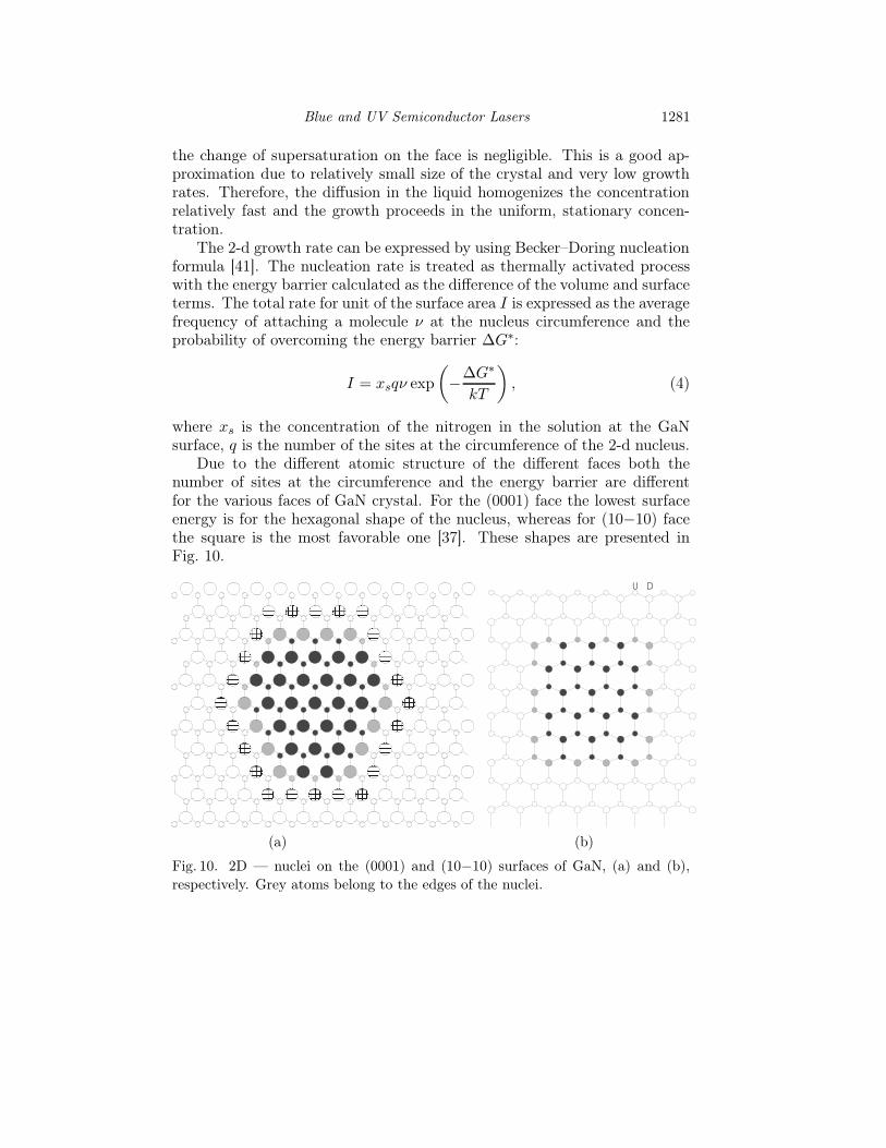
Due to the different atomic structure of the different faces both thenumber of sites at the circumference and the energy barrier are differentfor the various faces of GaN crystal. For the (0001) face the lowest surfaceenergy is for the hexagonal shape of the nucleus, whereas for (10−10) facethe square is the most favorable one [37]. These shapes are presented inFig. 10.
DU
(a) (b)
Fig. 10. 2D — nuclei on the (0001) and (10−10) surfaces of GaN, (a) and (b),respectively. Grey atoms belong to the edges of the nuclei.
1282 S. Krukowski et al.
Using this formulation the 2-d nucleation rates can be expressed as thedifference between the equilibrium and actual chemical potentials function∆µ which can be expressed in terms of the supersaturation σ and the tem-perature T :
∆µ = RT ln σ = RT ln
(
x − xeq(T )
xeq(T )
)
, (5)
where x and xs(T ) are the nitrogen concentration at the GaN surface andthe equilibrium concentration at the growth temperature (Fig. 3).
For the polar (0001) surface, the nucleation rate is [37]:
I = νxs
(
6φ
∆µ+ 6
)
exp
[
− 1
RT
(
3φ2
∆µ− 3∆µ
4
)]
, (6a)
whereas for the (10−10), the nucleation rate is [37]:
I = νxs
(
4φ
∆µ− 1
)
exp
[
− 1
RT
(
2φ2
∆µ− ∆µ
8
)]
, (6b)
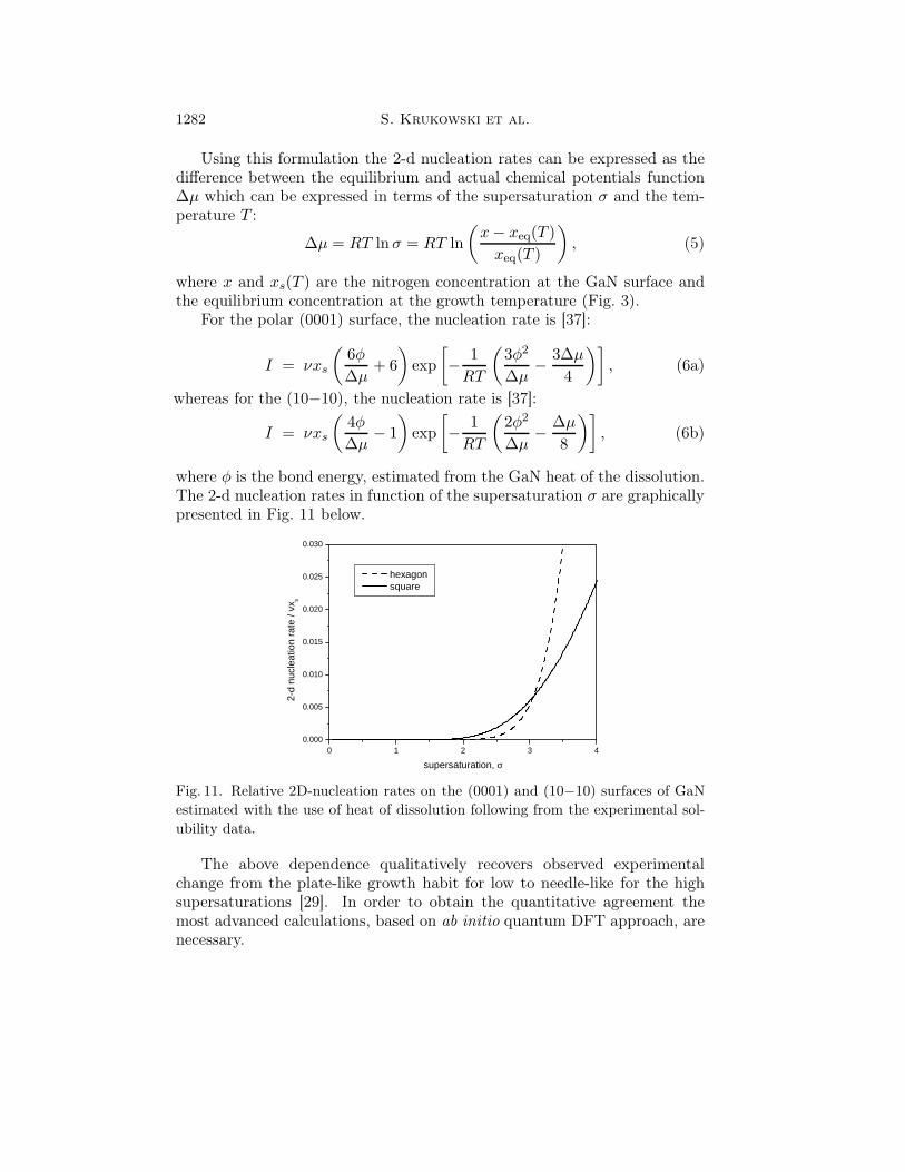
where φ is the bond energy, estimated from the GaN heat of the dissolution.The 2-d nucleation rates in function of the supersaturation σ are graphicallypresented in Fig. 11 below.
0 1 2 3 40.000
0.005
0.010
0.015
0.020
0.025
0.030
2-d
nucl
eatio
n ra
te /
νxs
supersaturation, σ
hexagon square
Fig. 11. Relative 2D-nucleation rates on the (0001) and (10−10) surfaces of GaNestimated with the use of heat of dissolution following from the experimental sol-ubility data.
The above dependence qualitatively recovers observed experimentalchange from the plate-like growth habit for low to needle-like for the highsupersaturations [29]. In order to obtain the quantitative agreement themost advanced calculations, based on ab initio quantum DFT approach, arenecessary.
Blue and UV Semiconductor Lasers 1283
2.5. Physical properties of GaN grown by HNPS method2.5.1. Point defects
As it was already mentioned, the N2 molecules dissociate at the contactwith the Ga surface. However, to approach the surface they have to overcomequite high (about 3.5 eV) potential barrier which lowers substantially therate of nitrogen dissociation and its further dissolution in the metal. Foroxygen interacting with Ga, there is no potential barrier for dissociation [42]and therefore even traces of this impurity in the growth system are sourceof the unintentional oxygen doping of GaN. Consequently the crystals arestrongly n-type with free electron concentration of about 5 × 1019 cm−3
(metallic conductivity) and mobility of about 60 cm2/Vs [43]. These freecarriers can be fully eliminated by a Mg acceptor added into the growthsolution. Then the resistivity of the crystals becomes as high as 104–106 Ωcmat 300 K. Usually the GaN:Mg crystals become p-type with the activationenergy of 200 meV, at temperatures slightly exceeding 300 K. More detailedanalysis of the electrical properties of pressure grown Mg doped GaN crystalscan be found in Ref. [44].
The presence of the native point defects in the crystals has been checkedby positron annihilation measurements [45]. High concentration of Ga va-cancies VGa has been found in the conductive crystals in contrast to theMg-doped samples where no Ga-vacancies have been observed. This agreedwith theoretical prediction that the formation energy of VGa decreases withthe increase in the Fermi level energy [46,47] suggesting that in the creationof these defects thermodynamics plays a role. The difference in the PL spec-tra [48] of the conductive (strong yellow emission) and Mg-doped crystals(no yellow emission, blue Mg-related signal) supported the view that VGa isinvolved in yellow luminescence in GaN.
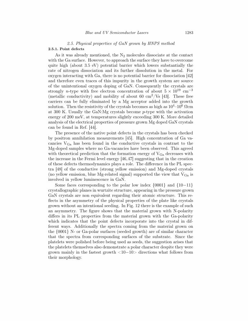
Some faces corresponding to the polar low index 0001 and 10−11crystallographic planes in wurtzite structure, appearing in the pressure grownGaN crystals are non equivalent regarding their atomic structure. This re-flects in the asymmetry of the physical properties of the plate like crystalsgrown without an intentional seeding. In Fig. 12 there is the example of suchan asymmetry. The figure shows that the material grown with N-polaritydiffers in its PL properties from the material grown with the Ga-polaritywhich indicates that the point defects incorporate into the crystal in dif-ferent ways. Additionally the spectra coming from the material grown onthe 0001 N- or Ga-polar surfaces (seeded growth) are of similar characterthat the spectra from corresponding surfaces of the substrate. Since theplatelets were polished before being used as seeds, the suggestion arises thatthe platelets themselves also demonstrate a polar character despite they weregrown mainly in the fastest growth <10−10> directions what follows fromtheir morphology.
1284 S. Krukowski et al.
2.5 3.0 3.5 0
2000
4000
6000
seeded growth
substrate
T=10K 3mW HeCd
Inte
nsity
[arb
.uni
ts.]
Energy [eV]
GaN
2.5 3.0 3.5 0
1000
2000
3000
4000
seeded growth
substrate
Inte
nsity
[arb
.uni
ts.]
Energy [eV]
Fig. 12. Photoluminescence of GaN layers grown on different sides of HP grownGaN substrate and the substrate itself. Center — scheme of the layers and thesubstrate.
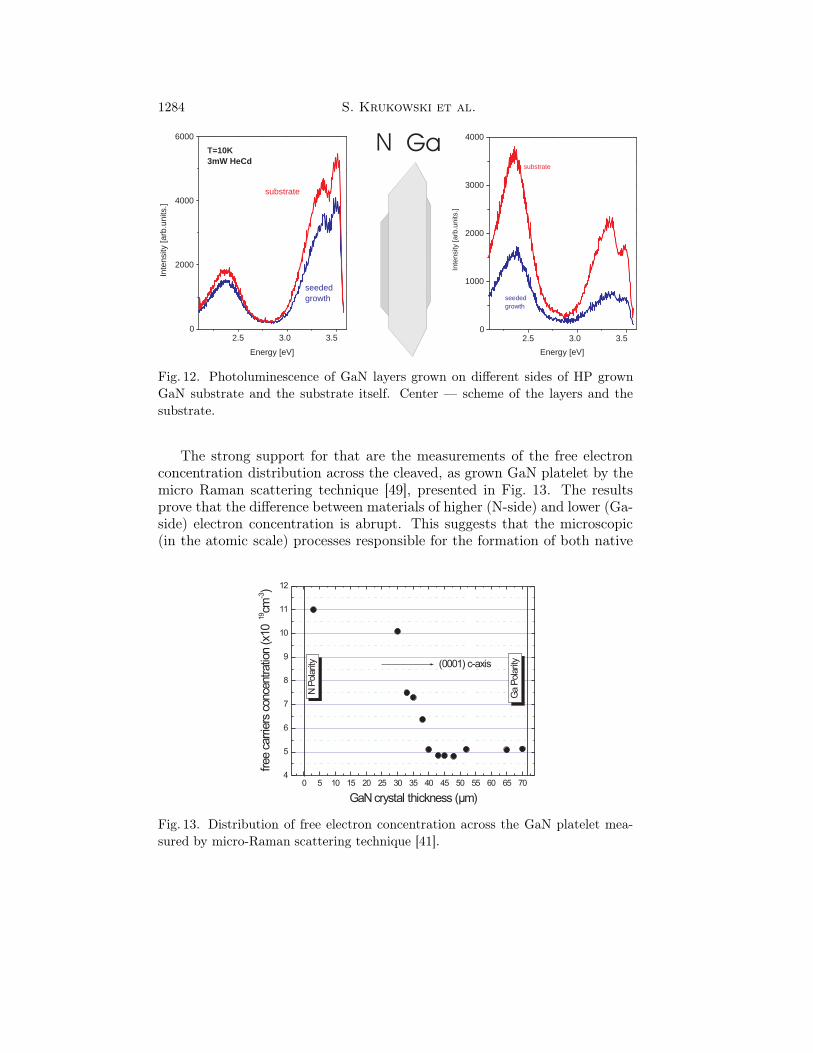
The strong support for that are the measurements of the free electronconcentration distribution across the cleaved, as grown GaN platelet by themicro Raman scattering technique [49], presented in Fig. 13. The resultsprove that the difference between materials of higher (N-side) and lower (Ga-side) electron concentration is abrupt. This suggests that the microscopic(in the atomic scale) processes responsible for the formation of both native
0 5 10 15 20 25 30 35 40 45 50 55 60 65 704
5
6
7
8
9
10
11
12
Frayssinet et al. - Fig. 03 -
(0001) c-axis
NP
ola
rity
Ga
Pola
rity
free
carr
iers
conce
ntratio
n(x
10
19cm
-3)
GaNcrystal thickness (µm)
Fig. 13. Distribution of free electron concentration across the GaN platelet mea-sured by micro-Raman scattering technique [41].
Blue and UV Semiconductor Lasers 1285
and impurity related point defects are related to the kinetic factors relatedto the growth on different faces of GaN. It also indicates that the diffusionof the donors which are the sources of the free electrons, is negligible at thegrowth temperature.
Such approach allows to understand yet another result of positron anni-hilation measurements [50], showing that the concentration of Ga vacanciesis much higher at the Ga-side than at the N-side of the n-type GaN platelets.It seems surprising at the first sight, since on the Ga-polar (0001) surface,the surface Ga atoms are bonded to the surface by three bonds whereasto the opposite one only by a one bond. If we assume, however, that theincorporation of the Ga atoms occurs on the 10−11 polar surfaces, thepositron annihilation results become more consistent since on the (10−11)face adjacent to the (0001) one, the Ga atoms can be bonded by one ortwo bonds whereas on the opposite (−101−1) polar surface adjacent to the(000−1) one, the Ga surface atoms are bonded by two or three bonds.
2.5.2. Extended defects
The structure of the pressure grown GaN crystals has been investigatedusing various techniques, including X-ray diffraction (XRD) [51], transmis-sion electron microscopy (TEM) i.e. [38, 52–54], defect selective etching(DSE) [55] and atomic force microscopy (AFM) of the homoepitaxial lay-ers [56].
In case of the conductive crystals, the shape of the X-ray rocking curves((0002)CuKα reflection) depends on the size of the crystal. The full widthsat half maximum (FWHM) are 20–30 arcsec for 1mm crystals and 30–40 arc-sec for 1–3 mm ones. For larger platelets the rocking curves often split intoa few ∼ 30–40 arcsec peaks showing a presence of low angle (1–3 arcmin)boundaries separating grains of a few mm in size. Misorientation betweengrains increases monotonically from end to end of the crystal [51]. It hasbeen suggested that this can be also related to the polar character of theplatelets growth leading to some strain and its subsequent relaxation throughthe formation of the low angle boundaries.
TEM examination by Liliental-Weber et al. [38] showed that the N-polar(000−1) surface of the n-type pressure grown GaN crystals (especially forthe smaller ones) is frequently atomically flat (2–3 single atomic layer stepson the surface) and that the crystals under this surface are practically free ofextended defects. Below the opposite, rough surface, a number of extendeddefects such as stacking faults, dislocation loops and Ga microprecipitatescan be found. The relative thickness of this part usually consists of 10%of the entire thickness of the platelet. It seems that the presence of thesedefects is related to the growth instabilities often observed on the Ga-polarsurface of the crystals grown without an intentional doping.
1286 S. Krukowski et al.
For the use of the crystals as substrates for epitaxy, the near surfacepart of the material being often the result of the unstable growth has tobe removed by polishing and subsequent Reactive Ion Etching (Ga-side) ormechano-chemical polishing (N-side). As a rule the extended defects arenot observed by TEM in the crystals used as substrates for both N and Gapolarity epitaxial growth. Therefore, if the epitaxy is properly performed,both the substrate and the layer quantum structure are free from dislocationsthat can be observed by TEM.
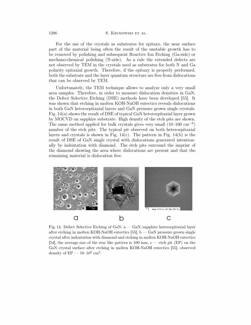
Unfortunately, the TEM technique allows to analyze only a very smallarea samples. Therefore, in order to measure dislocation densities in GaN,the Defect Selective Etching (DSE) methods have been developed [55]. Itwas shown that etching in molten KOH-NaOH eutectics reveals dislocationsin both GaN heteroepitaxial layers and GaN pressure grown single crystals.Fig. 14(a) shows the result of DSE of typical GaN heteroepitaxial layer grownby MOCVD on sapphire substrate. High density of the etch pits are shown.The same method applied for bulk crystals gives very small (10–100 cm−2)number of the etch pits. The typical pit observed on both heteroepitaxiallayers and crystals is shown in Fig. 14(c). The pattern in Fig. 14(b) is theresult of DSE of GaN single crystal with dislocations generated intention-ally by indentation with diamond. The etch pits surround the imprint ofthe diamond showing the area where dislocations are present and that theremaining material is dislocation free.
a b cFig. 14. Defect Selective Etching of GaN: a — GaN/sapphire heteroepitaxial layerafter etching in molten KOH-NaOH eutectics [55], b — GaN pressure grown singlecrystal after indentation with diamond and etching in molten KOH-NaOH eutectics[54], the average size of the star like pattern is 100 mm, c — etch pit (EP) on theGaN crystal surface after etching in molten KOH-NaOH eutectics [55], observeddensity of EP — 10–102 cm2.
Blue and UV Semiconductor Lasers 1287
3. Epitaxy and devices
3.1. Introduction
The spectacular development of GaN-based optoelectronic devices waspossible due to elaboration of the two-step Metal Organic Vapor Phase Epi-taxy (MOVPE) process for the growth of (GaAlIn)N epitaxial structureson highly mismatched sapphire substrates. In these structures dislocationdensities are as high as 108–1010 cm−2 but, nevertheless, very efficient lumi-nescence is possible if the structures contain InGaN [1].
Nakamura suggested that this is due to strong localization of carriers indeep potential wells caused by compositional fluctuation in InGaN alloys [1],which localized the carrier far away from the dislocations and hampered theirrole as nonradiative recombination centers. However, for high injection cur-rents (i.e. in high power LDs), the potential minima are too shallow tocontain all the injected carriers and therefore for lasers, the reduction of dis-location density in the material is much more important than for LEDs. TheNakamura’s model explains in a consistent way the following characteristicsof Nichia optoelectronic devices (both LEDs and LDs) :
• The nitride LEDs containing In in their active structures are muchmore efficient than LEDs with pure GaN active layers (not alloyedwith In).
• InGaN LEDs efficiency does not depend critically on dislocation den-sity (if Al2O3 or ELOG are used) in contrast to the efficiency of In-freeUV diodes.
• At high injection currents, the high dislocation density lowers the ef-ficiency even for InGaN LEDs.
Therefore, one can expect that the elimination of dislocations from thestructures should lead to:
• High efficiency In-free UV LEDs.
• Higher efficiency and higher power of both UV and visible laser diodesthan it is possible with dislocated structures.
• Reduction of the dislocation-related strain in the LD structures.
• Possibility of the reduction of the growth temperature.
• Investigation of p-doping by the use of higher content of Mg.
1288 S. Krukowski et al.
In the following both In-free and In-containing structures are consideredand the results supporting the above expectations are presented.
Crystal growth of dislocation-free nitride structures requires surfacepreparation. Due to the different chemical properties of the Ga-side andthe N-side surfaces, the different surface preparation techniques were devel-oped.
The initial step of the preparation of both sides of GaN plate-like crystalrelies on mechanical polishing of the crystal. The polishing has to removethe surface layer of the GaN crystal which usually contains higher amount ofoxygen and frequently has additional impurities. This layer is grown duringthe last stage of HP growth, i.e. during cooling down of Ga solution underhigh nitrogen pressure. In addition, this procedure served to obtain thestandard and uniform thickness of the substrate, which is very importantfor the processing of the laser structures. Also it is possible to obtain thedesigned misorientation of the substrate in order to assure the best growthof the epitaxial layers.
Since the N-side of GaN surface is chemically active, the subsequentstage of GaN surface preparation is by mechano-chemical polishing. It hasbeen showed that simple chemical etching of the N-side of GaN crystals inKOH 1:5 (1 weight part of KOH is dissolved in 5 weight parts of water) ledto creation of hill and valley structure [55]. The etching slows down after5–7 minutes and is virtually negligible after 20 minutes. After 5 minutesthe skeleton of pyramidal structure is emerging. After 50 minutes of etchinga full pyramidal structure was developed. It is likely that the protectivechemically inert, insoluble oxide layer is created and the etching process isstopped. From the AFM image of this structure it was deduced that theetching ends when the [10−12] faces of the opposite polarity are totallyexposed.
By simultaneous mechanical polishing and chemical etching the chemicalprocess is greatly enhanced. As shown by AFM measurements, the processcan be continued until the creation of perfectly flat surface [57]. The RBSmeasurements showed that the subsurface layer is free of the defects intro-duced during mechanical polishing stage [57, 58].
In contrast to the N-side, the Ga-side of GaN plate-like crystals is muchmore chemically inert. This is particularly unfortunate because only thegrowth on the Ga-side allows to obtain optically active structures necessaryto effective optoelectronic devices (LEDs and LDs). The growth on theN-side has not led to creation of effective LEDs or LDs. The advantageof Ga-terminated (0001) face stems from more effective incorporation ofacceptors than N-terminated (000−1) face. On contrary, N-terminated faceeasier incorporates donors, also impurities, like oxygen [59]. Preparation ofthe Ga-side can be made using more aggressive etching agent which requires
Blue and UV Semiconductor Lasers 1289
protection of more active N-side that is technically difficult. Alternativeway is to use reactive ion etching (RIE) to remove the mechanically damagesubsurface layer. This technique has been developed [60], in which GaN isetched using Cl ions. The chlorine ions bombardment results in formationof volatile Ga-Cl species. It this way the damaged layer is removed, butthe surface morphology is still far from being the flat surface, necessary forhigh quality epitaxial growth. Then by annealing in ammonia and hydrogenmixture this surface structure is removed and the surface is suitable forepitaxy. Typically these annealing processes are performed in the apparatusused in MOVPE.
3.2. Metalorganic chemical vapor epitaxy (MOVPE) on GaN substrates
Metalorganic chemical vapor epitaxy is the most widely used techniquefor growing III-N nitride layers. The MOVPE results reported here wereobtained in IHPP using vertical flow reactor. The gases (N2, H2 and NH3)are purified to ppb level by SAES getter purifiers. The following metal-organic compounds are used: TMG, TMA, TMI as source of group III metalfor growing (Al,Ga,In)N layers, Cp2Mg for Mg-doping, SiH4 for Si-doping.The substrate is heated by an inductive coil that enforces current flow in agraphite (SiC-coated) susceptor.
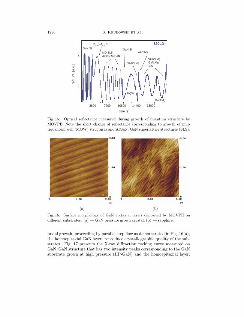
The growth is monitored by laser reflectometry. A typical time varia-tion of the reflected light intensity, obtained during the growth of InGaNbased laser-structure, is presented in Fig. 15. Each oscillation correspondsto change of the thickness of about 1300 Å. The diagram shows that duringa very complicated growth (more than 100 different layers) the amplitudeof oscillation remains almost constant for the same chemical composition,which indicates that the surface roughness was not increased. Using laserreflectometry, it is possible to monitor the growth with 2–3 Å accuracy,what is necessary for the precise determination of the width of the multiplequantum wells (MQW) structure.
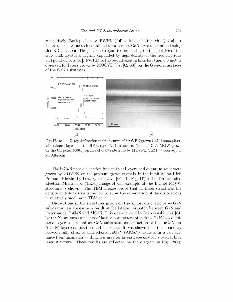
If the surface preparation and the conditions of the epitaxial growth allowgrowth by undisturbed step flow mode, the structure of GaN homoepitaxiallayers, in terms of dislocation density, follows the structure of the GaNsubstrates. Fig. 16 shows the AFM results demonstrating the difference inthe surface morphology of GaN epitaxial layers deposited by MOVPE in thesame run, on GaN crystal and on GaN/sapphire substrate.
The atomic step flow on the surface of the homoepitaxial (GaN/GaN)layer is not perturbed in contrast to the noisy pattern measures after depo-sition of GaN layer on GaN/sapphire substrate containing high density ofthreading dislocations. The dislocations disturb the atomic step flow leadingto entangled step structure shown in Fig. 16(b). In case of high quality epi-
1290 S. Krukowski et al.
3600 7200 10800 14400 18000
3
6
GaN:Mg
AlGaN:Mg /GaN:Mg SLS
GaN:Mg
AlGaN:Mg
MQW
GaN:Si MD-SLS AlGaN:Si/GaN
In 0.09
Ga 0.91
N
GaN:Si
320LD
refl.
int.
[a.u
.]
time [s]
Fig. 15. Optical reflectance measured during growth of quantum structure byMOVPE. Note the short change of reflectance corresponding to growth of mul-tiquantum well (MQW) structures and AlGaN/GaN superlattice structures (SLS).
(a) (b)
Fig. 16. Surface morphology of GaN epitaxial layers deposited by MOVPE ondifferent substrates: (a) — GaN pressure grown crystal, (b) — sapphire.
taxial growth, proceeding by parallel step flow as demonstrated in Fig. 16(a),the homoepitaxial GaN layers reproduce crystallographic quality of the sub-strates. Fig. 17 presents the X-ray diffraction rocking curve measured onGaN/GaN structure that has two intensity peaks corresponding to the GaNsubstrate grown at high pressure (HP-GaN) and the homoepitaxial layer,
Blue and UV Semiconductor Lasers 1291
respectively. Both peaks have FWHM (full widths at half maxima) of about20 arcsec, the value to be obtained for a perfect GaN crystal examined usingthis XRD system. The peaks are separated indicating that the lattice of theGaN bulk crystal is slightly expanded by high density of the free electronsand point defects [61]. FWHM of the bound exciton lines less than 0.5 meV isobserved for layers grown by MOCVD (i.e. [62,63]) on the Ga-polar surfacesof the GaN substrates.
36.36 36.40 36.44 36.48 36.52
0
20000
40000
60000
80000
FWHM=21 arc secFWHM=19 arc sec
GaN layerlow free-electronconcentration
GaN substratehigh free-electronconcentration
inte
nsity
(cp
s)
theta (deg)
(a) (b)
Fig. 17. (a) — X-ray diffraction rocking curve of MOVPE grown GaN homoepitax-ial undoped layer and the HP n-type GaN substrate. (b) — InGaN MQW grownon the Ga-polar (0001) surface of GaN substrate by MOVPE, TEM — courtesy ofM. Albrecht.
The InGaN near dislocation free epitaxial layers and quantum wells weregrown by MOVPE, on the pressure grown crystals, in the Institute for HighPressure Physics by Leszczynski et al. [60]. In Fig. 17(b) the TransmissionElectron Microscopy (TEM) image of one example of the InGaN MQWsstructure is shown. The TEM images prove that in these structures thedensity of dislocations is too low to allow the observation of the dislocationsin relatively small area TEM scan.
Dislocations in the structures grown on the almost dislocation-free GaNsubstrates can appear as a result of the lattice mismatch between GaN andits ternaries: InGaN and AlGaN. This was analyzed by Leszczynski et al. [64]by the X-ray measurements of lattice parameters of various GaN-based epi-taxial layers deposited on GaN substrates as a function of the InGaN (orAlGaN) layer composition and thickness. It was shown that the boundarybetween fully strained and relaxed InGaN (AlGaN) layers is in a safe dis-tance from mismatch — thickness area for layers necessary for a typical bluelaser structure. These results are collected on the diagram in Fig. 18(a).

1292 S. Krukowski et al.
Fig. 18(b) shows an example of the multilayer structure similar to the fullstructure of blue laser. The example confirms that no mismatch dislocationsare generated if the structure is grown on dislocation free GaN substrate.
0.1 1100
1000
10000
boundarybetweenrelaxedandstrainedlayers
strained
relaxed
strain-thicknessinatypicalbluelaser
laye
rth
ickn
ess(A
)
mismatch(%)
(a) (b)
Fig. 18. Critical conditions for III-N ternaries: (a) — X-ray data: open circles —AlGaN relaxed, open squares — AlGaN strained, filled squares — InGaN strained,open squares — InGaN relaxed, (b) — TEM image of the multilayer structuredeposited on GaN substrate by MOCVD, the sequence of layers from the lowerleft corner: n-GaN, n-Al0.11Ga0.89N/n-GaN superlattice, n-GaN, In0.09Ga0.91N,p-GaN, p-Al0.14Ga0.86N/p-GaN superlattice, p-GaN.
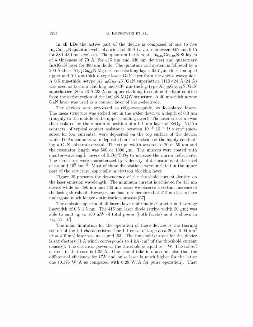
TEM and AFM techniques can probe only an area of a few square mi-crons. Using XRD we examined an area of a few millimeters squared. Fig. 19presents an experimental scan for a laser structure compared with a theo-retical simulation using a dynamical X-ray diffraction theory.
For GaN and AlGaN layers (on the right-hand side of the scan), the peaksare very narrow, not broadened by compositional fluctuations. For InGaN,as expected, the peaks are slightly broader than for a perfect structure.
Even when dislocation-free GaN substrates are used, the LD structurecontains highly lattice-mismatched parts of AlGaN and InGaN that can berelaxed by dislocations. It follows from the defect selective etching thatthe rate of etching is different for layers of various chemical compositionwhich allows to determine where the dislocations originate. This knowledgeis crucial and serves as convenient tool in optimizing the deposition of theLD structure.
The etching experiments were performed in the modified molten basessystem [65] in the temperature 450C, for 40 minutes in order to deter-mine the layer of the laser structure where the dislocations emerge. Theetched samples were examined by the scanning electron microscopy (SEM),
Blue and UV Semiconductor Lasers 1293
-20000 -15000 -10000 -5000 0 5000 10000 15000 0.01
0.1
1
10
100
1000
10000
100000
1000000
experiment simulation
inte
nsity
[a. u
.]
2theta [rel. sec.]
Fig. 19. X-ray scan of laser structure. For comparison an X-ray intensity of simu-lated perfect structure is presented.
transmission electron microscopy (TEM) and optical microscopy with dif-ferential interference contrast (DIC). The morphology of the etch pits wasdetermined by the AFM method. 3D etch pits maps and cross sections wereobtained. The results of these measurements indicate that the two classesof the dislocation were discovered [65]. The first class consists of the dislo-cations generated in the p-type GaN below the upper cladding. The secondclass are the dislocations which started at the InGaN MQW. In order toconfirm the dependencies between the structure of the laser and the etch pitshape, the TEM investigations were performed. The results of these TEMmeasurements confirmed the classification based on AFM results.
The differences in the etch pit shapes allow fast determination of theplace where the dislocations were generated. Hence for the large area inves-tigations the AFM study is not necessary. The approximate measurementsof the pits depths may be based on the SEM images. Presented in Ref. [65] isthe example of the area of 6×104 µm2, where only 8 etch pits of the first classwere discovered. There were also 35 pits of the second class giving 63 pits intotal. The pits distribution on this sample surface seems to be homogenous,so these results can be used for the estimation of the etch pits densities forthe whole sample. The total etch pits density was 1.05 × 105 cm−2. Thedensities of the pits associated to the dislocations starting above the MQW,in the MQW and below the MQW were estimated to be 1.3× 10⁴, 5.8× 10⁴
and 3.3 × 104 cm−2, respectively.
1294 S. Krukowski et al.
In all LDs the active part of the device is composed of one to fiveInxGa1−xN quantum wells of a width of 40 Å (x varies between 0.02 and 0.15for 380–430 nm devices). The quantum barriers are In0.02Ga0.98N:Si layersof a thickness of 70 Å (for 415 nm and 430 nm devices) and quaternaryInAlGaN layer for 380 nm diode. The quantum well system is followed by a200 Å-thick Al0.2Ga0.8N:Mg electron blocking layer, 0.07 µm-thick undopedupper and 0.1 µm-thick n-type lower GaN layer form the device waveguide.A 0.5 mm-thick n-type Al0.16Ga0.84N/GaN superlattice (110×24 Å/24 Å)was used as bottom cladding and 0.37 µm-thick p-type Al0.15Ga0.85N/GaNsuperlattice (80×23 Å/23 Å) as upper cladding to confine the light emittedfrom the active region of the InGaN MQW structure. A 40 nm-thick p-typeGaN layer was used as a contact layer of the p-electrode.
The devices were processed as ridge-waveguide, oxide-isolated lasers.The mesa structure was etched out in the wafer down to a depth of 0.3 µm(roughly to the middle of the upper cladding layer). The laser structure wasthen isolated by the e-beam deposition of a 0.1 µm layer of ZrO2. Ni/Aucontacts, of typical contact resistance between 10−3–10−4 Ω × cm2 (mea-sured for low currents), were deposited on the top surface of the device,while Ti/Au contacts were deposited on the backside of the highly conduct-ing n-GaN substrate crystal. The stripe width was set to 20 or 50 µm andthe resonator length was 500 or 1000 µm. The mirrors were coated withquarter-wavelength layers of SiO2/TiO2 to increase the mirror reflectivity.The structures were characterized by a density of dislocations at the levelof around 105 cm−2. Most of these dislocations were initiated in the upperpart of the structure, especially in electron blocking layer.
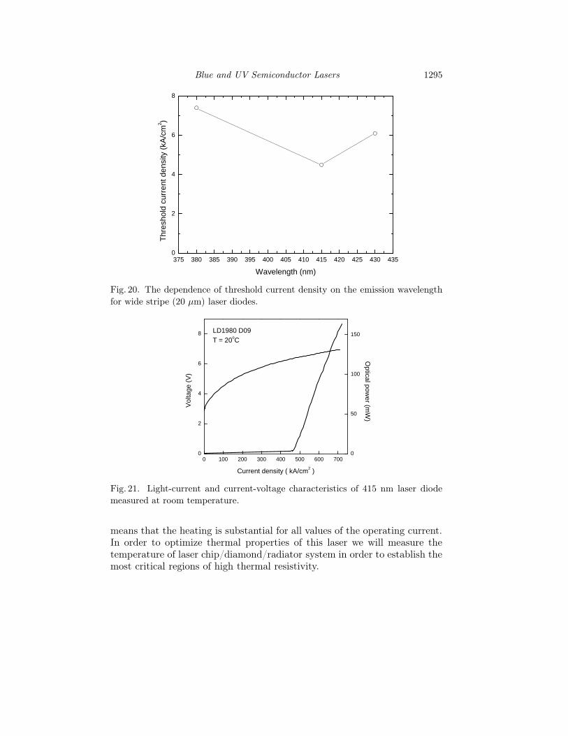
Figure 20 presents the dependence of the threshold current density onthe laser emission wavelength. The minimum current is achieved for 415 nmdevice while for 380 nm and 430 nm lasers we observe a certain increase ofthe lasing threshold. However, one has to remember that 415 nm lasers haveundergone much longer optimization process [67].
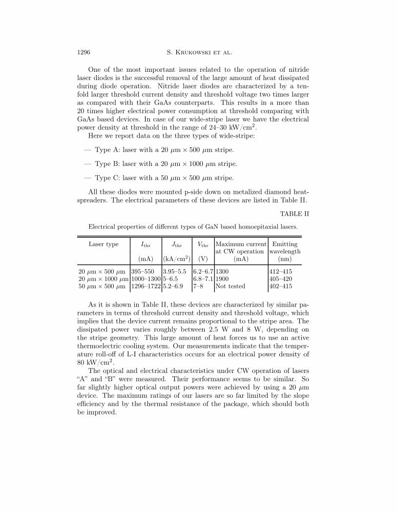
The emission spectra of all lasers have multimode character and averagelinewidth of 0.5–1.5 nm. The 415 nm laser diode (stripe width 20 µm) wasable to emit up to 180 mW of total power (both facets) as it is shown inFig. 21 [67].
The main limitation for the operation of these devices is the thermalroll-off of the L-I characteristic. The L-I curve of large area 20 × 1000 µm2
(λ = 415 nm) laser was measured [63]. The threshold current for this deviceis satisfactory (1 A which corresponds to 4 kA/cm2 of the threshold currentdensity). The electrical power at the threshold is equal to 7 W. The roll-offcurrent in that case is 1.35 A . One should take into account also that thedifferential efficiency for CW and pulse laser is much higher for the latterone (0.176 W/A as compared with 0.28 W/A for pulse operation). That
Blue and UV Semiconductor Lasers 1295
375 380 385 390 395 400 405 410 415 420 425 430 4350
2
4
6
8
Thr
esho
ld c
urre
nt d
ensi
ty (
kA/c
m2 )
Wavelength (nm)
Fig. 20. The dependence of threshold current density on the emission wavelengthfor wide stripe (20 µm) laser diodes.
0 100 200 300 400 500 600 7000
50
100
150
0
2
4
6
8
LD1980 D09T = 20oC
Current density ( kA/cm2 )
Optical pow
er (mW
)
Vol
tage
(V
)
Fig. 21. Light-current and current-voltage characteristics of 415 nm laser diodemeasured at room temperature.
means that the heating is substantial for all values of the operating current.In order to optimize thermal properties of this laser we will measure thetemperature of laser chip/diamond/radiator system in order to establish themost critical regions of high thermal resistivity.
1296 S. Krukowski et al.
One of the most important issues related to the operation of nitridelaser diodes is the successful removal of the large amount of heat dissipatedduring diode operation. Nitride laser diodes are characterized by a ten-fold larger threshold current density and threshold voltage two times largeras compared with their GaAs counterparts. This results in a more than20 times higher electrical power consumption at threshold comparing withGaAs based devices. In case of our wide-stripe laser we have the electricalpower density at threshold in the range of 24–30 kW/cm2.
Here we report data on the three types of wide-stripe:
— Type A: laser with a 20 µm × 500 µm stripe.
— Type B: laser with a 20 µm × 1000 µm stripe.
— Type C: laser with a 50 µm × 500 µm stripe.
All these diodes were mounted p-side down on metalized diamond heat-spreaders. The electrical parameters of these devices are listed in Table II.
TABLE II
Electrical properties of different types of GaN based homoepitaxial lasers.
Laser type Ithr Jthr Vthr Maximum current Emittingat CW operation wavelength
(mA) (kA/cm2) (V) (mA) (nm)
20 µm × 500 µm 395–550 3.95–5.5 6.2–6.7 1300 412–41520 µm × 1000 µm 1000–1300 5–6.5 6.8–7.1 1900 405–42050 µm × 500 µm 1296–1722 5.2–6.9 7–8 Not tested 402–415
As it is shown in Table II, these devices are characterized by similar pa-rameters in terms of threshold current density and threshold voltage, whichimplies that the device current remains proportional to the stripe area. Thedissipated power varies roughly between 2.5 W and 8 W, depending onthe stripe geometry. This large amount of heat forces us to use an activethermoelectric cooling system. Our measurements indicate that the temper-ature roll-off of L-I characteristics occurs for an electrical power density of80 kW/cm2.
The optical and electrical characteristics under CW operation of lasers“A” and “B” were measured. Their performance seems to be similar. Sofar slightly higher optical output powers were achieved by using a 20 µmdevice. The maximum ratings of our lasers are so far limited by the slopeefficiency and by the thermal resistance of the package, which should bothbe improved.
Blue and UV Semiconductor Lasers 1297
So far, laser “C” was not successfully tested under CW operation becauseof thermal management problems. However, we believe that, with an im-proved mounting scheme, this type of laser may provide a good solution forthe 1 W emission range.
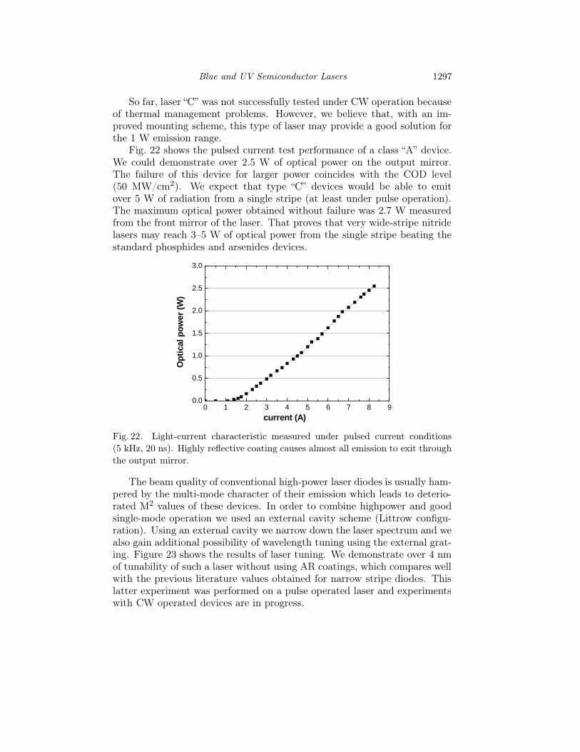
Fig. 22 shows the pulsed current test performance of a class “A” device.We could demonstrate over 2.5 W of optical power on the output mirror.The failure of this device for larger power coincides with the COD level(50 MW/cm2). We expect that type “C” devices would be able to emitover 5 W of radiation from a single stripe (at least under pulse operation).The maximum optical power obtained without failure was 2.7 W measuredfrom the front mirror of the laser. That proves that very wide-stripe nitridelasers may reach 3–5 W of optical power from the single stripe beating thestandard phosphides and arsenides devices.
0 1 2 3 4 5 6 7 8 90.0
0.5
1.0
1.5
2.0
2.5
3.0
Opt
ical
pow
er (W
)
current (A)
Fig. 22. Light-current characteristic measured under pulsed current conditions(5 kHz, 20 ns). Highly reflective coating causes almost all emission to exit throughthe output mirror.
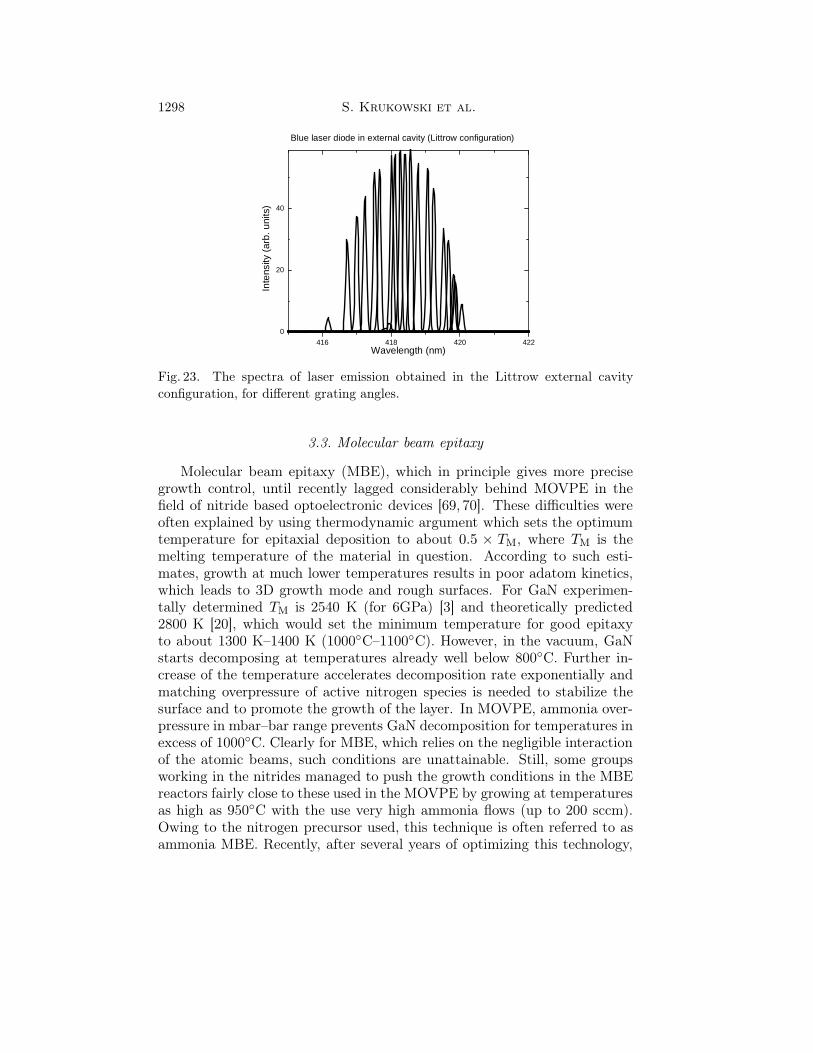
The beam quality of conventional high-power laser diodes is usually ham-pered by the multi-mode character of their emission which leads to deterio-rated M2 values of these devices. In order to combine highpower and goodsingle-mode operation we used an external cavity scheme (Littrow configu-ration). Using an external cavity we narrow down the laser spectrum and wealso gain additional possibility of wavelength tuning using the external grat-ing. Figure 23 shows the results of laser tuning. We demonstrate over 4 nmof tunability of such a laser without using AR coatings, which compares wellwith the previous literature values obtained for narrow stripe diodes. Thislatter experiment was performed on a pulse operated laser and experimentswith CW operated devices are in progress.
1298 S. Krukowski et al.
416 418 420 422
0
20
40
Blue laser diode in external cavity (Littrow configuration)
Inte
nsity
(ar
b. u
nits
)
Wavelength (nm)
Fig. 23. The spectra of laser emission obtained in the Littrow external cavityconfiguration, for different grating angles.
3.3. Molecular beam epitaxy
Molecular beam epitaxy (MBE), which in principle gives more precisegrowth control, until recently lagged considerably behind MOVPE in thefield of nitride based optoelectronic devices [69, 70]. These difficulties wereoften explained by using thermodynamic argument which sets the optimumtemperature for epitaxial deposition to about 0.5 × TM, where TM is themelting temperature of the material in question. According to such esti-mates, growth at much lower temperatures results in poor adatom kinetics,which leads to 3D growth mode and rough surfaces. For GaN experimen-tally determined TM is 2540 K (for 6GPa) [3] and theoretically predicted2800 K [20], which would set the minimum temperature for good epitaxyto about 1300 K–1400 K (1000C–1100C). However, in the vacuum, GaNstarts decomposing at temperatures already well below 800C. Further in-crease of the temperature accelerates decomposition rate exponentially andmatching overpressure of active nitrogen species is needed to stabilize thesurface and to promote the growth of the layer. In MOVPE, ammonia over-pressure in mbar–bar range prevents GaN decomposition for temperatures inexcess of 1000C. Clearly for MBE, which relies on the negligible interactionof the atomic beams, such conditions are unattainable. Still, some groupsworking in the nitrides managed to push the growth conditions in the MBEreactors fairly close to these used in the MOVPE by growing at temperaturesas high as 950C with the use very high ammonia flows (up to 200 sccm).Owing to the nitrogen precursor used, this technique is often referred to asammonia MBE. Recently, after several years of optimizing this technology,
Blue and UV Semiconductor Lasers 1299
Hooper et al. [71] from Sharp Laboratories of Europe demonstrated the firstMBE grown “violet” LDs, operating at room temperature under pulsed con-ditions. In spite of its potential advantages for both optoelectronic [71] andelectronic [72] devices, ammonia MBE has not been the technique of choicefor the majority of nitride MBE community. Indeed, the corrosive natureof ammonia compounded by its large flows creates additional hazards andtechnological challenges as well as leads to often undesirable high hydro-gen background during the epitaxial process. In the more widely employedplasma assisted MBE (PA-MBE) [72], purified nitrogen gas is activated us-ing an RF-plasma and supplied to the growing surface at typical flow ratesof 1–2 sccm. The technique already proved its potential for the growth ofhigh quality structures for electronic components [73], but until now onlylimited success was reported in the area of optoelectronic devices [74]. Theturning point for GaN growth with PA-MBE was the discovery that Ga richconditions are necessary for growth of high quality GaN and AlGaN/GaNheterostructures. High quality layers and interfaces were demonstrated attemperature range of 650–750C, much lower than required for the growthof similar structures with ammonia [75–79]. In our earlier works we opti-mized the growth conditions for high quality GaN and AlGaN/GaN hetero-junctions in Ga rich regime, and demonstrated (i) the record high electronmobility of two-dimensional electron gas at the AlGaN/GaN interface and(ii) very narrow photoluminescence lines from GaN epitaxial layers [62,63].Extensive study of the growth of nitride structures with In as the surfactantenabled us to grow first InGaN LDs by PA-MBE [80]. Recent ab initio cal-culations explain that smooth, step-flow growth of GaN (AlGaN, InGaN)achieved at relatively low temperatures is possible because of existence ofa very efficient lateral diffusion channel for adatoms on semiconductor sur-face just below the dynamically created thin (two or one layer) Ga or Infilm [81–83]. Surprisingly small activation energies for this so called adlayerenhanced lateral diffusion (AELD) enable high quality epitaxy at tempera-tures much lower than expected from mentioned earlier estimates based onGaN melting point. In this work, we investigate parameters of LDs withdifferent number of InGaN QWs grown by this new PA-MBE technique.
The LDs structures were grown in custom designed V90 VG Semiconbased MBE system (now Oxford). Ultra-high purity gas handling man-ifold together with Veeco UniBulb RF Plasma cell was used as a sourceof activated nitrogen. The LDs structures were deposited on conductive,very low dislocation density, high-pressure-grown GaN bulk substrates [4].The epi-ready bulk substrates were prepared in the three-step process ofmechano-polishing, dry etching and deposition of 2 µm GaN:Si buffer layerin the MOVPE reactor. The back sides of the substrates were coated with0.7 µm of molybdenum layer to improve the thermal coupling for radiative
1300 S. Krukowski et al.
heating. Special holders capable of accommodating small irregularly shapedsubstrates (5×5 to 10×10 mm approximate size) and designed to minimizeedge effects ensured high temperature uniformity across the entire substratearea. The LDs structures consisted of the following sequence of layers: the200 nm of GaN:Si buffer layer was followed by 0.55 µm Al0.08Ga0.92N:Sicladding layer. The wave guide was asymmetric with lower part consistingof 100 nm GaN:Si and 40 nm In0.01Ga0.99N:Si. Depending on the struc-ture, five, three or two undoped 4 nm thick In0.09Ga0.91N Quantum Wells(QW) with 7 nm In0.01Ga0.99N:Si barriers were deposited in the active re-gion. 14 nm In0.01Al0.16Ga0.83N:Mg blocking layer was followed by 70 nmIn0.01Ga0.99N:Mg upper wave guide. The upper cladding consisted of 80pairs of uniformly Mg doped In0.01Ga0.99N/In0.01Al0.16Ga0.83N short periodsuperlattice (2.5/2.5 nm). The contact layer was 100 nm GaN:Mg or In-GaN:Mg. Doping levels for n-type layers was 5 × 1018 cm−3, while holeconcentration obtained from Hall effect measurements on a reference 0.3 µmthick In0.01Ga0.99N:Mg layer was 2 × 1018 cm−3.
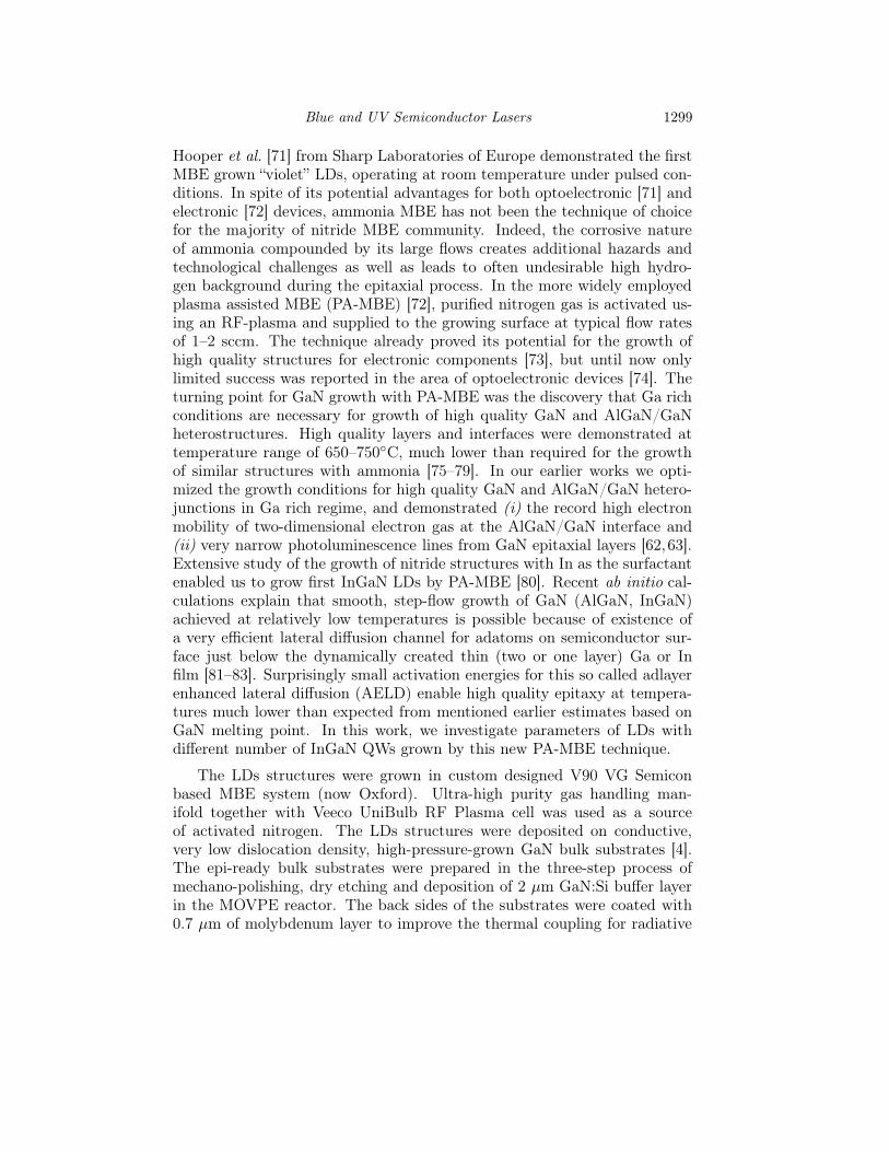
Fig. 24. TEM picture of 3QWs laser diode structure.
The growth temperature for GaN and AlGaN layers was 710C (growthat Ga-rich regime), while QWs and p-type cladding were grown at 590C(growth at In-rich regime). To enable high quality growth, the excess Gaand In fluxes were precisely chosen to form dynamically stable metal filmon semiconductor surface which enhance lateral adatom mobility [78, 81].We used solid sources (high purity Si and Mg) for n and p type doping.No post growth annealing was necessary to activate p-type conductivity. In
Blue and UV Semiconductor Lasers 1301
Fig. 24 we show state of the art of the PA-MBE technology — transmis-sion electron microscope (TEM) picture of laser diode structure containing3 InGaN/InGaN QWs.
The laser diode devices were processed as ridge-waveguide, oxide-isolatedlaser. The mesa structures were etched out in the wafers down to a depthof 0.35 µm. The laser structures were then isolated by e-beam depositionof a 0.2 µm layer of SiOx. The final devices had the stripe width of 15 µmand the resonator length of 500 µm. The oxidized Ni/Au ohmic contactswere deposited on the top surface of the devices, while Ti/Au contacts weredeposited on the backside of the highly conducting n-GaN substrates. Thetested devices had cleaved uncoated mirrors.
The lasers operation was demonstrated at room temperature using 50 nspulses at 0.25% duty cycle. Fig. 25 presents the light-current-voltage(L-I-V) characteristics for typical LDs. A sharp increase of the light powervisible at the current of about 1 A and 9 V bias is indicative of the laseroperation. The lowest threshold current obtained for our lasers was 680 mA(at 8.2 V bias) which gives threshold current density of 9 kA/cm2. Theslope efficiency per facet calculated from L-I plot was 0.35 W/A for 5 QWsand 0.47 W/A for 2 QWs device . The maximum output optical power wasmeasured to be 1.1 W for the LDs with 2 QWs. Strong narrowing of thespectral line was detected above the threshold current (see Fig. 26). Forthis device multimode lasing was observed at 408 nm with mode spacingclose to 0.53 Å, which indicated the presence of longitudinal modes. Thetotal linewidth of emission is close to 0.4 nm. We would like to point outthat threshold currents and voltages for 2 and 5 QWs LDs are very similar.Since other device parameters are not changed, this result might indicatethat only two quantum wells contribute to the lasing operation for the fiveQWs device, pointing towards possible structure design issues. In fact, theparameters of our laser diodes, the output power in particular, are as goodas the early MOVPE LDs or better.
The very important factor responsible for laser diode parameters isp-type doping. Effective p-type doping of GaN is still a subject of inten-sive studies because it is crucial for nitride-based LEDs and LDs. The lowelectrical activation of Mg acceptor in GaN, due to its high ionization energy,requires very high doping level of Mg to obtain desirable hole concentrations.It was already reported that growth of GaN:Mg by PA-MBE resulted in highp-type conductivity without any post growth annealing and with very sharpMg doping profiles [84–86]. Systematic study of the Mg doping of GaN bySmorchkova et al. [84] showed that for the constant growth temperature,Mg flux controls p-type conductivity. The hole concentration as high as1.3× 1018 cm−3 was achieved for Mg doping of 1020 cm−3. As it was shownby Haus et al. [85], growth at low temperatures increases Mg sticking coef-
1302 S. Krukowski et al.
0 1 2 3 40.0
0.2
0.4
0.6
0.8
1.0
1.2
2 QWs 5 Qws
0.35W/A
0.47 W/A
Opt
ical
pow
er in
pul
se (
W)
Current, I (A)
Fig. 25. Light–current characteristics for 2 (solid line) and 5 (dashed line) In-GaN/InGaN QWs laser diodes grown by plasma assisted molecular beam epitaxy.Laser diodes were operated at pulse mode.
400 405 410 415 420
(b)
(a)
x100
T=295K
Pho
ton
coun
t (ar
b. u
nits
)
Wavelength (nm)
Fig. 26. The emission spectra of laser diode operating below (b) and above (a)lasing threshold for 5 InGaN/InGaN QWs laser diodes.
ficient considerably which can be an efficient method to achieve higher Mgdoping level. However, as it was pointed out there, the Mg atoms enterGaN layer for Ga or N rich conditions at the same level, but for N richregime, the Mg acceptors can be compensated by the presence of donors likeGa vacancies mainly due to the low quality of grown layers. For very highMg flux, when the Mg surface coverage is about 1 ML, the polarity inver-sion (PI) from Ga to N on GaN layer can take place [87–89], which leads tothe abrupt decrease of the Mg doping efficiency and deteriorate dramaticallycrystal quality. Therefore, the PI effect is a main limiting factor in achievinghigh Mg content in GaN layers.
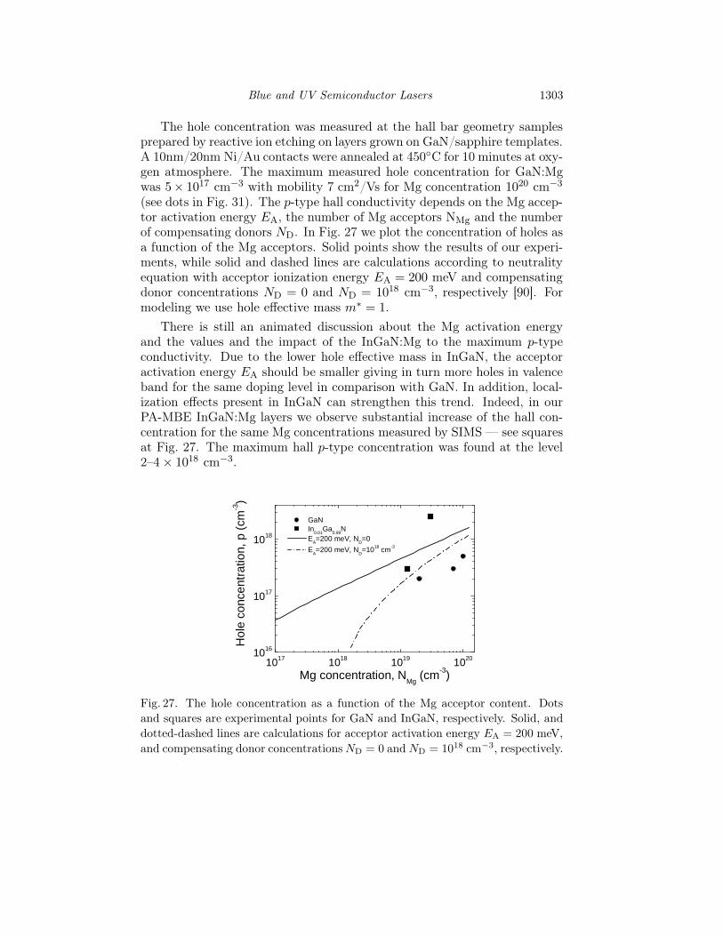
Blue and UV Semiconductor Lasers 1303
The hole concentration was measured at the hall bar geometry samplesprepared by reactive ion etching on layers grown on GaN/sapphire templates.A 10nm/20nm Ni/Au contacts were annealed at 450C for 10 minutes at oxy-gen atmosphere. The maximum measured hole concentration for GaN:Mgwas 5× 1017 cm−3 with mobility 7 cm2/Vs for Mg concentration 1020 cm−3
(see dots in Fig. 31). The p-type hall conductivity depends on the Mg accep-tor activation energy EA, the number of Mg acceptors NMg and the numberof compensating donors ND. In Fig. 27 we plot the concentration of holes asa function of the Mg acceptors. Solid points show the results of our experi-ments, while solid and dashed lines are calculations according to neutralityequation with acceptor ionization energy EA = 200 meV and compensatingdonor concentrations ND = 0 and ND = 1018 cm−3, respectively [90]. Formodeling we use hole effective mass m∗ = 1.
There is still an animated discussion about the Mg activation energyand the values and the impact of the InGaN:Mg to the maximum p-typeconductivity. Due to the lower hole effective mass in InGaN, the acceptoractivation energy EA should be smaller giving in turn more holes in valenceband for the same doping level in comparison with GaN. In addition, local-ization effects present in InGaN can strengthen this trend. Indeed, in ourPA-MBE InGaN:Mg layers we observe substantial increase of the hall con-centration for the same Mg concentrations measured by SIMS — see squaresat Fig. 27. The maximum hall p-type concentration was found at the level2–4 × 1018 cm−3.
1017 1018 1019 10201016
1017
1018
Hol
e co
ncen
trat
ion,
p (
cm-3)
Mg concentration, NMg
(cm-3)
GaN In
0.01Ga
0.99N
EA=200 meV, N
D=0
EA=200 meV, N
D=1018 cm-3
Fig. 27. The hole concentration as a function of the Mg acceptor content. Dotsand squares are experimental points for GaN and InGaN, respectively. Solid, anddotted-dashed lines are calculations for acceptor activation energy EA = 200 meV,and compensating donor concentrations ND = 0 and ND = 1018 cm−3, respectively.
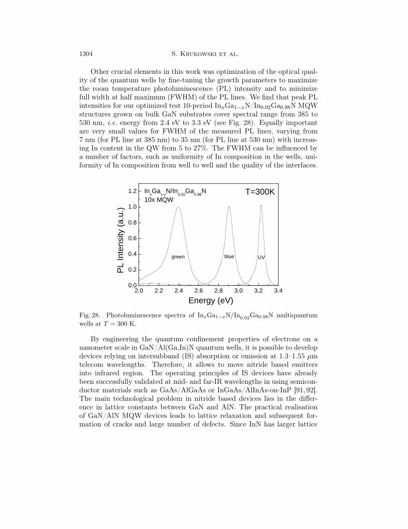
1304 S. Krukowski et al.
Other crucial elements in this work was optimization of the optical qual-ity of the quantum wells by fine-tuning the growth parameters to maximizethe room temperature photoluminescence (PL) intensity and to minimizefull width at half maximum (FWHM) of the PL lines. We find that peak PLintensities for our optimized test 10-period InxGa1−xN/In0.02Ga0.98N MQWstructures grown on bulk GaN substrates cover spectral range from 385 to530 nm, i.e. energy from 2.4 eV to 3.3 eV (see Fig. 28). Equally importantare very small values for FWHM of the measured PL lines, varying from7 nm (for PL line at 385 nm) to 35 nm (for PL line at 530 nm) with increas-ing In content in the QW from 5 to 27%. The FWHM can be influenced bya number of factors, such as uniformity of In composition in the wells, uni-formity of In composition from well to well and the quality of the interfaces.
2.0 2.2 2.4 2.6 2.8 3.0 3.2 3.40.0
0.2
0.4
0.6
0.8
1.0
1.2
UVbluegreen
InxGa
1-xN/In
0.02Ga
0.98N
10x MQWT=300K
PL
Inte
nsity
(a.
u.)
Energy (eV)
Fig. 28. Photoluminescence spectra of InxGa1−xN/In0.02
Ga0.98N multiquantumwells at T = 300 K.
By engineering the quantum confinement properties of electrons on ananometer scale in GaN/Al(Ga,In)N quantum wells, it is possible to developdevices relying on intersubband (IS) absorption or emission at 1.3–1.55 µmtelecom wavelengths. Therefore, it allows to move nitride based emittersinto infrared region. The operating principles of IS devices have alreadybeen successfully validated at mid- and far-IR wavelengths in using semicon-ductor materials such as GaAs/AlGaAs or InGaAs/AlInAs-on-InP [91, 92].The main technological problem in nitride based devices lies in the differ-ence in lattice constants between GaN and AlN. The practical realisationof GaN/AlN MQW devices leads to lattice relaxation and subsequent for-mation of cracks and large number of defects. Since InN has larger lattice
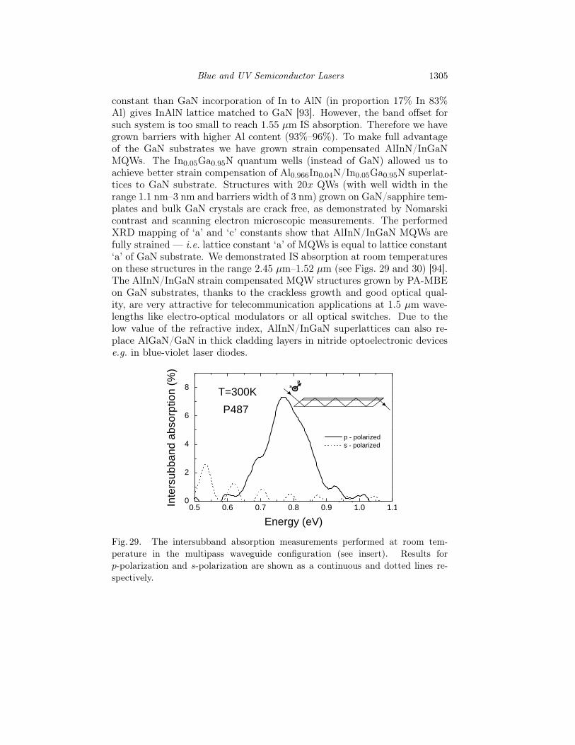
Blue and UV Semiconductor Lasers 1305
constant than GaN incorporation of In to AlN (in proportion 17% In 83%Al) gives InAlN lattice matched to GaN [93]. However, the band offset forsuch system is too small to reach 1.55 µm IS absorption. Therefore we havegrown barriers with higher Al content (93%–96%). To make full advantageof the GaN substrates we have grown strain compensated AlInN/InGaNMQWs. The In0.05Ga0.95N quantum wells (instead of GaN) allowed us toachieve better strain compensation of Al0.966In0.04N/In0.05Ga0.95N superlat-tices to GaN substrate. Structures with 20x QWs (with well width in therange 1.1 nm–3 nm and barriers width of 3 nm) grown on GaN/sapphire tem-plates and bulk GaN crystals are crack free, as demonstrated by Nomarskicontrast and scanning electron microscopic measurements. The performedXRD mapping of ‘a’ and ‘c’ constants show that AlInN/InGaN MQWs arefully strained — i.e. lattice constant ‘a’ of MQWs is equal to lattice constant‘a’ of GaN substrate. We demonstrated IS absorption at room temperatureson these structures in the range 2.45 µm–1.52 µm (see Figs. 29 and 30) [94].The AlInN/InGaN strain compensated MQW structures grown by PA-MBEon GaN substrates, thanks to the crackless growth and good optical qual-ity, are very attractive for telecommunication applications at 1.5 µm wave-lengths like electro-optical modulators or all optical switches. Due to thelow value of the refractive index, AlInN/InGaN superlattices can also re-place AlGaN/GaN in thick cladding layers in nitride optoelectronic devicese.g. in blue-violet laser diodes.
0.5 0.6 0.7 0.8 0.9 1.0 1.10
2
4
6
8 p
s
P487
T=300K
Inte
rsub
band
abs
orpt
ion
(%)
Energy (eV)
p - polarized s - polarized
Fig. 29. The intersubband absorption measurements performed at room tem-perature in the multipass waveguide configuration (see insert). Results forp-polarization and s-polarization are shown as a continuous and dotted lines re-spectively.
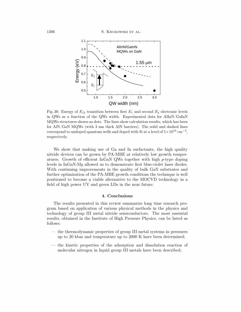
1306 S. Krukowski et al.
1.0 1.5 2.0 2.5 3.0
0.5
0.6
0.7
0.8
0.9
1.0
1.1
E1
E2
AlInN/GaInNMQWs on GaN
1.55 µm
Ene
rgy
(eV
)
QW width (nm)
Fig. 30. Energy of E12 transition between first E1 and second E2 electronic levelsin QWs as a function of the QWs width. Experimental data for AlInN/GaInNMQWs structures shown as dots. The lines show calculation results, which has beenfor AlN/GaN MQWs (with 3 nm thick AlN barriers). The solid and dashed linescorrespond to undoped quantum wells and doped with Si at a level of 5×1019 cm−3,respectively.
We show that making use of Ga and In surfactants, the high qualitynitride devices can be grown by PA-MBE at relatively low growth temper-atures. Growth of efficient InGaN QWs together with high p-type dopinglevels in InGaN:Mg allowed us to demonstrate first blue-violet laser diodes.With continuing improvements in the quality of bulk GaN substrates andfurther optimization of the PA-MBE growth conditions the technique is wellpositioned to become a viable alternative to the MOCVD technology in afield of high power UV and green LDs in the near future.
4. Conclusions
The results presented in this review summarize long time research pro-gram based on application of various physical methods in the physics andtechnology of group III metal nitride semiconductors. The most essentialresults, obtained in the Institute of High Pressure Physics, can be listed asfollows:
— the thermodynamic properties of group III metal systems in pressuresup to 20 kbar and temperature up to 2000 K have been determined;
— the kinetic properties of the adsorption and dissolution reaction ofmolecular nitrogen in liquid group III metals have been described;

Blue and UV Semiconductor Lasers 1307
— crystal growth of substrate quality GaN crystals has been investigated.The research led to the development of the technology of the growthof substrate quality n-type GaN crystals for optoelectronics;
— the two basic epitaxy methods: MOVPE and MBE, were developedand applied for deposition of high quality homoepitaxial layers andquantum well structures;
— the development of dislocation free nitride layers and structures allowsto extend the temperature range used in epitaxy for blue power LDs.This opens the possibility of construction of high power green and UVLDs;
— the development of the QW structures and processing technology al-lowed to obtain blue LDs of the efficiency comparable with the bestheteroepitaxial devices.
The research presented in this paper has been supported by the PolishState Committee for Scientific Research grants 8 T11 G 001 2000 C/5013and 7 T08A 015 18 and in part by European Commission within the: Sup-port for Centers of Excellence No ICA1-CT-2000-70005. We would like toacknowledge the financial support from EU within GaNano project STREP505641-1. The calculations presented here used computing facilities of Inter-disciplinary Centre for Mathematical and Computational Modeling of War-saw University (ICM UW).
REFERENCES
[1] S. Nakamura, G. Fasol, The Blue Laser Diodes, Springer Verlag, Berlin 1997.
[2] J.V. Lirman, H.S. Zhdanov, Acta Physicochem. USSR 6, 306 (1930).
[3] W. Utsumi, H. Saitoh, H. Kaneko, T. Watanuki, K. Aoki, O. Shimomura,Nature Materials 2, 735 (2003).
[4] S. Porowski, I. Grzegory, J. Cryst. Growth 178, 174 (1997).
[5] I. Grzegory, S. Krukowski, M. Leszczynski, P. Perlin, T. Suski, S. Porowski,Acta Phys. Pol. A Suppl. 100, 57 (2001).
[6] K. Motoki, T. Okahisa, S. Nakahata, N. Matsumoto, H. Kimura, H. Kasai,K. Takemoto, K. Uematsu, M. Ueno, Y. Kumagai, A. Koukitu, H. Seki, Mater.Sci. Eng. B93, 123 (2002).
[7] Y. Oshima, T. Eri, M. Shibata, H. Sunakawa, A. Usui, Phys. Stat. Solidi C1,554 (2002).
1308 S. Krukowski et al.
[8] E. Richter, Ch. Hennig, M. Weyers, F. Habel, J.D. Tsay, W.Y. Liu, P. Bruck-ner, F. Scholz, Yu. Makarov, A. Segal, J. Kaeppeler, J. Cryst. Growth 277, 6(2005).
[9] K. Motoki, T. Okahisa, S. Nakahata, N. Matsumoto, H. Kimura, H. Kasai,K. Takemoto, K. Uematsu, M. Ueno, Y. Kumagai, A. Koukitu, H. Seki, J.Cryst. Growth 237-239, 912 (2002).
[10] H.P. Maruska, J.J. Tjetjen, Appl. Phys. Lett. 15, 327 (1969).[11] J.I. Pankove, H.P. Maruska, J.E. Berkeyheiser. Appl. Phys. Lett. 17, 197
(1970).[12] J.I. Pankove, E.A. Miller, D. Richman, J.E. Berkeyheiser J. Lum. 4, 63 (1971).[13] E.K. Sichel, J.I. Pankove J. Phys. Chem. Solids 38, 330 (1977).[14] H. Amano, M. Kito, K. Hiramatsu, I. Akasaki, Jpn. J. Appl. Phys. Part.
2-Letters 28, L2112 (1989).[15] S. Nakamura, T. Mukai, M. Senoh, N. Iwasa, Jpn. J. Appl. Phys. Part.
2-Letters 31, L139 (1992).[16] S. Nakamura, IEICE Trans. E83-C, (2000) 529.[17] Strategies Unlimited Gallium Nitride — 2000: Technology Status, Applica-
tions, and Market Forecasts, May 31 2000, Mountain View, CA, USA.[18] C. Wetzel, T. Detchprohm, MRS Int. J. Nitride Semicond. Res. 10, 2 (2005).[19] G.A. Slack, T.F. McNelly, J. Cryst. Growth 34, 263 (1976).[20] J.A. Van Vechten, Phys. Rev. B7, 1479 (1973).[21] J. Karpinski, J. Jun, S. Porowski, J. Cryst. Growth 66, 1 (1984).[22] J. Karpinski, S. Porowski, J. Cryst. Growth 66, 11 (1984).[23] F.P. Bundy, Physica A 156, 169 (1989).[24] T. Massalski (ed) Binary Alloy Phase Diagrams ASM International, vol. 1,
1992.[25] I. Grzegory, S. Krukowski, J. Jun, M. Bockowski, M. Wroblewski, S. Porowski,
AIP Conf. Proc. 309, 565 (1994).[26] S. Krukowski, A. Witek, J. Adamczyk, J. Jun, M. Bockowski, I. Grzegory,
B. Lucznik, G. Nowak, M. Wroblewski, A. Presz, S. Gierlotka, S. Stelmach,B. Palosz, S. Porowski, P. Zinn, J. Phys. Chem. Solids 59, 289 (1998).
[27] E. Monberg, in Handbook of Crystal Growth 2. Bulk Crystal Growth A. BasicTechniques, ed. D.T.J. Hurle, North-Holland, Amsterdam 1994, p. 51
[28] D.T.J. Hurle, B. Cockayne, in Handbook of Crystal Growth 2. Bulk CrystalGrowth A. Basic Techniques, ed. D.T.J. Hurle, North-Holland, Amsterdam1994, p. 99.
[29] I. Grzegory, PhD Thesis, Warsaw 1995 (in Polish).[30] W.P. Glushko (ed.) Termodinamiczeskije Swojstwa Indiwidualnych Wesz-
czestw, Nauka, Moscow 1979 (in Russian).[31] W.E. Zinowiev, Teplofiziczeskije Swojstwa Metallow pri Wysokich Temperat-
urach, Moscow Metallurgia 1989 (in Russian).[32] B. Delley, J. Chem. Phys. 92, 508 (1990).

Blue and UV Semiconductor Lasers 1309
[33] Z. Romanowski, S. Krukowski, I. Grzegory, S. Porowski, J. Chem. Phys. 114,6353 (1990).
[34] Z. Romanowski, S. Krukowski, I. Grzegory, S. Porowski, J. Cryst. Growth189/190, 159 (1998).
[35] S. Porowski, M. Bockowski, B. Łucznik, M. Wroblewski, S. Krukowski, I. Grze-gory, M. Leszczyński, G. Nowak, K. Pakula, J.M. Baronowski, III-V NitridesSymposium. Mater. Res. Soc., 1997 p. 35.
[36] S. Krukowski, I. Grzegory, M. Bockowski, B. Łucznik, T. Suski, G. Nowak,J. Borysiuk, M. Wroblewski, M. Leszczynski, P. Perlin, S. Porowski, J.L. Wey-her, Int. J. Mater. Product Techn. 22, 226 (2005).
[37] I. Grzegory, M. Boćkowski, B. Łucznik, S. Krukowski, Z. Romanowski,M. Wróblewski, S. Porowski, J. Cryst. Growth 246, 177 (2002).
[38] Z. Liliental-Weber, EMIS Datareview Series No23, published by INSPEC, TheInstitution of Electrical Engineers, London 1999, p. 230.
[39] J.L. Rouviere, J.L. Weyher, M. Seelmann-Eggebert, S. Porowski, Appl. Phys.Lett. 73, 668 (1998).
[40] M. Seelmann-Eggebert, J.L. Weyher, H. Obloh, H. Zimmermann, A. Rar,S. Porowski, J. Cryst. Growth 210, 151 (2000).
[41] J.D. Gunton, M. Droz, Introduction to the Theory of Metastable and UnstableStates, Springer, Berlin 1983.
[42] S. Krukowski, M. Bockowski, B. Lucznik, I. Grzegory, S. Porowski, T. Suski,Z. Romanowski, J. Phys. Condens. Matter 13, 8881 (2001).
[43] P. Perlin, J. Camassel, W. Knap, T. Talercio, J.C. Chervin, T. Suski, I. Grze-gory, S. Porowski, Appl. Phys. Lett. 67, 2524 (1995).
[44] E. Litwin-Staszewska, T. Suski, R. Piotrzkowski, I. Grzegory, M. Boćkowski,J.L. Robert, L. Konczewicz, D. Wasik, E. Kaminska, D. Cote, B. Clerjaud,J. Appl. Phys. 89, 7960 (2001).
[45] K. Saarinen, T. Laine, S. Kuisma, P. Hautojarvi, L. Dobrzyński, J.M. Bara-nowski, K. Pakuła, R. Stępniewski, M. Wojdak, A. Wysmołek, T. Suski,M. Leszczyński, I. Grzegory, S. Porowski, Phys. Rev. Lett. 79, 3030 (1997).
[46] J. Neugebauer, C.G. Van de Walle, Phys. Rev. B50, 8067 (1994).
[47] P. Boguslawski, E.L. Briggs, J. Bernholc, Phys. Rev. B51, 17255 (1995).
[48] S. Porowski, M. Boćkowski, B. Łucznik, I. Grzegory, M. Wróblewski,H. Teisseyre, M. Leszczynski, E. Litwin-Staszewska, T. Suski, P. Trautman,K. Pakuła, J.M. Baranowski, Acta Phys. Pol. A, 92, 958 (1997).
[49] E. Frayssinet, W. Knap, S. Krukowski, P. Perlin, P. Wisniewski, T. Suski,I. Grzegory, S. Porowski, J. Cryst. Growth 230, 442 (2001).
[50] T. Suski, J. Jun, M. Leszczynski, H. Teisseyre, I. Grzegory, S. Porowski,G. Dollinger, K. Saarinen, T. Laine, J. Nissila, W. Burkhard, W. Kriegseis,B.K. Meyer, Mat. Sci. Eng. B59, 1 (1998).
[51] M. Leszczynski, I. Grzegory, H. Teisseyre, T. Suski, M. Bockowski, J. Jun,J.M. Baranowski, S. Porowski, J. Domagala, J. Cryst. Growth 169, 235 (1996).
1310 S. Krukowski et al.
[52] S.H. Christiansen, M. Albrecht, H.P. Strunk, C.T. Foxon, D. Korakakis,I. Grzegory, S. Porowski, Phys. Stat. Solidi (a) 176, 285 (1999).
[53] Z. Liliental-Weber, M. Benamara, W. Swider, J. Washburn, I. Grzegory,S. Porowski, R.D. Dupuis, C.J. Eiting, Physica B 273-274, 124 (1999).
[54] J.L. Weyher, P.D. Brown, J.L. Rouviere, T. Wosinski, A.R.A. Zauner, I. Grze-gory, J. Cryst. Growth 210, 151 (2000).
[55] J.L. Weyher, S. Müller, I. Grzegory, S. Porowski, J. Cryst. Growth 182, 17(1997).
[56] P. Prystawko, R. Czernecki, M. Leszczynski, P. Perlin, P. Wisniewski,L. Dmowski, H. Teisseyre, T. Suski, I. Grzegory, M. Bockowski, G. Nowak,S. Porowski, Phys. Stat. Solidi (b) 216, 320 (1999).
[57] S. Krukowski, M. Bockowski, I. Grzegory, B. Lucznik, G. Nowak, M. Wrob-lewski, M. Leszczynski, G. Teisseyre, T. Suski, S. Porowski, Proceedings-of-the-Second-Symposium-on-III-V-Nitride-Materials-and-Processes. Elec-trochem. Soc, Pennington, NJ, USA 1998, 189-200.
[58] M. Conway, J. S. Willams, C. Jagadish, private communication.
[59] P. Prystawko, M. Leszczynski, B. Beaumont, P. Gibart, E. Frayssinet,W. Knap, P. Wisniewski, M. Bockowski, T. Suski, S. Porowski, Phys. Stat.Solidi (b) 210, 437 (1998).
[60] M. Leszczynski, B. Beaumont, E. Frayssinet, W. Knap, P. Prystawko,T. Suski, I. Grzegory, S. Porowski, Appl. Phys. Lett. 75, 222 (1999).
[61] M. Leszczynski, H. Teisseyre. T. Suski, I. Grzegory, M. Bockowski, J. Jun,S. Porowski, K. Pakula, J.M. Baranowski, C.T. Foxon, T.S. Cheng, Appl.Phys. Lett. 69, 73 (1996).
[62] A. Wysmolek, M. Potemski, R. Stepniewski, J. Lusakowski, K. Pakula,J.M. Baranowski, G. Martinez, P. Wyder, I. Grzegory, S. Porowski, Phys.Stat. Sol. (b) 216, 11 (1999).
[63] C. Kirchner, V. Schwegler, F. Eberhard, M. Kamp, K.J. Ebeling, K. Kornitzer,T. Ebner, K. Thonke, R. Sauer, P. Prystawko, M. Leszczynski, I. Grzegory,S. Porowski, Appl. Phys. Lett. 75, 1098 (1999).
[64] M. Leszczynski, P. Prystawko, R. Czernecki, J. Lehnert, T. Suski, P. Perlin,P. Wisniewski, I. Grzegory, G. Nowak, S. Porowski, M. Albrecht, J. Cryst.Growth 231, 352 (2001).
[65] G. Kamler, J. Weyher, I. Grzegory, E. Jezierska, T. Wosinski, J. Cryst. Growth246, 21 (2002).
[66] P. Wiśniewski, R. Czernecki, P. Prystawko, M. Maszkowicz, M. Leszczyński,T. Suski, I. Grzegory, S. Porowski, M. Marona, T. Świetlik, P. Perlin, to bepublished in Proceedings of SPIE — Photonics West Conference, San Jose,January 2006.
[67] P. Perlin, Wiśniewski, R. Czernecki, P. Prystawko, M. Leszczyński, T. Suski,I. Grzegory, L. Marona, T. Świetlik, K. Komorowska, S. Porowski, to be pub-lished in Proceedings of SPIE — Photonics Europe Conference, Strasbourg,March 2006.
Blue and UV Semiconductor Lasers 1311
[68] L. Hildebrandt, R. Knispel, S. Stry, J.R. Sacher, F. Schael, Appl. Optics 42,2110 (2003).
[69] H. Morkoc, J. Mater. Sci.: Materials in Electronics 12, 677 (2001).[70] T.D. Moustakas, E. Iliopoulos, A.V. Sampath, H.M. Ng, D. Doppalapudi,
M. Misra, D. Korakakis, R. Singh, J. Cryst. Growth 227-228, 13 (2001).[71] M. Kauer, S. E. Hooper, V. Bousquet, K. Johnson, C. Zellweger, J.M. Barnes,
J. Windle, T.M. Smeeton, J. Heffernan, Electron. Lett. 41, 739 (2004).[72] N. Grandjean, B. Damilano, J. Massies, J. Phys.: Condens. Matter 13, 6945
(2001).[73] M.J. Manfra, K.W. Baldwin, M. Sergent, R.J. Molnar, J. Caissie, Appl. Phys.
Lett. 85, 1722 (2004).[74] P. Waltereit, H. Sato, C. Poblenz, D.S. Green, J.S. Brown, M. McLaurin,
T. Katona, S.P. DenBaars, J.S. Speck, J.-H. Liang, M. Kato, H. Tamura,S. Omori, C. Funaoka, Appl. Phys. Lett. 84, 2748 (2004).
[75] C.T. Foxon, T.S. Cheng, S.V. Novikov, D. Korakakis, N.J. Jeffs, I. Grzegory,S. Porowski, J. Cryst. Growth 207, 1 (1999).
[76] B. Heying, I. Smorchkova, C. Poblenz, C. Elsass, P. Fini, S. Den Baars,U. Mishra, J.S. Speck, Appl. Phys. Lett. 77, 2885 (2000).
[77] C. Adelmann, J. Brault, D. Jalabert, P. Gentile, H. Mariette, G. Mula,B. Daudin, J. Appl. Phys. 91, 9638 (2002).
[78] C. Skierbiszewski, Z. Wasilewski, M. Siekacz, A. Feduniewicz, B. Pastuszka,I. Grzegory, M Leszczynski, S. Porowski, Phys. Stat. Solidi (a) 201, 320(2004).
[79] C. Skierbiszewski, K. Dybko, W. Knap, J. Łusakowski, M. Siekacz,W. Krupczyński, G. Nowak, M. Boćkowski, Z. Wasilewski, D. Maude,T. Suski, S. Porowski, Appl. Phys. Lett. 86, 102106 (2005).
[80] C. Skierbiszewski, Z. Wasilewski, M. Siekacz, A. Feduniewicz, P. Perlin,P. Wisniewski, J. Borysiuk, I. Grzegory, M. Leszczynski, T. Suski, S. Porowski,Appl. Phys. Lett. 86, 011114 (2005).
[81] J. Neugebauer, T.K. Zywietz, M. Scheffler, J.E. Northrup, H. Chen,R.M. Feenstra, Phys. Rev. Lett. 70, 56101 (2003).
[82] J.E. Northrup, J. Neugebauer, R.M. Feenstra, A.R. Smith, Phys. Rev. B61,9932 (2000).
[83] T. Zywietz, J. Neugebauer, M. Scheffler, Appl. Phys. Lett. 73, 487 (1998).[84] I.P. Smorchkova, E. Haus, B. Heying, P. Kozodoy, P. Fini, J.P. Ibbetson,
S. Keller, S.P. DenBaars, J.S. Speck, U.K. Mishra, Appl. Phys. Lett. 76, 718(2000).
[85] E. Haus, I.P. Smorchkova, B. Heying, P. Fini, C. Poblenz, T. Mates,U.K. Mishra, J.S. Speck, J. Cryst. Growth 246, 55 (2002).
[86] A.J. Ptak, T.H. Myers, L.T. Romano, C.G. Van de Walle, J.E. Northrup,Appl. Phys. Lett. 78, 285 (2001).
[87] V. Ramachandran, R.M. Feenstra, W.L. Sarney, L. Salamanca-Riba,J.E. Northrup, L.T. Romano, D.W. Greve, Appl. Phys. Lett. 75, 808 (1999).
1312 S. Krukowski et al.
[88] L.T. Romano, J.E. Northrup, A.J Ptak, T.H. Myers, Appl. Phys. Lett. 77,2479 (2000).
[89] J.E. Nortrup, Appl. Phys. Lett. 82, 2278 (2003).[90] A. Feduniewicz, C. Skierbiszewski, M. Siekacz, Z. Wasilewski, I. Sproule,
S. Grzanka, J. Borysiuk, G. Kamler, E. Litwin-Staszewska, R. Czernecki, M.Boćkowski, S. Porowski, J. Cryst. Growth 278, 443 (2005).
[91] J. Faist, F. Capasso, D.L. Sivco, C. Sirtori, A.L. Hutchinson, A.Y. Cho,Science 264, 553 (1994).
[92] B.F. Levine, K.K. Choi, C.G. Bethea, J. Walker, R.J. Malik, Appl. Phys. Lett.50, 1092 (1987).
[93] J.-F. Carlin, M. Ilegems, Appl. Phys. Lett. 83, 668 (2003).[94] C. Skierbiszewski, G. Cywiński, M. Siekacz, A. Feduniewicz-Zmuda, L. Nevou,
L. Doyennette, M. Tchernycheva, F. H. Julien, J. Smalc, P. Prystawko, M.Kryśko, S. Grzanka, I. Grzegory, J.Z. Domagała, T. Remmele, M. Albrecht,S. Porowski, in Gallium Nitride Materials and Devices, eds C.W. Litton,J.G. Grote, H. Morkoc, A. Madhukar, Proc. of SPIE 6121, 2006, p. 612109.
View publication statsView publication stats