basics of semiconductor lasers - fisicacris/teaching/semiconductor_lasers_masoller_l… ·...
TRANSCRIPT
Laser Systems & Applications
Semiconductor Lasers
MSc in Photonics, Europhotonics
Cristina Masoller Research group on Dynamics, Nonlinear Optics and Lasers (DONLL)
Departament de Física i Enginyeria Nuclear Universitat Politècnica de Catalunya
[email protected] www.fisica.edu.uy/~cris
Outline
1. Introduction
2. Types of semiconductor lasers (SCLs) and their applications
3. Opto-Electronic Characteristics of SCLs
4. Dynamic characteristics of SCLs
5. The next frontiers of semiconductor laser research

INTRODUCTION
15/03/2013 C. Masoller, LSA 2013 3
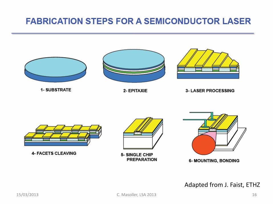
The development of SCLs and applications
• Lasing in semiconductor diodes was first observed in 1962 (pulsed operation, cryogenic temperatures), only two years after the first demonstration of a laser.
• Semiconductor lasers (SCLs or diode lasers) are electrically pumped, and convert electrical power into optical power.
• SCLs appeared in telecom networks in the 1970s, in compact disc players in the 1980s, and high-power diodes emerged in the 1990s for optical pumping, medicine, and materials processing.
• After 50 years, the diode laser market is over $3 billion, and
new technology and applications are still appearing.
15/03/2013 C. Masoller, LSA 2013 4
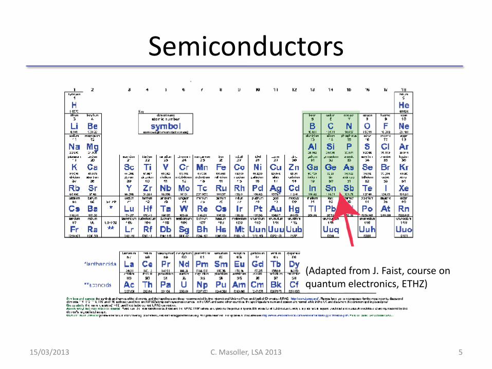
Semiconductors
15/03/2013 C. Masoller, LSA 2013 5
(Adapted from J. Faist, course on quantum electronics, ETHZ)
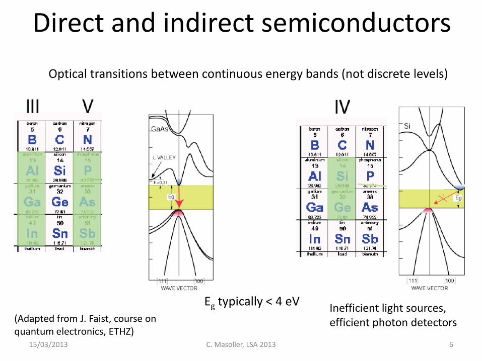
Direct and indirect semiconductors
15/03/2013 C. Masoller, LSA 2013 6
(Adapted from J. Faist, course on quantum electronics, ETHZ)
Inefficient light sources, efficient photon detectors
Optical transitions between continuous energy bands (not discrete levels)
Eg typically < 4 eV
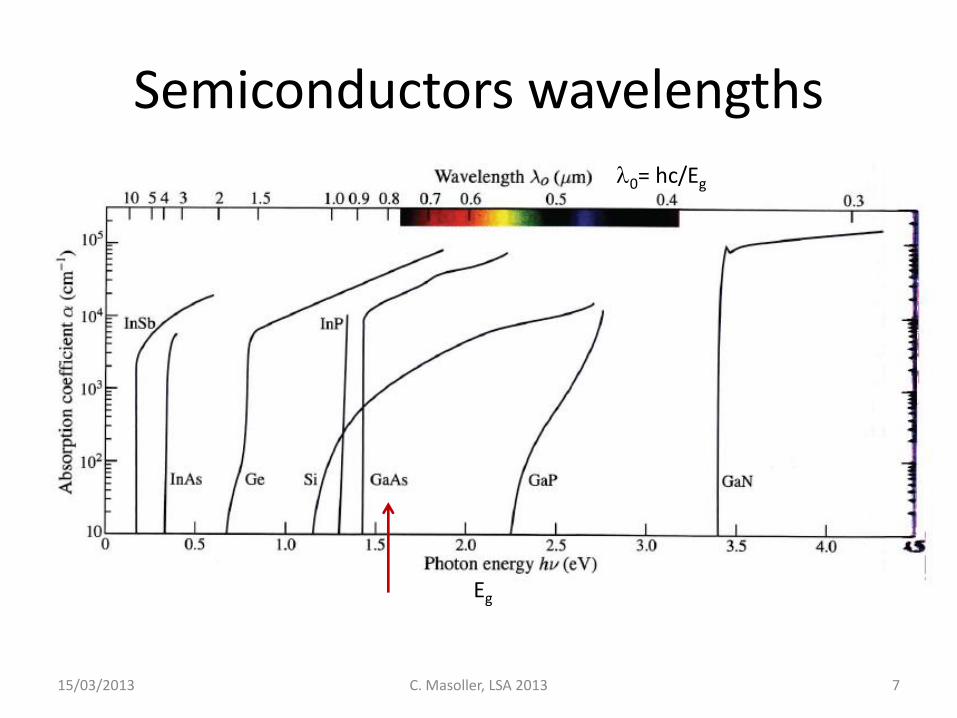
Semiconductors wavelengths
15/03/2013 C. Masoller, LSA 2013 7
0= hc/Eg
Eg
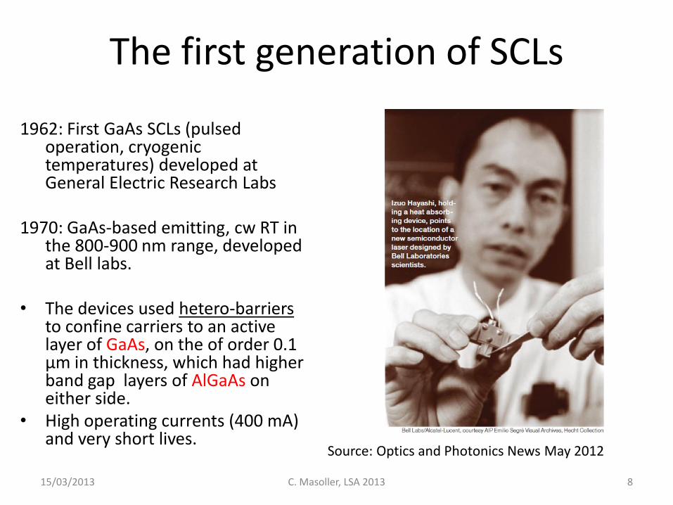
The first generation of SCLs
1962: First GaAs SCLs (pulsed operation, cryogenic temperatures) developed at General Electric Research Labs
1970: GaAs-based emitting, cw RT in
the 800-900 nm range, developed at Bell labs.
• The devices used hetero-barriers
to confine carriers to an active layer of GaAs, on the of order 0.1 μm in thickness, which had higher band gap layers of AlGaAs on either side.
• High operating currents (400 mA) and very short lives.
15/03/2013 C. Masoller, LSA 2013 8
Source: Optics and Photonics News May 2012
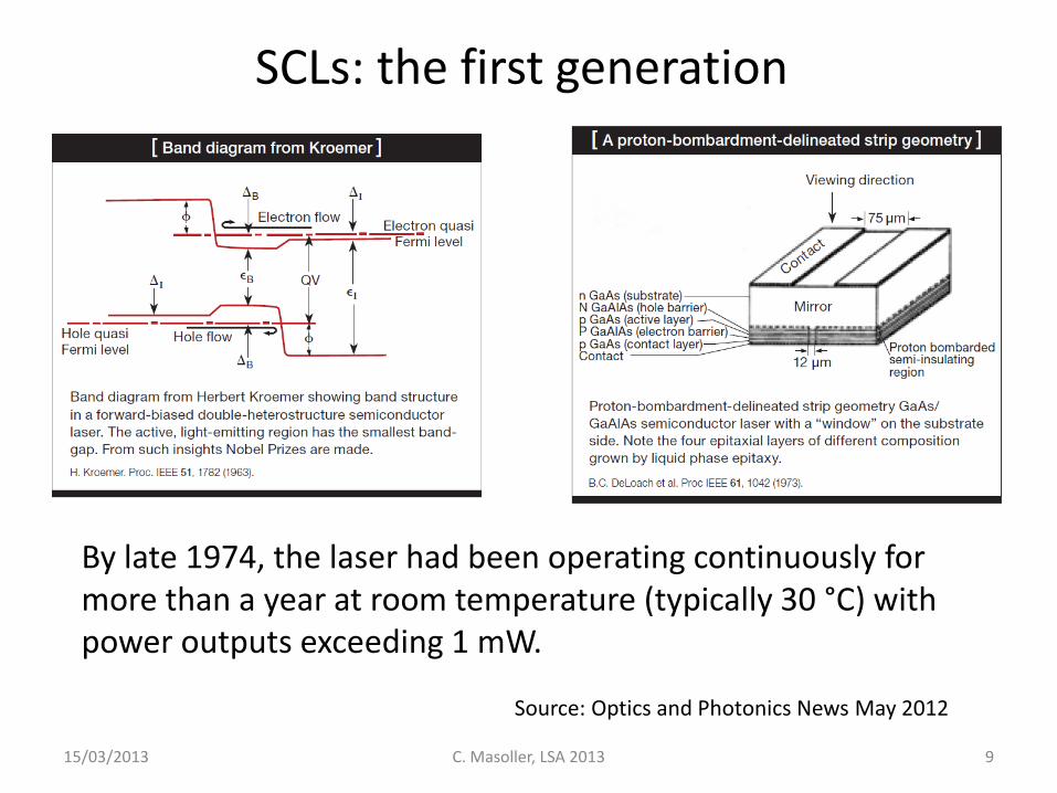
SCLs: the first generation
15/03/2013 C. Masoller, LSA 2013 9
By late 1974, the laser had been operating continuously for more than a year at room temperature (typically 30 °C) with power outputs exceeding 1 mW.
Source: Optics and Photonics News May 2012
Early applications
15/03/2013 C. Masoller, LSA 2013 10
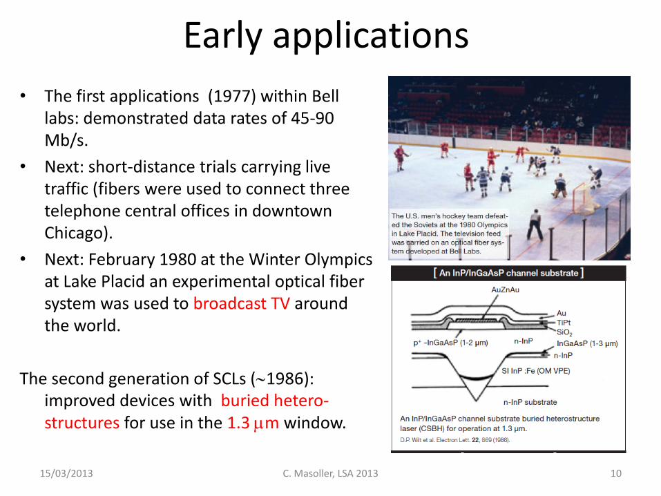
• The first applications (1977) within Bell labs: demonstrated data rates of 45-90 Mb/s.
• Next: short-distance trials carrying live traffic (fibers were used to connect three telephone central offices in downtown Chicago).
• Next: February 1980 at the Winter Olympics at Lake Placid an experimental optical fiber system was used to broadcast TV around the world.
The second generation of SCLs (1986): improved devices with buried hetero-structures for use in the 1.3 m window.
SCLs in communications: then to now • Today, all terrestrial and undersea
telecommunications, data and television traffic above the local distribution level is carried in fibers using SCLs as light sources.
• The Internet would not be possible without SC lasers.
• Continuously-wave (cw) operating lasers, which carry no signal information, are used to pump fiber amplifiers that are periodically spaced under the sea.
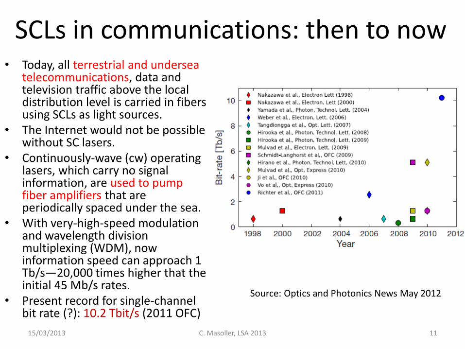
• With very-high-speed modulation and wavelength division multiplexing (WDM), now information speed can approach 1 Tb/s—20,000 times higher that the initial 45 Mb/s rates.
• Present record for single-channel bit rate (?): 10.2 Tbit/s (2011 OFC)
15/03/2013 C. Masoller, LSA 2013 11
Source: Optics and Photonics News May 2012
SCLs also in consumer products
15/03/2013 C. Masoller, LSA 2013 12
Printers, scanners, CD/DVD players, etc —a dramatic price reductions made possible these applications (the VCSEL in a computer mouse costs about 10 cents of US dollar to manufacture)
Source: Laserfocusworld.com
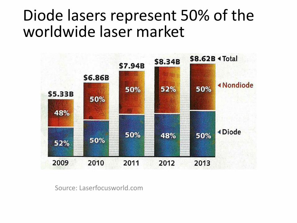
Diode lasers represent 50% of the worldwide laser market
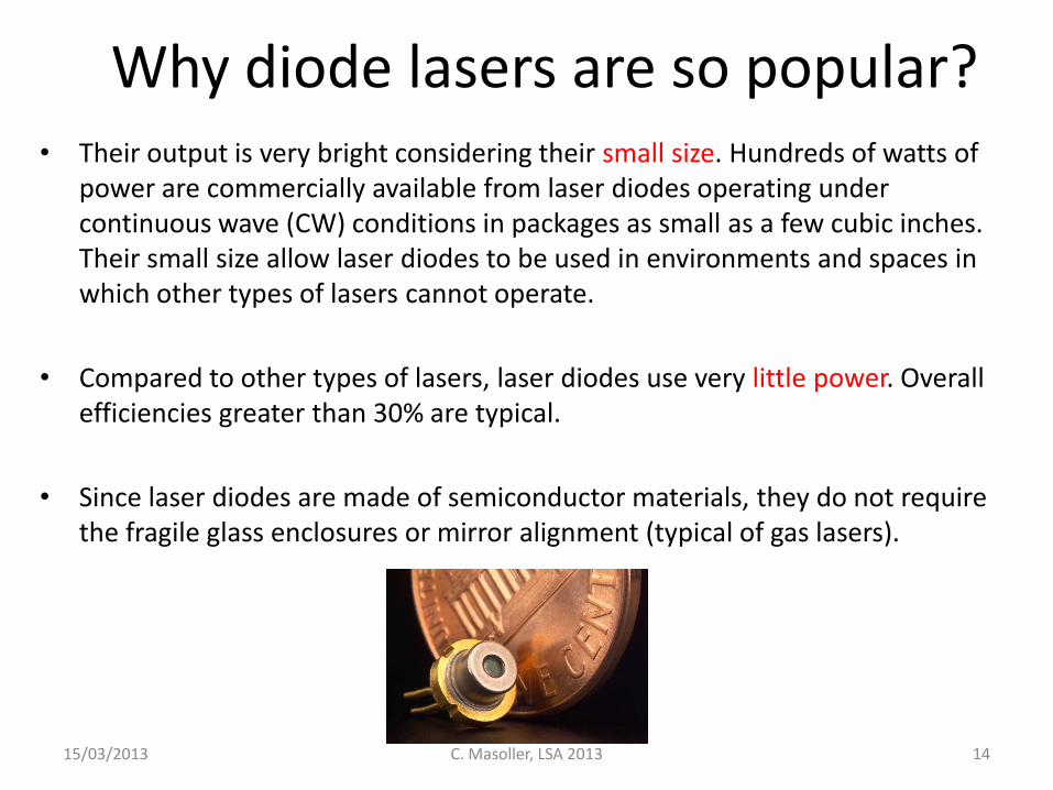
Why diode lasers are so popular? • Their output is very bright considering their small size. Hundreds of watts of
power are commercially available from laser diodes operating under continuous wave (CW) conditions in packages as small as a few cubic inches. Their small size allow laser diodes to be used in environments and spaces in which other types of lasers cannot operate.
• Compared to other types of lasers, laser diodes use very little power. Overall efficiencies greater than 30% are typical.
• Since laser diodes are made of semiconductor materials, they do not require the fragile glass enclosures or mirror alignment (typical of gas lasers).
15/03/2013 C. Masoller, LSA 2013 14
Also popular because
• Coherence and single wavelength characteristics of laser diodes enable the outputs of these devices to be focused to a diffraction limited spot size. The size of the resultant spot is dependent on the wavelength of the laser - the shorter the wavelength of light, the smaller the size of the spot.
• Operation at shorter blue and UV wavelengths makes smaller spot sizes possible, allowing more information to be stored on optical disks at a higher density.
• They can be directly modulated at high frequencies. By modulating the drive current, the laser output is modulated at GHz frequencies in high-speed data communications.
15/03/2013 C. Masoller, LSA 2013 15
15/03/2013 C. Masoller, LSA 2013 16
Adapted from J. Faist, ETHZ
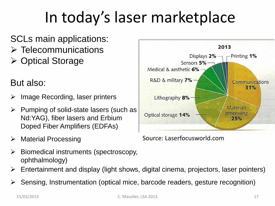
In today’s laser marketplace
15/03/2013 17 C. Masoller, LSA 2013
SCLs main applications:
Telecommunications
Optical Storage
But also:
Image Recording, laser printers
Pumping of solid-state lasers (such as
Nd:YAG), fiber lasers and Erbium
Doped Fiber Amplifiers (EDFAs)
Material Processing
Biomedical instruments (spectroscopy,
ophthalmology)
Source: Laserfocusworld.com
Entertainment and display (light shows, digital cinema, projectors, laser pointers)
Sensing, Instrumentation (optical mice, barcode readers, gesture recognition)
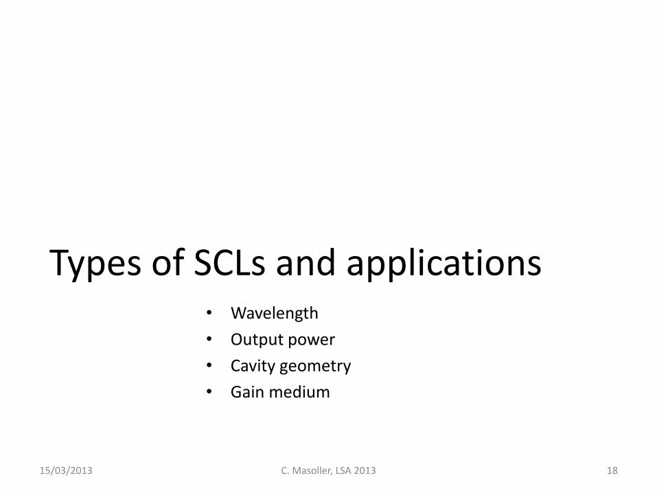
Types of SCLs and applications • Wavelength
• Output power
• Cavity geometry
• Gain medium
15/03/2013 C. Masoller, LSA 2013 18
Wavelengths
15/03/2013 19 C. Masoller, LSA 2013
Short wavelength
• λ= 635 - 980 nm
• Fabrication by epitaxial growth on gallium arsenide (GaAs) substrates
• Optical data storage
Long wavelength
• λ= 980 - 1550 nm
• Fabrication by epitaxial growth on indium phosphide (InP) substrates
• Telecom
= 980 nm Pumping of Erbium Doped Fiber Amplifiers (EDFAs)
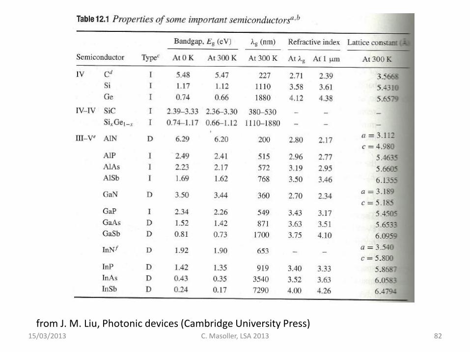
Band-gap energy and wavelength of semiconductor materials
15/03/2013 C. Masoller, LSA 2013 20
Blue laser diodes are based on gallium nitride (GaN) or indium gallium nitride (InGaN) technologies.
Blue lasers can also be constructed using frequency-doubling of infrared laser wavelengths.
SUEMATSU & IGA: SEMICONDUCTOR LASERS IN PHOTONICS, JOURNAL OF LIGHTWAVE TECHNOLOGY,
VOL. 26, NO. 9, MAY 1, 2008
Optical data storage
• Has led to revolutionary advances in information processing. • One of the key challenges is to meet the demand for storage
capacity. • ‘Bit-by-bit’ optical data storage systems are
– compact discs (CDs) – digital video discs (DVDs) – Blu-ray discs (Blu-rays)
• Advantages – compact and portable devices (high tolerance to vibrations) – high memory density – high resistance to intense electromagnetic radiation.
• Key advantages with respect to holographic data storage systems (capable recording and reading millions of bits in parallel)
15/03/2013 C. Masoller, LSA 2013 21
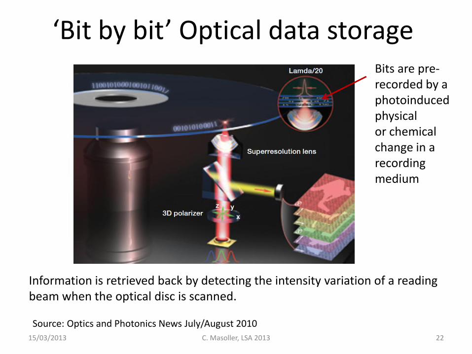
‘Bit by bit’ Optical data storage
15/03/2013 C. Masoller, LSA 2013 22
Bits are pre-recorded by a photoinduced physical or chemical change in a recording medium
Information is retrieved back by detecting the intensity variation of a reading beam when the optical disc is scanned.
Source: Optics and Photonics News July/August 2010
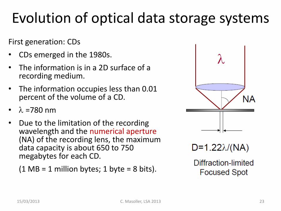
Evolution of optical data storage systems
First generation: CDs
• CDs emerged in the 1980s.
• The information is in a 2D surface of a recording medium.
• The information occupies less than 0.01 percent of the volume of a CD.
• =780 nm
• Due to the limitation of the recording wavelength and the numerical aperture (NA) of the recording lens, the maximum data capacity is about 650 to 750 megabytes for each CD.
(1 MB = 1 million bytes; 1 byte = 8 bits).
15/03/2013 C. Masoller, LSA 2013 23
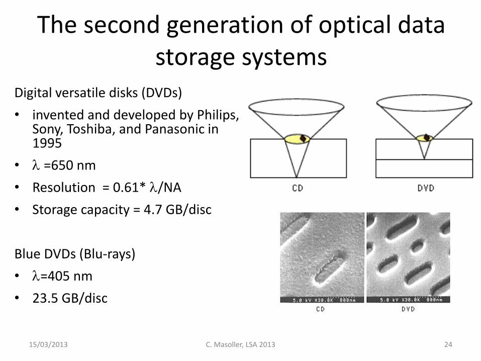
The second generation of optical data storage systems
Digital versatile disks (DVDs)
• invented and developed by Philips, Sony, Toshiba, and Panasonic in 1995
• =650 nm
• Resolution = 0.61* /NA
• Storage capacity = 4.7 GB/disc
Blue DVDs (Blu-rays)
• =405 nm
• 23.5 GB/disc
15/03/2013 C. Masoller, LSA 2013 24
15/03/2013 C. Masoller, LSA 2013 25
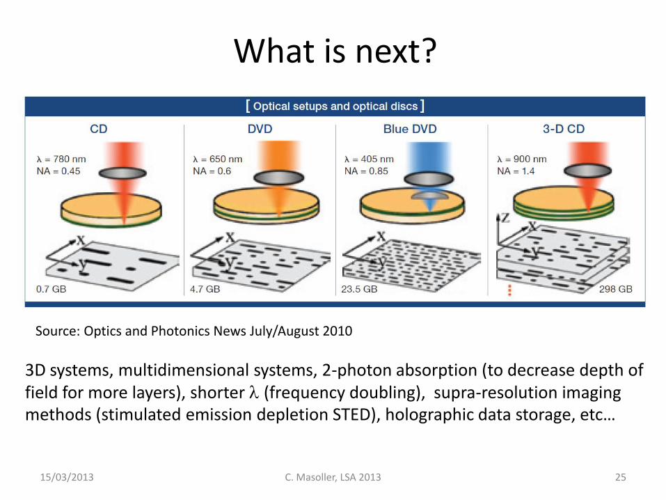
What is next?
Source: Optics and Photonics News July/August 2010
3D systems, multidimensional systems, 2-photon absorption (to decrease depth of field for more layers), shorter (frequency doubling), supra-resolution imaging methods (stimulated emission depletion STED), holographic data storage, etc…
15/03/2013 C. Masoller, LSA 2013 26
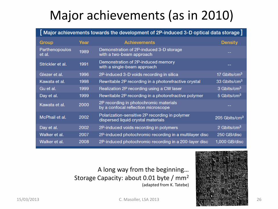
Major achievements (as in 2010)
A long way from the beginning… Storage Capacity: about 0.01 byte / mm2
(adapted from K. Tatebe)
SCLs in optical communications
15/03/2013 C. Masoller, LSA 2013 27
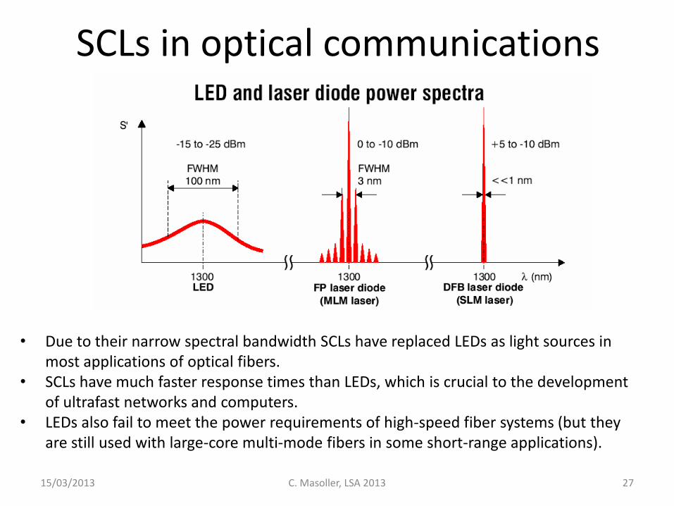
• Due to their narrow spectral bandwidth SCLs have replaced LEDs as light sources in most applications of optical fibers.
• SCLs have much faster response times than LEDs, which is crucial to the development of ultrafast networks and computers.
• LEDs also fail to meet the power requirements of high-speed fiber systems (but they are still used with large-core multi-mode fibers in some short-range applications).
Telecom wavelengths
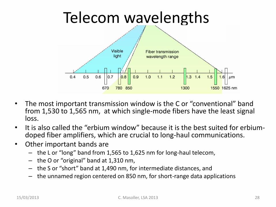
• The most important transmission window is the C or “conventional” band from 1,530 to 1,565 nm, at which single-mode fibers have the least signal loss.
• It is also called the “erbium window” because it is the best suited for erbium-doped fiber amplifiers, which are crucial to long-haul communications.
• Other important bands are – the L or “long” band from 1,565 to 1,625 nm for long-haul telecom, – the O or “original” band at 1,310 nm, – the S or “short” band at 1,490 nm, for intermediate distances, and – the unnamed region centered on 850 nm, for short-range data applications
15/03/2013 C. Masoller, LSA 2013 28
15/03/2013 C. Masoller, LSA 2013 29
• Over the past 20 years tunable SCLs have been developed, whose operating wavelength can be adjusted within the relevant communications band.
• The SCLs used in optical communications are Distributed Feedback lasers (DFBs) and vertical-cavity surface-emitting lasers (VCSELs), more latter.
• The lasers must send out a signal within the optimum
transmission windows of the fibers with enough power to reach the receiver or repeater with a sufficient signal-to-noise ratio (but not so much as to create undesirable nonlinearities).
SCLs in optical communications
The different types of networks have their own requirements for semiconductor lasers and modulation schemes. • Long-haul (telecommunications, > 100 km),
• Metropolitan ( 10 km),
• Access (communications links between subscribers and their telecom or
datacom service provider: the link to your Internet, cable-television and/or phone company: “fiber to the home” or FTTH, < 10 km)
• Interconnects (of short-haul data communications or datacom < 100 m)
15/03/2013 30 C. Masoller, LSA 2013
SCLs in optical communications
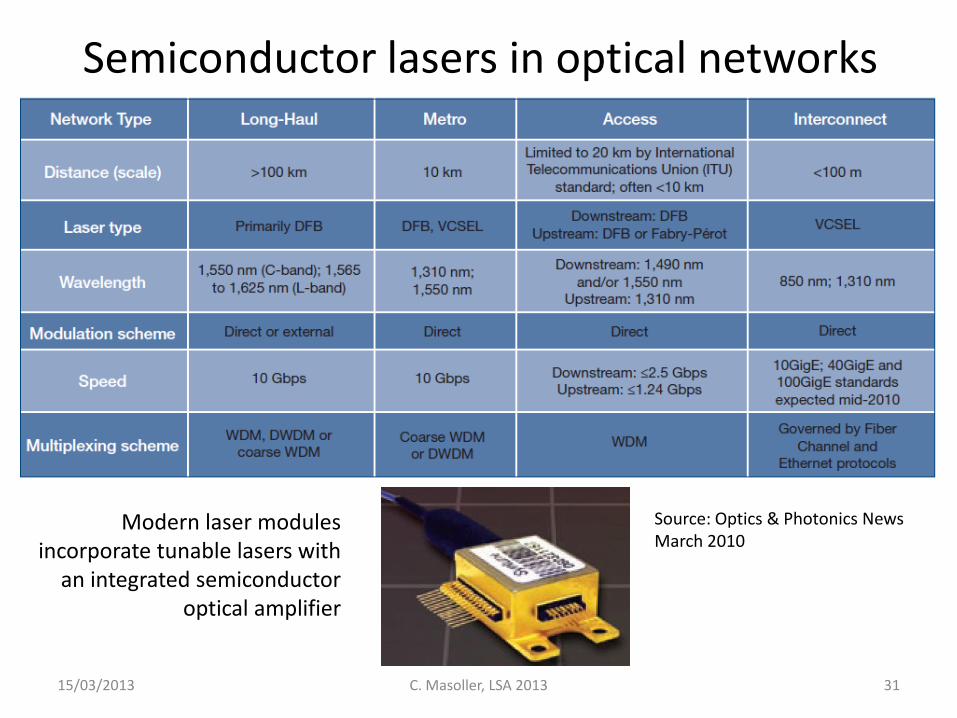
Semiconductor lasers in optical networks
Source: Optics & Photonics News March 2010
15/03/2013 31 C. Masoller, LSA 2013
Modern laser modules incorporate tunable lasers with
an integrated semiconductor optical amplifier
Wavelength division multiplexing (WDM)
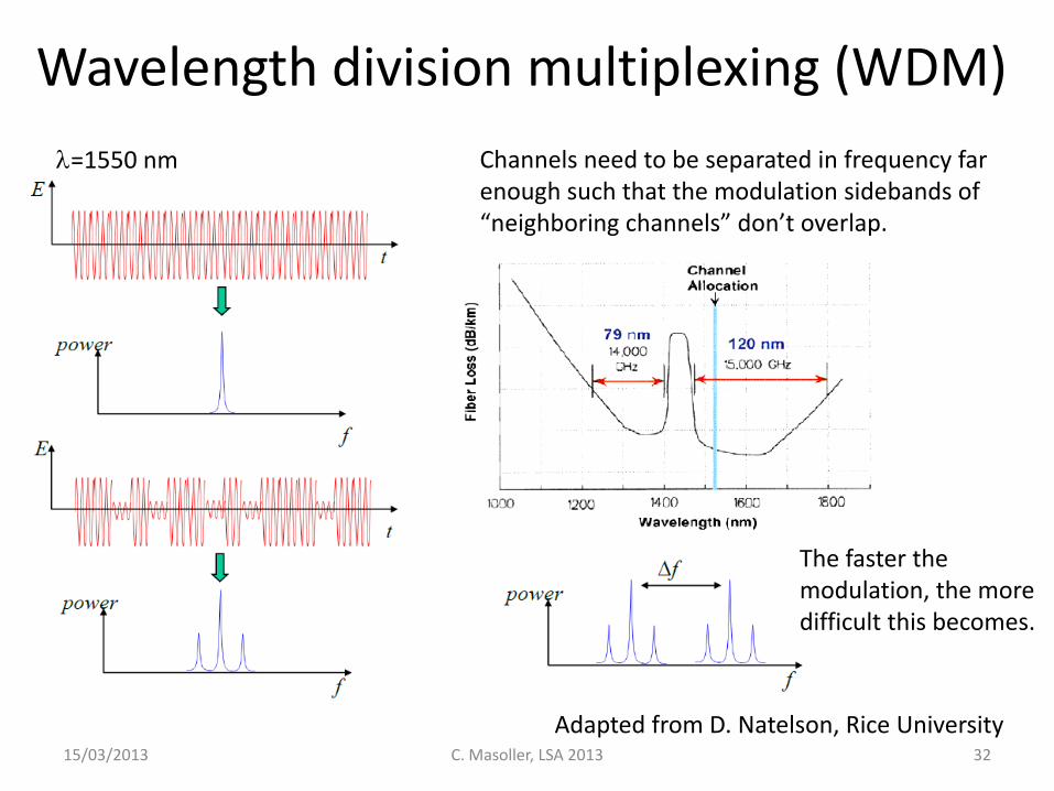
15/03/2013 C. Masoller, LSA 2013 32
=1550 nm Channels need to be separated in frequency far enough such that the modulation sidebands of “neighboring channels” don’t overlap.
The faster the modulation, the more difficult this becomes.
Adapted from D. Natelson, Rice University
15/03/2013 C. Masoller, LSA 2013 33
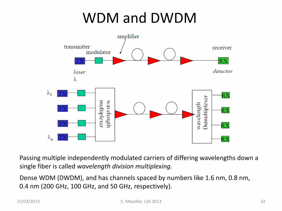
Passing multiple independently modulated carriers of differing wavelengths down a single fiber is called wavelength division multiplexing.
WDM and DWDM
Dense WDM (DWDM), and has channels spaced by numbers like 1.6 nm, 0.8 nm, 0.4 nm (200 GHz, 100 GHz, and 50 GHz, respectively).
Types of SCLs and applications • Wavelength
• Output power
• Cavity geometry
• Gain medium
15/03/2013 C. Masoller, LSA 2013 34
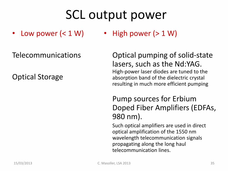
SCL output power • Low power (< 1 W)
Telecommunications
Optical Storage
• High power (> 1 W)
Optical pumping of solid-state lasers, such as the Nd:YAG. High-power laser diodes are tuned to the absorption band of the dielectric crystal resulting in much more efficient pumping
Pump sources for Erbium Doped Fiber Amplifiers (EDFAs, 980 nm).
Such optical amplifiers are used in direct optical amplification of the 1550 nm wavelength telecommunication signals propagating along the long haul telecommunication lines.
15/03/2013 C. Masoller, LSA 2013 35
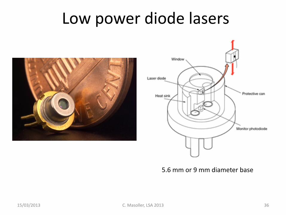
Low power diode lasers
15/03/2013 C. Masoller, LSA 2013 36
5.6 mm or 9 mm diameter base
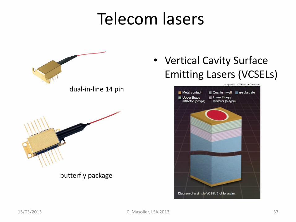
Telecom lasers
• Vertical Cavity Surface Emitting Lasers (VCSELs)
15/03/2013 C. Masoller, LSA 2013 37
butterfly package
dual-in-line 14 pin
15/03/2013 C. Masoller, LSA 2013 38
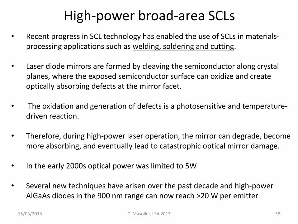
High-power broad-area SCLs • Recent progress in SCL technology has enabled the use of SCLs in materials-
processing applications such as welding, soldering and cutting.
• Laser diode mirrors are formed by cleaving the semiconductor along crystal planes, where the exposed semiconductor surface can oxidize and create optically absorbing defects at the mirror facet.
• The oxidation and generation of defects is a photosensitive and temperature-driven reaction.
• Therefore, during high-power laser operation, the mirror can degrade, become more absorbing, and eventually lead to catastrophic optical mirror damage.
• In the early 2000s optical power was limited to 5W
• Several new techniques have arisen over the past decade and high-power AlGaAs diodes in the 900 nm range can now reach >20 W per emitter
15/03/2013 C. Masoller, LSA 2013 39
Optics and Photonics News, October 2010
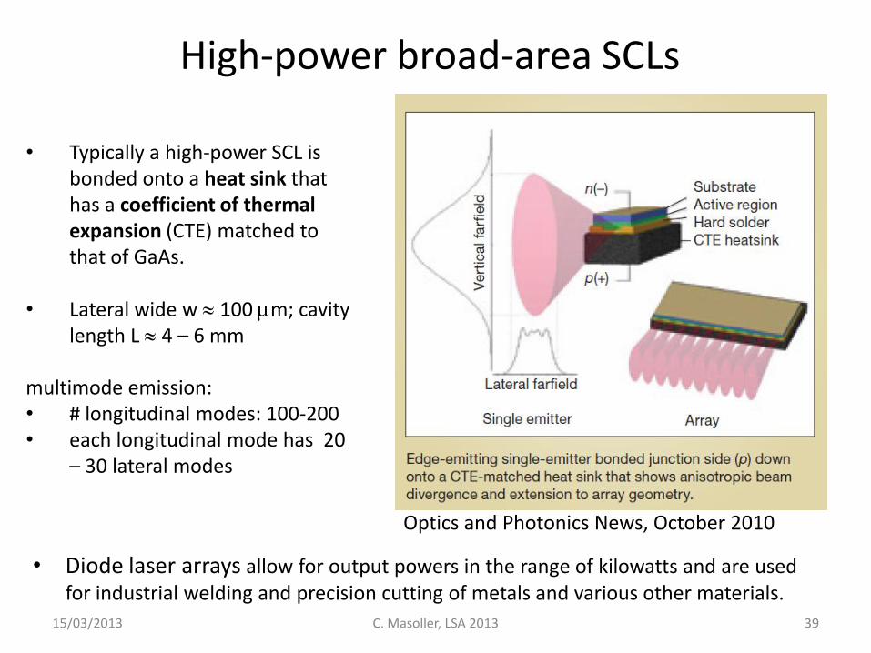
• Typically a high-power SCL is bonded onto a heat sink that has a coefficient of thermal expansion (CTE) matched to that of GaAs.
• Lateral wide w 100 m; cavity
length L 4 – 6 mm multimode emission: • # longitudinal modes: 100-200 • each longitudinal mode has 20
– 30 lateral modes
High-power broad-area SCLs
• Diode laser arrays allow for output powers in the range of kilowatts and are used for industrial welding and precision cutting of metals and various other materials.
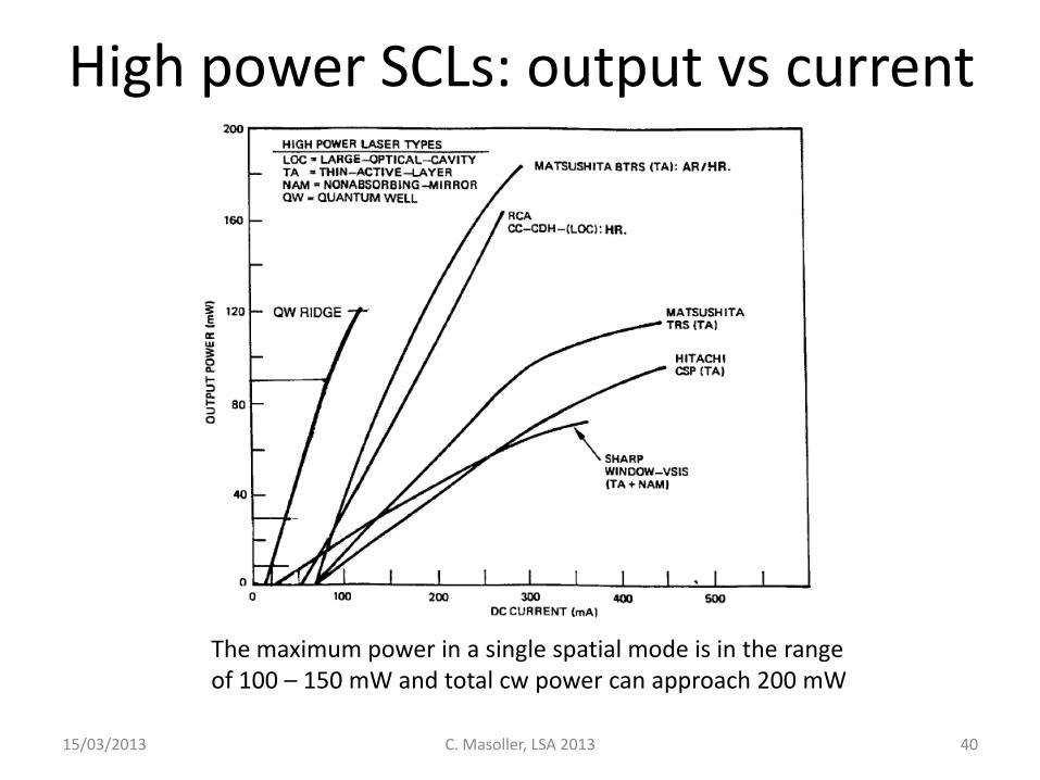
High power SCLs: output vs current
15/03/2013 C. Masoller, LSA 2013 40
The maximum power in a single spatial mode is in the range of 100 – 150 mW and total cw power can approach 200 mW

Types of SCLs and applications • Wavelength
• Output power
• Cavity geometry
• Gain medium
15/03/2013 C. Masoller, LSA 2013 41
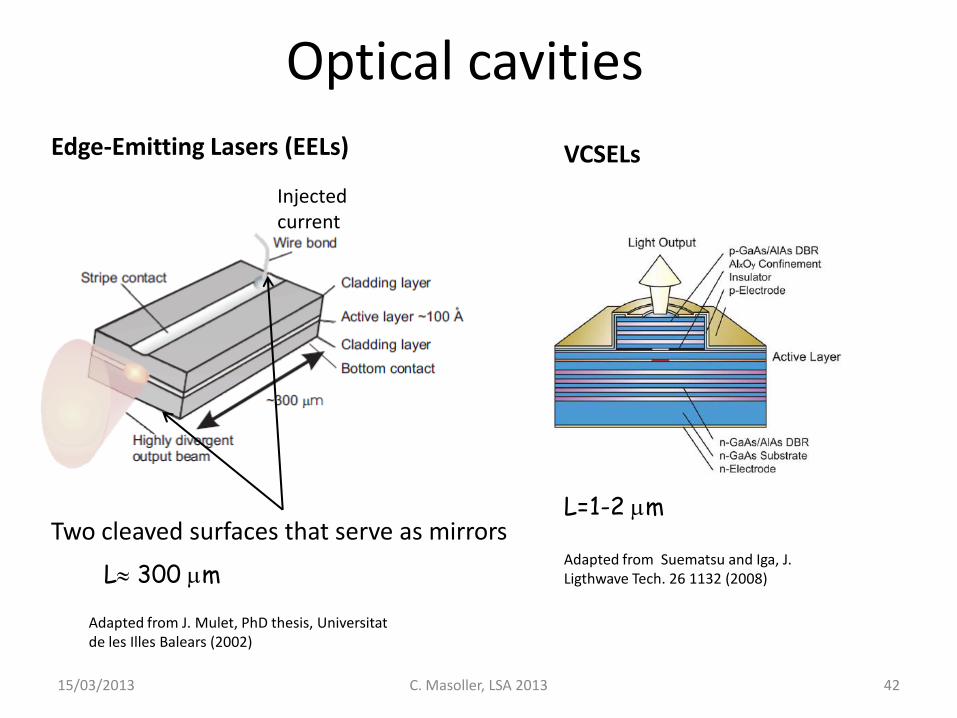
Optical cavities
Edge-Emitting Lasers (EELs) VCSELs
Two cleaved surfaces that serve as mirrors
Injected current
L=1-2 m Adapted from Suematsu and Iga, J. Ligthwave Tech. 26 1132 (2008)
Adapted from J. Mulet, PhD thesis, Universitat de les Illes Balears (2002)
15/03/2013 42 C. Masoller, LSA 2013
L 300 m
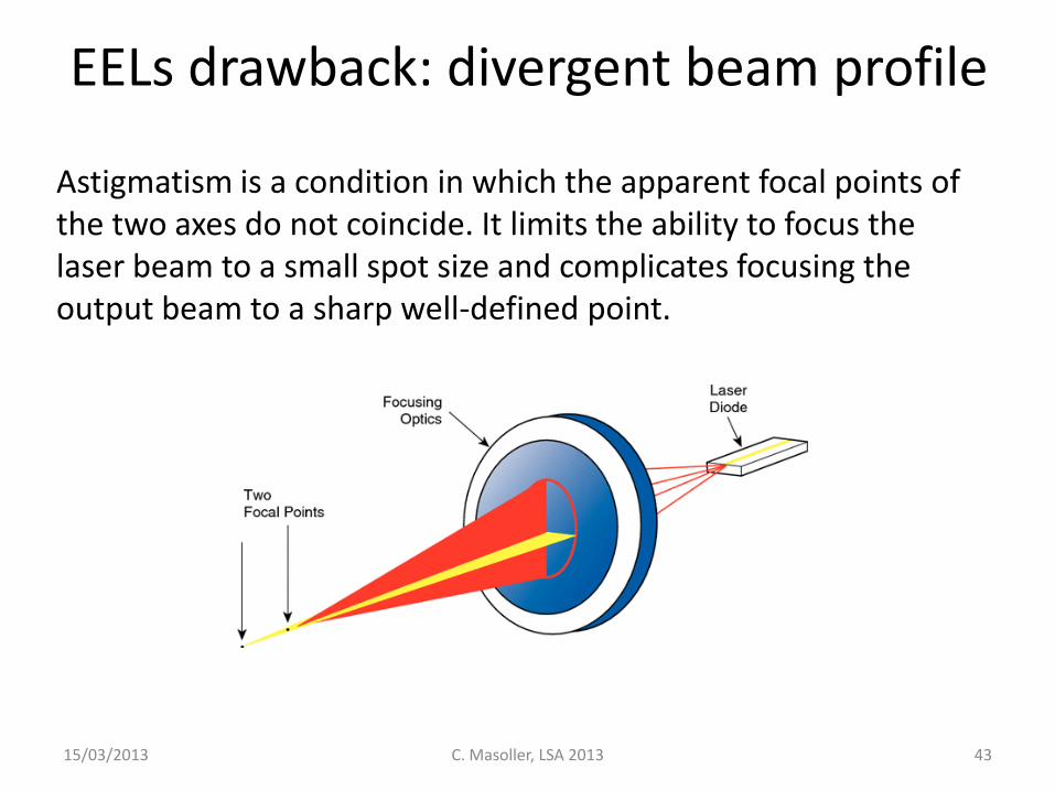
EELs drawback: divergent beam profile
15/03/2013 C. Masoller, LSA 2013 43
Astigmatism is a condition in which the apparent focal points of the two axes do not coincide. It limits the ability to focus the laser beam to a small spot size and complicates focusing the output beam to a sharp well-defined point.
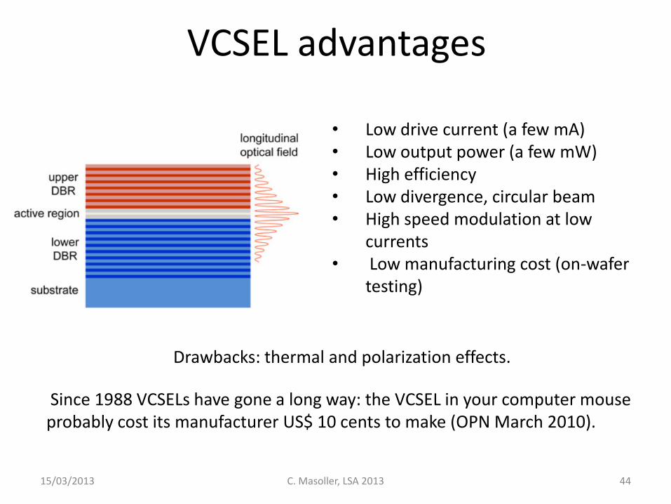
VCSEL advantages
• Low drive current (a few mA) • Low output power (a few mW) • High efficiency • Low divergence, circular beam • High speed modulation at low
currents • Low manufacturing cost (on-wafer
testing)
Since 1988 VCSELs have gone a long way: the VCSEL in your computer mouse probably cost its manufacturer US$ 10 cents to make (OPN March 2010).
15/03/2013 44 C. Masoller, LSA 2013
Drawbacks: thermal and polarization effects.
VCSEL advantages
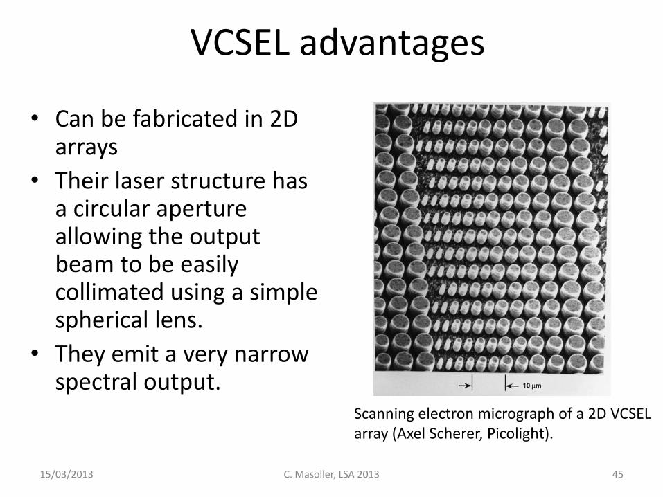
• Can be fabricated in 2D arrays
• Their laser structure has a circular aperture allowing the output beam to be easily collimated using a simple spherical lens.
• They emit a very narrow spectral output.
15/03/2013 C. Masoller, LSA 2013 45
Scanning electron micrograph of a 2D VCSEL array (Axel Scherer, Picolight).
15/03/2013 46 C. Masoller, LSA 2013
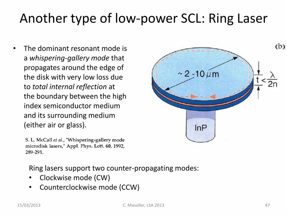
• The dominant resonant mode is a whispering-gallery mode that propagates around the edge of the disk with very low loss due to total internal reflection at the boundary between the high index semiconductor medium and its surrounding medium (either air or glass).
Another type of low-power SCL: Ring Laser
15/03/2013 47 C. Masoller, LSA 2013
Ring lasers support two counter-propagating modes: • Clockwise mode (CW) • Counterclockwise mode (CCW)
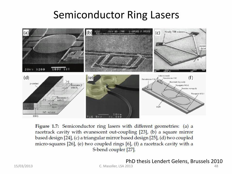
Semiconductor Ring Lasers
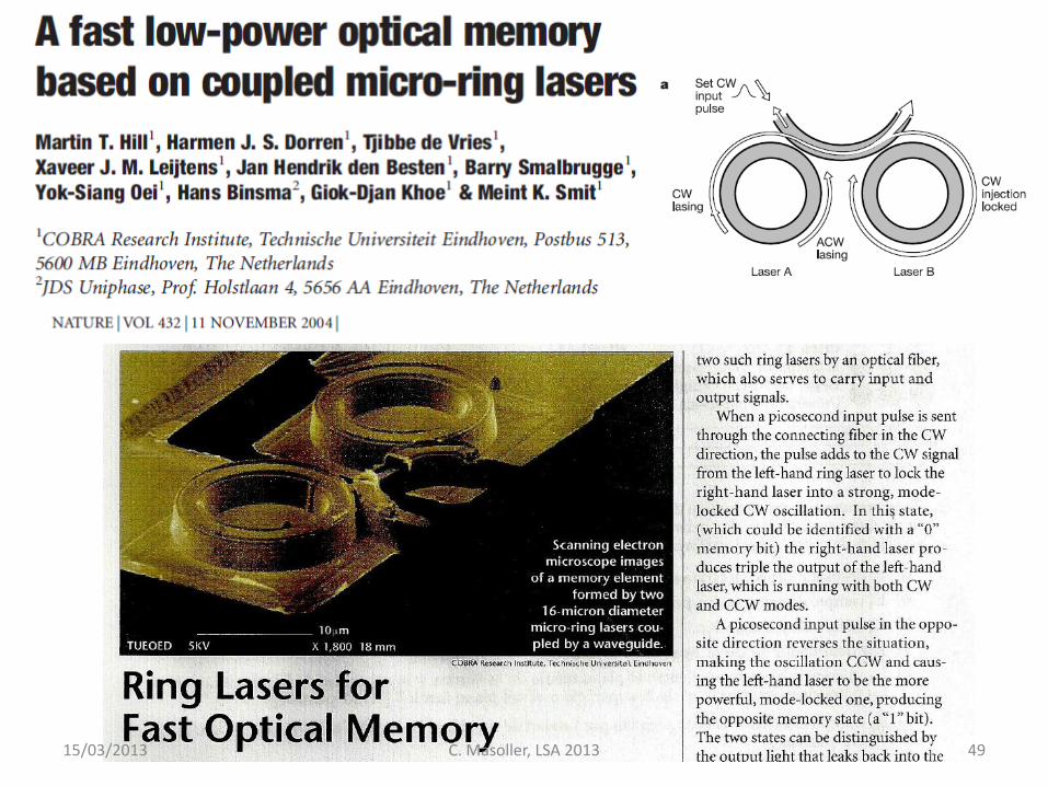
PhD thesis Lendert Gelens, Brussels 2010 15/03/2013 48 C. Masoller, LSA 2013
15/03/2013 49 C. Masoller, LSA 2013
15/03/2013 C. Masoller, LSA 2013 50
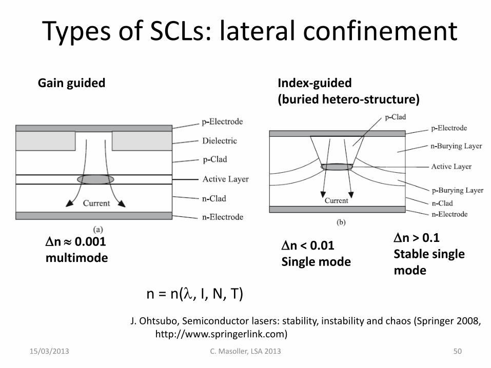
Gain guided Index-guided (buried hetero-structure)
n 0.001 multimode
n < 0.01 Single mode
n > 0.1 Stable single mode
n = n(, I, N, T)
J. Ohtsubo, Semiconductor lasers: stability, instability and chaos (Springer 2008, http://www.springerlink.com)
Types of SCLs: lateral confinement
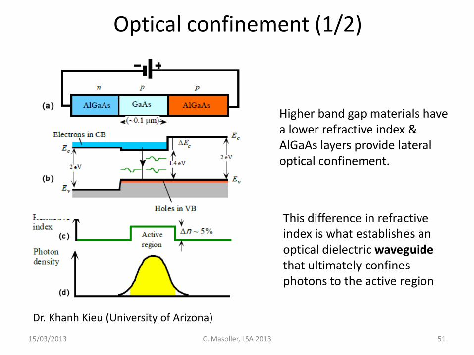
Optical confinement (1/2)
Higher band gap materials have a lower refractive index & AlGaAs layers provide lateral optical confinement.
This difference in refractive index is what establishes an optical dielectric waveguide that ultimately confines photons to the active region
15/03/2013 51 C. Masoller, LSA 2013
Dr. Khanh Kieu (University of Arizona)
15/03/2013 C. Masoller, LSA 2013 52
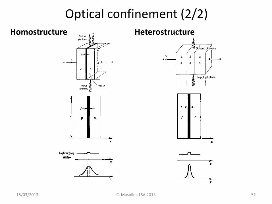
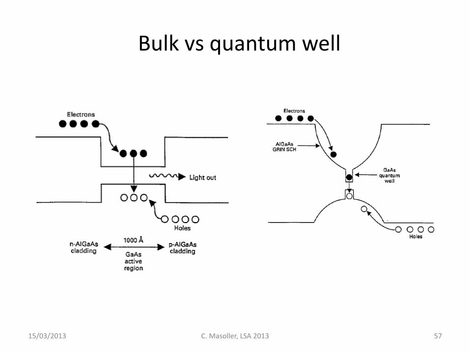
Optical confinement (2/2) Heterostructure Homostructure
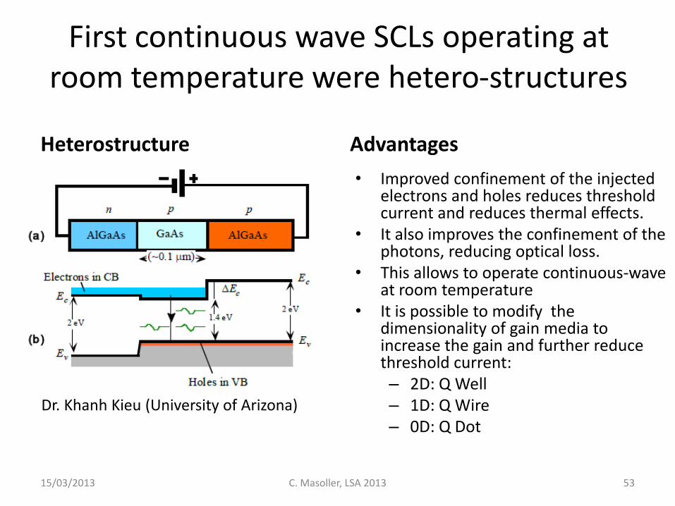
First continuous wave SCLs operating at room temperature were hetero-structures
Heterostructure Advantages
• Improved confinement of the injected electrons and holes reduces threshold current and reduces thermal effects.
• It also improves the confinement of the photons, reducing optical loss.
• This allows to operate continuous-wave at room temperature
• It is possible to modify the dimensionality of gain media to increase the gain and further reduce threshold current: – 2D: Q Well – 1D: Q Wire – 0D: Q Dot
15/03/2013 53 C. Masoller, LSA 2013
Dr. Khanh Kieu (University of Arizona)
Heterostructures
The 2000 Nobel Prize in Physics was awarded
"for basic work on information and communication technology"
with one half jointly to Zhores I. Alferov (Iaffe Physico-Technical Institute, St. Petersburg, Russia) and Herbert Kroemer (University of California, USA)
"for developing semiconductor heterostructures used in high-speed- and opto-electronics"
15/03/2013 54 C. Masoller, LSA 2013
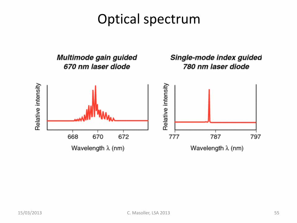
Optical spectrum
15/03/2013 55 C. Masoller, LSA 2013
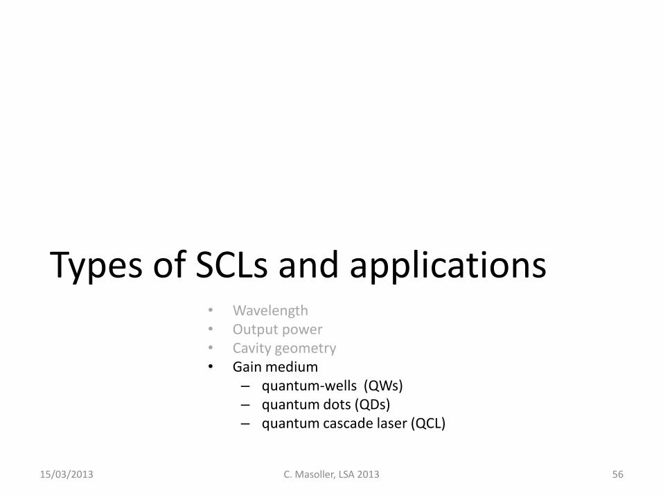
Types of SCLs and applications • Wavelength • Output power • Cavity geometry • Gain medium
– quantum-wells (QWs) – quantum dots (QDs) – quantum cascade laser (QCL)
15/03/2013 C. Masoller, LSA 2013 56
Bulk vs quantum well
15/03/2013 C. Masoller, LSA 2013 57
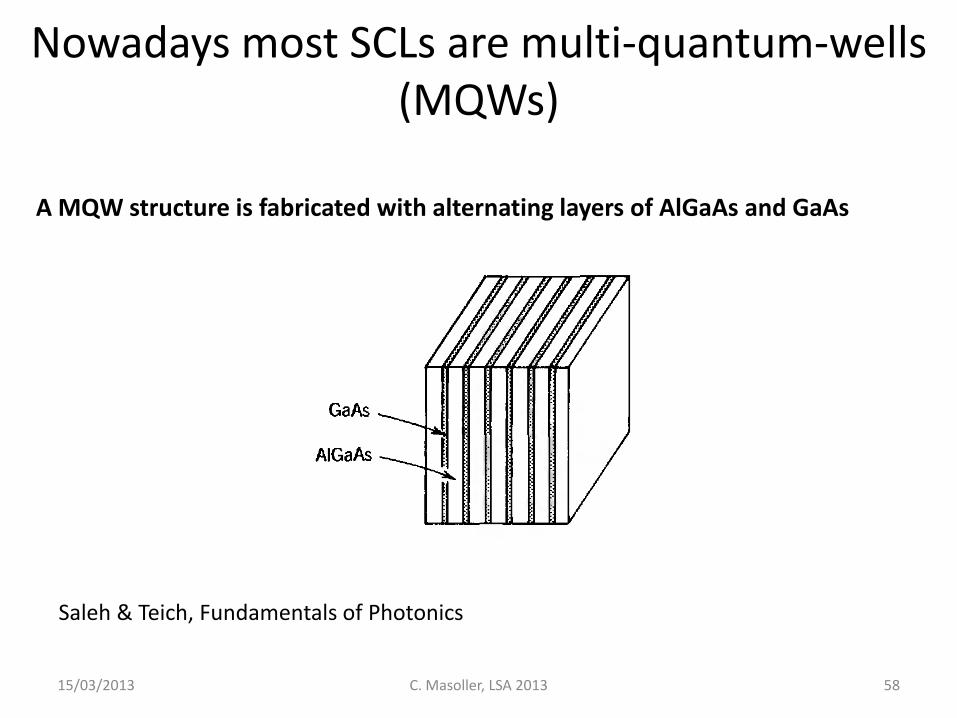
Nowadays most SCLs are multi-quantum-wells (MQWs)
A MQW structure is fabricated with alternating layers of AlGaAs and GaAs
Saleh & Teich, Fundamentals of Photonics
15/03/2013 58 C. Masoller, LSA 2013

Quantum dot lasers (QDLs)
• While quantum wells are essentially thin layers of active material, quantum dots are (as the name suggests), dots or islands of material surrounded by another material.
• The dots have a lower-energy bandgap than the surrounding material.
• Because they possess very different structures, QW and QD lasers can have very different properties even though they may be made from the same materials (such as InAs and GaAs).
15/03/2013 C. Masoller, LSA 2013 59
QDL wavelengths
• The natural wavelength of bulk GaAs is 870 nm. To achieve longer wavelengths (for example, 980nm) an increasing amount of indium has to be added to the quantum-well structure.
• As indium is a large atom, a lot of stress is induced in the layer and a limit is reached at around 1,100 nm.
• Because quantum dots are not layers, but islands, they may accommodate more strain, so more indium can be introduced, leading to a longer wavelength.
15/03/2013 C. Masoller, LSA 2013 60
QDL Tunability
• The lasing wavelength is determined by the size of the quantum dots.
• By controlling the size distribution of the quantum dots, QDLs offer a broad lasing spectrum.
• The tunability offered by changing the size and shape of the QDs allows these devices to reach wavelengths that are unachievable through other semiconductor laser technologies.
• This makes them ideal as a source for optical clock technology in optical computing.
15/03/2013 C. Masoller, LSA 2013 61
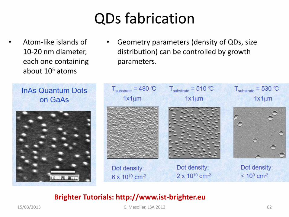
QDs fabrication
• Geometry parameters (density of QDs, size distribution) can be controlled by growth parameters.
15/03/2013 C. Masoller, LSA 2013 62
• Atom-like islands of 10-20 nm diameter, each one containing about 105 atoms
Brighter Tutorials: http://www.ist-brighter.eu
15/03/2013 63 Optics and Photonics News, July/August 2008
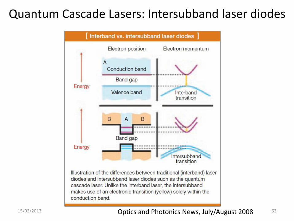
Quantum Cascade Lasers: Intersubband laser diodes
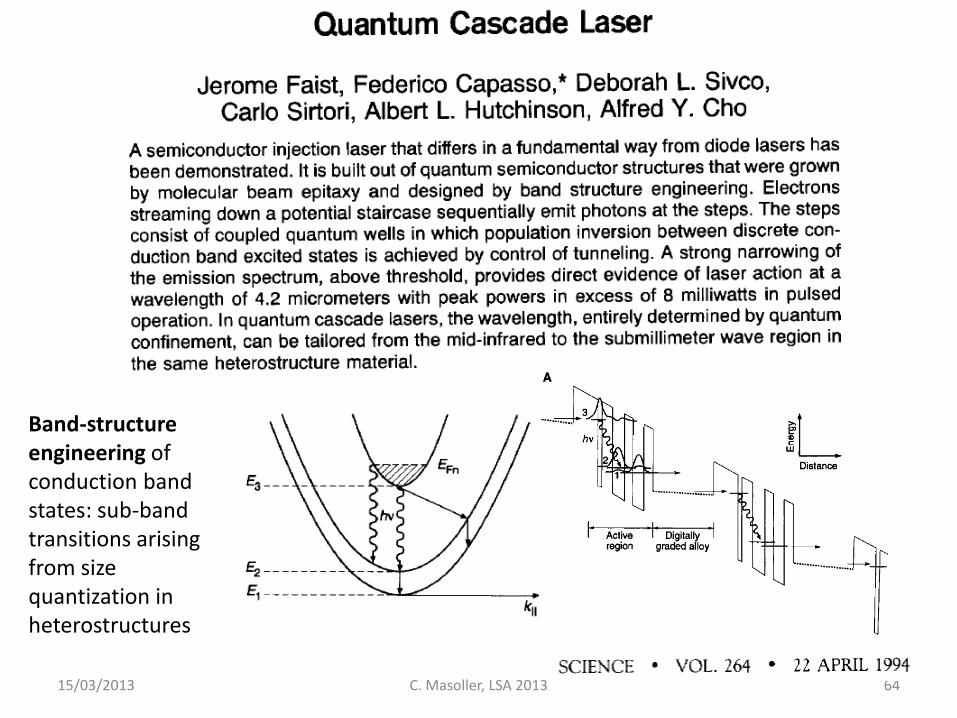
15/03/2013 C. Masoller, LSA 2013 64
Band-structure engineering of conduction band states: sub-band transitions arising from size quantization in heterostructures
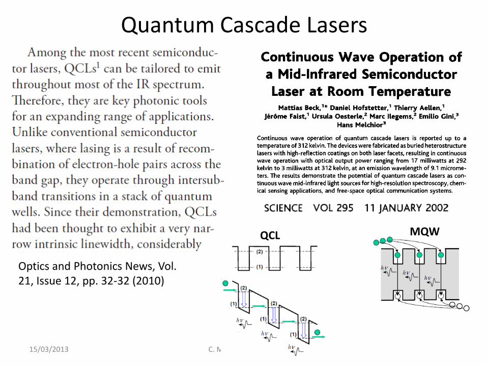
Quantum Cascade Lasers
Optics and Photonics News, Vol. 21, Issue 12, pp. 32-32 (2010)
15/03/2013 65 C. Masoller, LSA 2013
QCL MQW
15/03/2013 C. Masoller, LSA 2013 66
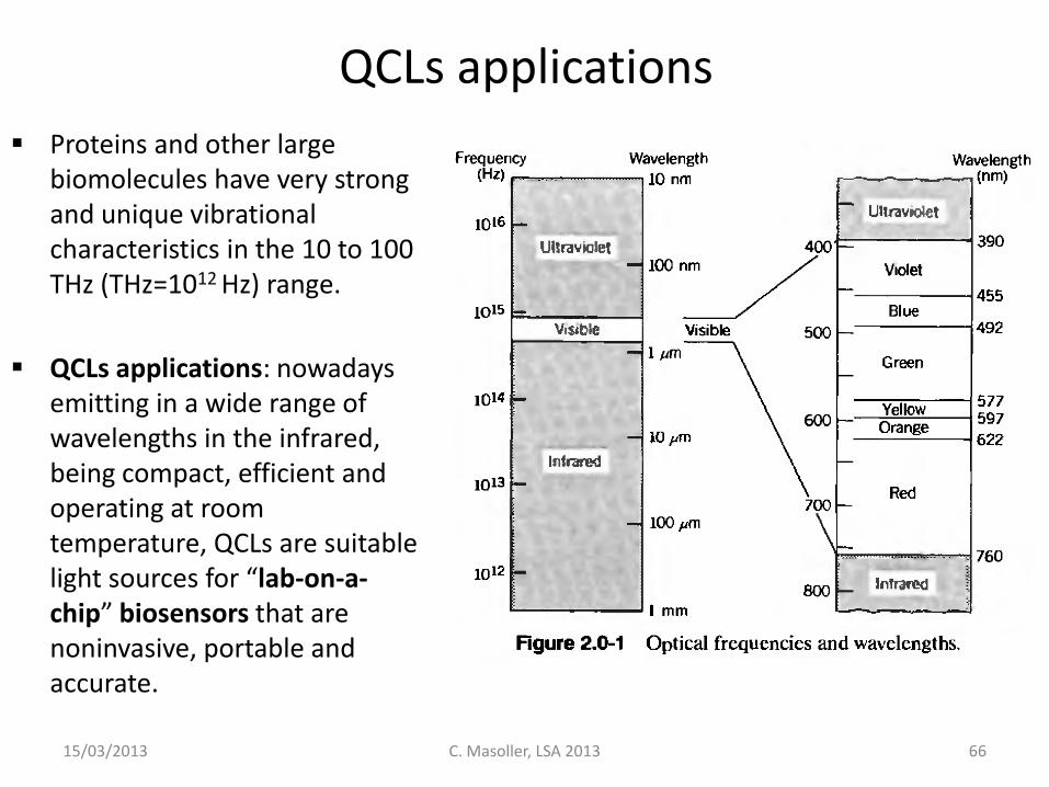
QCLs applications
Proteins and other large biomolecules have very strong and unique vibrational characteristics in the 10 to 100 THz (THz=1012 Hz) range.
QCLs applications: nowadays emitting in a wide range of wavelengths in the infrared, being compact, efficient and operating at room temperature, QCLs are suitable light sources for “lab-on-a-chip” biosensors that are noninvasive, portable and accurate.
15/03/2013 C. Masoller, LSA 2013 67
Optics and Photonics News, July/August 2008
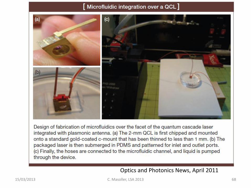
15/03/2013 C. Masoller, LSA 2013 68
Optics and Photonics News, April 2011
Summary
• By engineering the band gaps of semiconductor materials, laser emission can be obtained in a wide range of wavelengths (from mm –THz to ultraviolet).
• A variety of optical cavity structures leads to a variety of semiconductor laser devices.
• Key advantages are their inexpensive fabrication, and they are compact and reliable.
15/03/2013 C. Masoller, LSA 2013 69
3. Opto-Electronic Characteristics
• Output Light vs. Input Current Curve (L.I. Curve) • Longitudinal modes and optical spectrum • Lateral and transverse modes
15/03/2013 C. Masoller, LSA 2013 70
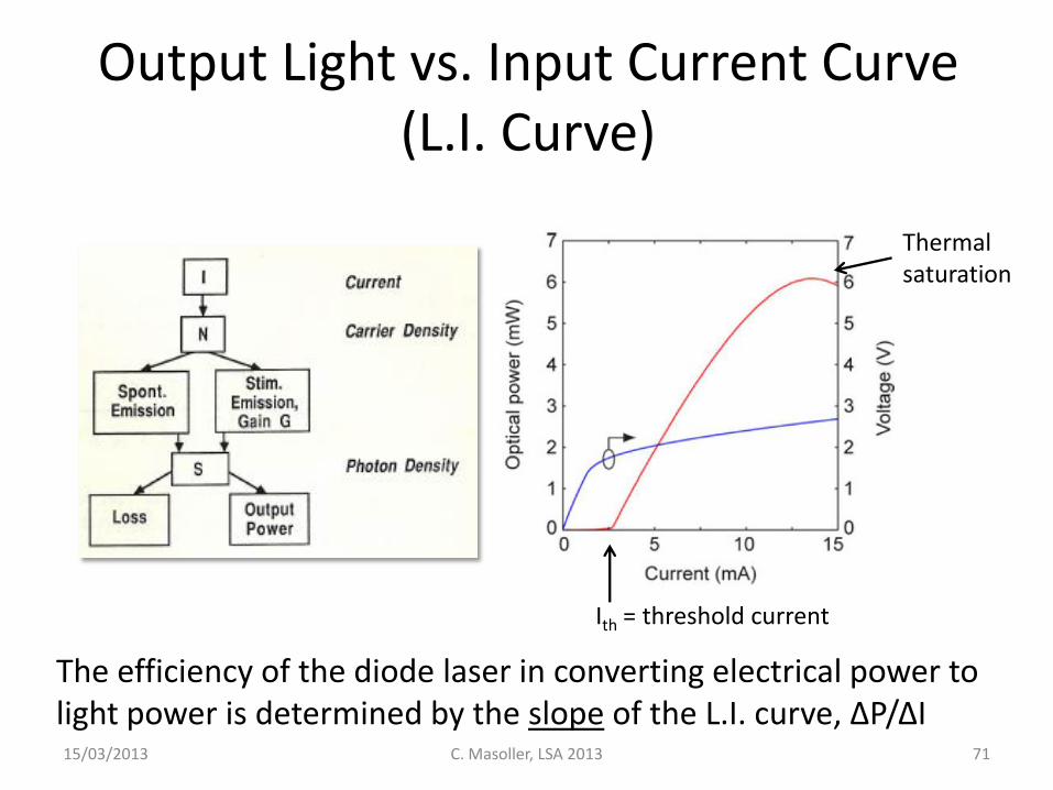
Output Light vs. Input Current Curve (L.I. Curve)
15/03/2013 C. Masoller, LSA 2013 71
Ith = threshold current
The efficiency of the diode laser in converting electrical power to light power is determined by the slope of the L.I. curve, ΔP/ΔI
Thermal saturation
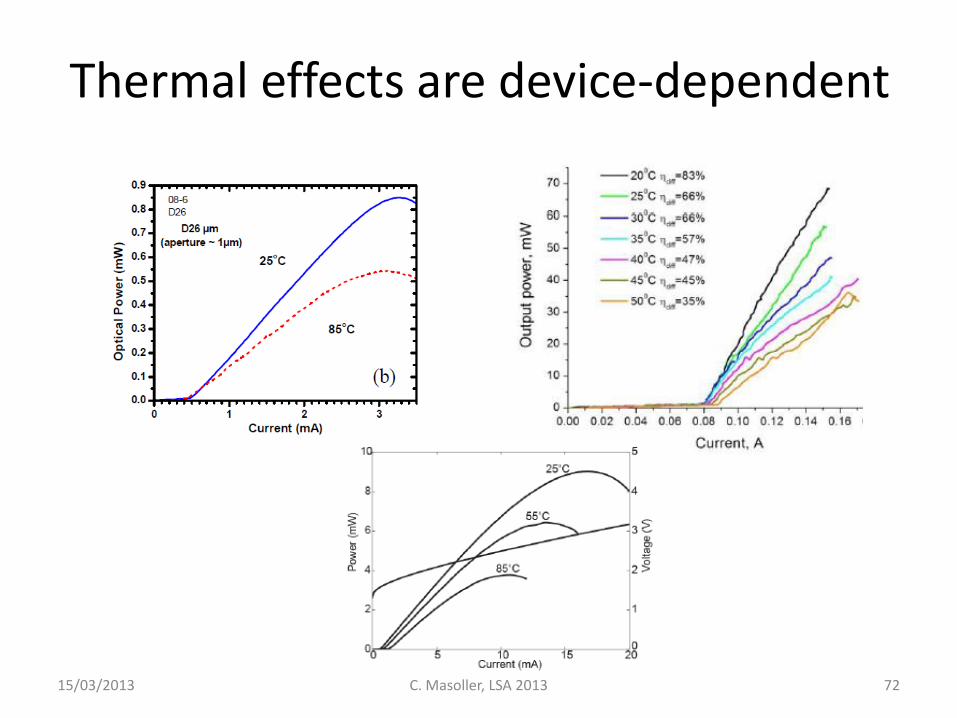
Thermal effects are device-dependent
15/03/2013 C. Masoller, LSA 2013 72
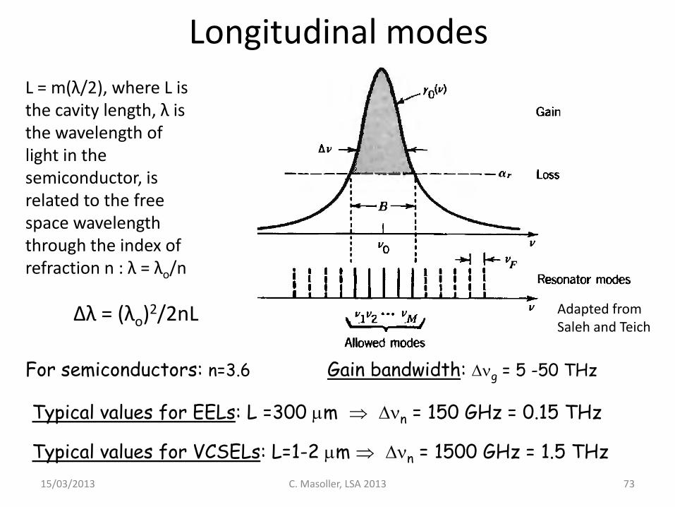
Longitudinal modes
Typical values for EELs: L =300 m n = 150 GHz = 0.15 THz
Typical values for VCSELs: L=1-2 m n = 1500 GHz = 1.5 THz
For semiconductors: n=3.6 Gain bandwidth: g = 5 -50 THz
15/03/2013 73 C. Masoller, LSA 2013
Adapted from Saleh and Teich
L = m(λ/2), where L is the cavity length, λ is the wavelength of light in the semiconductor, is related to the free space wavelength through the index of refraction n : λ = λo/n
Δλ = (λo)2/2nL
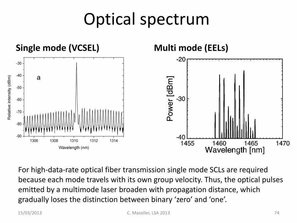
Optical spectrum
Single mode (VCSEL) Multi mode (EELs)
15/03/2013 C. Masoller, LSA 2013 74
For high-data-rate optical fiber transmission single mode SCLs are required because each mode travels with its own group velocity. Thus, the optical pulses emitted by a multimode laser broaden with propagation distance, which gradually loses the distinction between binary ‘zero’ and ‘one’.
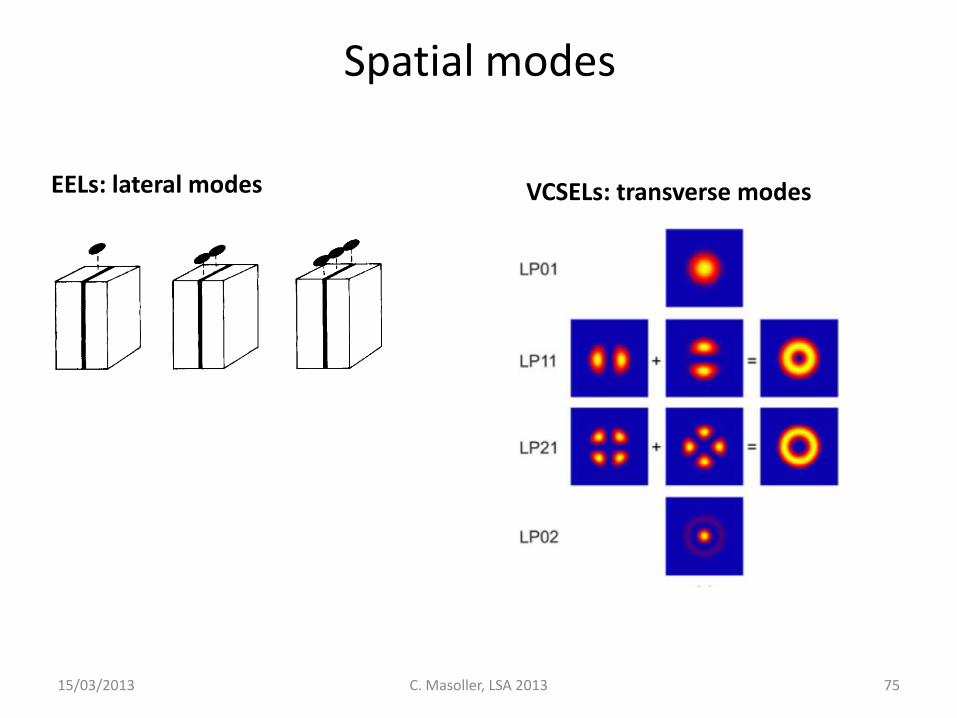
EELs: lateral modes
15/03/2013 75 C. Masoller, LSA 2013
Spatial modes
VCSELs: transverse modes
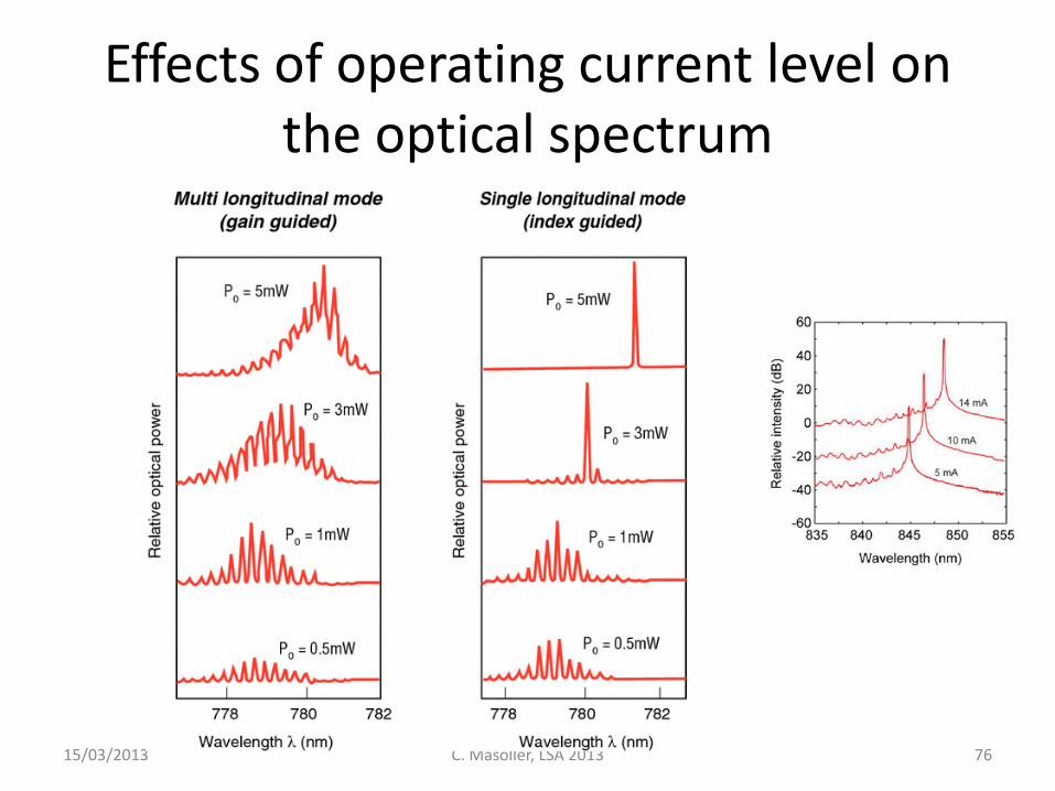
Effects of operating current level on the optical spectrum
15/03/2013 C. Masoller, LSA 2013 76
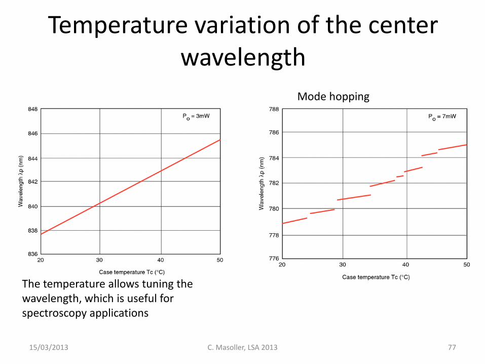
Temperature variation of the center wavelength
15/03/2013 C. Masoller, LSA 2013 77
The temperature allows tuning the wavelength, which is useful for spectroscopy applications
Mode hopping
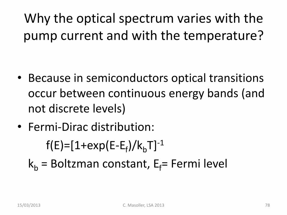
Why the optical spectrum varies with the pump current and with the temperature?
• Because in semiconductors optical transitions occur between continuous energy bands (and not discrete levels)
• Fermi-Dirac distribution:
f(E)=[1+exp(E-Ef)/kbT]-1
kb = Boltzman constant, Ef= Fermi level
15/03/2013 C. Masoller, LSA 2013 78
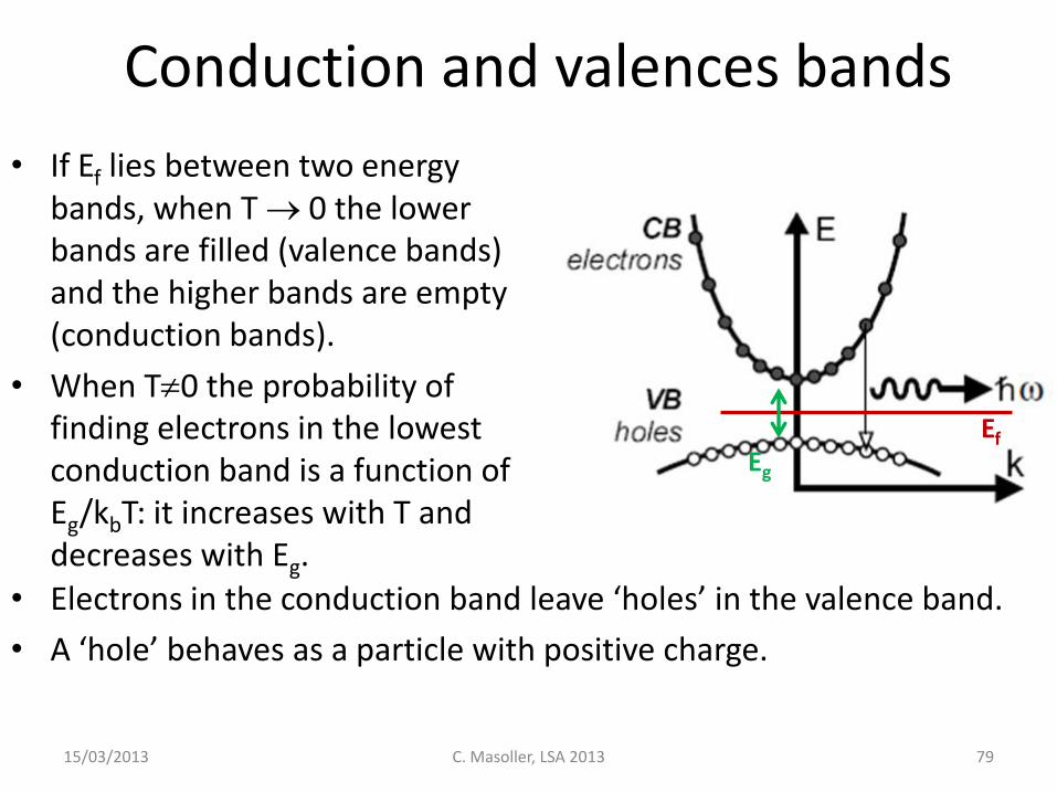
Conduction and valences bands
• If Ef lies between two energy bands, when T 0 the lower bands are filled (valence bands) and the higher bands are empty (conduction bands).
• When T0 the probability of finding electrons in the lowest conduction band is a function of Eg/kbT: it increases with T and decreases with Eg.
15/03/2013 C. Masoller, LSA 2013 79
• Electrons in the conduction band leave ‘holes’ in the valence band.
• A ‘hole’ behaves as a particle with positive charge.
Ef Eg
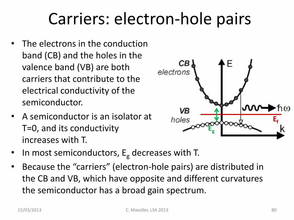
Carriers: electron-hole pairs
15/03/2013 C. Masoller, LSA 2013 80
• The electrons in the conduction band (CB) and the holes in the valence band (VB) are both carriers that contribute to the electrical conductivity of the semiconductor.
• A semiconductor is an isolator at T=0, and its conductivity increases with T.
Ef Eg
• In most semiconductors, Eg decreases with T.
• Because the “carriers” (electron-hole pairs) are distributed in the CB and VB, which have opposite and different curvatures the semiconductor has a broad gain spectrum.
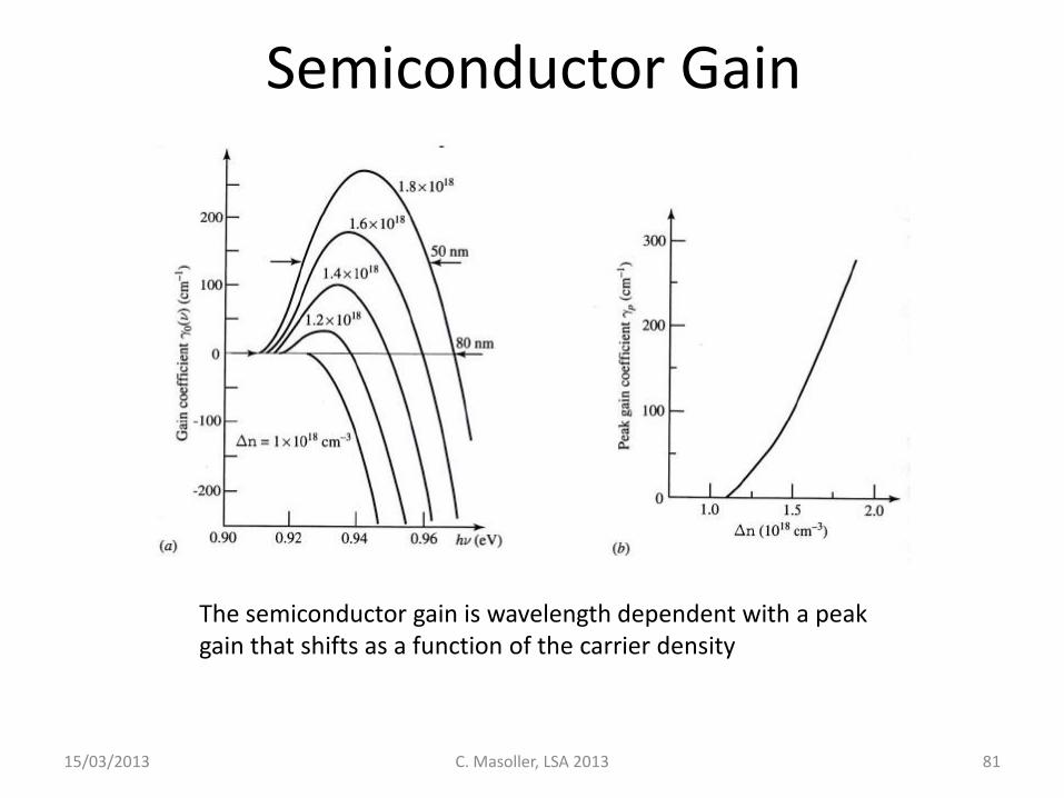
Semiconductor Gain
15/03/2013 C. Masoller, LSA 2013 81
The semiconductor gain is wavelength dependent with a peak gain that shifts as a function of the carrier density
from J. M. Liu, Photonic devices (Cambridge University Press) 15/03/2013 C. Masoller, LSA 2013 82
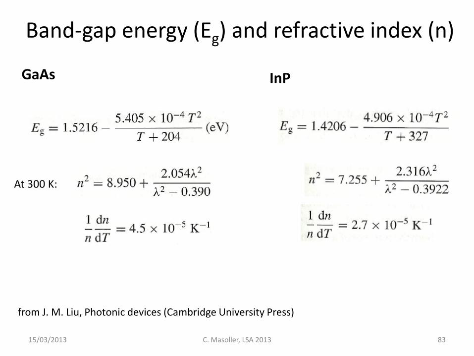
Band-gap energy (Eg) and refractive index (n)
15/03/2013 C. Masoller, LSA 2013 83
GaAs InP
At 300 K:
from J. M. Liu, Photonic devices (Cambridge University Press)
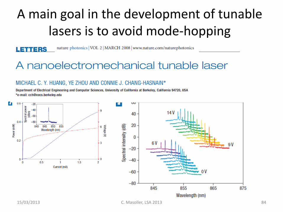
A main goal in the development of tunable lasers is to avoid mode-hopping
15/03/2013 84 C. Masoller, LSA 2013
Electrons and holes concentrations • Concentration: number of electrons in the CB (or holes in the VB) per unit
volume. • Is determined by the type of semiconductor, the temperature and the
external pumping (electrical or optical, injection of electrons or photons) • In an intrinsic semiconductor all electrons in the CB come from thermal
excitation from the VB, electron concentration= hole concentration • In an extrinsic (doped) semiconductor there are impurities: atoms that can
be positively ionized to contribute to a conduction electron (donors) and negatively ionized to contribute a hole to the VB (acceptors).
• In an intrinsic semiconductor the Fermi level is very close to the middle of the band gap
• In an extrinsic semiconductor the Fermi level is a function of the concentration of impurities: – In a n-type (e majority of carriers) is close to the CB – In a p-type (h majority of carriers) is close to the VB
• In thermal equilibrium the concentrations are described by the Fermi-Dirac distribution.
15/03/2013 C. Masoller, LSA 2013 85
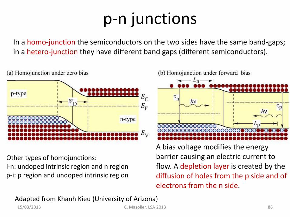
p-n junctions
15/03/2013 C. Masoller, LSA 2013 86
Adapted from Khanh Kieu (University of Arizona)
In a homo-junction the semiconductors on the two sides have the same band-gaps; in a hetero-junction they have different band gaps (different semiconductors).
A bias voltage modifies the energy barrier causing an electric current to flow. A depletion layer is created by the diffusion of holes from the p side and of electrons from the n side.
Other types of homojunctions: i-n: undoped intrinsic region and n region p-i: p region and undoped intrinsic region
Homo-junction vs hetero-junction
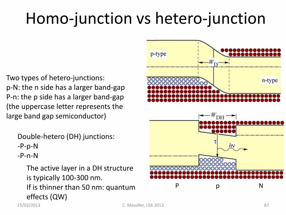
15/03/2013 C. Masoller, LSA 2013 87
Two types of hetero-junctions: p-N: the n side has a larger band-gap P-n: the p side has a larger band-gap (the uppercase letter represents the large band gap semiconductor)
Double-hetero (DH) junctions: -P-p-N -P-n-N
P p N
The active layer in a DH structure is typically 100-300 nm. If is thinner than 50 nm: quantum effects (QW)
Quasi-equilibrium concentrations: relaxation processes
• With current injection or optical excitation electrons and holes in excess of the equilibrium values can be generated.
• The carriers relax towards the equilibrium distribution with – Intraband relaxation processes (1fs-1ps) electron-electron or hole-hole collisions, electron/hole -phonon
interactions – Interband relaxation processes Electron-hole recombination processes (100 ps-1 ms)
• Due to the different time-scales: intraband equilibrium, interband not in equilibrium
• Quasiequilibrium distributions: electrons and holes concentrations are described by two Fermi levels.
15/03/2013 C. Masoller, LSA 2013 88
Electron-hole recombination processes They lead to the annihilation of one electron with one hole • Shockley-Read process: an electron or a hole is captured by an impurity. If
an electron is captured, to conclude the recombination process then a hole has be to ba captured. The recombination process can be either radiative or non-radiative.
• Bimolecular processes: band-to-band recombination and exciton recombination (an exciton is a pair e/h held together by Coulomb attraction, in the same way as the pair e/p forming a hydrogen atom. Radiative processes.
• Auger processes: three particles involved (either 2 e & 1h or 1 e and 2 h). The energy released by band to band recombination of an electron and a hole is picked up by a third carrier, as kinetic energy. Is a nonradiative process.
Carrier recombination rate: R = A n + B n2 + C n3
Carrier lifetime: when the carrier concentration is higher than the equilibrium
value, it will decay with a characteristic time constant, N = (n-n0)/R 1/N A
15/03/2013 C. Masoller, LSA 2013 89
Radiative efficiency, optical transition rates
• R = Rrad + Rnonrad
• Radiative efficiency or internal quantum efficiency: = Rrad/R
• R includes spontaneous electron-hole recombination processes but not the recombination rate due to stimulated recombination.
• The rate of stimulated electron-hole recombination can be calculated from the optical transition rates: absorption, stimulated emission and spontaneous emission
• Ra()d =Re()d +Rsp()d
15/03/2013 C. Masoller, LSA 2013 90

Absorption and gain coefficients
• Ra()d =Re()d +Rsp()d
• ()=h [Ra()-Re()]/I()
• g ()=h [Re()-Ra()]/I() • g ()=- () • Excess carrier density N = n-no = p – po
• High electron and hole concentrations, n>>no, p>>po, lead to a positive optical gain coefficient.
• Transparency carrier density, Ntr: minimum carrier density required for gain.
15/03/2013 C. Masoller, LSA 2013 91
Carrier dependence of the gain
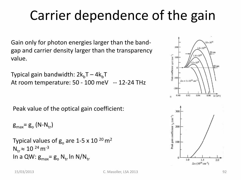
15/03/2013 C. Masoller, LSA 2013 92
Gain only for photon energies larger than the band-gap and carrier density larger than the transparency value. Typical gain bandwidth: 2kbT – 4kbT At room temperature: 50 - 100 meV -- 12-24 THz
Peak value of the optical gain coefficient: gmax= go (N-Ntr) Typical values of go are 1-5 x 10 20 m2
Ntr 10 24 m-3
In a QW: gmax= go Ntr ln N/Ntr
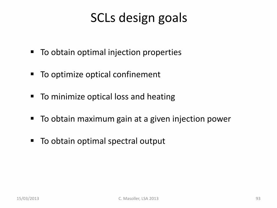
SCLs design goals
To obtain optimal injection properties
To optimize optical confinement
To minimize optical loss and heating
To obtain maximum gain at a given injection power
To obtain optimal spectral output
15/03/2013 93 C. Masoller, LSA 2013
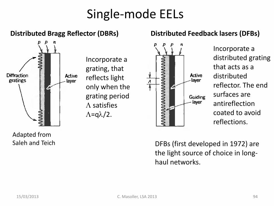
Single-mode EELs
Distributed Bragg Reflector (DBRs) Distributed Feedback lasers (DFBs)
DFBs (first developed in 1972) are the light source of choice in long-haul networks.
Incorporate a grating, that reflects light only when the grating period satisfies =q/2.
Incorporate a distributed grating that acts as a distributed reflector. The end surfaces are antireflection coated to avoid reflections.
Adapted from Saleh and Teich
15/03/2013 94 C. Masoller, LSA 2013
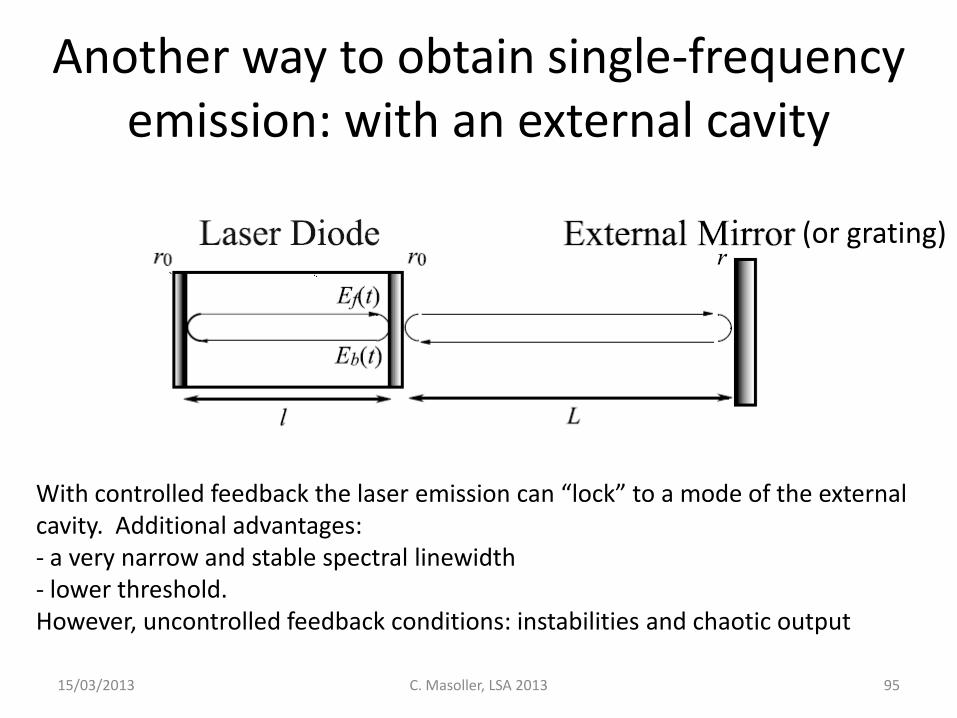
Another way to obtain single-frequency emission: with an external cavity
15/03/2013 C. Masoller, LSA 2013 95
With controlled feedback the laser emission can “lock” to a mode of the external cavity. Additional advantages: - a very narrow and stable spectral linewidth - lower threshold. However, uncontrolled feedback conditions: instabilities and chaotic output
(or grating)
Why the need of narrow stable spectral linewidth?
• The ever-growing demand for increased data rates is pushing optical communications towards coherent communications, whereby information is carried primarily in the phase of the optical wave rather than in its amplitude.
• For example, a single optical pulse that can possess any one of N optical phases can transmit ln2(N) bits per pulse; binary amplitude modulation, can transmit only two bits.
• Achieving phase coherent communications require great phase stability; i.e., a SCL with a narrow spectral linewidth.
• Nowadays DFBs have typical spectral linewidths of 0.5 MHz.
15/03/2013 C. Masoller, LSA 2013 96
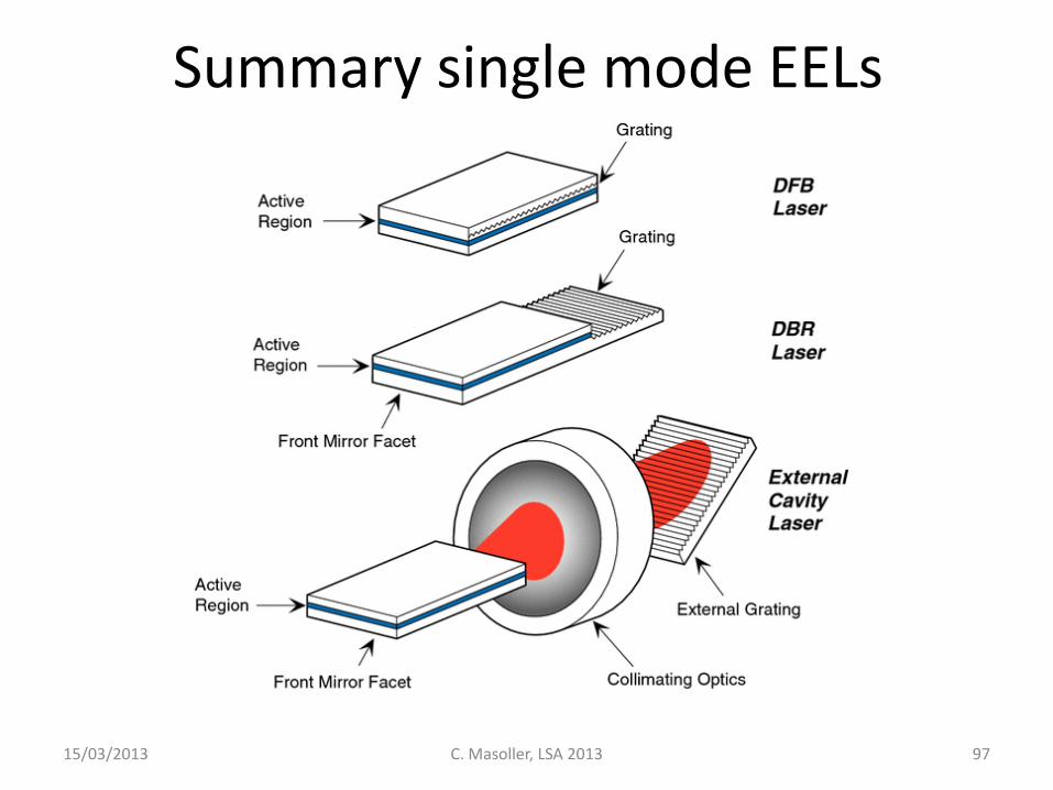
Summary single mode EELs
15/03/2013 C. Masoller, LSA 2013 97
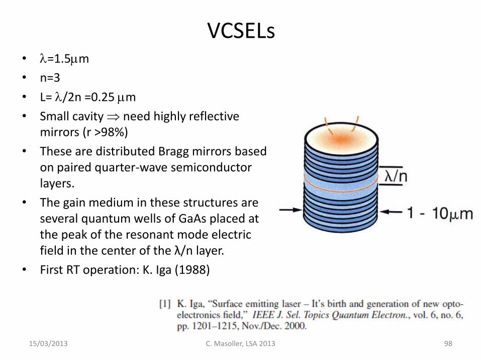
VCSELs • =1.5m
• n=3
• L= /2n =0.25 m
• Small cavity need highly reflective mirrors (r >98%)
• These are distributed Bragg mirrors based on paired quarter-wave semiconductor layers.
• The gain medium in these structures are several quantum wells of GaAs placed at the peak of the resonant mode electric field in the center of the λ/n layer.
• First RT operation: K. Iga (1988)
15/03/2013 98 C. Masoller, LSA 2013
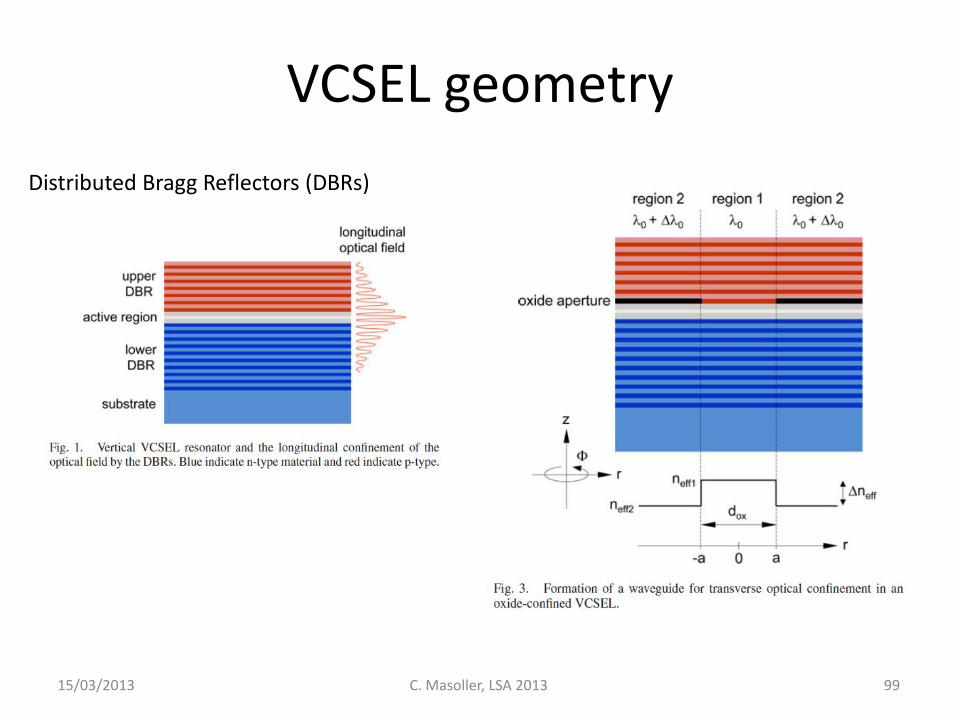
VCSEL geometry
15/03/2013 C. Masoller, LSA 2013 99
Distributed Bragg Reflectors (DBRs)
15/03/2013 C. Masoller, LSA 2013 100
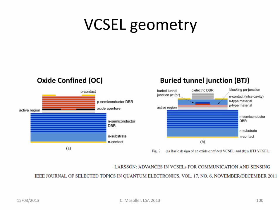
Oxide Confined (OC) Buried tunnel junction (BTJ)
VCSEL geometry
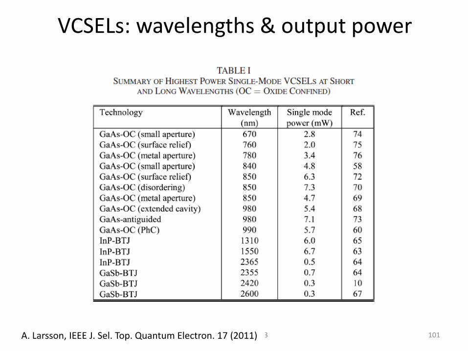
15/03/2013 101 C. Masoller, LSA 2013 A. Larsson, IEEE J. Sel. Top. Quantum Electron. 17 (2011)
VCSELs: wavelengths & output power
4. Dynamic characteristics of SCLs • Relaxation oscillations, modulation bandwidth • Intensity noise, laser linewidth • Optical injection and injection locking • Optical feedback • Light polarization
15/03/2013 C. Masoller, LSA 2013 102
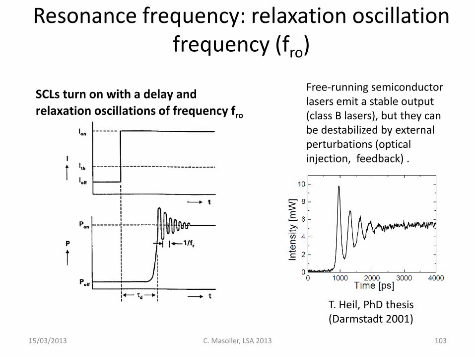
Resonance frequency: relaxation oscillation frequency (fro)
15/03/2013 C. Masoller, LSA 2013 103
T. Heil, PhD thesis (Darmstadt 2001)
SCLs turn on with a delay and
relaxation oscillations of frequency fro
Free-running semiconductor lasers emit a stable output (class B lasers), but they can be destabilized by external perturbations (optical injection, feedback) .
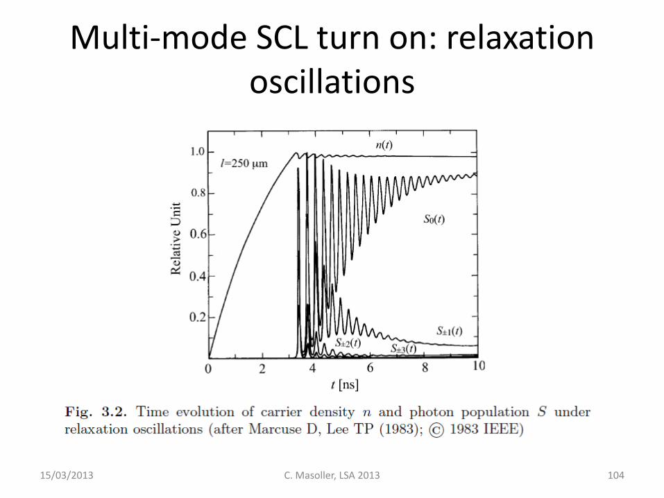
Multi-mode SCL turn on: relaxation oscillations
15/03/2013 C. Masoller, LSA 2013 104
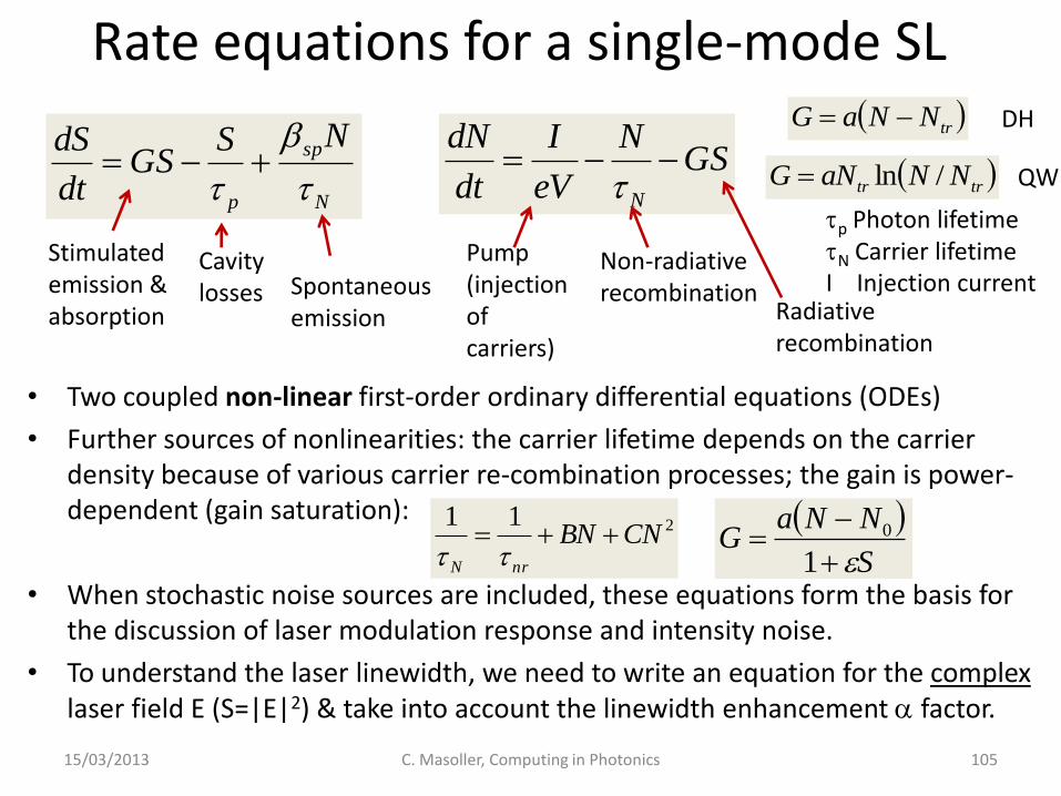
• Two coupled non-linear first-order ordinary differential equations (ODEs)
• Further sources of nonlinearities: the carrier lifetime depends on the carrier density because of various carrier re-combination processes; the gain is power-dependent (gain saturation):
• When stochastic noise sources are included, these equations form the basis for the discussion of laser modulation response and intensity noise.
• To understand the laser linewidth, we need to write an equation for the complex laser field E (S=|E|2) & take into account the linewidth enhancement factor.
15/03/2013 C. Masoller, Computing in Photonics 105
GSN
eV
I
dt
dN
N
N
sp
p
NSGS
dt
dS
trNNaG
S
NNaG
1
0211CNBN
nrN
Rate equations for a single-mode SL
Pump (injection of carriers)
Non-radiative recombination
Radiative recombination
Stimulated emission & absorption
Cavity losses Spontaneous
emission
p Photon lifetime N Carrier lifetime I Injection current
DH
trtr NNaNG /ln QW
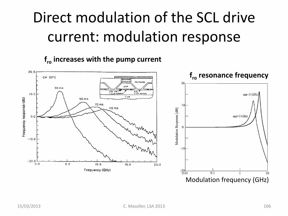
Direct modulation of the SCL drive current: modulation response
15/03/2013 C. Masoller, LSA 2013 106
fro increases with the pump current
Modulation frequency (GHz)
fro resonance frequency
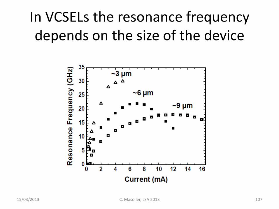
In VCSELs the resonance frequency depends on the size of the device
15/03/2013 C. Masoller, LSA 2013 107
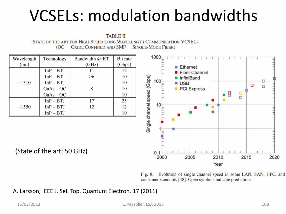
VCSELs: modulation bandwidths
15/03/2013 108 C. Masoller, LSA 2013
A. Larsson, IEEE J. Sel. Top. Quantum Electron. 17 (2011)
(State of the art: 50 GHz)
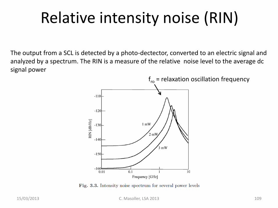
Relative intensity noise (RIN)
15/03/2013 C. Masoller, LSA 2013 109
The output from a SCL is detected by a photo-dectector, converted to an electric signal and analyzed by a spectrum. The RIN is a measure of the relative noise level to the average dc signal power
fro = relaxation oscillation frequency

Laser linewidth and factor • Due to spontaneous emission noise single-mode lasers have a finite
linewidth. • The fundamental limit of the linewidth can be calculated by the
Schawlow and Townes formula, that gives a good approximation for solid-state lasers.
• But in SCL the linewidth is significantly higher than the value predicted by the Schawlow and Townes formula.
• The larger linewidth is due to the intensity and phase noise coupling, caused by a dependence of the refractive index on the carrier density in the semiconductor.
• Henry introduced the linewidth enhancement factor α (also called alpha factor) to quantify this amplitude–phase coupling mechanism.
• The α is an important parameter of SCLs and is a proportionality factor relating phase changes to changes of the gain.
15/03/2013 C. Masoller, LSA 2013 110
Henry, “Theory of the linewidth of semiconductor lasers,” IEEE J. Quantum Electron., vol.QE-18, pp. 259, 1982.
ST 21
4. Dynamic characteristics of SCLs • Relaxation oscillations, modulation bandwidth • Intensity noise and linewidth • Optical injection and injection locking • Optical feedback • Light polarization
15/03/2013 C. Masoller, LSA 2013 111
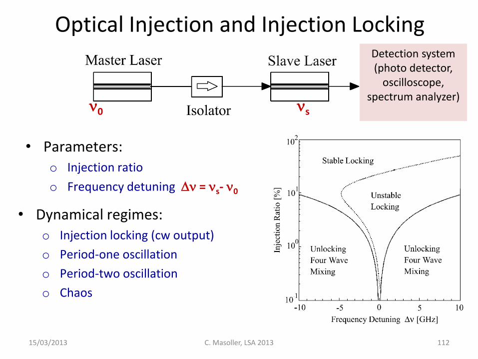
112 C. Masoller, LSA 2013
• Parameters: o Injection ratio
o Frequency detuning = s- 0
• Dynamical regimes: o Injection locking (cw output)
o Period-one oscillation
o Period-two oscillation
o Chaos
0 s
Detection system (photo detector,
oscilloscope, spectrum analyzer)
Optical Injection and Injection Locking
15/03/2013
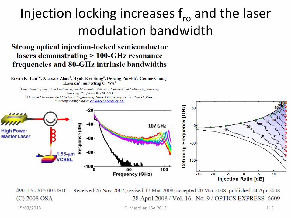
15/03/2013 C. Masoller, LSA 2013 113
Injection locking increases fro and the laser modulation bandwidth
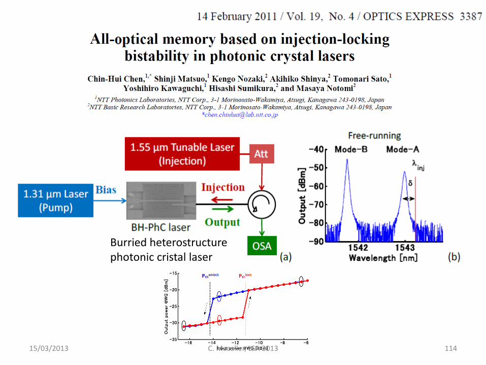
Burried heterostructure photonic cristal laser
15/03/2013 114 C. Masoller, LSA 2013
C. Bonatto et al, PRL 107, 053901 (2011), Optics & Photonics News February 2012
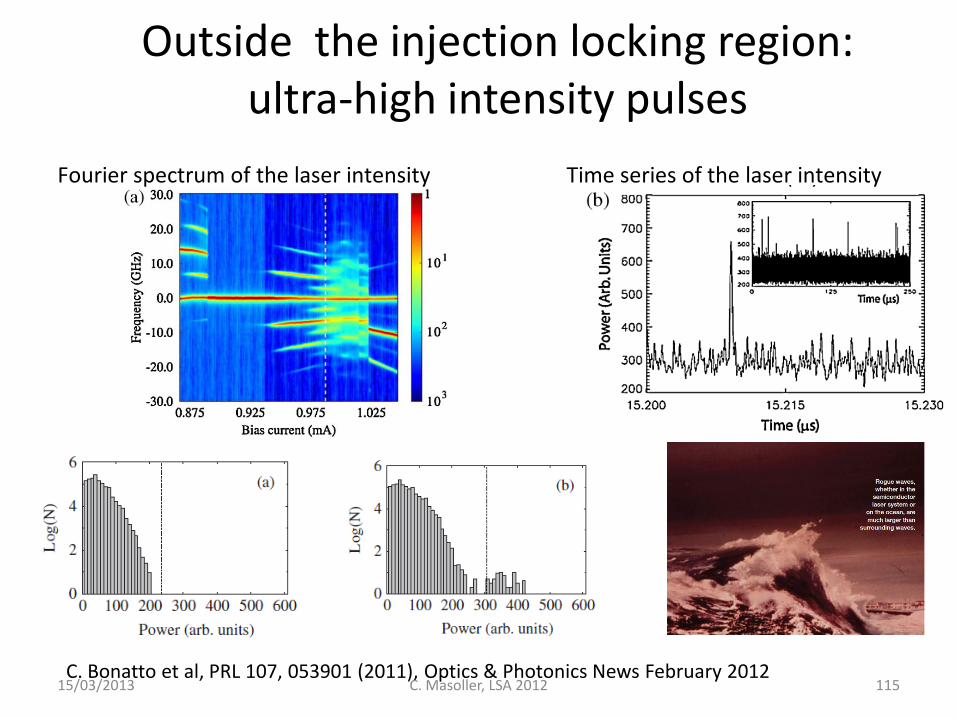
Fourier spectrum of the laser intensity Time series of the laser intensity
15/03/2013 115 C. Masoller, LSA 2012
Outside the injection locking region: ultra-high intensity pulses
4. Dynamic characteristics of SCLs • Relaxation oscillations, modulation bandwidth • Intensity noise and linewidth • Optical injection and injection locking • Optical feedback • Light polarization
15/03/2013 C. Masoller, LSA 2013 116
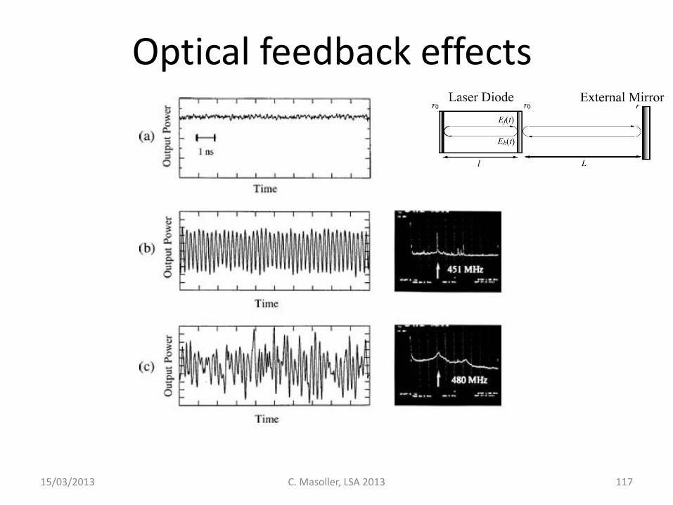
Optical feedback effects
15/03/2013 C. Masoller, LSA 2013 117
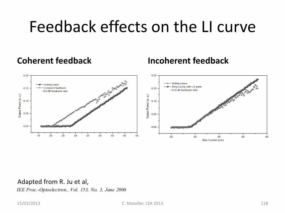
Feedback effects on the LI curve
Coherent feedback Incoherent feedback
15/03/2013 C. Masoller, LSA 2013 118
Adapted from R. Ju et al,
119
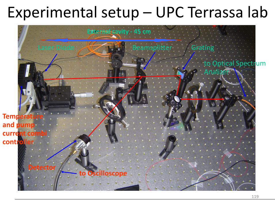
Laser Diode Beamsplitter Grating
Detector to Oscilloscope
Temperature and pump current combi controller
to Optical Spectrum Analizer
External cavity - 45 cm
Experimental setup – UPC Terrassa lab
120
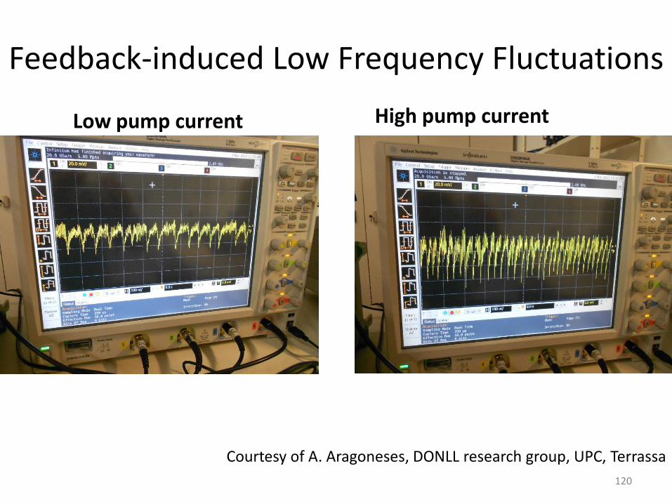
Feedback-induced Low Frequency Fluctuations
Low pump current High pump current
Courtesy of A. Aragoneses, DONLL research group, UPC, Terrassa
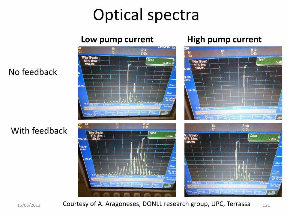
Optical spectra
Low pump current High pump current
15/03/2013 121
No feedback
With feedback
Courtesy of A. Aragoneses, DONLL research group, UPC, Terrassa
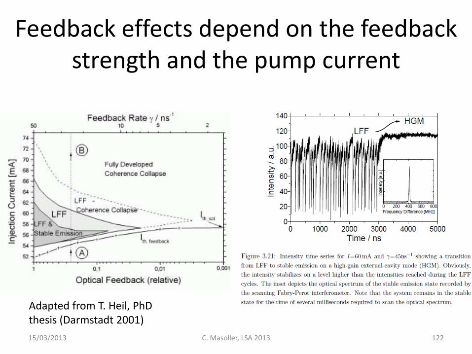
Feedback effects depend on the feedback strength and the pump current
15/03/2013 C. Masoller, LSA 2013 122
Adapted from T. Heil, PhD thesis (Darmstadt 2001)

LFFs: fast pulsing intensity
15/03/2013 C. Masoller, LSA 2013 123
Irregular pulses Regular pulse packages
4. Dynamic characteristics of SCLs • Relaxation oscillations, modulation bandwidth • Intensity noise and linewidth • Optical injection and injection locking • Optical feedback • Light polarization
15/03/2013 C. Masoller, LSA 2013 124
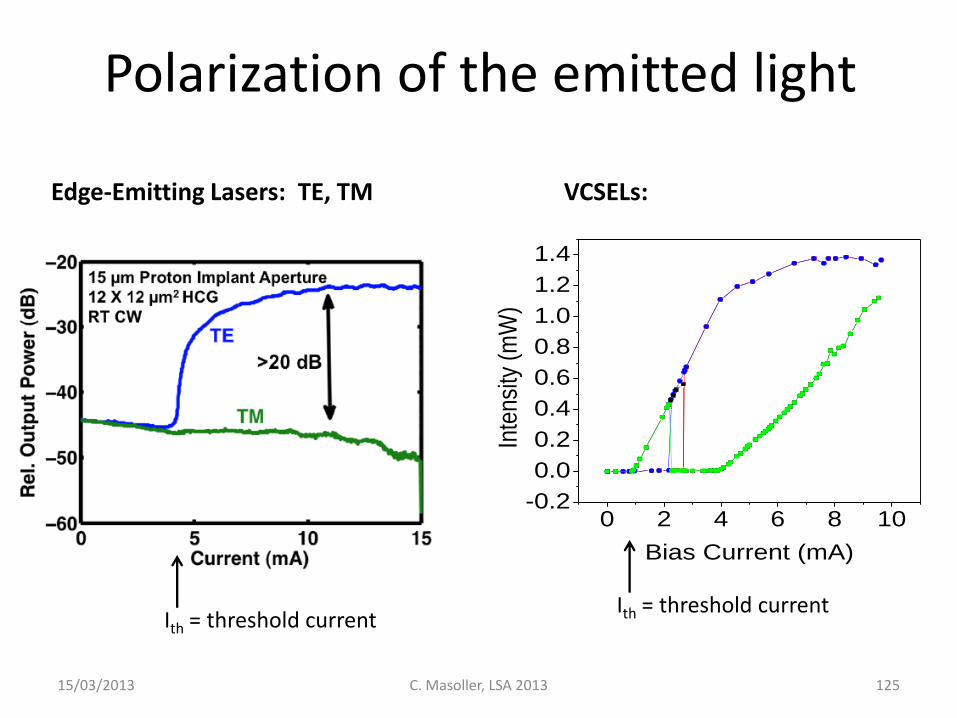
Polarization of the emitted light
0 2 4 6 8 10-0.2
0.0
0.2
0.4
0.6
0.8
1.0
1.2
1.4
Inte
nsity
(m
W)
Bias Current (mA)
Edge-Emitting Lasers: TE, TM VCSELs:
15/03/2013 125 C. Masoller, LSA 2013
Ith = threshold current Ith = threshold current
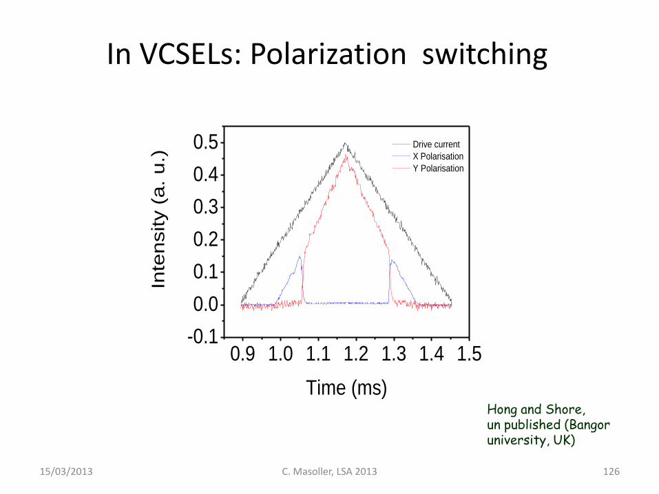
In VCSELs: Polarization switching
0.9 1.0 1.1 1.2 1.3 1.4 1.5-0.1
0.0
0.1
0.2
0.3
0.4
0.5 Drive current
X Polarisation
Y Polarisation
Inte
nsity (
a.
u.)
Time (ms)
15/03/2013 126 C. Masoller, LSA 2013
Hong and Shore, un published (Bangor university, UK)
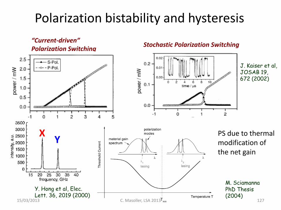
“Current-driven” Polarization Switching
J. Kaiser et al, JOSAB 19, 672 (2002)
Stochastic Polarization Switching
Polarization bistability and hysteresis
PS due to thermal modification of the net gain
M. Sciamanna PhD Thesis (2004)
Y. Hong et al, Elec. Lett. 36, 2019 (2000)
X Y
15/03/2013 127 C. Masoller, LSA 2013
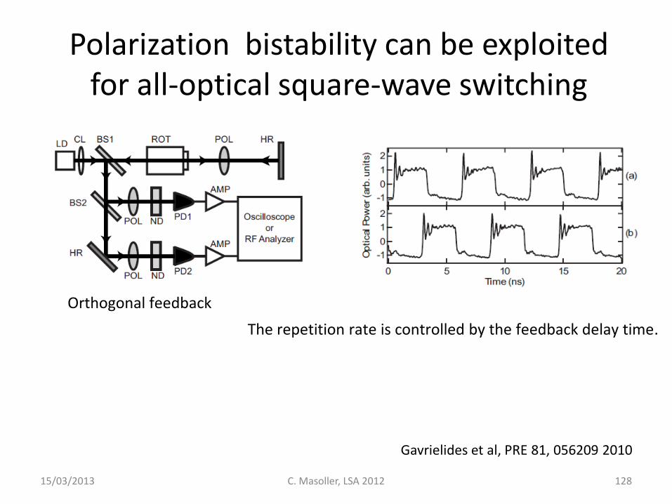
Gavrielides et al, PRE 81, 056209 2010
15/03/2013 128 C. Masoller, LSA 2012
Polarization bistability can be exploited for all-optical square-wave switching
The repetition rate is controlled by the feedback delay time.
Orthogonal feedback
3/15/2013 C. Masoller
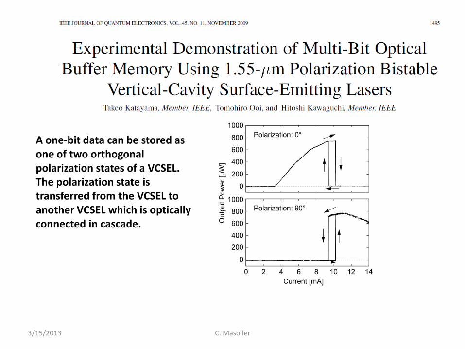
A one-bit data can be stored as one of two orthogonal polarization states of a VCSEL. The polarization state is transferred from the VCSEL to another VCSEL which is optically connected in cascade.
THE NEXT FRONTIERS OF SEMICONDUCTOR LASER RESEARCH
15/03/2013 C. Masoller, LSA 2013 130
Green SCLs • In 1996 the first electrically pumped blue InGaN semiconductor
laser diode was demonstrated (405 nm). • Since then, researchers have found it extremely difficult to push
toward longer wavelengths. Due to the physical and material properties of the InGaN QWs, efficiency drops drastically as diodes move towards green.
• And, unfortunately, this spectral region cannot be reached with other III-V materials, such as AlGaAs orInGaAlP from the long wavelength side.
• In 2009, however, three companies simultaneously demonstrated the first green laser diodes in the range of 515 nm to 530 nm, where the human eye is most sensitive.
• Potential aplications are in biophotonics and the life sciences, such as special microscopy techniques, where laser diodes across the visible spectrum are needed as excitation sources.
• Another application for green laser diodes is expected to be laser-based miniature projectors.
15/03/2013 C. Masoller, LSA 2013 131
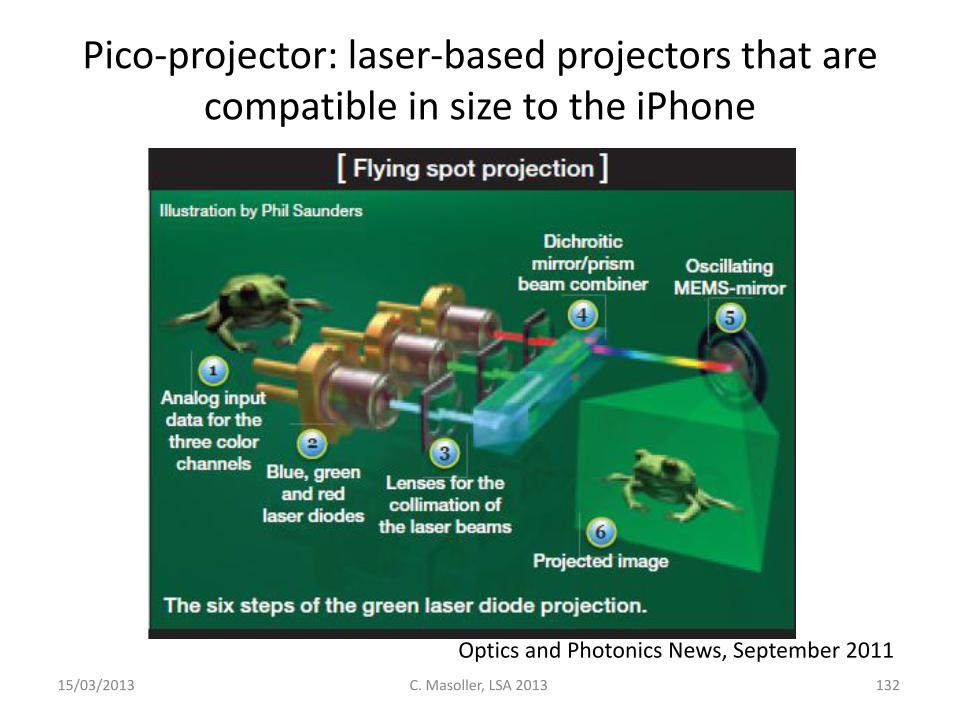
Pico-projector: laser-based projectors that are compatible in size to the iPhone
15/03/2013 C. Masoller, LSA 2013 132
Optics and Photonics News, September 2011
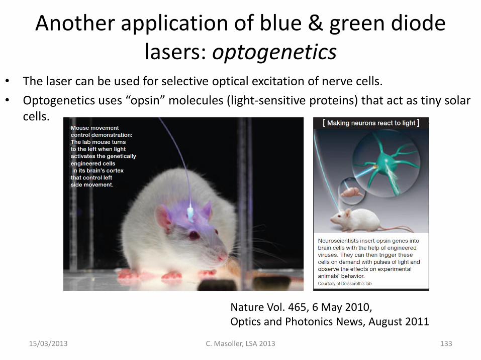
Another application of blue & green diode lasers: optogenetics
• The laser can be used for selective optical excitation of nerve cells.
• Optogenetics uses “opsin” molecules (light-sensitive proteins) that act as tiny solar cells.
15/03/2013 C. Masoller, LSA 2013 133
Nature Vol. 465, 6 May 2010, Optics and Photonics News, August 2011
15/03/2013 C. Masoller, LSA 2013 134
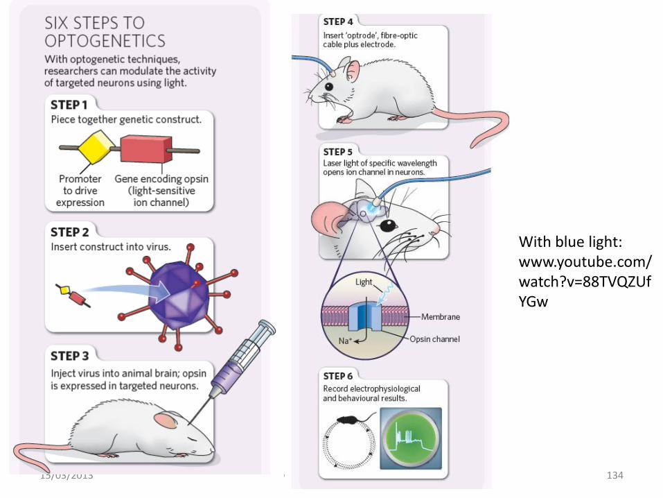
With blue light: www.youtube.com/watch?v=88TVQZUfYGw
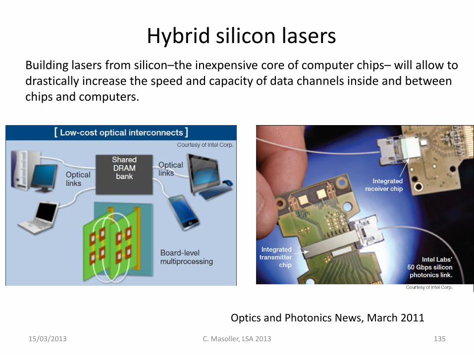
Hybrid silicon lasers
15/03/2013 C. Masoller, LSA 2013 135
Building lasers from silicon–the inexpensive core of computer chips– will allow to drastically increase the speed and capacity of data channels inside and between chips and computers.
Optics and Photonics News, March 2011
15/03/2013 C. Masoller, LSA 2013 136
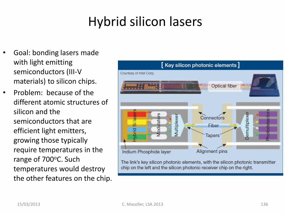
• Goal: bonding lasers made with light emitting semiconductors (III-V materials) to silicon chips.
• Problem: because of the different atomic structures of silicon and the semiconductors that are efficient light emitters, growing those typically require temperatures in the range of 700oC. Such temperatures would destroy the other features on the chip.
Hybrid silicon lasers
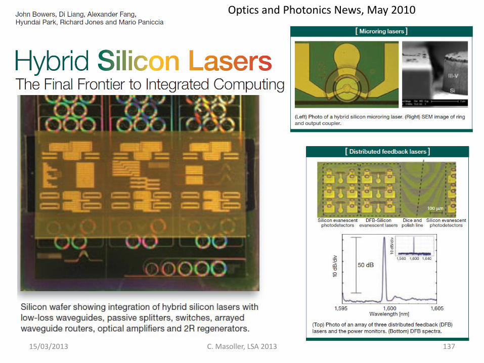
15/03/2013 C. Masoller, LSA 2013 137
Optics and Photonics News, May 2010
15/03/2013 C. Masoller, LSA 2013 138
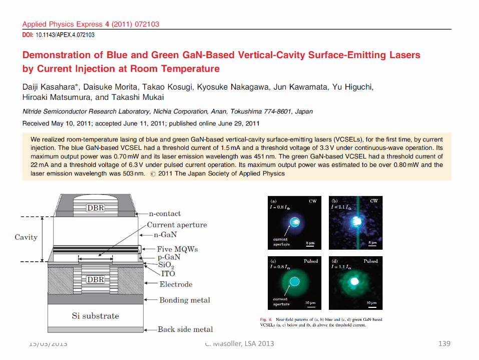
15/03/2013 C. Masoller, LSA 2013 139
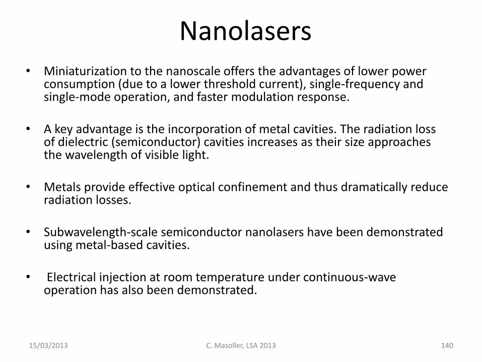
Nanolasers • Miniaturization to the nanoscale offers the advantages of lower power
consumption (due to a lower threshold current), single-frequency and single-mode operation, and faster modulation response.
• A key advantage is the incorporation of metal cavities. The radiation loss of dielectric (semiconductor) cavities increases as their size approaches the wavelength of visible light.
• Metals provide effective optical confinement and thus dramatically reduce radiation losses.
• Subwavelength-scale semiconductor nanolasers have been demonstrated using metal-based cavities.
• Electrical injection at room temperature under continuous-wave operation has also been demonstrated.
15/03/2013 C. Masoller, LSA 2013 140
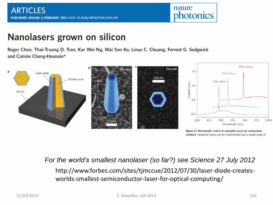
15/03/2013 C. Masoller, LSA 2013 141
For the world’s smallest nanolaser (so far?) see Science 27 July 2012
http://www.forbes.com/sites/tjmccue/2012/07/30/laser-diode-creates-worlds-smallest-semiconductor-laser-for-optical-computing/
15/03/2013 C. Masoller, LSA 2013 142
Recommended literature for further reading
• Saleh and Teich, Fundamentals of photonics – Chapter on Semiconductor injection lasers (16.3)
• J. M. Liu, Photonic devices (Cambridge University Press 2005)
• A. Larsson, Advances in VCSELs for Communication and Sensing, IEEE J. Sel. Top. Quantum Electron. Vol 17, pp 1552, 2011.
• J. Ohtsubo, Semiconductor lasers: stability, instability and chaos (Springer 2008, http://www.springerlink.com)
• Multidimensional optical data storage, Optics and Photonics News, July/August 2010
• Lasers in communications, Optics and Photonics News March 2010
• The green laser diode, Optics and Photonics News September 2011
• Hybrid silicon lasers, Optics and Photonics News May 2010
• Integrated silicon photonics, OPN March 2011
• High-power high-brightness direct-diode lasers, OPN October 2010
15/03/2013 143 C. Masoller, LSA 2012