biofabrication methods for the patterned assembly and
TRANSCRIPT

IOP PUBLISHING NANOTECHNOLOGY
Nanotechnology 21 (2010) 055304 (11pp) doi:10.1088/0957-4484/21/5/055304
Biofabrication methods for the patternedassembly and synthesis of viralnanotemplatesK Gerasopoulos1,2,3, M McCarthy4, P Banerjee2,3, X Fan3,5,J N Culver6 and R Ghodssi1,2,3,5
1 MEMS Sensors and Actuators Laboratory (MSAL), University of Maryland, College Park,MD 20742, USA2 Department of Materials Science and Engineering, University of Maryland, College Park,MD 20742, USA3 Institute for Systems Research, University of Maryland, College Park, MD 20742, USA4 Department of Mechanical Engineering, Massachusetts Institute of Technology,Cambridge, MA 02139, USA5 Department of Electrical and Computer Engineering, University of Maryland, College Park,MD 20742, USA6 Center for Biosystems Research, University of Maryland Biotechnology Institute,MD 20742, USA
E-mail: [email protected]
Received 19 November 2009, in final form 22 November 2009Published 6 January 2010Online at stacks.iop.org/Nano/21/055304
AbstractThis paper reports on novel methodologies for the patterning and templated synthesis ofvirus-structured nanomaterials in two- and three-dimensional microfabricated architecturesusing the Tobacco mosaic virus (TMV). The TMV is a high aspect ratio biological moleculewhich can be engineered to include amino acids with enhanced binding properties. Thesemodifications facilitate self-assembly of the TMV onto various substrates and enable its use as atemplate for the synthesis of nanostructured materials. This work focuses on the combination ofthis bottom-up biologically inspired fabrication method with standard top-downmicromachining processes that allow direct integration of the virus-structured materials intobatch-fabricated devices. Photolithographic patterning of uncoated as well as nickel-coatedTMV nanostructures has been achieved using a lift-off process in both solvent and mild basicsolutions and their assembly onto three-dimensional polymer and silicon microstructures isdemonstrated. In addition to these patterning techniques, in situ formation of metal oxide TMVcoatings in patterned microfabricated environments is shown using atomic layer depositiondirectly on the nickel-coated viruses. The biofabrication ‘process toolbox’ presented in thiswork offers a simple and versatile alternative for the hierarchical patterning and incorporationof biotemplated nanomaterials into micro/nanofabrication schemes.
(Some figures in this article are in colour only in the electronic version)
1. Introduction
A highly desirable requirement for the incorporation ofnanomaterials in practical technological applications ismass production at low cost as well as the abilityto accurately control their properties and arrange themin a highly ordered fashion within a functional device.
Conventional synthesis approaches such as vapor–liquid–solid reactions using catalytic particles, epitaxial methods,electrodeposition, sol–gel and hydrothermal synthesis as wellas patterning techniques based on porous templates, e-beamand conventional lithography often have to balance the trade-off between good control over materials properties, variabilityand compatibility with successive fabrication steps on one hand
0957-4484/10/055304+11$30.00 © 2010 IOP Publishing Ltd Printed in the UK1

Nanotechnology 21 (2010) 055304 K Gerasopoulos et al
and reduced cost on the other [1, 2]. Interestingly, natureoffers unique traits for materials synthesis based on novelfunctionalities that can be imparted on biological structuressuch as proteins, DNA and viruses. Characteristic attributes oftemplating approaches that utilize biological building blocks toguide the assembly of inorganic materials include low cost andstructural versatility of the biologicals, inherent self-assemblyproperties, the existence of functional groups that catalyzeparticle growth and the ability to tune their structure throughgenetic modifications [3].
Among these biological molecules, plant and bacteriaviruses have attracted notable interest for bionanotechnologyapplications. In addition to their self-assembly and tunabilityproperties, they show exceptional stability in a widerange of temperatures and pH values and have even beenreported to withstand treatment in solvent-water mixtures [4].Representative examples of biotemplated viral engineeringhave been achieved with the M-13 bacteriophage viruswhich has been genetically modified through phage displaytechniques to include specific peptides for inorganic materialbinding and nanoparticle fabrication [5]. In this work, we focuson the Tobacco mosaic virus (TMV), a rigid rod consistingof about 2130 identical coat protein subunits stacked in ahelix around a single strand of plus sense RNA, leavinga 4 nm diameter channel through the 300 nm long virionaxis. The TMV in one of the best-studied viruses and hasbeen extensively used in nanowire fabrication [6]. Previouswork by our team has utilized engineered mutations of theTMV to improve coating uniformity of nano-sized particles;more specifically, efficient templates have been achievedthrough the introduction of one (TMV1cys) or two (TMV2cys)cysteine residues within the virus coat protein open readingframe. Cysteines are amino acids with thiol groups that showenhanced metal binding properties based on strong, covalent-like interactions. Using this methodology, TMV-based wirescoated with gold, silver, palladium, platinum, cobalt, nickelas well as multilayer structures of metal–silica–metal particleshave been synthesized and shown to self-assemble in avertical orientation onto gold surfaces [7]. The feasibility ofusing these coated nanostructures in functional microfabricateddevices has been previously demonstrated through thedevelopment of a TMV-based nickel–zinc microbattery [8].
While considerable progress has been achieved in thesynthesis of nanomaterials based on biological templates,their integration into high-throughput manufacturing processesis still a concern. Reported approaches include scanningprobe and dip-pen nanolithography techniques that utilizecantilever tips to transfer molecules of interest to a substratethrough capillary and chemical interactions [9]. Salaita et aldemonstrated a novel variation of this technique where 55 000such tips can be used for parallel patterning thus addressingthe time limitation needed for processing [10]. Selectiveplacement of DNA nanowires has been achieved through self-assembly and functionalization with chemical groups as wellas DNA hybridization [11]; this approach has been previouslyutilized by our group to selectively assemble fluorescently-tagged TMV onto a chitosan-functionalized electrode [12].An alternative method was presented by Kuncicky et al who
demonstrated long-range alignment of TMV conductive fibersby dragging a meniscus of virus suspension on substrates withcontrolled wettability [13]. Viruses and proteins have also beenarranged on substrates through micro-contact printing [14].This technique uses an elastomeric structure fabricated throughsoft-lithography which is then wetted with the functionalmaterial and stamped on the target substrate. Alternatively,the stamping process has been used to selectively patternpolyelectrolyte multilayers on which viruses can successivelyassemble [15]. Notwithstanding individual advantages of thesemethods, they often require special surface treatment (eitherthe target substrate or intermediate layer) which makes themsensitive to processing conditions; they cannot always bescaled up at the wafer level or show compatibility with batchfabrication, attributes very important for large-scale productionand device integration.
The work presented in this paper describes a simpleand versatile approach for the selective patterning of bothmetal-coated and uncoated TMV using a lift-off process.The technique requires a single photolithography step andis readily achieved at the wafer level. Additionally, unlikemost reported methodologies, the TMV self-assembly andpatterning is also performed onto complex out-of-planemicrofabricated geometries. Finally, the robustness of thecoated TMV is utilized for the in situ synthesis of high surfacearea vertically-assembled core/shell TMV–nickel/metal oxidenanomaterials using an atomic layer deposition (ALD) coatingstep, thus expanding the toolbox of available chemistries thatcan be combined with the viral template. The patterningmethodologies and structures presented in this paper arecurrently integrated by our team in projects that utilize theTMV template as a building block. These include selectivepatterning of virus receptor layers for gas sensing applications,structuring and patterning of nanostructured Li-ion batteryelectrodes, and development of hierarchical structures forsuperhydrophobic and superhydrophilic surfaces; results fromthese investigations will be the focus of future publications.
2. Experimental methods
2.1. Materials
Silicon wafers (p-type, 4 inch, 〈100〉 test grade) werepurchased from Silicon Quest Int. (NV, USA). PhotoresistsShipley 1813 and SU-8 50 and developers Microposit 352and SU-8 developer were purchased from Microchem (MA,USA). Photoresists AZ5214 and AZ9245 and developerAZ400K were purchased from MaysChem (IN, USA). Sodiumtetrachloropalladate (NaPdCl4, 98%), nickel (II) chloridehexahydrate (NiCl2, 99%), sodium tetraborate (Na2Ba4O7,99%), dimethylamine borane (DMAB, 97%), were purchasedfrom Sigma Aldrich (MO, USA). Glycine (tissue Grade) waspurchased from Fischer Scientific (PA, USA). 10 ml of 10 mMPd catalyst solution was prepared by dissolving 29.419 mgof NaPdCl4 in de-ionized (DI) water. Nickel plating solution(25 ml) was prepared by mixing 0.6 g NiCl2, 0.45 g Glycine,1.5 g Na2B4O7, 0.77 g DMAB and DI water and stirringuntil the pH of the solution becomes 7. TMV1cys was
2

Nanotechnology 21 (2010) 055304 K Gerasopoulos et al
Figure 1. Schematic representation of the lift-off patterning processes for nickel-coated TMV (a), uncoated TMV (b) and uncoated TMV withan etched recess—(a). Coated TMV: e-beam evaporation of Ti/Au (i), photolithography with positive or negative photoresist (ii), TMVassembly and Ni coating (iii) and removal of photoresist in acetone (iv). (b) Uncoated TMV: photolithography with positive photoresist (i),Ti/Au evaporation (ii), TMV assembly (iii), lift-off of Au and TMV in a developer mixture or acetone (iv). (c) Uncoated TMV. Afterphotolithography, a shallow recess (1 µm) is etched using DRIE (i), steps (ii)–(iv) are identical.
prepared purified according to standard previously reportedmethodologies [16, 17].
2.2. TMV patterning
The basic concept of the TMV photolithographic patterning isderived from the conventional lift-off process that is used inthe MEMS and semiconductor industry to pattern metallizationlines. Photoresist is used to transfer the desired features froman optical mask onto the wafer which is then immersed intoa pH 7 phosphate buffer (PBS) solution containing the virus.After TMV self-assembly on the substrate, the photoresist isremoved in a solvent or developer solution, leaving TMV onlyon the patterned surfaces. Depending on the type of TMVnanostructure that has to be patterned (uncoated TMV1cys ornickel-coated TMV1cys), this general approach is modifiedaccordingly to facilitate processing as well as characterizationof the samples using high resolution microscopy techniques.Both methodologies are shown schematically in figure 1 anddescribed in detail in the following subsections.
2.2.1. Nickel-coated TMV patterning. The fabrication beginswith evaporation of titanium and gold metal layers on a p-type 4 inch silicon wafer to thicknesses of 10 and 50 nmrespectively. This step is followed by photolithography usingan optical mask that contains various features (lines, squaresand circles) with size and spacing ranging from 100 µm downto 2 µm; this is the minimum feature size that can be obtainedfrom the mask manufacturer for contact alignment. Bothpositive and negative photoresists (Shipley 1813 and image-reversed AZ5214 respectively) with varying thicknesses wereemployed. For Shipley 1813, the wafer was exposed in acontact aligner (Quintel Q-4000) with a dose of 180 mJ cm−2
and developed for 30 s in Microposit 352. When AZ514 was
used, the wafer was exposed with the mask at 40 mJ cm−2,post-exposure baked at 125 ◦C for 45 s and then flood-exposed(no-mask) at 2000 mJ cm−2 to invert the polarity. Developmentwas performed in a mixture of AZ400K developer and waterin a 1:6 ratio for 2 min. After development, the three-stepviral self-assembly and nickel coating process is performedon cleaved chips as previously described [8]. The chips areplaced in a TMV-containing sodium phosphate buffer solutionat a virus concentration of 0.1 mg ml−1 and allowed to incubateovernight. After TMV self-assembly, the die are immersed fora few hours in a palladium catalyst solution prepared by mixinga palladium salt (sodium tetrachloropalladate) with PBS (ratioof 1:10 to 1:15) and finally they are coated with nickel in anelectroless plating solution in which they are immersed for 3–5 min. The metallization step is followed by treatment of thesamples in an acetone bath using ultrasonication.
2.2.2. Uncoated TMV patterning. The process begins withthe photolithography step using Shipley 1813 as the positiveresist on a 4 inch silicon wafer with the same optical mask.The photoresist is exposed for 15 s under UV light andthen developed with Microposit 352. After development,the wafer is flood-exposed for 30–40 s to allow lift-off inthe developer solution. Before metallization, some of thewafers are shallow-etched with Deep Reactive Ion Etching(DRIE) to a depth of approximately 1 µm (figure 1(c)); thissmall fabricated recess was expected to accelerate the lift-offprocess and was investigated for comparison with the standardmethod. E-beam evaporation is then used to deposit thin filmsof titanium (10 nm) and gold (50 nm) on the wafer. Finally,the wafer is cleaved and the individual chips are immersed inthe TMV-containing solution (concentration of ∼0.1 mg ml−1)and allowed to incubate overnight.
3

Nanotechnology 21 (2010) 055304 K Gerasopoulos et al
Figure 2. SEM images of patterned nickel-coated TMV features; (a) microfabricated virus-coated lines with size and spacing of 2 µm and(b) close-up view of the textured surface.
2.3. Three-dimensional microstructure fabrication
Silicon structures were etched in the STS with a rate of3 µm min−1 to a depth of 240 µm. The etching mask wasa 5.5 µm thick AZ9245 photoresist. The resist was spun atspeeds of 1750 rpm for 5 s and 3000 rpm for 40 s and soft-baked at 110 ◦C for 90 s. The wafer was exposed at a dose of300 mJ cm−2 and developed in a mixture of AZ400K and DIwater in a 1:3 ratio. After etching, photoresist was removedin acetone and layers of chrome (50 nm) and gold (250 nm)were sputtered on the substrate in an AJA sputtering unit. Thepolymer structures were fabricated on silicon wafers whichwere cleaned in acetone, methanol, isopropyl alcohol and DIwater in ultrasonics and dehydrated at 200 ◦C for 20 min.SU-8 50 was spun at speeds of 600 rpm and 2500 rpm and soft-baked at 75 ◦C with a ramp of 300 ◦C h−1 for 50 min. Exposurewas performed in the aligner for 80 s and post-exposure bakefollowed under the same conditions as the soft-bake. Thewafer was finally developed in SU-8 developer for 10 min withagitation.
2.4. Synthesis of core/shell nickel/metal oxide nanostructuresusing ALD
The nickel-coated patterned chips were placed in a TFS500 BENEQ™ ALD reactor. The deposition of Al2O3
was performed using alternate pulse sequences of trimethylaluminum (TMA) and H2O at 220 ◦C while the depositionof TiO2 utilized tetrakis-dimethyl amido titanium (TDMAT)and H2O at 150 ◦C. The measured deposition rate for theserecipes has been determined to be 0.1 nm/cycle for Al2O3
and 0.05 nm/cycle for TiO2, close to reported values inliterature [18]. The target thickness for both the depositedlayers was kept to be 30 nm to enable observation of a notablechange with the electron microscopy imaging techniques.
2.5. Characterization
SEM images were obtained using a Hitachi SU-70 AnalyticalUHR FEG-SEM. AFM analysis was done using a DigitalInstruments DI-300 atomic force microscope in tapping mode.TEM analysis was done with a JEOL JEM 2100 TEM whileEDS was performed with an Oxford INCA 250 system attachedto a JEOL JEM 2100F TEM/STEM. The TEM sampleswere prepared as follows: chips for TEM analysis were
prepared on a freshly-cleaved mica substrate where a thinlayer of gold has been thermally evaporated to serve as a basefor TMV assembly. The ALD-TMV-coated mica substrateswere first dehydrated in 70%, 95% and 100% (2 times)acetone for 10 min each time. Spurr’s resin was prepared assuggested in [19] and the chips were immersed in mixtures ofacetone:Spurr’s at ratios of 1:1, 1:2 and 1:3 for 30 min eachtime. After immersion in 100% Spurr’s for 1 h, the chip wasembedded in Spurr’s and the resin was polymerized overnightat 70 ◦C in an oven. Thin sections (70 nm) were obtained with adiamond knife and mounted onto carbon/formvar coated TEMgrids.
3. Results and discussion
3.1. Nickel-coated TMV
The patterning approach for the TMV-templated metallicnanostructures is simple and straightforward due to theremarkable robustness of coated viruses in solvents as well asthe ability to characterize the samples directly using scanningelectron microscopy (SEM). Immersion of the photoresist-patterned nickel-coated chips in an acetone bath followed byultrasonication results in lift-off of the underlying photoresistlayer leaving the nickel-coated viruses onto the patternedsurfaces. Figure 2 shows SEM images of the minimumpatterned feature size including a close-up view of the texturedsurface. The SEM images demonstrate that nickel-coatedTMV-structured lines with size and spacing as small as 2 µmcan be clearly resolved. It is also observed that the metalcoating enables nanoscale three-dimensional assembly of theotherwise flat-laying virus resulting in very high surface areapatterns. This near-vertical assembly has been explained indetail in previous publications [7, 8] and it is very important inapplications such as battery electrodes and fuel cell catalystswhere maximum surface area is desirable. The patterningmethodology investigated using this lift-off technique isindependent of the photoresist polarity or thickness and itis limited only by the minimum mask feature size. Whilethe concept has been demonstrated using nickel coating, theprocess has also been successfully combined with other similarsolution-based coating recipes that were developed by ourgroup. This versatility and simplicity make it a very promisingcandidate for large-scale manufacturing of nanostructuredtemplates.
4

Nanotechnology 21 (2010) 055304 K Gerasopoulos et al
3.2. Uncoated TMV
Two important considerations had to be taken into accountwhen developing the fabrication process for the uncoatedTMV. First of all, extensive treatment of the virus in solvents(commonly used solutions for photoresist removal) can resultin structural destabilization of the TMV or other peptides thatcould be potentially attached on the virion surface; this led tothe investigation of alternative methods to remove the polymermasking layer based on less reactive solutions. The secondrequirement is pertinent to the sample characterization whichis conducted with both SEM and atomic force microscopy(AFM) in this experiment so that nanoscale structural effectscan be analyzed. Uncoated TMV cannot be viewed with anoptical microscope and this necessitates the use of ‘alignmentmarks’ to achieve correct placement of the AFM tip onpatterned and unpatterned areas. The first concern is addressedby employing positive photoresist during photolithography,since this type can be treated with UV light after fabricationand removed with both solvent and developer mixtures. Tofacilitate imaging, the base gold layer for TMV assembly isdeposited after photoresist patterning (as in standard lift-off) sothat discrimination between patterned structures can be madeeasily.
Two lift-off methodologies utilizing photoresist developerand an acetone solution were investigated. The developeris a highly basic solution (pH 13–14) consisting of sodiumhydroxide, sodium tetraborate, boric acid and water; forthis application, it was mixed with sodium phosphate buffer(0.1 M, pH 7) at ratios of 1:3 and 1:5 which resulted ina decrease in the pH of the mixture to values of ∼9 and∼8 respectively. These milder conditions were necessary toavoid destabilization of the virus structure. The chips wereimmersed in the solution and placed on a hotplate heatedat 55 ◦C to accelerate the photoresist removal process. Thistemperature was selected again based on literature findingsregarding the virus stability in certain temperature ranges [8].Lift-off in acetone was more straightforward and involvedimmersion of the die in the solvent at room temperature. Inboth cases, slight manual agitation was applied periodicallyto assist the process. The developer-based process was, asexpected, slower and required 5–7 h for patterning of featuresdown to 10 µm. Smaller features required treatment up to 30 hto be completely resolved and partial structural destabilizationwas observed for such long process times. In all cases,continuous agitation accelerated the lift-off rate. On the otherhand, gold/virus lift-off in acetone proceeded at a faster pace(1–2 h for similar feature sizes). It was also observed thatin the wafers without the shallow-etched trenches photoresistremoval was even slower. After completion of the process,the samples were rinsed in DI water and dried on a hotplateat 40 ◦C.
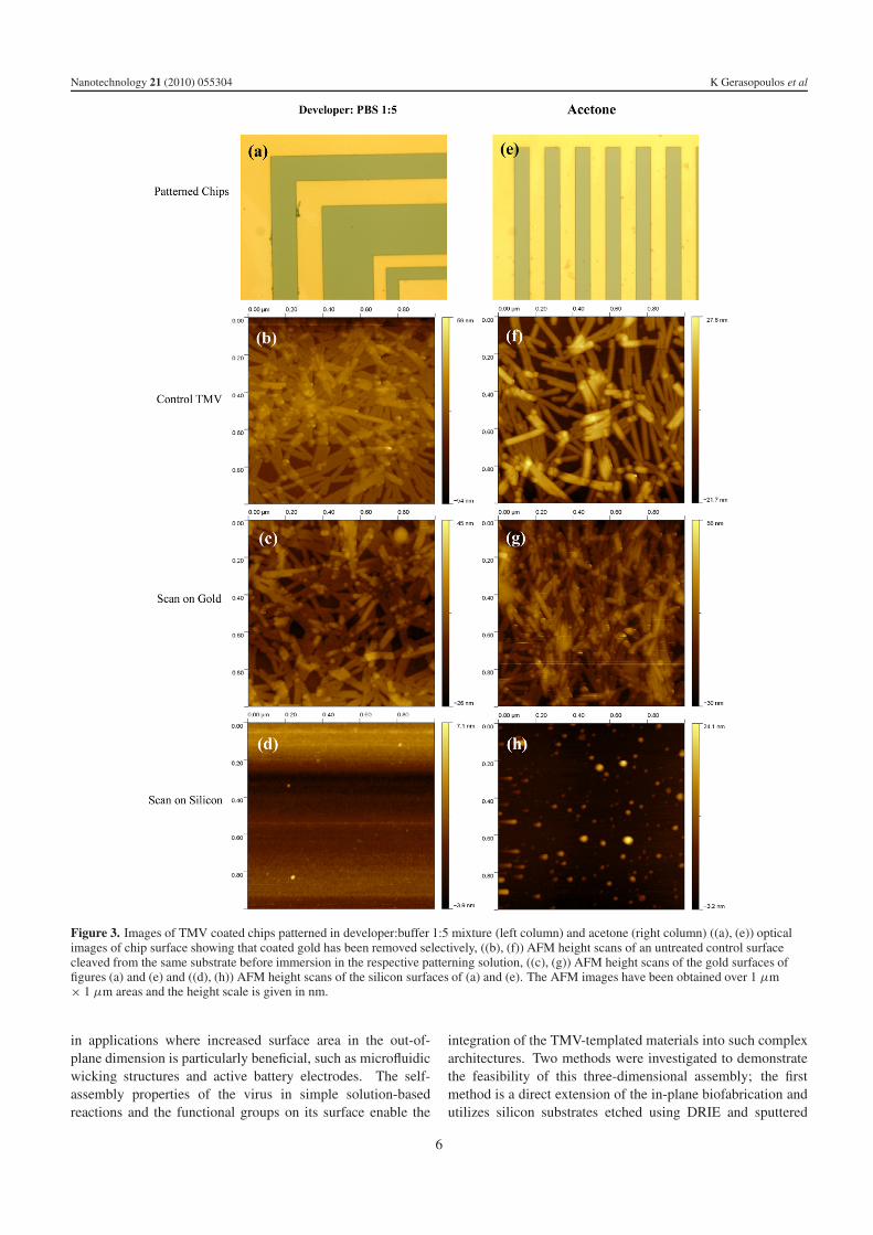
Figures 3(a) and (e) show optical images of chipspatterned in the developer mixture (1:5) and acetonerespectively. It can be clearly seen that gold features havebeen lifted off from the silicon substrate. The nanostructureof the patterned surfaces was investigated using an atomicforce microscope. Figures 3(b) and (f) show height scans ofuntreated TMV surfaces on gold substrates which were used
as control while figures 3(c), (g), (d) and (h) are scans ofgold and silicon areas from the samples of figures 3(a) and (e)respectively. In all images it is seen that, unlike the case ofthe metal-coated TMV, the viruses lay flat on the substrateas a result of the drying process since there is no coatinglayer to provide the three-dimensional support. The interfacebetween the gold and silicon surfaces on chips patterned usingdeveloper mixed with PBS in a 1:3 ratio and acetone areshown in figure 4 where the selectivity in TMV patterningis clearly demonstrated. By comparing the untreated anddeveloper-patterned surfaces it can be observed that the mild-pH lift-off process does not affect the virus structure when thedilution is performed in the range of 1:3 to 1:5. On the otherhand, samples treated in the solvent solution show a differentmorphology compared to the untreated TMV as evident fromthe height scan in both the gold and silicon areas as well as theheight and phase images of figure 4 that show additional virusfragments on the surface. This is attributed to precipitationof the coat proteins in acetone which results in unfolding aswell as fracturing of the virus particles and successive irregularassembly across the chip area.
The post-patterning chemical functionality of the uncoatedTMV was investigated for both techniques by attemptingmetallization of the structures. Optical microscope inspectionwas employed to determine that the gold areas were removedfrom the silicon substrate. Once successful photoresist removalwas verified, the samples were gently rinsed in a PBS solutionwithout prior drying and then metallized with nickel using thetwo-step process described earlier. Figures 5(a) and (b) showcharacteristic SEM images of chips patterned in developer(5:1) and acetone respectively. It is observed in both casesthat the TMV is successfully metallized. In the developer-processed specimens a small number of fragments were foundin the silicon areas, which could be due to re-depositionof solution-excess viruses during the lengthy process. Thiseffect is more pronounced however when TMV is immersedin acetone as was indicated in the AFM analysis as well. Inaddition to cases of TMV fragments, poor coverage of thesubstrates was occasionally observed in acetone.
In conclusion, two lift-off methodologies for thepatterning of uncoated TMV on microfabricated structureshave been successfully developed. The developer-basedprocess is lengthy as several hours are required to resolvevirus-coated structures as small as 10 µm however nostructural degradation or difference in morphology comparedto untreated surfaces has been observed during these times.When the process is performed in acetone, features are liftedoff faster but negative effects on the virus structure have beennoticed with variability even on the same substrate. Since post-patterning chemical functionality is maintained, depending onthe requirements of a specific process, the most suitable of thetwo techniques can be adopted.
3.3. Assembly of coated TMV on three-dimensionalgeometries
Assembly of high aspect ratio nanostructures on three-dimensional microstructures is a very attractive approach
5
Nanotechnology 21 (2010) 055304 K Gerasopoulos et al
Figure 3. Images of TMV coated chips patterned in developer:buffer 1:5 mixture (left column) and acetone (right column) ((a), (e)) opticalimages of chip surface showing that coated gold has been removed selectively, ((b), (f)) AFM height scans of an untreated control surfacecleaved from the same substrate before immersion in the respective patterning solution, ((c), (g)) AFM height scans of the gold surfaces offigures (a) and (e) and ((d), (h)) AFM height scans of the silicon surfaces of (a) and (e). The AFM images have been obtained over 1 µm× 1 µm areas and the height scale is given in nm.
in applications where increased surface area in the out-of-plane dimension is particularly beneficial, such as microfluidicwicking structures and active battery electrodes. The self-assembly properties of the virus in simple solution-basedreactions and the functional groups on its surface enable the
integration of the TMV-templated materials into such complexarchitectures. Two methods were investigated to demonstratethe feasibility of this three-dimensional assembly; the firstmethod is a direct extension of the in-plane biofabrication andutilizes silicon substrates etched using DRIE and sputtered
6

Nanotechnology 21 (2010) 055304 K Gerasopoulos et al
Figure 4. AFM height scans of the interface between gold and silicon of chips patterned in a 1:3 developer/buffer mixture (a) and acetone (c).Figures (b) and (d) show the phase mode AFM scans for (a) and (c) respectively.
Figure 5. SEM images of TMV that was first patterned in 5:1 buffer:developer mixture (a) and acetone (b) and then coated with nickel toverify post-patterning chemical functionality. Images (c) and (d) show close-up views of the textured surfaces.
with metal layers. The second process was inspired by findingsof our previous work, where it was observed that TMV adheresto polymers as well [8]. Here, SU-8 is employed for thefabrication of microstructured surfaces on which assembly ofthe nickel-coated viruses is achieved.
Following the microfabrication processes described insection 2, individual chips from both wafers were coated with
TMV and nickel. SEM images of the coated substrates as wellas close-up views of the textured surfaces are shown in figure 6.The mechanism that enables TMV attachment onto SU-8 hasnot been clearly defined. The effect of the cysteine mutationwas investigated by the addition of diethyl-triethol (DTT) tothe virus solution, a chemical that can impede the functionalityof the cysteine amino acid. Little or no difference was observed
7

Nanotechnology 21 (2010) 055304 K Gerasopoulos et al
Figure 6. SEM images of three-dimensional microstructures covered with nickel-coated TMV, (a) SU-8 structures, (b) structures etched insilicon. Bottom pictures (c) and (d) show exploded views of the textured surfaces outlined by the dotted areas in (a) and (b).
Figure 7. (a) Cleaved high aspect ratio structures in silicon, examples of (b) uniformly covered sidewall and (c) poorly covered sidewall; (d) asimilar structure coated with constant stirring of solutions; close-up views of top (e) and sidewall (f) surfaces of the structure shown in (d).
however in the density of the coated TMV on SU-8 after thistreatment, indicating that the engineered cysteine residues donot play a direct role in SU-8 attachment.
Comparison of these two processes indicates that, whilesilicon etching allows the realization of higher aspect ratiostructures than SU-8 and can be used in applications wherea conductive substrate is required, sidewall coverage was notas consistent as in the polymer case. More specifically, caseswere identified in the silicon structures where both interiorsidewalls and bottom surfaces (in between features) were not asdensely coated as other similar features even on the same chip(figures 7(a)–(c)). Similar variability was not seen in SU-8.
These observations indicate that diffusion of the liquid throughthe high aspect ratio structures as well as insufficient goldcoverage and difference in wettability of the gold-sputteredsilicon and SU-8 surfaces must be among the causes for thisinconsistency.
The effect of liquid diffusion and surface wettabilitywas investigated by stirring the TMV and electroless platingsolutions. This was achieved by placing the chips verticallyinside a 10 ml beaker with the aid of a three degree of a freedomstage and placing the assembly on a hotplate to providemagnetic actuation. It was observed that stirring results inconsistently denser sidewall coverage; however, fragmentation
8

Nanotechnology 21 (2010) 055304 K Gerasopoulos et al
Figure 8. SEM images of patterned nickel-coated TMV structures before (a) and after (b) ALD coating of TiO2—the diameter of particles1–3 has been measured using ImageJ software to be 151, 149, 144 nm in (a) and 214, 206, 197 nm in (b).
of the TMV especially on the exposed top surfaces was anegative side effect (figures 7(d)–(f)). Based on these results,better utilization of the silicon structures can be achieved byusing coatings that can decrease surface tension, adoptingalternative geometries (e.g. cylindrical posts) or by adjustingthe lateral distance between structures such that liquid caneasily access all features of interest.
3.4. In situ core–shell nanostructure synthesis using ALD
The diverse nature of nanomaterial applications requires theexistence of templates that can be versatile and allow synthesisof a broader range of functional surfaces. The previouslydeveloped templating methodologies have been limited to theuse of electroless plating reactions for the decoration of TMVwith inorganic particles. Utilizing these metallic templatesother micro/nanofabrication approaches can be integrated intoTMV-based materials synthesis. ALD is a unique depositionmethod that is ideally suited for uniform coating of high aspectratio surfaces. In this work, the feasibility of conformaldeposition of materials onto the nickel-coated TMV surfacewas investigated. Two established recipes for aluminum oxide(Al2O3) and titanium oxide (TiO2) were used as a proof-of-concept demonstration; however, this method can be expandedto include any material that can be deposited using ALD.
Samples for ALD deposition were prepared usingthe photolithographic patterning technique described insection 3.1. The utilization of patterned chips was preferredover plain nickel-coated surfaces because it provides consistentlocations for SEM characterization before and after deposition.In this experiment, a lower concentration of TMV1cyswas selected, typically 0.05 or 0.075 mg ml−1. At lowerconcentrations, the packing density of the nanostructuredmaterials is decreased and this facilitates easier imaging ofindividual virus particles. SEM images of nickel-coated TMVsurfaces before and after deposition of 30 nm of TiO2 areshown in figure 8. Comparison of the rod diameters on themarked vertically-aligned particles 1–3 shows an increase afterthe ALD process. This increase has been estimated usingImageJ software to be on the order of 30 nm, which was theintended thickness based on the processing parameters.
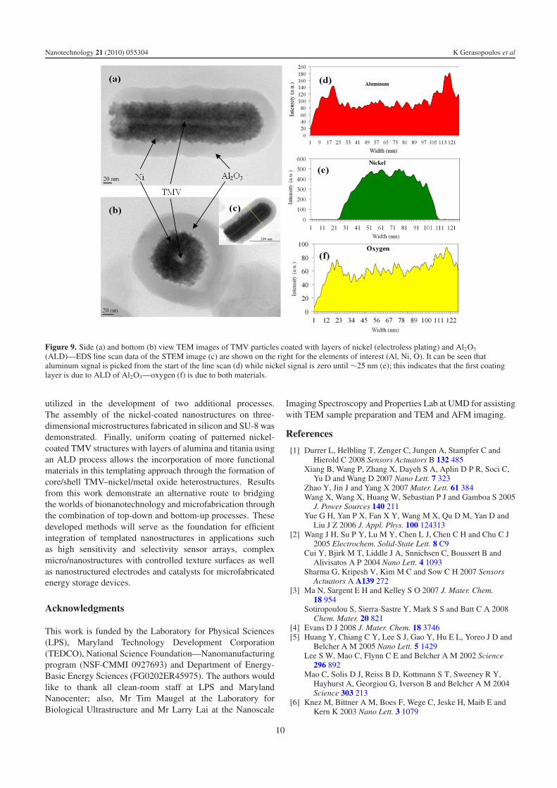
The coating uniformity was further investigated usingcross-sectional transmission electron microscopy (TEM).Figures 9(a) and (b) show the side and bottom view of an
individual TMV particle while figures 9(d)–(f) contain thecorresponding energy-dispersive x-ray spectroscopy (EDS)data of the particle in the inset (figure 9(c)). Oxygen is presentdue to both the Al2O3 as well as nickel that has been oxidized.The absence of any signal from nickel until approximately∼25 nm indicates the excellent coating uniformity of thealumina layer.
ALD has been previously employed by other researchersfor TMV coating. Knez et al demonstrated a roomtemperature deposition process for the decoration of TMV withlayers of alumina and titania [20]. In the work presentedhere, two significant advancements have been achieved.Deposition of composite materials on the nickel-coated virussurface expands the toolbox of available processes sincethe structure of the virus is entirely protected by the thinmetal coating thus allowing higher-temperature recipes to beapplied without structural degradation of the virus. Tuningof the layer thicknesses is also possible by adjusting thedeposition parameters for electroless plating and ALD steps.Additionally, the surface-attaching properties of the cysteine-modified TMV1cys as well as the photolithographic patterningcapability enable in situ synthesis of the desired materialswithout any requirement for post-integration in a device orsubstrate since the ALD and coated TMV lift-off processescould be combined for selective deposition of the films.
4. Conclusion
The development of novel fabrication methodologies forthe synthesis and patterning of nanostructured materialsusing the Tobacco mosaic virus was presented in thispaper. Metal-coated as well as uncoated TMV have beenlithographically patterned using a lift-off process that relies onselective photoresist and metal layer removal from a siliconsubstrate leaving the viruses on clearly-defined surfaces.Uncoated viruses maintain their chemical functionality afterfabrication which was verified through metallization with athin nickel layer. This fabrication approach is simple asit requires only one photolithography step and no particularsurface modification. It is versatile since it can beexpanded to multiple virus-templated materials while thewafer level scalability enables integration into high-throughputmanufacturing processes. The robustness of the metal-coated TMV templates and their patterning ability has been
9
Nanotechnology 21 (2010) 055304 K Gerasopoulos et al
Figure 9. Side (a) and bottom (b) view TEM images of TMV particles coated with layers of nickel (electroless plating) and Al2O3
(ALD)—EDS line scan data of the STEM image (c) are shown on the right for the elements of interest (Al, Ni, O). It can be seen thataluminum signal is picked from the start of the line scan (d) while nickel signal is zero until ∼25 nm (e); this indicates that the first coatinglayer is due to ALD of Al2O3—oxygen (f) is due to both materials.
utilized in the development of two additional processes.The assembly of the nickel-coated nanostructures on three-dimensional microstructures fabricated in silicon and SU-8 wasdemonstrated. Finally, uniform coating of patterned nickel-coated TMV structures with layers of alumina and titania usingan ALD process allows the incorporation of more functionalmaterials in this templating approach through the formation ofcore/shell TMV–nickel/metal oxide heterostructures. Resultsfrom this work demonstrate an alternative route to bridgingthe worlds of bionanotechnology and microfabrication throughthe combination of top-down and bottom-up processes. Thesedeveloped methods will serve as the foundation for efficientintegration of templated nanostructures in applications suchas high sensitivity and selectivity sensor arrays, complexmicro/nanostructures with controlled texture surfaces as wellas nanostructured electrodes and catalysts for microfabricatedenergy storage devices.
Acknowledgments
This work is funded by the Laboratory for Physical Sciences(LPS), Maryland Technology Development Corporation(TEDCO), National Science Foundation—Nanomanufacturingprogram (NSF-CMMI 0927693) and Department of Energy-Basic Energy Sciences (FG0202ER45975). The authors wouldlike to thank all clean-room staff at LPS and MarylandNanocenter; also, Mr Tim Maugel at the Laboratory forBiological Ultrastructure and Mr Larry Lai at the Nanoscale
Imaging Spectroscopy and Properties Lab at UMD for assistingwith TEM sample preparation and TEM and AFM imaging.
References
[1] Durrer L, Helbling T, Zenger C, Jungen A, Stampfer C andHierold C 2008 Sensors Actuators B 132 485
Xiang B, Wang P, Zhang X, Dayeh S A, Aplin D P R, Soci C,Yu D and Wang D 2007 Nano Lett. 7 323
Zhao Y, Jin J and Yang X 2007 Mater. Lett. 61 384Wang X, Wang X, Huang W, Sebastian P J and Gamboa S 2005
J. Power Sources 140 211Yue G H, Yan P X, Fan X Y, Wang M X, Qu D M, Yan D and
Liu J Z 2006 J. Appl. Phys. 100 124313[2] Wang J H, Su P Y, Lu M Y, Chen L J, Chen C H and Chu C J
2005 Electrochem. Solid-State Lett. 8 C9Cui Y, Bjirk M T, Liddle J A, Snnichsen C, Boussert B and
Alivisatos A P 2004 Nano Lett. 4 1093Sharma G, Kripesh V, Kim M C and Sow C H 2007 Sensors
Actuators A A139 272[3] Ma N, Sargent E H and Kelley S O 2007 J. Mater. Chem.
18 954Sotiropoulou S, Sierra-Sastre Y, Mark S S and Batt C A 2008
Chem. Mater. 20 821[4] Evans D J 2008 J. Mater. Chem. 18 3746[5] Huang Y, Chiang C Y, Lee S J, Gao Y, Hu E L, Yoreo J D and
Belcher A M 2005 Nano Lett. 5 1429Lee S W, Mao C, Flynn C E and Belcher A M 2002 Science
296 892Mao C, Solis D J, Reiss B D, Kottmann S T, Sweeney R Y,
Hayhurst A, Georgiou G, Iverson B and Belcher A M 2004Science 303 213
[6] Knez M, Bittner A M, Boes F, Wege C, Jeske H, Maib E andKern K 2003 Nano Lett. 3 1079
10

Nanotechnology 21 (2010) 055304 K Gerasopoulos et al
Knez M, Sumser M, Bittner A M, Wege C, Jeske H, Kooi S,Burghard M and Kern K 2002 J. Electroanal. Chem. 522 70
Knez M, Sumser M, Bittner A M, Wege C, Weske H,Martin T P and Kern K 2004 Adv. Funct. Mater. 14 116
Liou W L, Balandin A A, Mathews D M and Dodds J A 2005Appl. Phys. Lett. 86 253108
[7] Royston E, Lee S-Y, Culver J N and Harris M T 2006J. Colloid Interface Sci. 298 706
Lee S-Y, Royston E, Culver J N and Harris M T 2005Nanotechnology 16 S435
Royston E, Ghosh A, Kofinas P, Harris M T and Culver J N2007 Langmuir 24 906
Royston E, Brown A D, Harris M T and Culver J N 2009J.Colloid Interface Sci. 332 402
[8] Gerasopoulos K, McCarthy M, Royston E, Culver J N andGhodssi R 2008 J. Micromech. Microeng. 18 10
[9] Cheung C L, Camarero J A, Woods B W, Lin T, Johnson J Eand Yoreo J J D 2003 J. Am. Chem. Soc. 125 6848
Piner R D, Zhu J, Xu F, Hong S and Mirkin C A 1999 Science283 661
[10] Salaita K, Wang Y, Fragala J, Vega R A, Liu C and Mirkin C A2006 Angew. Chem. Int. Edn 45 7220
[11] Keren K, Krueger M, Gilad R, Ben-Yospeh G, Sivan U andBraun E 2002 Science 297 72
Rothemund P W K 2006 Nature 440 297[12] Yi H, Nisar S, Lee S-Y, Powers M A, Bentley W E, Payne G F,
Ghodssi R, Rubloff G W, Harris M T and Culver J N 2005Nano Lett. 5 1931
[13] Kuncicky D M, Naik R R and Velev O D 2006 Small 2 1462[14] Balci S, Leinberger D M, Knez M, Bittner A M, Boes F,
Kadri A, Wege C, Jeske H and Kern K 2008 Adv. Mater.20 2195
Bernard A, Renault J P, Michel B, Bosshard H R andDelamarche E 2000 Adv. Mater. 12 1067
[15] Yoo P J, Nam K T, Belcher A M and Hammond P T 2008 NanoLett. 8 1081
[16] Dawson W O, Beck D L, Knorr D A and Grantham G L 1986Proc. Natl Acad. Sci. 83 1832
[17] Gooding G V and Herbert T T 1967 Phytopathology 57 1285[18] Ott A W, Klaus J W, Johnson J M and George S M 2006 Thin
Solid Films 498 1–2[19] Spurr A R 1969 J. Ultrastruct. Res. 26 31[20] Knez M, Kadri A, Wege C, Gosele U, Jeske H and
Nielsch K 2006 Nano Lett. 6 1172
11