rapid and multi-step, patterned electrophoretic …iph1/download/lee--dbepd-apl-2014.pdfrapid and...
TRANSCRIPT

Rapid and multi-step, patterned electrophoretic deposition of nanocrystals usingelectrodes covered with dielectric barriersSeung Whan Lee, Datong Zhang, and Irving P. Herman
Citation: Applied Physics Letters 104, 053113 (2014); doi: 10.1063/1.4863849 View online: http://dx.doi.org/10.1063/1.4863849 View Table of Contents: http://scitation.aip.org/content/aip/journal/apl/104/5?ver=pdfcov Published by the AIP Publishing Articles you may be interested in Optimizing non-radiative energy transfer in hybrid colloidal-nanocrystal/silicon structures by controlled nanopillararchitectures for future photovoltaic cells Appl. Phys. Lett. 100, 021902 (2012); 10.1063/1.3675634 Fracture in electrophoretically deposited CdSe nanocrystal films J. Appl. Phys. 105, 103513 (2009); 10.1063/1.3118630 Photovoltaic cells fabricated by electrophoretic deposition of CdSe nanocrystals Appl. Phys. Lett. 93, 043504 (2008); 10.1063/1.2965464 Fabrication of Cu/Co bilayer gate electrodes using selective chemical vapor deposition and soft lithographicpatterning J. Appl. Phys. 100, 113705 (2006); 10.1063/1.2396796 Electrodeposition of patterned CdSe nanocrystal films using thermally charged nanocrystals Appl. Phys. Lett. 80, 3823 (2002); 10.1063/1.1480878
This article is copyrighted as indicated in the article. Reuse of AIP content is subject to the terms at: http://scitation.aip.org/termsconditions. Downloaded to IP:
128.59.65.231 On: Wed, 10 Sep 2014 16:29:32
Rapid and multi-step, patterned electrophoretic deposition of nanocrystalsusing electrodes covered with dielectric barriers
Seung Whan Lee, Datong Zhang, and Irving P. Hermana)
Department of Applied Physics and Applied Mathematics, Columbia University, New York,New York 10027, USA
(Received 11 December 2013; accepted 18 January 2014; published online 6 February 2014)
The rates of electrophoretic deposition (EPD) of CdSe nanocrystals (NCs) are approximately
the same when powering electrodes on either the frontside or backside of thick dielectrics when
the resistance of the NC colloid exceeds that of the dielectric barrier. Using electrodes with
dielectric barriers enables conformal coverage over topography on the frontside. It also enables
multistep processing when combined with powering patterned frontside electrodes for localized
EPD. Powering patterned backside electrodes produces film features that are wider than the
electrode dimensions, which is consistent with the results of modeling the electric field profile.VC 2014 AIP Publishing LLC. [http://dx.doi.org/10.1063/1.4863849]
Electrophoretic deposition (EPD) is a versatile method
in which DC electric fields are used to fabricate a wide range
of films,1,2 including those formed by depositing charged
nanocrystals (NCs) from a colloid. EPD using colloids of
charged NCs that are capped with organic ligands and in
nonpolar solvents forms films of distinct NCs.2,3 This can be
important for a range of applications, including the fabrica-
tion of light emitters and detectors, and photovoltaic devices
with semiconductor nanocrystals. EPD of charged nanopar-
ticles in polar solvents is often used to form films that are
later densified to produce uniform and dense ceramics or
composites.1
During EPD, the conducting electrode is usually in con-
tact with the colloidal solution (and so is on the “frontside”
of the electrode substrate). However, recent work has dem-
onstrated EPD where the conducting electrode is separated
from the colloid by a dielectric barrier. In one study, the con-
ducting pathway (a “buried” layer) was covered by a thin in-
sulator, 30 nm thick polystyrene films on Si, to enable EPD
of films of CdSe NCs.4 In another, the conducting electrode
was fabricated on the “backside” of 100 lm thick polytetra-
fluoroethylene (PTFE) (and so was not in contact with the
colloid) for EPD of poly-(3)hexylthiophene (P3HT) clusters
on the frontside.5 EPD with such buried or backside conduct-
ing electrodes, sometimes called dielectric barrier EPD
(DBEPD),5 has potential advantages of being able to deposit
directly on dielectrics, avoiding the undesired electrochemis-
try and heating that can occur on conducting surfaces. EPD
of nanoparticles (without molecular ligands) was demon-
strated on insulating porous layers6,7 (and possibly also on
insulating solid layers8). However, in this porous layer, the
conductivity path to the underlying conducting electrode was
maintained by charged species in the conducting solvent and
not electron transport through the dielectric or “insulator,” as
in DBEPD.
While these previous studies demonstrated that DBEPD
can occur, they did not address the key issues that can either
limit or expand near-term use of DBEPD. DBEPD would be
expected to be very slow compared to EPD with frontside
electrodes, because the large voltage drop across a dielectric
barrier would make the particle drift speed (which is propor-
tional to electric field and therefore the voltage drops across
the colloid) small and therefore the deposition rate would be
slow. The applied voltage and other conditions must be set
so the voltage drop across the colloid is large enough for fast
EPD, with the electric field in the dielectric being smaller
than the breakdown limit. We show that DBEPD of colloidal
NCs can be as fast as with frontside electrodes, even with
quite thick insulators, for very common EPD experimental
conditions. In addition, we show that this and the spatial re-
solution of patterned DBEPD can be understood by modeling
the electric field in the colloid and dielectric. We also dem-
onstrate versatile fabrication processes that utilize both front-
side and backside electrodes.
CdSe nanocrystals of 3.8–5.1 nm diameter capped with
phosphonates and trioctylphosphine oxide (TOPO) were syn-
thesized using the procedure in Ref. 9 but with two precursor
injections10 and were washed 3–5 times and then dispersed in
hexane solvent before EPD, as in Ref. 11. CdSe NC diameters
were determined using visible absorption spectroscopy, as has
been confirmed by transmission electron microscopy.12 The
electrode substrates were highly insulating, 1.2 mm thick glass
slides (Electron Microscopy Sciences). For the maximum
voltage used here, 3000 V, the maximum electric field in the
substrate (3000 V/1.2 mm¼ 2.5� 106 V/m) was much smaller
than the breakdown fields of glasses (�107–108 V/m). (No
evidence of breakdown was seen.) The frontsides of the elec-
trode substrates (�2 cm lateral dimensions) were in contact
with the colloid solution and separated by 2.5 cm by using a
cylindrical teflon chamber of this length and 2 cm inside diam-
eter; O-ring seals prevented leakage and contact of the solu-
tion with the backside of the substrate electrodes (Fig. 1(a)).
Unpatterned backside electrodes for DBEPD were made by
attaching �2 cm square piece of Cu/Ni tape (Ted Pella) to the
back of the glass. Unless otherwise specified, “Au” electrodes
were formed by thermal evaporation of 10 nm Cr/50 nm Au,
and the opposing electrode was an unpatterned frontside Au
a)Author to whom correspondence should be addressed. Electronic mail:
0003-6951/2014/104(5)/053113/4/$30.00 VC 2014 AIP Publishing LLC104, 053113-1
APPLIED PHYSICS LETTERS 104, 053113 (2014)
This article is copyrighted as indicated in the article. Reuse of AIP content is subject to the terms at: http://scitation.aip.org/termsconditions. Downloaded to IP:
128.59.65.231 On: Wed, 10 Sep 2014 16:29:32
electrode. Patterned Au electrodes were fabricated by pattern-
ing photoresist (Heidelberg lPG 101 Laser Writer), followed
by metal deposition and then liftoff, to form centrally
placed lines with the desired widths. EPD profiles were ana-
lyzed using scanning electron (SEM), optical, and atomic
force microscopies and profilometry. SEM was used to exam-
ine the transverse profiles after cross-sectioning the samples
(by cracking them).
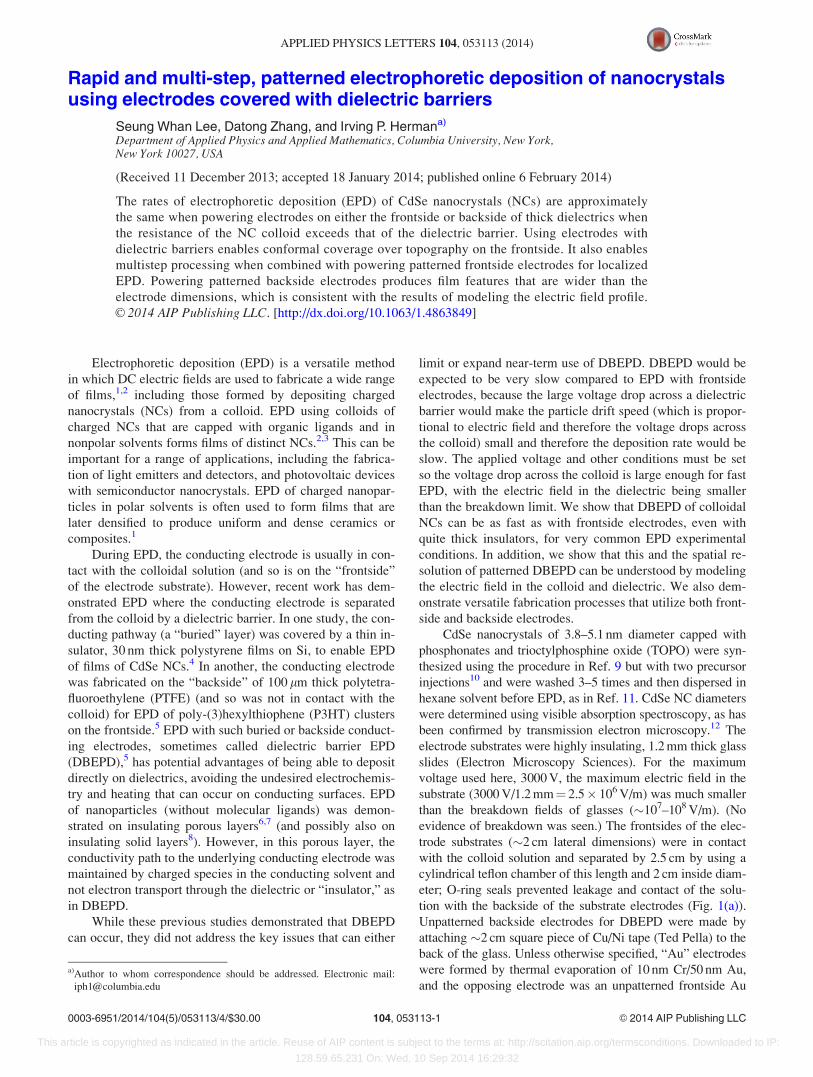
As seen in Fig. 1(c), similar DBEPD CdSe NC films
formed on the frontsides of both glass electrodes when
1000 V was applied for 30 min across unpatterned backside
electrodes and the colloid solution (with a �1.2� 1015/cm3
concentration of the 3.8 nm NCs, corresponding to
0.2 mg/ml). The circular shape of the films is determined by
the teflon assembly and not the, larger, backside electrodes.
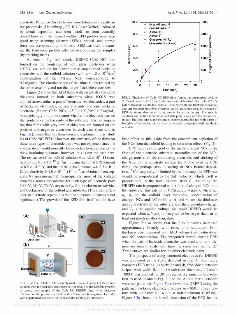
Figure 2 shows that EPD films with essentially the same
thickness formed on both substrates when 1000 V was
applied across either a pair of frontside Au electrodes, a pair
of backside electrodes, or one frontside and one backside
electrode (5.1 nm CdSe NCs, �5.0� 1014/cm3, 0.2 mg/ml),
so surprisingly, it did not matter whether the electrode was on
the frontside or the backside of the substrate. It is not surpris-
ing that films with very similar thickness are formed on the
positive and negative electrodes in each case (here and in
Fig. 1(c)), since this has been seen and explained in past stud-
ies of CdSe NC EPD.3 However, the similarity of the films for
these three types of electrode pairs was not expected since the
voltage drop would normally be expected to occur across the
thick insulating substrate; however, this is not the case here.
The resistance of the colloid solution was 1.2� 1011 X (con-
ductivity is 6.8� 10�10 X�1m�1, using the initial EPD current
of 8.5� 10�9 A) and that of the glass substrate was 3.7� 1010
X (conductivity is 1.0� 10�10 X�1m�1, as obtained from sep-
arate I-V measurements). Consequently, most of the voltage
drop was across the solution for each type of electrode pair:
1000 V, 610 V, 760 V, respectively, for the chosen resistivities
and thicknesses of the colloid and substrate. (The small differ-
ence in electrode separations due the substrate thickness is not
significant.) The growth of the EPD film itself should have
little effect on this, aside from the concomitant depletion of
the NCs from the colloid leading to saturation effects (Fig. 2).
EPD requires transport of thermally charged NCs to the
front of the electrode substrate, neutralization of the NCs,
charge transfer to the conducting electrode, and sticking of
the NCs to the substrate surface (or to the existing EPD
film), and perhaps also clustering of NCs before deposi-
tion.13 Consequently, if limited by the first step, the EPD rate
would be proportional to the drift velocity, which itself is
proportional to the local electric field E. Assuming the
DBEPD rate is proportional to the flux of charged NCs onto
the substrate, this rate is / Va/(dc/ncelcþ ds/rs), where dc,
nc, lc are the colloid layer thickness, concentration of
charged NCs and NC mobility, ds and rs are the thickness
and conductivity of the substrate, e is the elementary charge,
and Va is the applied voltage. So, rapid DBEPD would be
expected when dc/ncelc is designed to be larger than, or at
least not much smaller than, ds/rs.
Figure 2 also shows that the film thickness increased
approximately linearly with time, until saturation. Film
thickness also increased with EPD voltage (until saturation)
and NC concentration. The integrated current during EPD
when the pair of backside electrodes was used and the thick-
ness are seen to scale with time the same way in Fig. 2.3
These curves are similar for the other electrode pairs.
The prospects of using patterned electrodes for DBEPD
was addressed in the study depicted in Fig. 3. This figure
compares EPD using (a) backside and (b) frontside electrodes
stripes with width 0.1 mm (�substrate thickness, 1.2 mm).
1000 V was applied for 30 min across the same colloid solu-
tion as used to obtain Fig. 2, and the Au counter electrodes
were not patterned. Figure 3(a) shows that DBEPD using the
patterned backside electrode produces an �850 nm thick fea-
ture with �1.8 mm full-width at half-maximum (FWHM).
Figure 3(b) shows the lateral dimension of the EPD feature
FIG. 1. (a) The EPD/DBEPD assembly used to prevent contact of the colloid
solution with the backside electrodes; (b) schematic of the DBEPD process;
(c) optical micrographs of the CdSe NC DBEPD films (with thickness
�505 nm on the positive electrode and �565 nm on the negative electrode)
with unpatterned electrodes on the backsides of the glass substrates.
FIG. 2. Thickness of CdSe NC EPD films formed on unpatterned positive
(“P”) and negative (“N”) electrodes for a pair of frontside electrodes (“Au”),
pair of backside electrodes (“Glass”), or a pair with one frontside (negative)
and one backside (positive) electrode on the glass substrate, for a range of
EPD durations, determined using atomic force microscopy. The specific
electrode for the film is noted for each data point, along with the pair of elec-
trodes. The solid line is the integrated current during the run with a pair of
backside of electrodes, with a scale that enables comparison with the thick-
ness data.
053113-2 Lee, Zhang, and Herman Appl. Phys. Lett. 104, 053113 (2014)
This article is copyrighted as indicated in the article. Reuse of AIP content is subject to the terms at: http://scitation.aip.org/termsconditions. Downloaded to IP:
128.59.65.231 On: Wed, 10 Sep 2014 16:29:32
matches that of the patterned frontside electrode, as was also
seen in earlier work3 down to a width of 1 lm.
To understand Fig. 3(a), we modeled the electric field Eon the top of the glass using a two-dimensional steady-state
finite-difference model of Ohm’s Law, J¼ rE, and the conti-
nuity of current equation in steady state, @q/@t¼�$�J¼ 0,
where r is the conductivity and q and J are the charge and
current densities. This is justified because steady state current
flow dominates essentially throughout EPD, since the RC con-
stants of the colloid and glass substrate are relatively short,
�0.024 s and 0.58 s, respectively (using the dielectric con-
stants for the hexane solvent, 1.8, and the glass electrode, 6.7).
Figure 3(a) shows that the profiles of the normal compo-
nents and magnitudes of E at the top surface of the glass slide
(Enormal FWHM ¼ 2.2 mm, Emagnitude FWHM¼ 3.7 mm). They
are much broader than the electrode, as would be expected
between line and plate electrodes in a line/plane capacitor.
The E field profile widths match the EPD profile well, with
the normal component fitting better, so this is consistent with
the general mechanism of EPD. (With this approximately
line-plane geometry, E, 3.6� 104 V/m, exceeds that with an
unpatterned backside electrode, 3.0� 104 V/m, even though
the voltage drop across the colloid, 170 V in the middle of
the substrate, is smaller than that with an unpatterned elec-
trode, 760 V.)
DBEPD can preserve pattern resolution only when the
dielectric barriers are relatively thin. Calculations show
that for a backside electrode feature of width w¼ 0.1 mm
¼ 100 lm, the FWHM of Enormal on the frontside increases
linearly from �2w to 4w for (glass) dielectric thicknesses
ranging from 0.5w to 2w (for this electrode arrangement).
Also, pattern resolution cannot be preserved much better by
changing colloid conductivity. Starting with the conditions of
Fig. 3(a), this FWHM decreases to 2.1 mm (from 2.2 mm)
when the conductivity is increased by either 10� or 100�; it
increases with decreasing conductivity first slowly, to 2.7 mm
when the conductivity is decreased by 10�, and then faster to
13.2 mm when it is decreased by 100�.
Conformal coverage of topography on the substrate
frontside by DBEPD would add a new dimension to potential
applications of EPD. Figure 4 demonstrates conformal cov-
erage over two different types of 5 lm wide lines on the sub-
strate frontside, by using two different types of DBEPD
processes, both with unpatterned backside electrodes and
unpatterned frontside counter electrodes. The SEMs of the
cross-sectioned samples in Figs. 4(b) and 4(c) show
FIG. 3. Optical micrographs of CdSe
NC EPD using 0.1 mm wide patterned
line electrodes on the (a) backside and
(b) frontside of the glass substrate
(positive electrode), along with the
profilometer trace and, for (a), the cal-
culated electric field profiles on the
frontside.
FIG. 4. (a) Schematic of unpatterned CdSe NC DBEPD over frontside topography, a 350 nm thick, 5 lm wide Cr/Au stripe, with scanning electron micro-
graphs of the cross-sectioned substrate, showing blanketed conformal coverage by (b) �360 nm and (c) �1850 nm thick CdSe NC DBEPD films. (d)
Schematic of local EPD of CdSe NCs on a patterned 350 nm thick, 5 lm wide Cr/Au stripe, followed by unpatterned DBEPD of P3HT over this frontside to-
pography, with (e) scanning electron micrograph of the cross-sectioned substrate, showing a �1200 nm thick DBEPD P3HT film conformally covering a
�300 nm thick local EPD deposit of CdSe NCs atop the 5 lm wide Cr/Au stripe. (The film asymmetry was caused by the patterning step.)
053113-3 Lee, Zhang, and Herman Appl. Phys. Lett. 104, 053113 (2014)
This article is copyrighted as indicated in the article. Reuse of AIP content is subject to the terms at: http://scitation.aip.org/termsconditions. Downloaded to IP:
128.59.65.231 On: Wed, 10 Sep 2014 16:29:32

blanketed, conformal coverage over �350 nm high frontside
topography (300 nm Cr/50 nm Au stripe) on the positive
electrode by relatively thin (�360 nm) and thick (�1850 nm)
films of CdSe NCs, respectively, formed by using the
approach illustrated in Fig. 4(a). This was done by using
4.0 nm CdSe NC colloids (�2.6� 1015 NCs/cm3, 0.5 mg/ml
in (b) and �6.7� 1015 NCs/cm3, 1.3 mg/ml in (c)), with
1000 V applied for 30 min. The SEM of the cross-sectioned
sample in Fig. 4(e) shows conformal coverage by
a� 1200 nm thick P3HT film (from P3HT clusters14) by
DBEPD, by using the unpatterned backside electrode, over
a� 300 nm thick CdSe NC EPD film that had first been
selectively deposited on �350 nm high frontside topography
(300 nm Cr/50 nm Au stripe), as is illustrated in Fig. 4(d).
For the CdSe NC EPD, 300 V was applied for 3 min using
the substrate as the positive electrode as in Figs. 4(b) and
4(c) (4.0 nm, 5.1� 1015 NCs/cm3, 1.0 mg/ml). For the P3HT
DBEPD, 3000 V was applied for 120 min powering the same
substrate as negative electrode, as is necessary for P3HT,
using 2.4 mg P3HT (from Lumtec (LT-S909, MW> 45 000
Daltons)) first dispersed in 30 ml toluene, and then diluted
with 20 ml hexane.5
Because of this conformal coverage, a combination of
an unpatterned backside electrode and several distinct pat-
terned frontside electrodes can be the building blocks for
fabricating discretionary 3D, multi-layer structures of differ-
ent NCs (or materials such as conducting polymers) by alter-
nately powering one of a series of electrodes with different
solutions present, as is illustrated in Figs. 4(d) and 4(e).
In conclusion, DBEPD rates can be fast with carefully
designed geometry and colloid conditions, and the coverage
is conformal. 3D multi-level discretionary structures can be
fabricated using multi-step EPD, by alternately powering
patterned frontside, and patterned or unpatterned backside
electrodes for a variety of dielectrics, including flexible sub-
strates. More functionality can be added by utilizing several
existing techniques, such as those used in the EPD of mix-
tures of different NCs15,16 and of functionally graded
materials.16 Transfer of these findings from nonpolar to polar
and aqueous colloid solutions requires the use of lower vol-
tages (on the order of volts) to avoid solution electrochemis-
try; with the much higher conductivity of these solutions, the
fields in the colloids would be much smaller.
This material is primarily based upon work supported as
part of the Center for Re-Defining Photovoltaic Efficiency
through Molecule Scale Control, an Energy Frontier
Research Center funded by the U.S. Department of Energy,
Office of Science, Office of Basic Energy Sciences under
Award Number DE-SC0001085. This work is also supported
by a matching grant from the Empire State Development’s
Division of Science, Technology and Innovation
(NYSTAR). The authors would like to thank Dae In Kim for
his help in photolithography.
1L. Besra and M. Liu, Prog. Mater. Sci. 52, 1 (2007).2Electrophoretic Deposition of Nanomaterials, edited by J. H. Dickerson
and A. R. Boccaccini (Springer, New York, 2011).3M. Islam and I. P. Herman, Appl. Phys. Lett. 80, 3823 (2002).4S. A. Hasan, D. W. Kavich, S. V. Mahajan, and J. H. Dickerson, Thin
Solid Films 517, 2665 (2009).5S. Miyajima, S. Nagamatsu, S. S. Pandey, S. Hayase, K. Kaneto, and W.
Takashima, Appl. Phys. Lett. 101, 193305 (2012).6M. Matsuda, T. Hosomi, K. Murata, T. Fukui, and M. Miyake,
Electrochem. Solid State Lett. 8, A8 (2005).7L. Besra, C. Compson, and M. L. Liu, J. Am. Ceram. Soc. 89, 3003
(2006).8L. Besra, S. Zha, and M. Liu, J. Power Sources 160, 207 (2006).9C. B. Murray, D. J. Norris, and M. G. Bawendi, J. Am. Chem. Soc. 115,
8706 (1993).10Z. A. Peng and X. Peng, J. Am. Chem. Soc. 124, 3343 (2002).11M. A. Islam, Y. Xia, D. A. Telesca, Jr., M. L. Steigerwald, and I. P.
Herman, Chem. Mater. 16, 49 (2004).12W. W. Yu, L. Qu, W. Guo, and X. Peng, Chem. Mater. 15, 2854 (2003).13S. Jia, S. Banerjee, and I. P. Herman, J. Phys. Chem. C 112, 162 (2008).14K. Tada and M. Onoda, Thin Solid Films 438–439, 365 (2003).15M. A. Islam, Y. Xia, M. L. Steigerwald, M. Yin, Z. Liu, S. O’Brien, R.
Levicky, and I. P. Herman, Nano Lett. 3, 1603 (2003).16S. Put, J. Vleugels, and O. Van Der Biest, Acta Mater. 51, 6303 (2003).
053113-4 Lee, Zhang, and Herman Appl. Phys. Lett. 104, 053113 (2014)
This article is copyrighted as indicated in the article. Reuse of AIP content is subject to the terms at: http://scitation.aip.org/termsconditions. Downloaded to IP:
128.59.65.231 On: Wed, 10 Sep 2014 16:29:32