battery charger system with integrated power switch … is information on a product in full...
TRANSCRIPT

This is information on a product in full production.
September 2017 DocID11908 Rev 10 1/41
L6924D
Battery charger system with integrated power switch for Li-Ion/Li-Polymer
Datasheet - production data
Features Fully integrated solution, with a power
MOSFET, reverse blocking diode, sense resistor, and thermal protection
Ideal for coke and graphite anode single-cell LI-ION packs
Both linear and quasi-pulse operation Closed loop thermal control USB BUS-compatible Programmable charge current up to 1 A Programmable pre-charge current Programmable end-of-charge current Programmable pre-charge voltage threshold Programmable charge timer Programmable output voltage at 4.1 V and
4.2 V, with ± 1 % output voltage accuracy (NTC) or (PTC) thermistor interface for battery
temperature monitoring and protection Flexible charge process termination Status outputs to drive LEDs or to interface
with a host processor Small VFQFPN 16-lead package (3 x 3 mm)
Applications Handheld devices Digital cameras Standalone chargers USB-powered chargers
VFQFPN16 Table 1. Device summaryOrder code Package Packaging
L6924D013TR VFQFPN16 Tape and reel
www.st.com

Contents L6924D
2/41 DocID11908 Rev 10
Contents
1 Description . . . . . . . . . . . . . . . . . . . . . . . . . . . . . . . . . . . . . . . . . . . . . . . . . 4
2 Pin description and connection diagrams . . . . . . . . . . . . . . . . . . . . . . . 52.1 Pin description . . . . . . . . . . . . . . . . . . . . . . . . . . . . . . . . . . . . . . . . . . . . . . 5
3 Maximum ratings . . . . . . . . . . . . . . . . . . . . . . . . . . . . . . . . . . . . . . . . . . . . 73.1 Absolute maximum ratings . . . . . . . . . . . . . . . . . . . . . . . . . . . . . . . . . . . . . 7
3.2 Thermal data . . . . . . . . . . . . . . . . . . . . . . . . . . . . . . . . . . . . . . . . . . . . . . . 7
4 Electrical specifications . . . . . . . . . . . . . . . . . . . . . . . . . . . . . . . . . . . . . . 84.1 Electrical characteristics . . . . . . . . . . . . . . . . . . . . . . . . . . . . . . . . . . . . . . . 8
5 Block diagram . . . . . . . . . . . . . . . . . . . . . . . . . . . . . . . . . . . . . . . . . . . . . 10
6 Operation description . . . . . . . . . . . . . . . . . . . . . . . . . . . . . . . . . . . . . . . 116.1 Linear mode . . . . . . . . . . . . . . . . . . . . . . . . . . . . . . . . . . . . . . . . . . . . . . . 12
6.2 Quasi-pulse mode . . . . . . . . . . . . . . . . . . . . . . . . . . . . . . . . . . . . . . . . . . 14
7 Application information: charging process . . . . . . . . . . . . . . . . . . . . . 177.1 Charging process flow chart . . . . . . . . . . . . . . . . . . . . . . . . . . . . . . . . . . . 17
7.2 Pre-charge current . . . . . . . . . . . . . . . . . . . . . . . . . . . . . . . . . . . . . . . . . . 18
7.3 Pre-charge voltage . . . . . . . . . . . . . . . . . . . . . . . . . . . . . . . . . . . . . . . . . . 18
7.4 Fast charge current . . . . . . . . . . . . . . . . . . . . . . . . . . . . . . . . . . . . . . . . . 19
7.5 End-of-charge current . . . . . . . . . . . . . . . . . . . . . . . . . . . . . . . . . . . . . . . 20
7.6 Recharge flow chart . . . . . . . . . . . . . . . . . . . . . . . . . . . . . . . . . . . . . . . . . 21
7.7 Recharge threshold . . . . . . . . . . . . . . . . . . . . . . . . . . . . . . . . . . . . . . . . . 21
7.8 Maximum charging time . . . . . . . . . . . . . . . . . . . . . . . . . . . . . . . . . . . . . . 22
7.9 Termination modes . . . . . . . . . . . . . . . . . . . . . . . . . . . . . . . . . . . . . . . . . . 23
8 Application information: monitoring and protection . . . . . . . . . . . . . . 248.1 NTC thermistor . . . . . . . . . . . . . . . . . . . . . . . . . . . . . . . . . . . . . . . . . . . . . 24
8.2 Battery absence detection . . . . . . . . . . . . . . . . . . . . . . . . . . . . . . . . . . . . 28
8.3 Status pins . . . . . . . . . . . . . . . . . . . . . . . . . . . . . . . . . . . . . . . . . . . . . . . . 29

DocID11908 Rev 10 3/41
L6924D Contents
41
8.4 Shutdown . . . . . . . . . . . . . . . . . . . . . . . . . . . . . . . . . . . . . . . . . . . . . . . . . 30
9 Additional application information . . . . . . . . . . . . . . . . . . . . . . . . . . . . 319.1 Selecting the input capacitor . . . . . . . . . . . . . . . . . . . . . . . . . . . . . . . . . . 31
9.2 Selecting the output capacitor . . . . . . . . . . . . . . . . . . . . . . . . . . . . . . . . . 31
9.3 Battery floating voltage setup . . . . . . . . . . . . . . . . . . . . . . . . . . . . . . . . . . 329.3.1 Battery floating voltage: VFLOAT . . . . . . . . . . . . . . . . . . . . . . . . . . . . . . . . . . . . . . .33
9.4 Layout guidelines and demonstration board description . . . . . . . . . . . . . 33
10 Application ideas . . . . . . . . . . . . . . . . . . . . . . . . . . . . . . . . . . . . . . . . . . . 3710.1 USB battery charger . . . . . . . . . . . . . . . . . . . . . . . . . . . . . . . . . . . . . . . . . 37
11 Package information . . . . . . . . . . . . . . . . . . . . . . . . . . . . . . . . . . . . . . . . 3811.1 VFQFPN16 package information . . . . . . . . . . . . . . . . . . . . . . . . . . . . . . . 39
12 Revision history . . . . . . . . . . . . . . . . . . . . . . . . . . . . . . . . . . . . . . . . . . . 40

Description L6924D
4/41 DocID11908 Rev 10
1 Description
The L6924D is a fully monolithic battery charger dedicated to single-cell Li-Ion/Polymer battery packs. It is the ideal solution for space-limited applications, like handheld equipment, and digital cameras. It integrates all of the power elements (the power MOSFET, reverse blocking diode and the sense resistor) in a small VFQFPN16 (3 x 3 mm) package. When an external voltage-regulated wall adapter is used, the L6924D works in linear mode, and charges the battery in a constant current/constant voltage (CC/CV) profile. Moreover, when a current-limited adapter is used, the device can operate in quasi-pulse mode, dramatically reducing the power dissipation. Regardless of the charging approach, a closed-loop thermal control avoids device overheating. The device has an operating input voltage ranging from 2.5 V to 12 V. The L6924D allows the user to program many parameters, such as pre-charge current, fast-charge current, pre-charge voltage threshold, end-of-charge current threshold, and charge timer. The L6924D offers two open collector outputs for diagnostic purposes, which can be used to either drive two external LEDs or communicate with a host microcontroller. Finally, the L6924D also provides very flexible control of the charge process termination and gas gauge capability, as well as other functions, such as checking for battery presence, and monitoring and protecting the battery from unsafe thermal conditions.
Figure 2. Basic application schematic
Figure 1. Minimum application size

DocID11908 Rev 10 5/41
L6924D Pin description and connection diagrams
41
2 Pin description and connection diagrams
Figure 3. Pin connections (top view)
2.1 Pin descriptionTable 2. Pin functions
Pin I/O Name Pin description
1 I VIN Input pin of the power stage.
2 I VINSNSSupply voltage pin of the signal circuitry.The operating input voltage ranges from 2.5 V to 12 V and the start-up threshold is 4 V.
3-4 O ST2-ST1 Open-collector status pins.
5 I TPRG
Maximum charging time program pin.It must be connected with a capacitor to GND to fix the maximum charging time, see Chapter 7.8: Maximum charging time on page 22
6 - GND Ground pin.
7 I SD Shutdown pin.When connected to GND enables the device; when floating disables the device.
8 I TH
Temperature monitor pin.It must be connected to a resistor divider including an NTC or PTC resistor. The charge process is disabled if the battery temperature (sensed through the NTC or PTC) is out of the programmable temperature window see Chapter 8.1: NTC thermistor on page 24.
9 I VOPRGOutput voltage selection pin. VOUT
= 4.1 V if left floating. VOUT = 4.2 V if connected to GND.
10 I VOSNSOutput voltage sense pin.It senses the battery voltage to control the voltage regulation loop.
11 O VOUT Output pin. (connected to the battery)

Pin description and connection diagrams L6924D
6/41 DocID11908 Rev 10
12 O VREF External reference voltage pin.(reference voltage is 1.8 V±2%)
13 I/O IEND
Charge termination pin.A resistor connected from this pin to GND fixes the charge termination current threshold IENDTH: if I < IENDTH, the charger behaves according to the VPRE
status (see Chapter 7.5: End-of-charge current on page 20). The voltage across the resistor is proportional to the current delivered to the battery (Gas Gauge function).
14 I VPRE
Multifunction pin.A resistor connected to GND allows the user to adjust the pre-charge voltage threshold VPRETH.If the pin is floating, VPRETH = 2.8 V. If the voltage on VPRE pin is lower than 0.8 V, VPRETH = 2.8 V and the charge is not automatically terminated when I < IENDTH.If the voltage on VPRE goes lower than 0.5 V (edge sensitive), the maximum charging time is reset.
15 I IPRG
Charge current program pin.A resistor connected from this pin to GND, fixes the fast charge current value (ICHG), with an accuracy of 7%.
16 I IPRE
Pre-charge current program pin.If the pin is floating IPRETH is equal to 10% of ICHG. If IPRETH has to be programmed at a different value, the pin has to be connected to GND or VREF
, through a resistor see Chapter 7.2: Pre-charge current on page 18.
Table 2. Pin functions

DocID11908 Rev 10 7/41
L6924D Maximum ratings
41
3 Maximum ratings
Stressing the device above the rating listed in the “absolute maximum ratings” table may cause permanent damage to the device. These are stress ratings only and operation of the device at these or any other conditions above those indicated in the operating sections of this specification is not implied. Exposure to absolute maximum rating conditions for extended periods may affect device reliability.
3.1 Absolute maximum ratings
3.2 Thermal data
Table 3. Absolute maximum ratingsSymbol Parameter Value Unit
VIN Input voltage –0.3 to 16 V
VINSNS, SD Input voltage –0.3 to VIN V
VOUT, VOSNS Output voltage –0.3 to 5 V
ST1, ST2Output voltage –0.3 to 6 V
Output current 30 mA
VREF, TH, IEND, IPRG, VPRE, IPRE, VOPRG,
TPRG, GND–0.3 to 4 V
ST1 and TH pins Maximum withstanding voltage range test condition: CDFAEC-Q100-002 (Normal “human body model” acceptance criteria performance)
±1.5 kV
Other pins ±2 kV
Table 4. Thermal dataSymbol Parameter Value Unit
RthJA Thermal resistance junction to ambient (1)
1. Device mounted on demonstration board
75 °C/W
TSTG Storage temperature range –55 to 150 °C
TJ Junction temperature range –40 to 125 °C
PTOT Power dissipation at T= 70 °C 0.67 W

Electrical specifications L6924D
8/41 DocID11908 Rev 10
4 Electrical specifications
4.1 Electrical characteristicsTJ = 25 °C, VIN = 5 V, unless otherwise specified.
Table 5. Electrical characteristics Symbol Parameter Test condition Min Typ Max Unit
VIN(1)
Operating input voltage 2.5 12 V
Start up threshold 4.1 V
IIN(1) Supply currentCharging mode (RPRG = 24k) 1.8 2.5 mA
Shutdown mode (RPRG = 24k) 60 80 μA
ISINK Current flowing from VOUT
Shutdown mode (RPRG = 24k) 500 nA
Stand by mode (RPRG = 24k)(VIN = 2.5V < VBATTERY)
500 nA
VOUT(1) Battery regulated voltage
VOPRG at VIN 4.06 4.1 4.14 V
VOPRG at GND 4.16 4.2 4.24 V
ICHG Charge currentRPRG = 24k 450 490 525 mA
RPRG = 12k 905 975 1045 mA
IPRECHPre-Charge current[default value = 10% ICHG]
IPRE floating
RPRG = 24k41 49 56 mA
IPRECH Pre-Charge currentRPRE = 62k to GND;RPRG = 24k
57 67 78 mA
IPRECH Pre-Charge currentRPRE = 39k to VREF;RPRG = 24k
29.5 35 40.1 mA
VPRETHPre-Charge voltage threshold [default] VPRE = VPRETHDefault = Floating 2.7 2.8 2.9 V
VPRETH Pre-Charge voltage threshold RVPRE = 13k; RPRG = 12k 2.87 3.03 3.19 V
VPRETH
Pre-Charge voltage threshold [default]. Charge termination disabled
2.7 2.8 2.9 V
IENDTH Termination current REND = 3K3 12 16 20 mA
TMAXCH(2) Maximum charging time
CTPRG = 10nFR[IPRG] = 24k
3 hours
TMAXCH(2)
Maximum charging time accuracyCTPRG = 5.6nFRPRG = 24k
10%
SDTHShutdown threshold high 2 V
Shutdown threshold low 0.4 V
ST1,2 Output status sink current Status on 10 mA
RDS(on) Power MOSFET resistance RDS(on)@ICHG = 500mA 280 380 m

DocID11908 Rev 10 9/41
L6924D Electrical specifications
41
TH NTC pin hot threshold voltage 10.625 12.5 14.375 %VREF
NTC pin cold threshold voltage 45 50 55 %VREF
1. TJ from –40°C to 125°C.
2. Guaranteed by design.
Table 5. Electrical characteristics (continued)Symbol Parameter Test condition Min Typ Max Unit
Block diagram L6924D
10/41 DocID11908 Rev 10
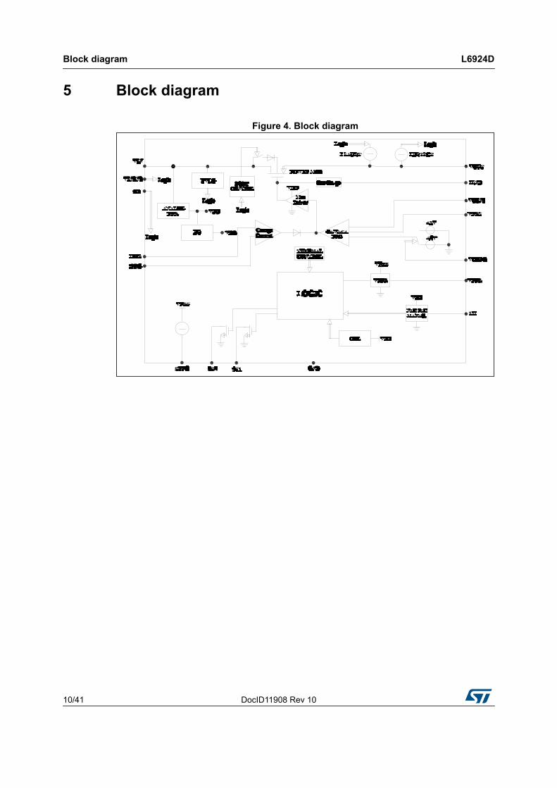
5 Block diagram
Figure 4. Block diagram

DocID11908 Rev 10 11/41
L6924D Operation description
41
6 Operation description
The L6924D is a fully integrated battery charger that allows a very compact battery management system for space limited applications. It integrates in a small package, all the power elements: power MOSFET, reverse blocking diode and the sense resistor.
It normally works as a linear charger when powered from an external voltage regulated adapter. However, thanks to its very low minimum input voltage (down to 2.5 V) the L6924D can also work as a Quasi-Pulse charger when powered from a current limited adapter. To work in this condition, is enough to set the device’s charging current higher than the adapter’s one (Chapter 7.4 on page 19). The advantage of the linear charging approach is that the device has a direct control of the charging current and so the designer needn’t to rely on the upstream adapter. However, the advantage of the Quasi-Pulse approach is that the power dissipated inside the portable equipment is dramatically reduced.
The L6924D charges the battery in three phases: Pre-Charge constant current: in this phase (active when the battery is deeply
discharged) the battery is charged with a low current. Fast-Charge constant current: in this phase the device charges the battery with the
maximum current. Constant Voltage: when the battery voltage reaches the selected output voltage, the
device starts to reduce the current, until the charge termination is done.
The full flexibility is provided by: Programmable pre-charging current and voltage thresholds (IPRETH and VPRETH)
(Chapter 7.2 on page 18, Chapter 7.3 on page 18). Programmable fast-charging current (ICHG) (Chapter 7.4 on page 19). Programmable end of charge current threshold (IENDTH) (Chapter 7.5 on page 20). Programmable end of charge timer (TMAXCH) (Chapter 7.8 on page 22).
If the full flexibility is not required and a smaller number of external components is preferred, default values of IPRETH and VPRETH are available leaving the respective pins floating. If a PTC or NTC resistor is used, the device can monitor the battery temperature in
order to protect the battery from operating in unsafe thermal conditions. Beside the good thermal behavior guaranteed by low thermal resistance of the
package, additional safety is provided by the built-in temperature control loop. The IC monitors continuously its junction temperature. When the temperature reaches approximately 120°C, the thermal control loop starts working, and reduces the charging current, in order to keep the IC junction temperature at 120°C.
Two open collector outputs are available for diagnostic purpose (status pins ST1 and ST2). They can be also used to drive external LEDs or to interface with a microcontroller.
The voltage across the resistor connected between IEND and GND gives information about the actual charging current (working as a Gas Gauge), and it can be easily fed into a μC ADC.

Operation description L6924D
12/41 DocID11908 Rev 10
When the VPRE pin is not used to program the Pre-Charge voltage threshold, it has two different functions: If the voltage across VPRE pin is lower than 0.8 V, when I < IENDTH, the end of charge is
notified by the status pin, but the charging process is not disabled. The charge process ends when the maximum charging time expires.
If the voltage at VPRE pin false under 0.5 V the timer is reset on the falling edge.
Battery disconnection control is provided thanks to the differentiated sensing and forcing output pins. A small current is sunk and forced through VOUT. If VOSNS doesn’t detect the battery, the IC goes into a standby mode.
Figure 5 shows the real charging profile of a Li-Ion battery, with a fast charge current of 450 mA (RPRG = 26 k),
Figure 5. Li-Ion charging profile
6.1 Linear modeWhen operating in linear mode, the device works in a way similar to a linear regulator with a constant current limit protection.
It charges the battery in three phases: Pre-charging current (“Pre-Charge” phase). Constant current (“Fast-Charge” phase). Constant voltage (“Voltage Regulation” phase).
VADP is the output voltage of the upstream AC-DC adapter that is, in turn, the input voltage of the L6924D. If the battery voltage is lower than a set pre-charge voltage (VPRETH), the pre-charge phase takes place. The battery is pre-charged with a low current IPRE (Chapter 7.2 on page 18).
When the battery voltage goes higher than VPRETH, the battery is charged with the fast charge current ICHG, set through an external resistor (Chapter 7.4 on page 19).

DocID11908 Rev 10 13/41
L6924D Operation description
41
Finally, when the battery voltage is close to the regulated output voltage VOPRGTH (4.1 V or 4.2 V), the voltage regulation phase takes place and the charging current is reduced. The charging process is usually terminated when the charging current reaches a set value or when a charging timer expires (Chapter 7.9 on page 23).
Figure 6 shows the different phases.
Figure 6. Typical charge curves in linear mode
The worst case in power dissipation occurs when the device starts the fast-charge phase. In fact, the battery voltage is at its minimum value. In this case, this is the maximum difference between the adapter voltage and battery voltage, and the charge current is at its maximum value.
The power dissipated is given by the following equation:
Equation 1
The higher the adapter voltage is, the higher the power dissipated. The maximum power dissipated depends on the thermal impedance of the device mounted on board.

Operation description L6924D
14/41 DocID11908 Rev 10
6.2 Quasi-pulse modeThe quasi-pulse mode can be used when the system can rely on the current limit of the upstream adapter to charge the battery. In this case, ICHG must be set higher than the current limit of the adapter. In this mode, the L6924D charges the battery with the same three phases as in linear mode, but the power dissipation is greatly reduced as shown in Figure 7.
Figure 7. Typical charge curves in quasi pulse mode
The big difference is due to the fact that ICHG is higher than the current limit of the adapter. During the fast-charge phase, the output voltage of the adapter drops and goes down to the battery voltage plus the voltage drop across the power MOSFET of the charger, as shown in the following equation:
Equation 2

DocID11908 Rev 10 15/41
L6924D Operation description
41
Where VMOS is given by:
Equation 3
Where,ILIM = current limit of the wall adapter, and RDS(on) = resistance of the power MOSFET.
The difference between the set charge current and the adapter limit should be high enough to minimize the RDS(on) value (and the power dissipation). This makes the control loop completely unbalanced and the power element is fully turned on.
Figure 8 shows the RDS(on) values for different output voltage and charging currents for an adapter current limit of 500 mA.
Figure 8. RDS(on) curves vs charging current and output voltage
Neglecting the voltage drop across the charger (VMOS) when the device operates in this condition, its input voltage is equal to the battery one, and so a very low operating input voltage (down to 2.5 V) is required. The power dissipated by the device during this phase is:
Equation 4

Operation description L6924D
16/41 DocID11908 Rev 10
When the battery voltage approaches the final value, the charger gets back the control of the current, reducing it. Due to this, the upstream adapter exits the current limit condition and its output goes up to the regulated voltage VADP. This is the worst case in power dissipation:
Equation 5
In conclusion, the advantage of the linear charging approach is that the designer has the direct control of the charge current, and consequently the application can be very simple. The drawback is the high power dissipation.
The advantage of the Quasi-Pulse charging method is that the power dissipated is dramatically reduced. The drawback is that a dedicated upstream adapter is required.
DocID11908 Rev 10 17/41
L6924D Application information: charging process
41
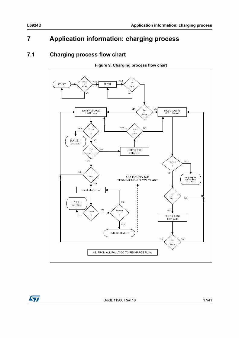
7 Application information: charging process
7.1 Charging process flow chart
Figure 9. Charging process flow chart

Application information: charging process L6924D
18/41 DocID11908 Rev 10
7.2 Pre-charge currentThe L6924D allows pre-charging the battery with a low current when the battery voltage is lower than a specified threshold (VPRETH). The Pre-charge current has a default value equal to 10% of the fast-charge current. However it can be adjusted by connecting a resistor from the IPRE pin to GND or VREF (see Figure 10). When the resistor is connected between IPRE pin and GND, the current is higher than the default value. The RPRE value is given by:
Equation 6
Figure 10. IPRE pin connection
When RPRE is connected to VREF, the current is lower than the default value. VREF is the external reference equal to 1.8 V, VBG is the internal reference equal to 1.23 V and KPRE is a constant equal to 950. See Figure 11.
The relationship is shown in the equation 7:
Equation 7
Figure 11. IPRE pin connection
7.3 Pre-charge voltageIf the VPRE pin is floating, a default value of VPRETH is set, equal to 2.8 V (VPRETHDefault). Otherwise, the device offers the possibility to program this value, with a resistor connected

DocID11908 Rev 10 19/41
L6924D Application information: charging process
41
between the VPRE pin and GND (see Figure 12). In this case, the RVPRE is given by the equation 8:
Equation 8
Figure 12. VPRE pin connection
Where RVPRE is the resistor between VPRE and GND, and RPRG is the resistor used to set the charge current (see Section 7.4: Fast charge current), and VPRETH is the selected threshold.
A safety timer is also present. If the battery voltage doesn't rise over VPRETH, before this time is expired, a fault is given (see Section 7.8: Maximum charging time). If at the beginning of the charge process, the battery voltage is higher than the VPRETH, the Pre-Charge phase is skipped.
7.4 Fast charge currentWhen the battery voltage reaches the Pre-charge voltage threshold (VPRETH), the L6924D starts the Fast-charge Phase. In this phase, the device charges the battery with a constant current, ICHG, programmable by an external resistor that sets the charge current with an accuracy of 7% Figure 13. The equation used to select the RPRG as follows:
Equation 9
Figure 13. IPRG pin connection
Where KPRG is a constant, equal to 9500.

Application information: charging process L6924D
20/41 DocID11908 Rev 10
During this phase, the battery voltage increases until it reaches the programmed output voltage. A safety timer is also present. If this time expires, a fault is given (Section 7.8: Maximum charging time).
7.5 End-of-charge currentWhen the charge voltage approaches the selected value (4.1 V or 4.2 V), the voltage regulation phase takes place. The charge current starts to decrease until it goes lower than a programmable end value, IENDTH, depending on an external resistor connected between the IEND pin and GND (see Figure 14). The equation that describes this relation as follows:
Equation 10
Figure 14. IEND pin connection
Where KEND is 1050; and VMIN is 50 mV.
Typically, this current level is used to terminate the charge process. However, it is also possible to disable the charge termination process based on this current level (Chapter 7.9 on page 23).
This pin is also used to monitor the charge current, because the current injected in REND is proportional to ICHG. The voltage across REND can be used by a microcontroller to check the charge status like a gas gauge.
DocID11908 Rev 10 21/41
L6924D Application information: charging process
41
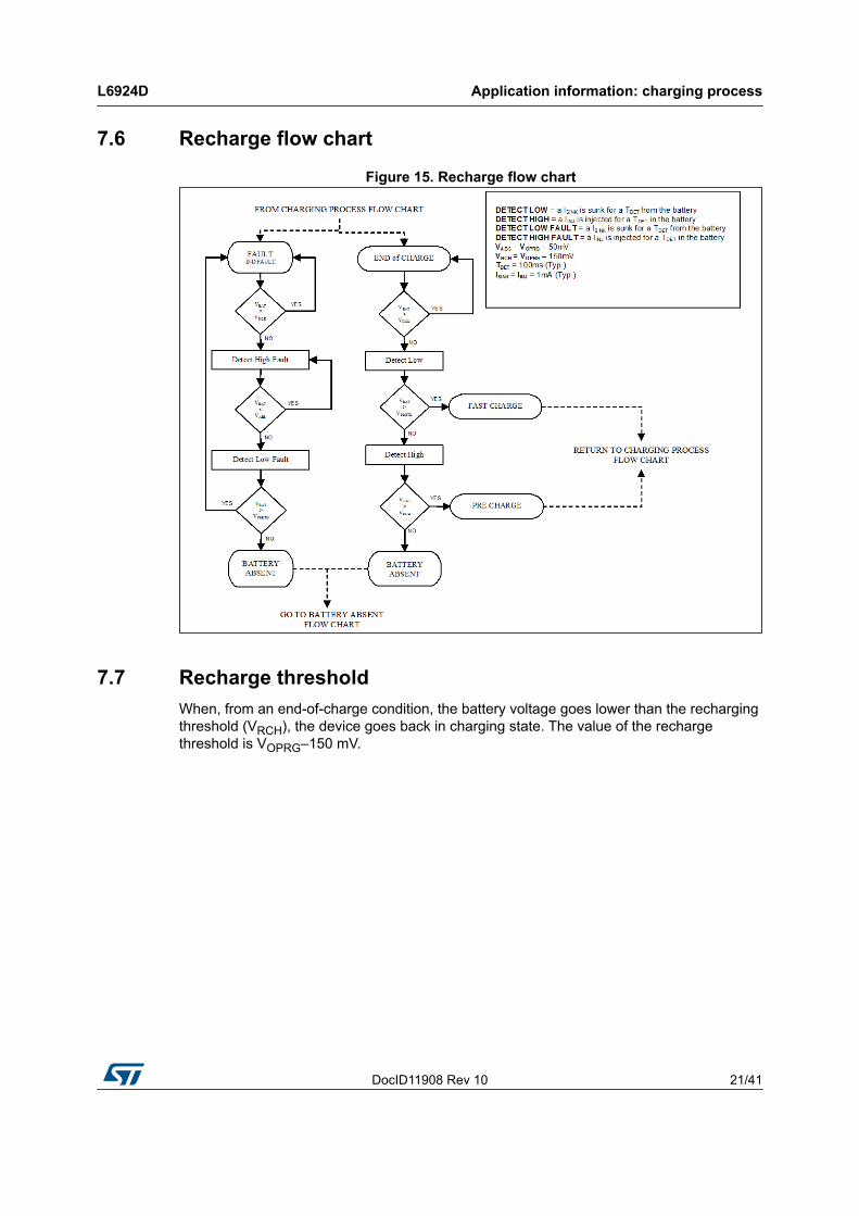
7.6 Recharge flow chart
Figure 15. Recharge flow chart
7.7 Recharge threshold When, from an end-of-charge condition, the battery voltage goes lower than the recharging threshold (VRCH), the device goes back in charging state. The value of the recharge threshold is VOPRG–150 mV.

Application information: charging process L6924D
22/41 DocID11908 Rev 10
7.8 Maximum charging timeTo avoid the charging of a dead battery for a long time, the L6924D has the possibility to set a maximum charging time starting from the beginning of the fast-charge phase. This timer can be set with a capacitor, connected between the TPRG pin and GND. The CTPRG is the external capacitor (in nF) and is given by the following equation:
Equation 11
Note: The maximum recommended CTPRG value must be less than 50 nF.
Figure 16. TPRG pin connection
Where,
VREF = 1.8V,
KT = 279 x 105,
VBG = 1.23V, and
TMAXCH is the charging time given in seconds.
If the battery does not reach the end-of-charge condition before the timer expires, a fault is issued.
Also during the pre-charge phase there is a safety timer, given by:
Equation 12
If this timer expires and the battery voltage is still lower than VPRETH, a fault signal is generated, and the charge process is terminated.
DocID11908 Rev 10 23/41
L6924D Application information: charging process
41
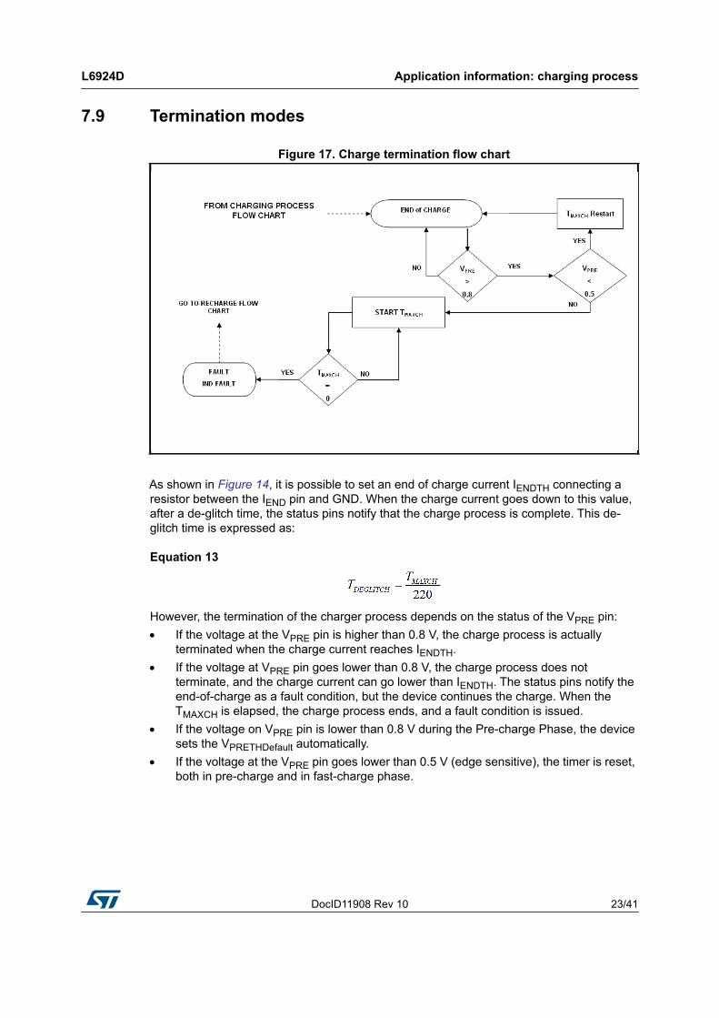
7.9 Termination modes
As shown in Figure 14, it is possible to set an end of charge current IENDTH connecting a resistor between the IEND pin and GND. When the charge current goes down to this value, after a de-glitch time, the status pins notify that the charge process is complete. This de-glitch time is expressed as:
Equation 13
However, the termination of the charger process depends on the status of the VPRE pin: If the voltage at the VPRE pin is higher than 0.8 V, the charge process is actually
terminated when the charge current reaches IENDTH. If the voltage at VPRE pin goes lower than 0.8 V, the charge process does not
terminate, and the charge current can go lower than IENDTH. The status pins notify the end-of-charge as a fault condition, but the device continues the charge. When the TMAXCH is elapsed, the charge process ends, and a fault condition is issued.
If the voltage on VPRE pin is lower than 0.8 V during the Pre-charge Phase, the device sets the VPRETHDefault automatically.
If the voltage at the VPRE pin goes lower than 0.5 V (edge sensitive), the timer is reset, both in pre-charge and in fast-charge phase.
Figure 17. Charge termination flow chart

Application information: monitoring and protection L6924D
24/41 DocID11908 Rev 10
8 Application information: monitoring and protection
The L6924D uses a VFQFPN 3 mm x 3 mm 16-pin package with an exposed pad that allows the user to have a compact application and good thermal behavior at the same time. The L6924D has a low thermal resistance because of the exposed pad (approximately 75°C/W, depending on the board characteristics). Moreover, a built-in thermal protection feature prevents the L6924D from having thermal issues typically present in a linear charger.
Thermal control is implemented with a thermal loop that reduces the charge current automatically when the junction temperature reaches approximately 120 °C. This avoids further temperature rise and keeps the junction temperature constant. This simplifies the thermal design of the application as well as protects the device against over-temperature damage.
The Figure 18 shows how the thermal loop acts (with the dotted lines), when the junction temperature reaches 120°C.
8.1 NTC thermistorThe device allows designers to monitor the battery temperature by measuring the voltage across an NTC or PTC resistor. Li-Ion batteries have a narrow range of operating temperature, usually from 0°C to 50 °C. This window is programmable by an external divider which is comprised of an NTC thermistor connected to GND and a resistor connected to VREF. When the voltage on the TH pin exceeds the minimum or maximum voltage threshold
Figure 18. Power dissipation both linear and quasi pulse mode with thermal loop

DocID11908 Rev 10 25/41
L6924D Application information: monitoring and protection
41
(internal window comparator), the device stops the charge process, and indicates a fault condition through the status pin.
When the voltage (and thus, the temperature), returns to the window range, the device re-starts the charging process. Moreover, there is a hysteresis for both the upper and lower thresholds, as shown in Figure 20.
Note: TBAT = OK when the battery temperature between 0°C and 50°C
Figure 19. Battery temperature control flow chart
Figure 20. Voltage window with hysteresis on TH

Application information: monitoring and protection L6924D
26/41 DocID11908 Rev 10
When the TH pin voltage rises and exceeds the VMINTH = 50% of VREF (900 mV typ), the L6924D stops the charge, and indicates a fault by the status pins. The device re-starts to charge the battery, only when the voltage at the TH pin goes under VMINTH_HYS = 780 mV (typ).
For what concerns the high temperature limit, when the TH pin voltage falls under the VMAXTH = 12.5% of VREF (225 mV Typ.), the L6924D stops the charge until the TH pin voltage rises to the VMAXTH_HYS = 248 mV (Typ.).
When the battery is at the low temperature limit, the TH pin voltage is 900 mV. The correct resistance ratio to set the low temperature limit at 0°C can be found with the following equation:
Equation 14
Where RUP is the pull-up resistor, VREF is equal to 1.8 V, and RNTC0°C is the value of the NTC at 0°C. Since at the low temperature limit VMINTH = 900 mV:
Equation 15
It follows that:
Equation 16
Similarly, when the battery is at the high temperature limit, the TH pin voltage is 225 mV. The correct resistance ratio to set the high temperature limit at 50°C can be found with the following equation:
Equation 17
Where RNTC50°C is the value of the NTC at 50°C. Considering VMAXTH = 225 mV it follows that:
Figure 21. Pin connection

DocID11908 Rev 10 27/41
L6924D Application information: monitoring and protection
41
Equation 18
Consequently:
Equation 19
Based on Equation 16: and Equation 19: , it derives that:
Equation 20
The temperature hysteresis can be estimated by the equation:
Equation 21
Where VTH is the pin voltage threshold on the rising edge, VTH_HYS is the pin voltage threshold on the falling edge, and NTCT (-%/°C) is the negative temperature coefficient of the NTC at temperature (T) expressed in % resistance change per °C. For NTCT values, see the characteristics of the NTC manufacturers (e.g. the 2322615 series by VISHAY). At the low temperature, the hysteresis is approximately:
Equation 22
Obviously at the high temperature hysteresis is:
Equation 23
Considering typical values for NTC0°C and NTC50°C, the hysteresis is:
Equation 24
And:
Application information: monitoring and protection L6924D
28/41 DocID11908 Rev 10
Equation 25
If a PTC connected to GND is used, the selection is the same as above, the only difference is when the battery temperature increases, the voltage on the TH pin increases, and vice versa. For applications that do not need a monitor of the battery temperature, the NTC can be replaced with a simple resistor whose value is one half of the pull-up resistor RUP.
In this case, the voltage at the TH pin is always inside the voltage window, and the charge is always enabled.
8.2 Battery absence detectionThis feature provides a battery absent detection scheme to detect the removal or the insertion of the battery. If the battery is removed, the charge current falls below the IENDTH. At the end of the de-glitch time, a detection current IDETECT, equal to 1 mA, is sunk from the output for a time of TDETECT. The device checks the voltage at the output. If it is below the VPRETH, a current equal to IDETECT is injected in the output capacitor for a TDETECT, and it is checked to see if the voltage on the output goes higher than VABS (the value is VOPRGTH-50 mV). If the battery voltage changes from VPRETH to VABS and vice versa in a TDETECT time, it means that no battery is connected to the charger. The TDETECT is expressed by:
Equation 26

DocID11908 Rev 10 29/41
L6924D Application information: monitoring and protection
41
8.3 Status pinsTo indicate various charger status conditions, there are two open-collector output pins, ST1 and ST2. These status pins can be used either to drive status LEDs, connected to an external power source, by a resistor, or to communicate to a host processor. These pins must never be connected to the VIN when it exceeds their absolute value (6 V).
Figure 22. Battery absent detection flow chart
Figure 23. ST1 and ST2 connection with LEDs or microcontroller

Application information: monitoring and protection L6924D
30/41 DocID11908 Rev 10
8.4 ShutdownThe L6924D has a shutdown pin (SD) that allows enabling or disabling the device.
If the SD pin voltage is below 0.4 V (e.g. pin connected to GND), the device is enabled, whereas if the SD pin voltage exceeds 2 V (e.g. the shutdown pin is left floating) the device is disabled.
When the device enters the shutdown mode, the current consumption is reduced to 60 μA typ. In this condition, VREF is turned off.
The Figure 24 clarifies the SD pin behavior.
Figure 24. Shutdown
Table 6. Status LEDs indicationsCharge condition Description ST1 ST2
Charge in progress When the device is in pre-charge or fast-charge status ON OFF
Charge done When the charging current goes lower than the IENDTH OFF ON
Stand by mode When the input voltage goes under VBAT-50 mV OFF OFF
Bad battery temperature When the voltage on the TH pin is out of the programmable window, in accordance with the NTC or PTC thermistor ON ON
Battery absent When the battery pack is removed ON ON
Over time When TMAXCH or TMAXPRECH is expired ON ON

DocID11908 Rev 10 31/41
L6924D Additional application information
41
9 Additional application information
9.1 Selecting the input capacitorIn most applications, a 1 μF ceramic capacitor, placed close to the VIN and VINSN pins can be used to filter the high frequency noise.
9.2 Selecting the output capacitorTypically, 1 μF ceramic capacitor placed close to the VOUT and VOUTSN pin is enough to keep voltage control loop stable. This ensures proper operation of battery absent detection in removable battery pack applications.

Additional application information L6924D
32/41 DocID11908 Rev 10
9.3 Battery floating voltage setupThe L6924D has been evaluated with the following application schematic.
Figure 25. L6924D application schematic
Table 7. External component values for the L6924DName Value Description Note
R1, R2 1 kΩ Pull-up resistor
C1 1 μF Input supply voltage capacitor
C2 10 nF Maximum charging time capacitor
Rosns 7500 Ω VFLOAT programming resistor
C3 1 μF Output battery capacitor
R3 1 kΩ NTC supply resistor
R9 470 Ω NTC tuning parallel resistor
C4 1 μF VREF filter capacitor
R6 Not populated Pre-charge voltage programming resistorVPRE = 2.8 V as default value
R10 Not populated Pre-charge voltage programming resistor
R5 48.6 kΩ Fast-charge current programming resistor IFAST = 240 mA
R4 2.2 kΩ Set standard IEND = 10% IFAST IEND ~ 24 mA
R7 Not populated Pre-charge current default 10%IPRE ~ 24 mA as default value
R8 Not populated Pre-charge current default 10%

DocID11908 Rev 10 33/41
L6924D Additional application information
41
9.3.1 Battery floating voltage: VFLOAT
The battery floating voltage can be set to a value higher than 4.2 V by using the following formula:
VFLOAT = 4.2 V + Rosns * 19.5 μA = 4.346 V
As an example, with Rosns = 7.5 kΩ the battery floating voltage (VFLOAT) is set to be VFLOAT = 4.346 V.
Figure 26. VFLOAT vs. Rosns
The L6924D works with the selected external components. The test results confirm that their behavior is in line with the design.
9.4 Layout guidelines and demonstration board descriptionThe thermal loop keeps the device at a constant temperature of approximately 120°C which in turn, reduces ICHG. However, in order to maximize the current capability, it is important to ensure a good thermal path. Therefore, the exposed pad must be properly soldered to the board and connected to the other layer through thermal vias. The recommended copper thickness of the layers is 70 μm or more.
The exposed pad must be electrically connected to GND. Figure 27 shows the thermal image of the board with the power dissipation of 1 W. In this instance, the temperature of the case is 89°C, but the junction temperature of the device is given by the following equation:
Equation 27
Where the RTH J-A of the device mounted on board is 75 °C/W, the power dissipated is 1 W, and the ambient temperature is 25 °C.

Additional application information L6924D
34/41 DocID11908 Rev 10
In this case the junction temperature is:
Equation 28
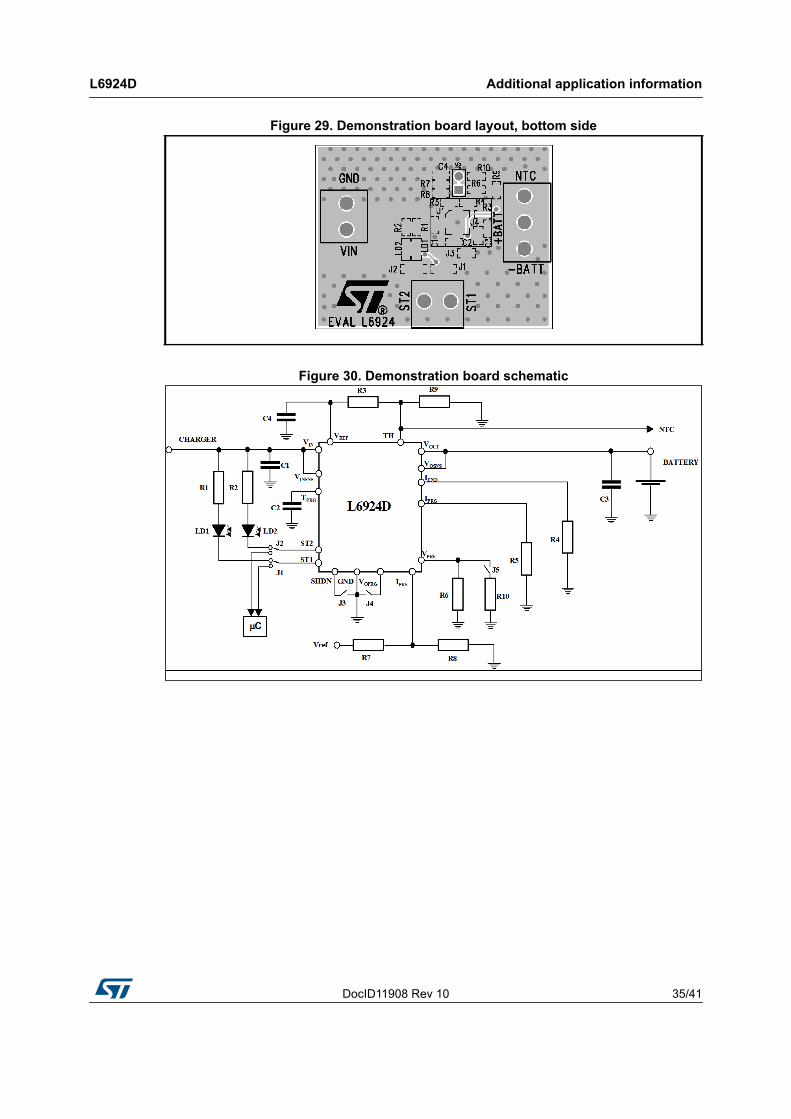
The VOSNS pin can be used as a remote sense; it should be therefore connected as closely as possible to the battery. The demonstration board layout and schematic are shown in Figure 28, Figure 29 and Figure 30.
Figure 27. Thermal image of the demonstration board
Figure 28. Demonstration board layout, top side
DocID11908 Rev 10 35/41
L6924D Additional application information
41
Figure 30. Demonstration board schematic
Figure 29. Demonstration board layout, bottom side

Additional application information L6924D
36/41 DocID11908 Rev 10
Table 8. Demonstration board components descriptionName Value Description
R1 1k Pull up resistor. To be used when the ST1 is connected to a LED.
R2 1k Pull up resistor. To be used when the ST1 is connected to a LED.
R3 1k Pull up resistor. Connected between VREF and TH pin.
R4 3k3 End of charge current resistor. Used to set the termination current and, as a “Gas Gauge” when measuring the voltage across on it.
R5 24k Fast-charge current resistor. Used to set the charging current.
R6 N.M. VPRETH resistor. Used to set programmable pre-charge voltage threshold. If not mounted, the VPRETHDefault, equal to 2.8V, is set.
R7 N.M. IPRETH resistor. Used to set the programmable pre-charge current threshold below the default one. If not mounted, the IPRETHDefault is set.
R8 68k IPRETH resistor. Used to set the programmable pre-charge current threshold above the default one. If not mounted, the IPRETHDefault is set.
R9 470R If a NTC is not used, a half value of R3 must be mounted to keep the TH voltage in the correct window.
R10 N.M. It has the same function of R6. Moreover, if it is replaced with a short-circuit, when J5 is closed, the timer is reset (falling edge).
C1 1μF Input capacitor.
C2 10nF TMAX capacitor. Used to set the maximum charging time.
C3 4.7μF Output capacitor.
C4 1nF VREF filter capacitor.
LD1 GREEN ST1 LED.
LD2 RED ST2 LED.
J1 ST1 jumper. Using to select the LED or the external μC.
J2 ST2 jumper. Using to select the LED or the external μC.
J3 SD jumper. If open, the device is in shutdown mode; when closed, the device starts to work.
J4 VOPRG jumper. If closed, the 4.2V output voltage is set; if open, the 4.1V is set.
J5 VPRE jumper. If closed with R10 in short-circuit with GND, resets the timer.

DocID11908 Rev 10 37/41
L6924D Application ideas
41
10 Application ideas
10.1 USB battery chargerWith a voltage range between 4.75 V and 5.25 V, and a maximum current up to 500 mA, the USB power bus is an ideal source for charging a single-cell Li-Ion battery. Since it is not possible to rely on the USB current limit to charge the battery, a linear approach must be adopted. Therefore, it is only necessary to set the ICHG with a maximum value lower than 500 mA, and the device will charge the battery in Linear mode.
Figure 31 shows an example of USB charger application schematic.
Figure 31. USB charger application

Package information L6924D
38/41 DocID11908 Rev 10
11 Package information
In order to meet environmental requirements, ST offers these devices in different grades of ECOPACK® packages, depending on their level of environmental compliance. ECOPACK® specifications, grade definitions and product status are available at: www.st.com. ECOPACK® is an ST trademark.

DocID11908 Rev 10 39/41
L6924D Package information
41
11.1 VFQFPN16 package information
Table 9. VFQFPN16 (3 x 3 mm) mechanical data
Dim.mm.
Min. Typ. Max.
A 0.80 0.90 1.00 A1 0.02 0.05 A2 0.65 1.00 A3 0.20 b 0.18 0.25 0.30 D 2.85 3.00 3.15 D2 1.45 1.60 1.75 E 2.85 3.00 3.15 E2 1.45 1.60 1.75 e 0.45 0.50 0.55 L 0.30 0.40 0.50
Figure 32. VFQFPN16 (3 x 3 mm) mechanical drawing
7185330_G

Revision history L6924D
40/41 DocID11908 Rev 10
12 Revision history
Table 10. Document revision historyDate Revision Changes
16-Dec-2005 1 First draft
20-Dec-2005 2 Package dimensions updated
10-Jan-2006 3 Few updates
14-Feb-2006 4 Part number updated
03-Jul-2006 5 Updates to equation in page 22, updated block diagram Figure 4.
07-Sep-2006 6 Added Note: on page 22, updated value CTPRG page 8
29-Jun-2007 7 Updated capacitor values C2, C3 in Table 8 on page 36
05-Jul-2010 8 Updated Table 5 on page 8 and Section 8.4 on page 30
22-Sep-2010 9 Updated Table 9 and Figure 32 on page 39. Minor changes.
25-Sep-2017 10Updated Applications and Table 1: Device summaryUpdated power dissipation in Table 4: Thermal dataAdded Section 9.3: Battery floating voltage setup

DocID11908 Rev 10 41/41
L6924D
41
IMPORTANT NOTICE – PLEASE READ CAREFULLY
STMicroelectronics NV and its subsidiaries (“ST”) reserve the right to make changes, corrections, enhancements, modifications, and improvements to ST products and/or to this document at any time without notice. Purchasers should obtain the latest relevant information on ST products before placing orders. ST products are sold pursuant to ST’s terms and conditions of sale in place at the time of order acknowledgement.
Purchasers are solely responsible for the choice, selection, and use of ST products and ST assumes no liability for application assistance or the design of Purchasers’ products.
No license, express or implied, to any intellectual property right is granted by ST herein.
Resale of ST products with provisions different from the information set forth herein shall void any warranty granted by ST for such product.
ST and the ST logo are trademarks of ST. All other product or service names are the property of their respective owners.
Information in this document supersedes and replaces information previously supplied in any prior versions of this document.
© 2017 STMicroelectronics – All rights reserved