appendix a: 8085 instruction set by opcode - springer978-1-349-06978-1/1.pdf · appendix a: 223...
TRANSCRIPT

Appendix A:
223
8085 InstructionSet by Opcode
The information in this appendix is reproduced by kind permission of the IntelCorporation. The symbols and abbreviations used are listed below .
Symbol
AB,C,DE,H,LFMbytedbIeaddrportr, rl, r2rp
PCCYPACZS
Meaning
Accumulator
} One of the internal registers
Represents the flag registerThe 16-bit memory address currently held by the register pair Hand LAn 8-bit data quantityA 16-bit (two byte) data quantityA 16-bit addressAn 8-bit I/O port addressOne of the registers A, B, C, D, E, H, LOne of the following register pairs
B represents the register pair Band CD represents the register pair D and EH represents the register pair Hand LPSW represents the register pair A and FSP represents the 16-bit stack pointer
The 16-bit program counterCarry flagParity flagAuxiliary carry flagZero flagSign flag

224 Microelectronics and Microprocessor-based Systems
Data Transfer Group
These instructions transfer data between registers and memory.Flags - none affected by instructions in this group.
Move
A,A 7F B,A 47 C,A 4FA,B 78 B,B 40 C,B 48A,C 79 B,C 41 C,C 49
MaVA,D 7A
MaVB,D 42
MaVC,D 4A
A,E 7B B,E 43 C,E 4BA,H 7C B,H 44 C,H 4CA,L 7D B,L 45 C,L 4DA,M 7E B,M 46 C,M 4E
D,A 57 E,A SF H,A 67D,B 50 E,B 58 H,B 60D,C 51 E,C 59 H,C 61
MaVD,D 52
MaVE,D SA
MaVH,D 62
D,E 53 E,E 5B H,E 63D,H 54 E,H 5C H,H 64D,L 55 E,L 5D H,L 65D,M 56 E,M 5E H,M 66
Move Immediate
L,A 6F M,A 77 A,byte 3EL,B 68 M,B 70 B,byte 06L,C 69 M,C 71 C,byte OE
MaVL,D 6A
MaVM,D 72
MYID,byte 16
L,E 6B M,E 73 E,byte IEL,H 6C M,H 74 H,byte 26L,L 6D M,L 75 L,byte 2EL,M 6E M,byte 36
Load Immediate (Reg. pair) Load/Store A direct
{ B,db!, 01 LDAXB OA
LXID,dble 11 LDAXD lAH,dble 21 STAXB 02SP,dble 31 STAXD 12
Load/Store A direct Load/Store HL direct
LDA addr 3A LHLD addr 2ASTA addr 32 SHLDaddr 22

Appendix A : 8085 Instruction Set by Opcode 225
Exchange HL with DE
XCHG EB
Data Manipulation Group - Arithmetic
Instructions in this group perform arithmetic operations on data in the registers andthe memory.
Add*
A 87 A 8FB 80 B 88C 81 C 89
ADDD 82
ADCD 8A
E 83 E 8BH 84 H 8CL 85 L 8DM 86 M 8E
Subtract*
A 97 A 9FB 90 B 98C 91 C 99
SUBD 92
SBBD 9A
E 93 E 9BH 94 H 9CL 95 L 9DM 96 M 9E
Add/Subtract Immediate* Double Length Add***
ADI byte C6
DAD {~09
ACI byte CE 19SUI byte D6 29SBI byte DE SP 39
Increment/Decrement**
A 3C A 3DB 04 B 05C OC C OD
INRD 14
DCRD 15
E lC E 10H 24 H 25L 2C L 2DM 34 M 35

226 Microelectronics and Microprocessor-based Systems
Increment/Decrement Register Pair****
U03
HpOB
INX13
DCXIB
23 2B33 3B
Complement AU**Decimal Adjust A*
DAA 27 CMA 2F
Complement/Set CY***
CMC 3FSTC 37
Arithmetic Immediate*
AD! byte C6ACI byte CESUI byte D6SBI byte DE
Notes* All flags may be affected.** All flags except CARRY may be affected.*** Only CARRY FLAG affected.**** No flags affected.
Data Manipulation Group - Logical
Instructions in this group perform logical operations on data in the registers and thememo ry.
AND* OR* Exclusive-OR*
A A7 A B7 A AFB AO B BO B A8C Al C Bl C A9
ANAD A2
ORAD B2
XRAD AA
E A3 E B3 E ABH A4 H B4 H ACL AS L B5 L ADM A6 M B6 M AE

Appendix A : 8085 Instruction Set by Opcode 227
CMP
Compare*
ABCDEHLM
BFB8B9BABBBCBDBE
Rotate***
RLC 07RRC OFRAL 17RAR IF
Logical Immediate*
ANI byte E6XRI byte EEORI byte F6CPI byte FE
Notes* All flags may be affected .*** Only the CARRY flag may be affected.
Transfer of Control Group or Branch Group
This group of instructions alters the sequence of program flow by testing th econdition flags.
Jump Call Return
IMP addr C3 CALL addr CD RET C9INZ addr C2 CNZ addr C4 RNZ COIZ addr CA CZ addr CC RZ C8INC addr D2 CNC addr D4 RNC DOIC addr DA CC addr DC RC D8IPO addr E2 CPO addr E4 RPO EOJPE addr EA CPE addr EC RPE E8IP addr F2 CP addr F4 RP FO1M addr FA CM addr FC RM F8
Jump Indirect
PCHL E9
Input/Output Group
This group of instructions performs I/O instructions between the accumulator and aspecified port.IN port DBOUT port D3

228 Microelectronics and Microprocessor-based Systems
Stack and Machine Control Group
This group ofinstruc tions maintains the stack and internal control flags.
Stack operations
{LC5
{LCI
PUSHD5
POPD1
E5 EIF5 FI
XTHL E3 SPHL F9
Interrupt Control Processor Control
EI FB NOP 00DI F3 HLT 76RIM 20SIM 30
Restart
0 C71 CF2 D7
RST3 DF4 E75 EF6 F77 FF

Appendix B:
229
8085 InstructionSet by ClockCycles
STACK OPERATIONSPUSH B 12PUSH D 12PUSH H 12PUSH PSW 12POP B 10POP D 10POP H 10POPPSW 10XTHL 16SPHL 6
MOVE, LOAD AND STOREMOV rl,r2 4MOVM,r 7MOVr,M 7MVI r 7MVI M 10LXI B 10LXID 10LXI H 10LXI SP 10STAXB 7STAXD 7LDAX B 7LDAX D 7STA 13LDA 13SHLD 16LHLD 16XCHG 4
Mnemonic Clock cycles Mnemonic Clock cycles
RETURNRET 10RC 6/12RNC 6/12RZ 6/12RNZ 6/12RP 6/12RM 6/12RPE 6/12RPO 6/12
RESTARTRST 12
INPUT/OUTPUTIN 10OUT 10
INCREMENT AND DECREMENTINRr 4DCRr 4INR M 10DCRM 10INXB 6INXD 6INXH 6INX SP 6DCXB 6DCXD 6DCXH 6DCX SP 6

230 Microelectronics and Microprocessor-based Systems
JUMP ADD1MP 10 ADDr 41C 7/10 ADCr 41NC 7/10 ADDM 71Z 7/10 ADCM 71NZ 7/10 ADI 71P 7/10 ACI 71M 7/10 DADB 101PE 7/10 DADD 101PO 7/10 DADH 10PCHL 6 DADSP 10
CALL SUBTRACTCALL 18 SUB r 4CC 9/18 SBB r 4CNC 9/18 SUBM 7CZ 9/18 SBBM 7CNZ 9/18 SUI 7CP 9/1 8 SBI 7CM 9/18CPE 9/18 LOGICALCPO 9/18 ANAr 4
XRAr 4ROTATE ORAr 4RLC 4 CMP r 4RRC 4 ANAM 7RAL 4 XRA M 7RAR 4 ORAM 7
CMP M 7SPECIALS ANI 7CMA 4 XRI 7STC 4 ORI 7CMC 4 CPI 7DAA 4
INTERRUPTMASKCONTROL RIM 4EI 4 SIM 4DI 4NOP 4HLT 5
No te: Two possible cycle times, for example, 6/12, indicates that the number ofinstruction cycles involved is dependent on the condition flags.

231
Solutions to Problems
l.l (a) 354 8 , (b) 0111011002 , (c) OECH.1.2 (a) 111011 2 , (b) 153l 8,(c) 1245H.1.3 (a) 2730 , (b) 156, (c) 85.1.4 (a) 10001000010002 , (b) 104108 , (c) 1108H.1.5 (a) - 86, (b) - 85.1.6 (a) 00000101 , (b) 111110ll ,(c) Ill00110,(d) 10110000.1.7 (a) 65 535 , (b) +32767 and - 32 768.1.8 Both the carry and overflow flags are 'set' to ' 1'.
2.9 4K locations.2.11 ROM A = ROM B = tK.
RAM C =RAM D =RAM E =RAM F =tK.System expansion blocks = lK each.
5.5 (a) 2K, (b) (i) OOOOH, (b) (ii) 07FFH.5.6 (a) F800H, (b) FFFFH.
7.2 219 100rDBH.
7.3 3.28 ms.
9.15 MVI H,OOMVI L,byteLXI D,2000HDADDMOV A,MSTA 200FHHLT
; HIGH BYTE OF INDEX ADDRESS =OOH; LOWBYTE OF INDEX ADDRESS IN L; BASE ADDRESS OF TABLE IN D AND E; FORM EFFECTIVE ADDRESS OF RESULT; GET PETHERICK CODE FROM TABLE; STORE IT IN 200FH; HALT
10.4 COUNT 1 = 219 10 or DBH, COUNT 2 = 199 10 or C7H.(Note: in general the value of the product COUNT 1 x COUNT 2 =43 581 10 ,)
11.7 (a)PC 2060SP 20AE
(b)208020AC
(c) (d)20AO 208C20AA 20AC
(e)206820AE
(f)202520BO

232 Microelectronics and Microprocessor-based Systems
12.3Address Byte Label Instruction Comment
mnemonicI 2 3
2010 3EOl MYI A,OlH2012 D3 20 OUT20H ; INITIALISE PIO2014 31 BO 20 LXI SP,20BOH ; INITIALISE STACK POINTER20 17 DB 22 IN 20H ; READ SWITCHES20 19 2F CMA ; COMPLEMENT DATA20 l A 3200 20 LOOP: STA 2000H ; STORE DATA IN 2000H20 ID D3 21 OUT 21H ; DISPLAY DATA ON LEDs20 l F CD 09 03 CALL TIME ; CALL TIME DELAY2022 DBn IN22H ; READ SWITCHES2024 A7 ANA A ; SET FLAGS2025 C2 IA 20 JNZ LOOP ; RETURN TO LOOP IF ANY
; SWITCH = I202 8 D3 21 OUT 21H ; EXTINGUISH LEDS202A 76 HLT ; HALT PROGRAM
12.4
Label
START:
Instructionmnemonic
LXI SP,20BOHMYI A,OIHOUT 20HIN 22HSTA 2000H
CALL 03DFHLDA 2000HXRIOFHOUT 21HJMPSTART
Comment
; INITIALISE STACK POINTER; INITIALISE PIO
; READ STATE OF SWITCHES; STORE DATA IN LOCATION
2000H; DISPLAY DATA ON YDU; RECALL DATA; INVERT LOW BYTE OF DATA; DISPLAY RESULT ON LEDS; READ SWITCHES ONCE AGAIN
14.5 0010H, 00 20H , 00 24H , 003CH.14.6 Yes.14.8 LXI SP,20BOH ; INITIALISE STACK POINTER
MYI A,OCH ; UNMASK RST 6.5 AND 5.5SIMEI ; ENABLE INTERRUPTS

Solutions to Problems
14.9
233
Address Byte
1 2 3
Label Instructionmnemonic
Comment
2020 06042022 21 00202025 972026 862027 232028 052029 C2 26 20202C 320420202F 762030 C3 3020
MVI B,04H ; LOAD COUNTERLXI H,2000H ; POINTER M = 2000HSUB A ; CLEAR ACCUMULATOR
LOOP: ADD M ; FORM SUM IN ACCUMULATORINX H ; INCREMENT POINTEROCR B ; DECREMENT COUNTERJNZ LOOP ; JUMP IF SUM NOT COMPLETESTA 2004H ; STORE SUMHLT ; WAIT FOR INTERRUPT
STOP: JMP STOP ; TERMINATE PROGRAM
2080 3A 04202083 072084 072085 E6 FC2087 320520
208B C9
INTR: LDA 2004HRLCRLCANIFCSTA 2005H
RET
; GET SUM; ROTATE DATA LEFT TWICE; TO MULTIPLY BY FOUR; MASK OUT NON-SIGNIFICANT BITS; STORE PRODUCT; INTERRUPT NEED NOT BE RE
ENABLED; RETURN TO MAIN PROGRAM
14.10 (a) 5.325 ms (b) 21.3 ms.
234
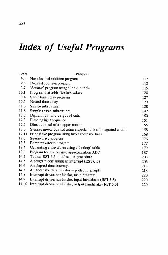
Index of Useful Programs
Table9.49.59.7
10.110.410.511.611.812.212.312.512.612.1113.213.313.413.614.214.314.614.714.814.914.10
ProgramHexadecimal addition programDecimal addition program'Squares' program using a lookup tableProgram that adds five hex valuesShort time delay programNested time delaySimple subroutineSimple nested subroutinesDigital input and output of dataFlashing light sequenceDirect control of a stepper motorStepper motor control using a special 'driver' integrated circuitHandshake program using two handshake linesSquare wave programRamp waveform programGenerating a waveform using a 'lookup' tableProgram for a successive approximation ADCTypical RST 6.5 initialisation procedureA program containing an interrupt (RST 6.5)An elapsed time interruptA handshake data transfer - polled interruptsInterrupt-driven handshake, main programInterrupt-driven handshake , input handshake (RST 5.5)Interrupt-driven handshake, output handshake (RST 6.5)
112113115120127129138142150151155158168176177179187203206213218220220220

Index
Accumulator 28Accumulator I/O addressing 24Addition 6
binary 7double-length 88hexadecimal 8
Address 18Address bus I 8Address decoding 45-58Address field IIIAddress/data bus 32Addressing mode 102
direct 105extended 105immediate 102implied 104indexed 106, 114indirect 106inherent 104register direct 106register indirect 107relative 109stack 106zero page 106
Algorithm 82Analogue-to-digital convertor (ADC)
179continuous balance 182interfacing to 188-94successive-approximation 183-8
Architecture of CPU 28Arithmetic and logic instructions 96Arithmetic and logic unit (ALU) 14, 30Arithmetic shift 100Assem bier statement 110Assembly language 94, 110Auxiliary carry flag 30
235
Base IBaud rate 74Bidirectional data bus 18Binary digit (bit) 2Binary number IBit time 74Branch instructions see Jump
instructionsBreak point 93Buffer 60Bus system 18, 26Byte 12
Call instruction 132Carry flag 9, 29 , 30
auxiliary 30Central processing unit (CPU) 14Chip ISChip enable pin 20 ,25Chip select pin 20, 46 , 47Clock oscillator 16, 31, 35Code conversion 116Comment , in program IIIComparison instruction 98Complement, binary 9Conditional call instructions 132Conditional jump instructions 101Conditional return instructions 132Control and timing section 31Control bus 18Control unit of CPU 14CIS register of PIO 147
command aspect of 147,148 ,164
status aspect of 166

236
Data bus 18Data manipulation instructions 95Data rate 76Data transfer instructions 95Debugging 90Decimal adjustment instruction 112 ,
113Decoder 46-57Dedicated microcomputer 14Delay (time) routine 78-80 , 125-9Device enable pin 20Device select pin 20Digital computer 14Digital input and output 148Digital-to-analogue convertor (DAC)
173-9waveform generation using 175
Direct digital control (DDC) 152Displacement 108Dual-in-line package (DIP) ISDynamic RAM 44
Effe ctive address 108 , 114EPROM 16, 17
Fetch--execute cycle 33Field structure , of assembly language
instruction 110-13FIFO store 44Firmware 18Flag 9 ,29Flag register 9 , 29Flip-flop 9Flowchart 82Foldback, on memory map 57Full-adder 7
General-purpose computer 14
Half-carry flag see Auxiliary carry flagHandshake 42 , 159-69
implementing 161input 160 ,163output 160 , 163
Hardware 17Hexadecimal numbers 3
Index (in addressing mode) 114Index register 108Input/output port 17,20, 23
bidirectional 22dedicated 17programmable 17, 145-8unidirectional 22
Instruction decoder 3 1Instruction register 30Instruction set 94,223,229Integrated circuit ISInterface 17, 60Interrupt 41 , 196
handshake 214-21maskable 196multilevel 206non-maskable 41 , 196polled 197 , 217priority of 200timer (PIO) 209vectored 197 , 1998085 198
Interrupt flag 197Interrupt handling 202Interrupt mask (I register) 200Interrupt routine 41Interval timer 78I/O control module 148, 149I/O read 39I/O timing 39I/O write 37
Jump instructions 101
Keyboard 67-73
Label , in program 86 ,94, IIILatched I/O port 63-7 ,70LED ,7-segment 63-8LIFO store 44 , 106 , 134Listener, in handshake 160
Index

Index
Logical instructions 96-100Logical shift 100Lookuptable 113-16,178 ,179Loop, in program 118
Machine code instruction 94,95,109Machine cycle 35Mainframe computer 14Maskable interrupt 196Memory 14Memory access time 39Memory map 23Memory read 38Memory register 28Memory write 36Memory-mapped address 24Memory-mapped I/O 24Microcomputer 14Microcycle 35Microprocessor-based system 14, 18
minimal 17Minicomputer 14Monitor program 92Multiplexing 32
Negative flag 30Negative number, binary 9, 10Non-maskable interrupt 41 , 196Non-volatile memory 44Number conversion 4-6
Octal number 2Offset 108, 114One's complement 9, 10Opcode 30 ,90, IIIOperand 14Operand field , in assembly program
IIIOperation code 30,90Output port 20-3Overflow 12Overflow flag 12
23 7
Page 23Parallel I/O port 20-3Parameter passing 143Parity flag 29 ,30Peripheral 17Pointer register 28 ,105Polling 40, 217POP instruction 135-7Port 17,20,33,145Processor status word (PSW) 137Program 14, 17,82Program counter 28Programmable I/O port 17, 145-8
timer in 209Programmable timer 80Pseudo-operation 112PUSH instruction 135-7
Radix 1RAM (random-access memory) 16,44Read signal 31Read-write memory 16Real-time clock 78Register 28Return instruction 132Rollover (keyboard) protection 70ROM (read-only memory) 16,47Rotate instruction 98
Serial I/O port 20 ,23,73Seven-segment display 63-8Sign bit 9Sign flag 30Signed binary num ber 9Single stepping 93Software 17Stack 134Stack pointer 29, 135State, timing 35Static RAM 44Status register see Flag registerStepper motor 152-9Store 14Strobed data transfer 159Structured programming 82-7

23 8
Subroutine 132 ,149nested 140
Subroutine call 102Subroutine return 102Subroutine structure 133Subtraction, binary 10, 11Successive-approximation ADC 183-8Symbolic address (lab el) 86 ,94
Talker, in handshake 159Test and bran ch instructions 101Three-stat e (tri-state) gate 24-6 ,60Time delay program 78-80 ,125-7,
151nested I 27-9
Timer (PIO or hardware) 209Timing sequences 78Tra ce rou tine 90
Index
Trace table 89 ,92 ,139T-state 35Two's complement 10, II
UART 73Unconditional jump instruction 101Unsigned binary number 8 , 11
Vectored interrupt 197 ,199Video display unit (V DU) 18Volatile memory 44
Write signal 31
Zero flag 30