andrés cantarero university of valencia spain. valence band composing one of the most important...
TRANSCRIPT

OPTICAL PROPERTIES OF III-N NANOSTRUCTURES
Andrés CantareroUniversity of ValenciaSpain
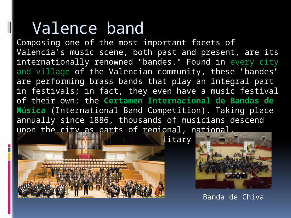
Valence bandComposing one of the most important facets of Valencia's music scene, both past and present, are its internationally renowned "bandes." Found in every city and village of the Valencian community, these "bandes" are performing brass bands that play an integral part in festivals; in fact, they even have a music festival of their own: the Certamen Internacional de Bandas de Música (International Band Competition). Taking place annually since 1886, thousands of musicians descend upon the city as parts of regional, national, international, civilian and military brass bands.
Banda de Chiva

Valencia and its University Valencia, 138 bce
810,000 p;1,500,000 mr
The University was founded in 1499
We have 45,000 students

Outline
Interest in nitride semiconductors: applications
Generalities on III-N semiconductors GaN/AlN self-assembled quantum dots
Growth of GaN/AlN/SiC self-assembled QDs Optical properties of polar and non polar QDs
Q1D semiconductor nanostructures InN nanowires
Growth of InN nanowires Optical properties of InN nanowires
Conclusions

Optical storage devices
1985 1990 1995 2000 2005 20100
200
400
600
800
1000
CD DVD HD/BD VD NG-VD
Inst
alle
d (
10
00
00
0)
Year
World database on installed optical memories
Sony launches its Blue-ray recorder (Sept 20th, 2006)
54 Gb capacity
400 nm laser (Nichia Corp)
Prof. Nakamura (UCSB) fabricated a 443.9 nm laser based on NP InGaN/GaN

White LEDs
Kittilä (Finland) , 2.2.2009
1st prize street (ecological) illumination Fallas 2009
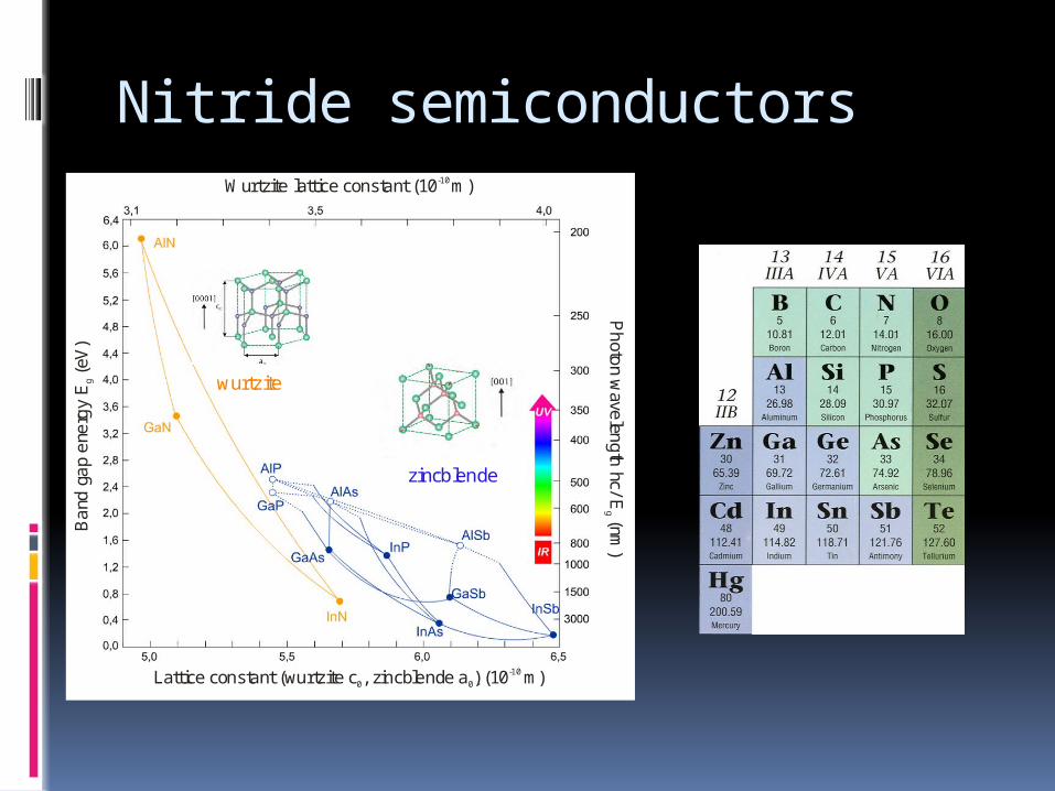
Nitride semiconductors
wurtzite
zincblende
Lattice constant (wurtzite c , zincblende a ) 0 0 (10 m)-10
Ba
nd g
ap
ene
rgy
E g(
eV)
Ph
oton w
avelen
gth
hc/ E g (nm
)
Wurtzite lattice constant (10 m)-10

Crystal structure
GaN crystallizes in the wurtzite structure under normal conditions
Difference of packing between wurtzite and ZB
Origin of PSP in Ga-face GaN

Structural parameters and PSP
F. Bernardini, V. Fiorentini, D. Vanderbilt, PRB 56, R10024 (1997).
But, it is grown on Al2O3, SiC or Si(111)
There is, additionally, PPZ
1010 disl/cm2

Growth of GaN/AlN QDs
AlN
6H-SiC
Ga + NGa
Modified Stranski-Krastanow mode
Elastic relaxation
GaNdot
AlN
AlN [0001]
[2-1-10]
2nm
GaNdot
AlN
AlN [0001]
[2-1-10]
2nm
C. Adelmann et al APL 81, 3064 (2002); N. Gogneau et al JAP 94, 2254 (2003)

PL and electric field
1 10 100
200
400
600
800
1.5 2.0 2.5 3.0 3.5 4.0 4.5 5.0
0.0
0.2
0.4
0.6
0.8
1.0
FW
HM
(m
eV)
GaN Periods
3 periods 10 periods 50 periods 200 periods
Norm
alize
d P
L
Energy (eV)
Photoluminescence of different samples growth with different number of periods
0.5 1.0 1.5 2.0 2.5 3.0
2.0
2.5
3.0
3.5
4.0
4.5
5.0
2 4 6 8 10 12
Ref a Ref b Ref c Ref d Ref e
PL
Em
issi
on
En
erg
y (
eV
)d
QW (nm)
Absorption Emission
Stokesshift
GaN Bulk
dQW
(ML)
(0001) GaN/AlN QWs
F=10 MV/cm
(a): J. M. Llorens, PhD (2006), Univ. Valencia; (b) Salviati et al., J. Phys. Cond. Matt. 16, S115 (2004); (c) Miyamura et al., APL 80 3937 (2002); (d) Kako et al., APL 83, 984 (2003); (e) Widmann et al., APL 83, 7619 (1998).
The built in electric field manifests in the optical properties of GaN/AlN heterostructures through the Stark effectIs there a way to reduce dislocations and Stark effect?

Non polar QDs5 nm
[1-100]
[0001]
HRTEM
AFM
S. Founta et al, APL 86, 171901 (2005)
a- and m-plane contain the same amount of Ga and N per layer
2,0 2,2 2,4 2,6 2,8 3,0 3,4 3,6 3,8 4,0
a-plane QDsc-plane QDsRT
Inte
nsity
(arb
. uni
ts)
Energy (eV)
100 Wcm-2
10 Wcm-2
1 Wcm-2
N. Garro et al., APL 87, 011101 (2005)
[0001]Plano a
[1120]
2.0 2.2 2.4 2.6 2.8 3.0 3.4 3.6 3.8 4.0 4.2
a-plane QDsc-plane QDs
RT
1 Wcm-2
Inte
nsit
y (a
rb. u
nits
)
Energy (eV)
GaN Laser

V and electric field
A-plane QD
Z
X
X
Z
C-plane QD
-20 -15 -10 -5 0 5 10 15 20
-0,4
-0,2
0,0
0,2
0,4
-6 -4 -2 0 2 4 6 8
-1,0
-0,5
0,0
0,5
1,0
-8
-6
-4
-2
0
2
4
-0,5
0,0
0,5
1,0
Pot
entia
l (V
)
Z (nm)
Ele
ctric
Fie
ld (
MV
/cm
)
Pot
entia
l (V
)
Z (nm)
piezo
spont
tot
Ele
ctric
Fie
ld (
MV
/cm
)
Etot

Growing interest in SNWs
1990
1992
1994
1996
1998
2000
2002
2004
2006
2008
0
1000
2000
3000
4000
5000
6000
7000
8000
1996
1997
1998
1999
2000
2001
2002
2003
2004
2005
2006
2007
2008
2009
0
20000
40000
60000
80000
100000
120000
140000
Published papers on semiconductor NWs (Web of Sciences)
Comparison of the number of citations on QDs and NWs
•Quasi-one dimensional symmetry•Large surface/volume ratio•New possible heterostructures•High quality materials (strain free)•High quality heterointerfaces (larger LM)

From QWs to NWs
Thanks to Bruno Daudin, CEA Grenoble
Ingredients:-lattice mismatch -(2.5 % Da/a GaN on AlN)- surface energy (Ga bilayer)
AlNGaN
N-rich conditions
Ga bilayer conditions
GaN grown on AlN
Fixed N flux

Self-organized growth of InN NWs

Growth details
SampleTs (ºC)
In-BEP (10-8 mbar)
N2 Flux (sccm)
G053 400 3.0 2.0
G071 475 3.0 2.0
G047 500 3.0 2.0
G044 500 3.0 1.5
G041 500 1.5 1.5
Two sets of samples:
Set A: Different substrate temperature.
Set B: Different In-BEP and N2 flux conditions.
InN nanocolumns growth: • Grown by plasma-assisted MBE. • p-Si (111) substrate.• Growth time of 300 minutes.• N2 rich conditions.
Ts: Substrate temperature.In-BEP: Base equivalent pressure of In.
J. Segura et al, ICNS7 (Las Vegas), 2007.

Raman modes of the wurtzite structure
546 (TO)732 (LO)
555 (TO) 741 (LO)
137 592 cm-1
447 (TO)585.4 (LO)
476 (TO) 593 (LO) 87 490.1 cm-1InN
GaNWurtzite : hexagonal structure with 4 atoms in the unit cell.
A 1 E 1 B 1l B 1h E 2l E 2h
G=2A1+2B1+2E1+2E

Raman scattering results
420 440 460 480 500 580 600
0.0
0.4
0.8
1.2
(x2)
Eh
2 G041 G053
Inte
nsi
ty (
arb
. u
nits
)
Raman shift (cm-1)
E1(LO)
A1(LO)
E1(TO)
PLP-
A1(TO)
Very narrow E2h non polar mode
peak, an indication of the high crystalline quality
Forbidden modes
Lower plasmon-LO coupled (PLP-) mode is observed
Sample E2h* FWHM (E2h)
E1(LO) FWHM (E1(LO))
G041 489,46 3,62 592,83 7,29
G071 489,24 3,45 592,53 7,79
G047 489,24 3,51 592,73 9,14
G044 488,92 4,45 591,42 7,55
G053 489,36 4,20 592,00 9,22
*X. Wang et al. Appl. Phys. Lett. 89, 171907 (2006).

Raman results
NCs homogeneous (G041) or with tapering effect (G071).
570 580 590 600 610
0,0
0,4
0,8
G041 G053
Inte
nsi
ty (
arb
. u
nits
)
Raman shift (cm-1)
E1(LO)
A1(LO)
NCs with Baseball bate shape (G047) and coalescence (G053).
Forbidden modes can be observed in the Raman spectra because the laser light enters and scatters mainly from the lateral surface of the NCs.
Higher intensity of E1(LO) peak is observed in samples with morphologies which allow an easier access to the NCs lateral surface.
J. Segura et al, ICNS7 (Las Vegas), 2007; J. Segura et al, Phys. Rev. B 79, 115305 (2009).

Conclusions
GaN QDs GaN QDs grown along the c axis emit in the green
region of the spectrum due to the Stark effect GaN QDs grown on non polar directions show
quantum confinement and emit in the UV InN NWs
NCs have a high crystalline quality and are strain-free
The appearance of forbidden modes has been correlated to the sample morphology
Raman scattering shows the existence of two emitting regions, a surface region giving rise to PLP modes and an inner region