analysis of measurements for solid state lidar … · analysis of measurements for solid state...
TRANSCRIPT
ANALYSIS OF MEASUREMENTS
FOR SOLID STATE LIDAR DEVELOPMENT
i
CONTRACT No. NAS8-38609
Delivery Order No. 118
Contract Period:
August 8, 1994 - December 7, 1995
Submitted To:
w
NASA/MSFC
Marshall Space Flight Center, AL 35812
Ez • Prepared By:
Farzin AmzajerdianCenter For Applied Optics
University Of Alabama In Huntsville
Huntsville, Ai 35899
(205) 890-6030 ext. 452
August 13, 1996
UAH]CAO
https://ntrs.nasa.gov/search.jsp?R=19960046999 2018-07-30T04:12:38+00:00Z

FOREWORD
w
w
This report describes the work performed under NASA contract NAS8-38609, Delivery Order
number 118, over the period of August 8, 1994 through December 7, 1995.
w
ACKNOWLEDGMENTS
The author wishes to acknowledge Drs./knees Ahmad, Chen Feng and Mr. Ye Li for significantly
contributing to this work by designing and analyzing the lidar optical subsystem. The other
members of the University of Alabama Center for Applied Optics who have contributed to this
work are Lamar Hawkins and Jeffrey T. Meier.
w
5
m
w
UAH/CAO
w
w
z :
v
w
m
w
CONTENTS
1.0 Introduction
2.0 Detector Characterization
2.1 Introduction
2.2 Detector Characterization Facility
2.3 Principles Of Detector Measurements2.4 Dcf Calibration
2.5 Characterization Of A 2-micron Ingaas Detector
2.6 Fiber Optic And Balanced Detectors Heterodyne Receivers
3.0 Heterodyne Receiver Noise And Bandwidth
3.1 Transimpedance Transfer Function
3.2 Noise Analysis
3.3 Heterodyne Receiver Signal-to-Noise Ratio
3.4 Optimum Local Oscillator Power Level
4.0 Advanced Solid State Coherent Lidar Technologies
4.1 Holographic And Diffractive Optical Element Scanners
5.0 Signal Beam De-rotator
5.1 Principle Of Operation
5.2 De-rotator Design For A Space-based Coherent Lidar
6.0 Performance Modeling And Analysis Of A Spacebome Lidar Telescope
6.1 System Modeling
6.1.1 System Layout
6.1.2 The Effect Of The Quarter Wave Plate
6.2 Performance
6.2.1 Wavefront Performance
6.2.1.1Oft-axis Effect
6.2.1.2Wavefronts At Different Field Angles
6.2.2 Boresight6.2.2.1Distortion Problem
6.2.2.2 Boresight At Different Beam Angle6.2.2.3Beam Position Shift On The Detector
6.2.3 Polarization
6.2.3.1 Mirror Coating
6.2.3.2Polarization Analysis Of The Telescope
6.3
6.3.1
6.3.2
6.3.3
6.3.4
6.3.5
6.3.6
Sensitivity Analysis
Primary And Secondary Mirrors
Quarter Wave Plate
Collimating Lens
Cubic BeamsplitterBeam De-rotator
Lag Angle Compensator
1
2
2
2
6
12
14
46
48
49
55
57
58
68
70
72
72
78
79
79
79
81
81
81
82
82
82
82
82
85
85
85
85
92
92
92
92
93
93
93
UAH/CAO
=
r_
w
6.4 System Data
6.4.1 Telescope
6.4.2 De-rotator
6.4.3 Lag Angle Compensator
6.5 Recommended Further Work On Optical Subsystem
7.0 Lidar Computer Database And World Wide Web Server
8.0 Related Activities
8.1 NASA Sensor And NOAA Space-based Lidar Working Group Meetings
8.2 Conferences
Design And Analysis Of A Spaceborne Lidar Telescope
Characterization Of Semiconductor Detectors For Operation
In 2-micron Coherent Lidars
Design Considerations For A Receiver For A Space Based Coherent
Doppler Lidar Operating In The Two Micron Wavelength Region
References
95
100
100
101
102
103
104
104
104
105
115
120
124
J
N
W
w
u
u
w
w
m
w
w
UAH/CAO
E
w
F=
w
r_w
w
w
r Z
= =
W
w
=:=
W
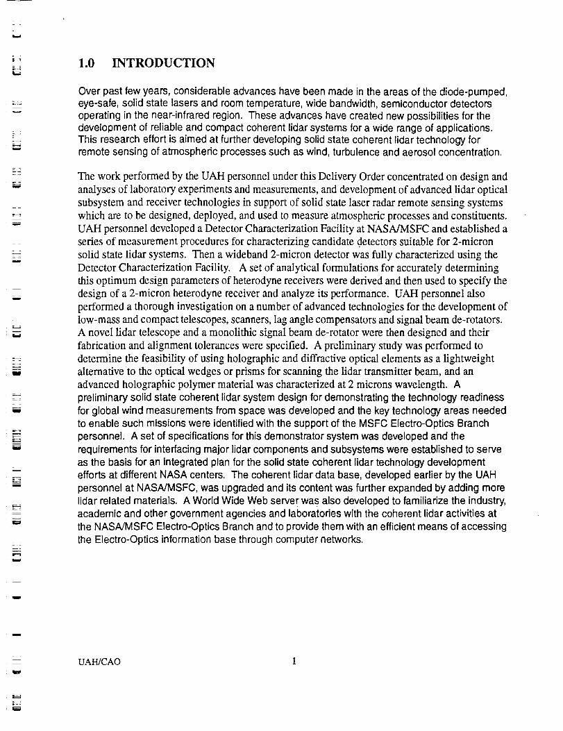
1.0 INTRODUCTION
Over past few years, considerable advances have been made in the areas of the diode-pumped,eye-safe, solid state lasers and room temperature, wide bandwidth, semiconductor detectors
operating in the near-infrared region. These advances have created new possibilities for thedevelopment of reliable and compact coherent lidar systems for a wide range of applications.This research effort is aimed at further developing solid state coherent lidar technology forremote sensing of atmospheric processes such as wind, turbulence and aerosol concentration.
The work performed by the UAH personnel under this Delivery Order concentrated on design and
analyses of laboratory experiments and measurements, and development of advanced lidar optical
subsystem and receiver technologies in support of solid state laser radar remote sensing systems
which are to be designed, deployed, and used to measure atmospheric processes and constituents.
UAH personnel developed a Detector Characterization Facility at NASA/MSFC and established a
series of measurement procedures for characterizing candidate detectors suitable for 2-micron
solid state lidar systems. Then a wideband 2-micron detector was fully characterized using the
Detector Characterization Facility. A set of analytical formulations for accurately determining
this optimum design parameters of heterodyne receivers were derived and then used to specify the
design of a 2-micron heterodyne receiver and analyze its performance. UAH personnel also
performed a thorough investigation on a number of advanced technologies for the development of
low-mass and compact telescopes, scanners, lag angle compensators and signal beam de-rotators.
A novel lidar telescope and a monolithic signal beam de-rotator were then designed and their
fabrication and alignment tolerances were specified. A preliminary study was performed to
determine the feasibility of using holographic and diffractive optical elements as a lightweight
alternative to the optical wedges or prisms for scanning the lidar transmitter beam, and an
advanced holographic polymer material was characterized at 2 microns wavelength. A
preliminary solid state coherent lidar system design for demonstrating the technology readiness
for global wind measurements from space was developed and the key technology areas needed
to enable such missions were identified with the support of the MSFC Electro-Optics Branchpersonnel. A set of specifications for this demonstrator system was developed and the
requirements for interfacing major lidar components and subsystems were established to serve
as the basis for an integrated plan for the solid state coherent lidar technology developmentefforts at different NASA centers. The coherent lidar data base, developed earlier by the UAH
personnel at NASA/MSFC, was upgraded and its content was further expanded by adding morelidar related materials. A World Wide Web server was also developed to familiarize the industry,
academic and other government agencies and laboratories with the coherent lidar activities at
the NASA/MSFC Electro-Optics Branch and to provide them with an efficient means of accessing
the Electro-Optics information base through computer networks.
w
w
W
UAH/CAO l
2.0 DETECTOR CHARACTERIZATION
2.1 INTRODUCTION
A Detector Characterization Facility (DCF), capable of measuring 2-micron detection devices and
evaluating heterodyne receivers, was developed at the Marshall Space Flight Center. The DCF is
capable of providing all the necessary detection parameters for design, development and calibra-
tion of coherent and incoherent solid state laser radar (lidar) systems. The coherent lidars in par-
ticular require an accurate knowledge of detector heterodyne quantum efficiency 13, nonlinearity
properties 4-7 and voltage-current relationship 7-9' as a function of applied optical power. At
present no detector manufacturer provides these quantities or adequately characterizes their detec-
tors for heterodyne detection operation. In addition, the detector characterization facility mea-
sures the detectors DC and AC quantum efficiencies noise equivalent power and frequency
response up to several GHz. The DCF is also capable of evaluating various heterodyne detection
schemes such as balanced detectors and fiber optic intefferometers. The design and analyses of
measurements for the DCF was performed over the previous year and a detail description of its
design and its capabilities was provided in the NASA report NASS-38609/DO777. It should also
be noted that the DCF design was further improved to allow for characterization of diffractive and
holographic optical elements and other critical optical components of coherent lidar systems.
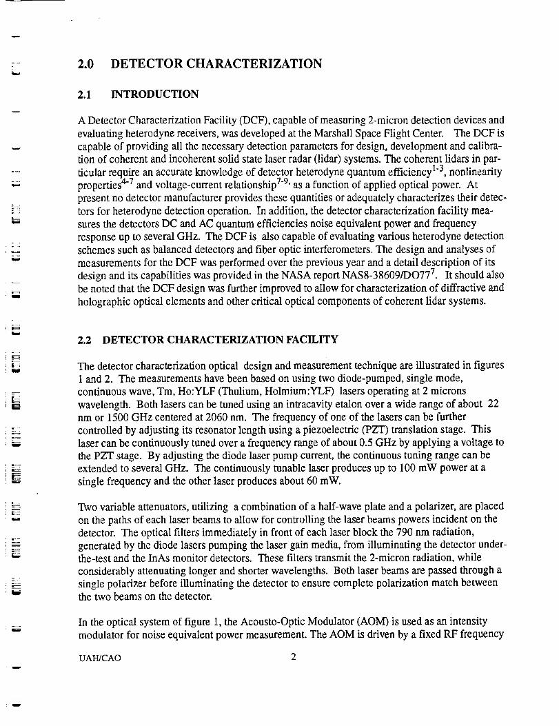
2.2 DETECTOR CHARACTERIZATION FACILITY
The detector characterization optical design and measurement technique are illustrated in figures
1 and 2. The measurements have been based on using two diode-pumped, single mode,
continuous wave, Tm, Ho:YLF (Thulium, Holmium:YLF) lasers operating at 2 microns
wavelength. Both lasers can be tuned using an intracavity etalon over a wide range of about 22
nm or 1500 GHz centered at 2060 nm. The frequency of one of the lasers can be further
controlled by adjusting its resonator length using a piezoelectric (PZT) translation stage. This
laser can be continuously tuned over a frequency range of about 0.5 GHz by applying a voltage to
the PZT stage. By adjusting the diode laser pump current, the continuous tuning range can be
extended to several GHz. The continuously tunable laser produces up to 100 mW power at a
single frequency and the other laser produces about 60 roW.
Two variable attenuators, utilizing a combination of a half-wave plate and a polarizer, are placed
on the paths of each laser beams to allow for controlling the laser beams powers incident on the
detector. The optical filters immediately in front of each laser block the 790 nm radiation,
generated by the diode lasers pumping the laser gain media, from illuminating the detector under-
the-test and the InAs monitor detectors. These filters transmit the 2-micron radiation, while
considerably attenuating longer and shorter wavelengths. Both laser beams are passed through a
single polarizer before illuminating the detector to ensure complete polarization match betweenthe two beams on the detector.
In the optical system of figure 1, the Acousto-Optic Modulator (AOM) is used as an intensity
modulator for noise equivalent power measurement. The AOM is driven by a fixed RF frequency
UAH/CAO 2
w
n
w
u
w
J
w
signal modulated by an adjustable amplitude and frequency signal. The AOM in turn modulates
the laser beam intensity eliminating the need for using a mechanical chopper which can degrade
the measurement accuracy. The chopper transmission function is highly variant depending on the
position of the beam on the chopper wheel and its rotation frequency. Therefore, using a
mechanical chopper would require frequent calibration that are tedious to perform and can affect
the measurements repeatability.
The DCF can operate in both direct and heterodyne detection modes. In heterodyne detection
mode, both lasers are used to illuminate the detector under-the-test and for the direct detection
measurements, the output of one of the lasers is blocked. For direct detection measurements, the
output of the continuously tunable laser is first measured by a precision power meter and
thereafter is monitored by an InAs detector. The InAs detector has a 200 KHz bandwidth, which is
more than sufficient for measuring any variation in the laser output power that may occur during
the measurement procedure. For these measurements, a short focal length lens (25 mm) is placed
in front of the detector being characterized. The short focal length lens will focus the beam to a
spot size considerably smaller than the detector effective area to avoid introducing any truncation
error in the measurements. The detector output is then amplified by an electronic receiver to be
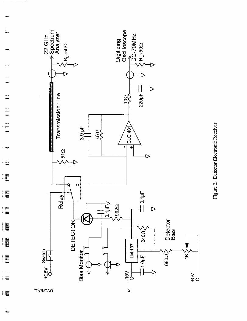
measured. The receiver also operates in two different modes, accordingly with direct and
heterodyne detection measurement modes, using a manual switch and an on-line relay (figure 2).
For the direct detection measurements, the receiver relay directs the detector signal towards an
amplifier. The amplified signal is then measured by a precision digital voltmeter. For heterodyne
detection measurements, the relay directs the signal directly through a transmission line,
terminated at both ends by 50 ohms, to a wideband (21 GHz) spectrum analyzer.
The detector frequency response and heterodyne quantum efficiency are measured in heterodyne
detection mode. For these measurements, the outputs of the lasers are focused by two long focal
length (75 cm) lenses and then combined by a beam splitter at the detector. By mixing the two
laser beams, the detector generates a current at the difference frequency between the two lasers.
By varying the frequency of the continuously tunable laser and measuring the detector signal
amplitude, the detector frequency response can be determined. The amplitude of the detector
signal at the difference frequency is directly related to the product of the DC currents due to the
individual beams and the detector's heterodyne quantum efficiency. Therefore by normalizing the
detector IF signal power by the amplitudes of the detector DC components, the detector
heterodyne quantum efficiency can be obtained as a function of signal frequency. Since the
detector frequency response is related to the bias voltage, these measurements are repeated for
different applied reverse-biased voltages.
The electronic receiver performs three functions: amplifying detector output current, interfacing
the detector and the measurement instrument, and providing bias voltage to the detector. The
operation of the receiver is shown in figure 2. The receiver uses an adjustable constant voltage
source for providing the bias voltage to the detector, a high frequency relay for directing the
detector output current, a DC-coupled transimpedance amplifier for direct detection
measurements, and a 2 ft long high frequency transmission line for carrying the IF signal to the
spectrum analyzer for heterodyne detection measurements. The transimpedance amplifier has a
moderate gain (Wout/Iin) of about 600 and a bandwidth of about 70 MHz. The amplifier is a
UAH/CAO 3
w
L_
iF1
l
ill
W
1
: r
rii
j
oo
.mI,--
o.>_ x
-%
x ¢-_,.9
o
t-O
°_(/}
0
"°°I__ t=
Direct Det. S • .- _
71o ooHet. IF S _-_ o_.__, t- _ __co< n,'__
"'- ' !___0
,4,-, I,,.,,.}
O(D__"0"
:: °,_
< _- -I_
¢
W _oz _ o.,..., .,__ _ ,.._ "_i _ •a. n_= o _ • o
UJ •o.. :_'r <_ _.__ _ _
__-o_'"'"' ____[_]--_ ..........................-_"' l.IJ W _ _ ..'_ Ii
-- _ _*
w _ Ii _ "_oo ...........................................l_ __,_w._ = iilE -_
o®
E
t-
m
_.r__l.c
i. -;......I
r_
n-iO
t_
o e_t
__.___2_oco
UAH/CAO
¢...)
©
o
0
It
UAH/CAO 5
OOtl)_
"_.__
O ,e-
>
+(
g_
0
!
u
= =
w
w
J
m
w
w
i
mw
Current Feedback (CF) operational amplifier with an input impedance of about 50 ohms. The low
input impedance ensures that virtually all the detector current will flow into the amplifier, since
the internal resistance of the InGaAs detectors are typically of the order of hundreds of kilo ohms.
The receiver uses an adjustable voltage regulator as a constant voltage source for providing bias
for the detector under-the-test. The detector bias voltage can be varied from +0.2 V to -5.0 V.
The receiver provides output ports for measuring the applied bias voltage and monitoring the
current flowing through the detector. By varying the applied bias voltage and measuring the
detector current, a family of V-I curves for different applied optical power can be obtained. These
curves along with the detector linearity and frequency response properties are necessary for
determining the detector optimum local oscillator power and bias voltage for operation in a
coherent lidar system.
As shown in figure 1, part of each laser beam is split and directed toward a fiber optic assembly
that allows the evaluation of fiber optic heterodyne receivers. The two laser beams are coupled
into two optical fibers to be mixed by a variable fiber optic coupler. The output of the coupler is
then directed through another optical fiber toward a detector. This fiber optic interferometer
assembly is capable of characterizing the optical fiber transmission properties and the coherent
mixing efficiencies of fiber optic couplers. The variable coupler used in the fiber optic
interferometer assembly will also allow the optimum mixing ratio of the signal and local oscillator
to be determined experimentally. The same setup can also be used for evaluating balanced
detectors receivers by using the second coupler output pigtail fiber to illuminate another detector
simultaneously.
Also shown in figure 1 is a combination of a beamsplitter and two mirrors that splits a portion of
the one of the lasers output and directs it towards a measurement setup for characterizing
Holographic and Diffractive Optical Elements (HOE/DOE). HOE and DOE technologies have
been studied as alternatives to optical wedge for scanning the lidar beam. The holographic and
diffractive optical elements have the potential of substantially reducing the mass of the lidar
systems and allowing for a much easier spacecraft accommodation design.
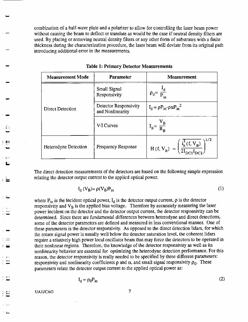
2.3 PRINCIPLES OF DETECTOR MEASUREMENTS
The DCF is capable of measuring all the necessary parameters for design, analysis and calibration
of laser radar systems. Most of the detector parameters are measured directly and the remaining
are deduced from measured quantities through simple mathematical manipulations. The primary
detector parameters that are measured are listed in table 1.
The primary parameters that are measured direct detection measurements are listed in table 1.The
detector parameters that will be measured by using a single laser beam (direct detection) are
summarized in table 1. All the direct detection measurements are performed by the continuously
tunable laser without having to readjust the mirrors or beam splitters for each measurement. It is
particularly undesirable to readjust the angular position of the beam splitters, since their
transmission to reflection ratios have a angular dependency. The variable attenuator utilizes a
UAH/CAO 6
i
m
combination of a half-wave plate and a polarizer to allow for controlling the laser beam power
without causing the beam to deflect or translate as would be the case if neutral density filters are
used. By placing or removing neutral density filters or any other form of substrates with a finite
thickness during the characterization procedure, the laser beam will deviate from its original path
introducing additional error in the measurements.
Table 1: Primary Detector Measurements
w
m
Iiw
w
w
w
w
Measurement Mode
Direct Detection
Heterodyne Detection
Parameter Measurement
Small Signal
Responsivity
Detector Responsivity
and Nonlinearity
V-I Curves
Frequency Response
I d
P0= Pin
Id = PPin-pCt.Pin 2
V B
IB- R B
H (f, VB)
"_1/2:.2
lh (f, V B )
2IDclIDc2_
The direct detection measurements of the detectors are based on the following simple expression
relating the detector output current to the applied optical power.
I d (VB)= p(VB)Pin (1)
where Pin is the incident optical power, Id is the detector output current, p is the detector
responsivity and V B is the applied bias voltage. Therefore by accurately measuring the laser
power incident on the detector and the detector output current, the detector responsivity can be
determined. Since there are fundamental differences between heterodyne and direct detections,
some of the detector parameters are defined and measured in less conventional manner. One of
these parameters is the detector responsivity. As opposed to the direct detection lidars, for which
the return signal power is usually well below the detector saturation level, the coherent lidars
require a relatively high power local oscillator beam that may force the detectors to be operated in
their nonlinear regions. Therefore, the knowledge of the detector responsivity as well as its
nonlinearity behavior are essential for optimizing the heterodyne detection performance. For this
reason, the detector responsivity is really needed to be specified by three different parameters:
responsivity and nonlinearity coefficients p and o_, and small signal responsivity P0. These
parameters relate the detector output current to the applied optical power as:
Id = P0Pin (2)
_ UAH/CAO 7
w
m
w
w
[]I
w
m
w
u
L_
I d = PPin-POCPin 2 (3)
To determine these parameters, the detector output current is measured as a function of applied
optical power. The small signal responsivity is obtained by making a least-squares fit to Eq. (1) at
low optical powers, and the responsivity and nonlinearity are determined by making a least-
squares fit to Eq. (3). The measurement of the detector responsivities and nonlinearity coefficient
are then performed at different bias voltage levels. Section 2.5 includes the results of these
measurements for a 75 microns diameter InGaAs detector.
Eq. (1) can be written as:
I d (V B) = (_V)rlDc(VB)Pin (4)
where riD C is the detector DC quantum efficiency, e is electron charge, h is Planck's constant, v is
the laser frequency. By comparing Eq. (2) and Eq. (4), the detector DC quantum efficiency can be
written as:
hvViDC (VB)= ( "_")p0 (VB) (5)
Another detector primary parameter is the detector voltage-current relationship for different
optical power levels. The V-I curves are obtained by measuring the current flowing through the
detector as a function of applied voltage across the detector for different applied optical power
levels. The V-I curves are required for specifying the detector optimum bias voltage and bias
resistor value in a heterodyne receiver, and for estimating the detector dark current noise. In
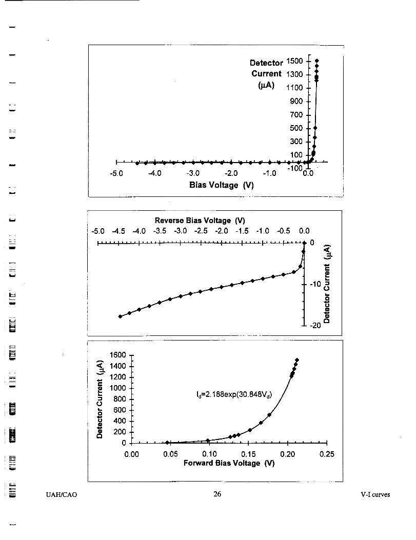
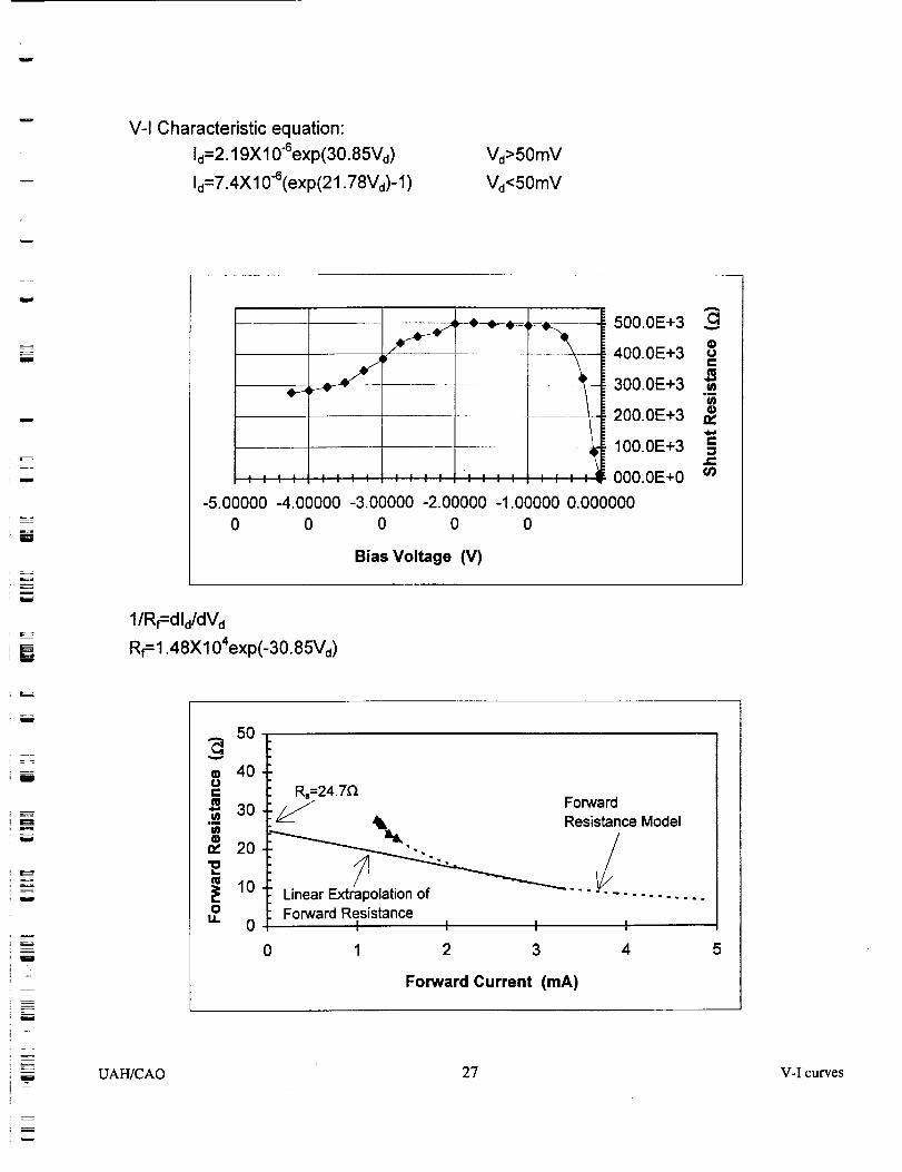
addition, the V-I curves provide the data for estimating the detector series and shunt resistances.
As discussed in section 3.1, the detector series resistance can play significant role in the
performance of wideband heterodyne receivers. The detector shunt resistance at the operating
reverse bias voltage V B is equal to
0V B
R o - OiB (6)
The shunt resistance can be simply estimated by using two sets of points on the measured V-I
curve and make a linear estimation of its slope (see section 2.5). The series resistance is
determined by first making a least-squares fit to the detector diode model using the measured data
at forward bias voltages. The detector diode model is given by:
I d = Ioe (7)
where Io is the detector saturation current and m is a empirical constant between 1 and 2. The
detector forward resistance is equal to
UAH/CAO 8
m
= :
m
w
_r_I
! i
dVd mKT-(m )VdRf- di d - ei ° e
(8)
The series resistance is estimated by evaluating Rf at relatively large forward bias currents and
then is linearly interpolated at zero bias current. On page 26, this procedure has been shown
graphically for an actual set of measured data.
The primary parameter measured in heterodyne detection mode is the detector frequency response
function. For the heterodyne detection measurements, the short focal length lens immediately in
front of the detector is removed from the optical path. First, the detector DC currents due to each
beam are measured individually. At this stage, the receiver is set to operate in the direct detection
mode, i.e., with the relay switched to the amplifier. Then, the receiver is switched to the
heterodyne detection mode and both beams are allowed to illuminate the detector. The two laser
beams are combined by a 50% beamsplitter and directed toward the detector. The detector in turn
generate a signal with a frequency equal to the frequency difference between the two beams. The
amplitude of this signal is directly related to the product of the DC currents due to the individual
beams. The detector frequency response can then be determined by measuring the heterodyne
signal power and normalizing it by the product of the DC currents due to the individual beams
while varying the frequency of the continuously tunable laser. The expression below shows the
relationship between the detector frequency response and the measured detector output currents.
/ 2 "xl/2
15 (f' vB) /H (f, VB) = _.2IDcllDc2)
(9)
The heterodyne detection measurements can be best described by the heterodyne detection
equation below that relates the detector heterodyne signal current (i n) to the laser beams powers,
P1 and P2, incident on the detector.
e) 1/2i h (f) = 2 _ rlAc (f) Fo 4ff_lP2Cos (COl - co2) t (10)
Where oh and o,x2 are the corresponding laser frequencies, _AC is the detector AC quantum
efficiency at frequency f=2n(COl-CO2), and F0 is the signal power reduction factor that accounts for
the loss of signal power due to imperfect wavefronts matching and optical misalignment. Taking
the mean-square of the heterodyne current, we obtain the heterodyne signal power.
.2 ( e "_2 2lh(f ) = 2_._-_) rlAc(f)FoPlP2 (11)
Normalizing Eq. (11) by the individual DC currents due to P1 and P2 given by Eq. (4), we canwrite
m
w
UAH/CAO 9
s
i
= =
w
w
J
w
iim._
__=
w
m
i
.2 2
t h (f) 2rlac (f)-- 2 Fo
IDCIIDc2 _DC
Rewriting the expression above as
( 2 11:2rlAC (f) = _.2IDcIlDc 2 (rlDc/Fo) )
(12)
(13)
By comparing Eq. (13) with eq. (9), the AC heterodyne quantum efficiency can be written in
terms of the detector frequency response function, as following
qAC (f) = rIDcH (f) (14)
where the signal reduction factor F0 is set equal to 1. It has been shown previously 7 that any
reduction in the heterodyne signal power due to the optical misalignment and beams wavefronts
mismatch for the measurement system of figure 1 will be negligible and F o will be essentially
unity for the DCF heterodyne detection measurements. Therefore by quantifying the detector DC
quantum efficiency as described earlier and measuring the heterodyne signal power and the direct
detection DC currents due to the individual beams, the detector frequency response and AC
quantum efficiency can be determined. The heterodyne signal power and the DC currents are
related to the receiver output voltages as:
m_.'_ You t
lh- 2 (15)gl (f)
Vout(16)
IDC- g:
where gl and g2 are the receiver gains corresponding to each channel, gl is equal to the equivalent
impedance of the transmission line terminating resistors, that is 25; and g2 is equal to the product
of the transimpedance amplifier gain and the low-pass filter transmission (see figure 2). The
values of g 1 and g2 for the receiver of figure 2 are 25 and 518, respectively.
For an ideal shot noise-limited coherent lidar, the signal to noise ratio (SNR) is equal to
2
S qAc_HPs
N - rlDchVBIF(17)
w
UAH/CAO 10
= =
where lqH is the heterodyne mixing efficiency and Ps is the return signal power.
lidar SNR is often expressed as
The coherent
w
W
S qHQErlHPs
N - hvBiF(18)
where the quantity rlHQE, referred to as the "detector heterodyne quantum efficiency", and is
equal to
2
I]AC
rlt-ieE - rlDc(19)
In Eq. (19), rlH is a system parameter that quantifies the lidar optical heterodyne efficiency while
rlHQE is a detector parameter that quantifies the efficiency of the detector in generating an ACelectrical current at the difference frequency between the local oscillator and signal beams
frequencies. Substituting Eq. (13) in Eq. (19), the detector heterodyne quantum efficiency can be
written in terms of the measured detector output currents.
i_ (f)
lqHQ E (f) - 2IDcIIDc 2 (rlDc/Fo)(20)
w
U
m
--,=
w
The heterodyne quantum efficiency may also be written in terms of the detector frequency
response, specifies as a primary measured parameter.
_HQE (f) = rlDC H2 (f) (21)
It should be noted that in Eqs. (10)-(21), the detector frequency response function H, AC quantum
efficiency rlAC and heterodyne quantum efficiency riHQE are functions of applied bias voltage
VB. However for clarity reason, the bias voltage dependance has not been shown.
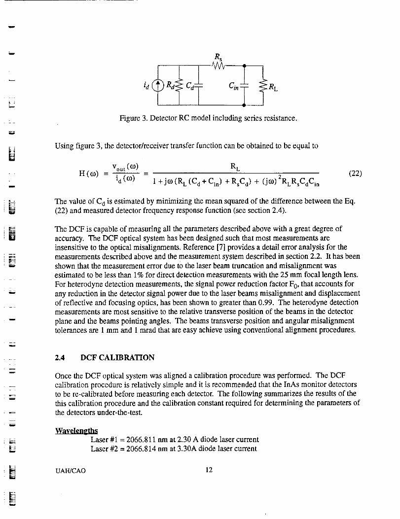
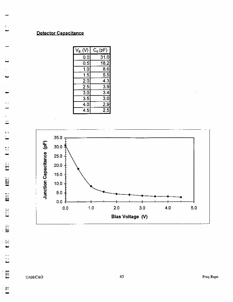
Another detector parameter that can be extracted from the frequency response function is the
detector junction capacitance. As explained in next chapter, the detector junction capacitance is
one of the critical parameters for optimizing the heterodyne receiver performance and is usually
the limiting factor for the receiver bandwidth. For determining the detector junction capacitance,
the detector RC model is used without ignoring the detector series resistance (see section 3.1).
Using the detector model, the detector/receiver transfer function is obtained and least-squared
fitted to the measured frequency response function to determine the detector junction capacitance.
The detector RC model is shown in figure 3, where R L and Cin are the input resistance and
capacitance of the DCF receiver, respectively.
UAH/CAO 11
w
i
w
L :
F ::
U
u
H
w
w
m_
i
=
R S
Figure 3. Detector RC model including series resistance.
Using figure 3, the detector/receiver transfer function can be obtained to be equal to
You t (_) R E
H(t.O) - id(_ ) -- 1 +jc0(RL(Cd+Cin) +RsCd) + (Jr'°) 2RLRsCdCin (22)
The value of C a is estimated by minimizing the mean squared of the difference between the Eq.
(22) and measured detector frequency response function (see section 2.4).
The DCF is capable of measuring all the parameters described above with a great degree of
accuracy. The DCF optical system has been designed such that most measurements are
insensitive to the optical misalignments. Reference [7] provides a detail error analysis for the
measurements described above and the measurement system described in section 2.2. It has been
shown that the measurement error due to the laser beam truncation and misalignment was
estimated to be less than 1% for direct detection measurements with the 25 mm focal length lens.
For heterodyne detection measurements, the signal power reduction factor F o, that accounts for
any reduction in the detector signal power due to the laser beams misalignment and displacement
of reflective and focusing optics, has been shown to greater than 0.99. The heterodyne detection
measurements are most sensitive to the relative transverse position of the beams in the detector
plane and the beams pointing angles. The beams transverse position and angular misalignment
tolerances are 1 mm and 1 mrad that are easy achieve using conventional alignment procedures.
2.4 DCF CALIBRATION
Once the DCF optical system was aligned a calibration procedure was performed. The DCF
calibration procedure is relatively simple and it is recommended that the InAs monitor detectors
to be re-calibrated before measuring each detector. The following summarizes the results of the
this calibration procedure and the calibration constant required for determining the parameters ofthe detectors under-the-test.
Laser #1 = 2066.811 nm at 2.30 A diode laser current
Laser #2 = 2066.814 nm at 3.30A diode laser current
UAH/CAO 12
Transmission Line
R L = 25.35 f2
Cin = 0.4 pF
Amplifier
VB=0
m
u
No Optical Beam #1 Beam #2Power
Transmission Line 0 8.04 1.04
Amplifier -2 180.6 21.6
Ratio (Amp/Trans. Line) 22.71 22.79
Fmw
Conversion factor (Amplifier to Transmission Line) = 1/22.75
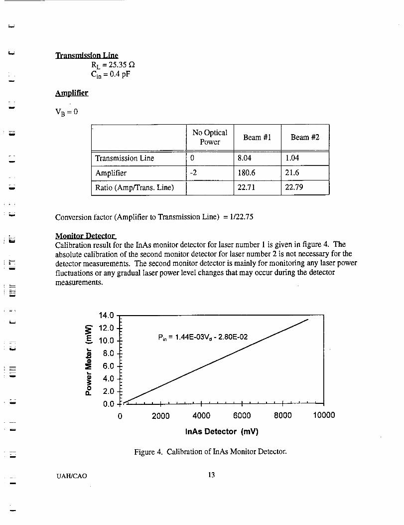
Monitor Detector
Calibration result for the InAs monitor detector for laser number 1 is given in figure 4. The
absolute calibration of the second monitor detector for laser number 2 is not necessary for the
detector measurements. The second monitor detector is mainly for monitoring any laser power
fluctuations or any gradual laser power level changes that may occur during the detector
measurements.
w
u
w
i i
14.0
i 12.0
10.0
8.0
6.0
_o 4.02.0
O.O-.F- ' ' , ' I .... ,' .... ' ....
0 2000 4000 6000 8000 10000
InAs Detector (mY)
Figure 4. Calibration of InAs Monitor Detector.
UAH/CAO 13
!
w
2.5 CHARACTERIZATION OF A 2-MICRON InGaAs DETECTOR
A 75 microns diameter InGaAs detector with a cutoff wavelength of 2.5 microns, acquired from
Sensors Unlimited, Inc., was fully characterized in the NASA/MSFC Detector Characterization
Facility. The results of the measurements are provided in this section. These results were then
used to determine the optimum design parameters of a heterodyne receiver as a function of
operating bandwidth. The heterodyne design analysis and the receiver design are described in the
next chapter.
The following data are the results of the detector measurements performed in the DCE The
detector model number is SU75-2.5-TO and its serial number is 8364-PIN.
w
m
E-
w
u
w
m
E
J
mm
w
UAIMCAO 14
m
mw
w RESPONSIVITY AND LINEARITY MEASUREMENTS
w
W
W
_N
w
--=w
L
i
VB=0.00V
Notes: Detector anode terminated by 50 ohms
With laser beam blocked, InAs laser power monitor detector reads 19.2 mV and
detector direct output is 0.0 mV.
InAs Power
Monitor (mV)
Detector
Output (mV)
203306
Incident Power
Pin (mVV)
Detector current
ld (mA)154 11.1 0.194 0.2160
15.023.0
30.436.4
410
0.2640.4:13
0.562
0.704508;609_
0.29180.44750.59140.70820.807441.5 0.849
750 47.0 1.052 0.9144902 52.4 1.271 1.0195
1108 58.2 1,568 1.1323
1300 62.3 1.844 1.21211504 66.1 2.138 1.28601756 70.1 2.501 1.36382025 73.6 2.888 1.43192260 76.2 3.226 1.48252512 78.7 3.589 1.53112745 80.7 3.925 1.5700
3003 82.6 4.296 1.60703258 84.2 4.664 1.6381
1.66933520 85.8 5.041
3.0A
L
1.o
0.0
0.000
u
.B
Id 1 04P i "
,, ,,'"" = . . 1-0.21Pin )
.... I .... : .... I .... _ .... I ' ' " '
0. 500 1.000 1. 500 2. 000 2. 500 3. 000
Power (mW)
UAH/CAO 15 Responsivity
=
=
w
W
_2
Vs=l.000 V
VBi=1.008 V
Notes:
With laser beam blocked, InAs laser power monitor detector reads 19.7 mV and
detector direct output is 0.4 mV.
InAs Power
Monitor (m_
Detector
Output (m_
Incident Power
Pin (mV_
143 10.2 0.178
204 14.8 0.266
302 22.2 0.407
407 30.2 0.558
507 37.7 0.702
41.6
50.6
603 0.840
1.05275O
910 53.7 1.282
1120 55.1 1.585
1316 55.9 1.867
1504 56.4 2.138
57.01753
2012 57.4
2.496
2.869
2250 57.6 3.212
2530 57.9 3.615
2760 58.1 3.946
3000 58.2 4.292
Detector current
I_ (mA)
0.1907
0.2802
0.4241
0.5798
0.7257
0.8016
0.9767
1.0370
1.0642
1.0798
1.0895
1.1012
1.1089
1.1128
1.1187
1.1226
1.1245
3290 58.4 4.710 1.1284
3505 58.5 5.019 1.1304
i
--4r_
JBd_J
w
3.0
_ 2.5 .,, .,.o.,.'''"'""
_. 2.0 B_ BB
"_ 1.5 Id=l.04Pi.,,,,-'"" "Id=l.14Pi.(1-0.24Pi.)?1.0 ,_ x 'x -x------..._x
,,,o.5
0.0 ' ' I ' ' ' ' I ....i
0.000 0.500 1.000 1.500 2.000 2.500 3.000
Power (mW)
wUAFUCAO 16 Responsivity
w
i
w
w
U
J
w
VB=1.505 V
VBi=1.514 V
Notes:
With laser beam blocked, lnAs laser power monitor detector reads 19.4 mV and
detector direct output is 0.4 mV.
InAs Power
Monitor (mV)
150
2O5302
Detector
Output (mV)
11.7
16.223.7
Incident Power
Pin (mW)
0.188'0.267
0.407404 31.1 0.554
508 38.4 0.704
600 45.0 0.836768 57.6 1.078922 69.1 1,300
1114 74.2 1,5761350 77.3
78.279.180.0
1513
81.8
1740i2067
1.9162.1512.4782.948
2247 80.3 3.2082490 80.7 3.5582792 81.1 3.9923020 81.3 4.3213280 81.6 4,6953554 5.090
Detector current
Id (mA)
0.21980.3074
0.45330.5973
0.7393
0.86771.11281.33661.43581.4961
1.51361.53111.54861.55451.56231.57001.57391.57981.5837
w
m
w
W
m
3.0
'_ 2.0
(_ 1.5t_
1.0u
a0.5
0.0
0.000
,w
Id=1 "05Pin , ,- x_,_,w.. _ _' x" _ ""-'-w--,......,.,_
i i ! • I! ! | ! I !1 I ! I I ,l t • | !
1.000 2.000 3.000
Power (mW)
4.000
E
mUAH/CAO 17 Responsivity
L
i
w
w
w
w
w
---=
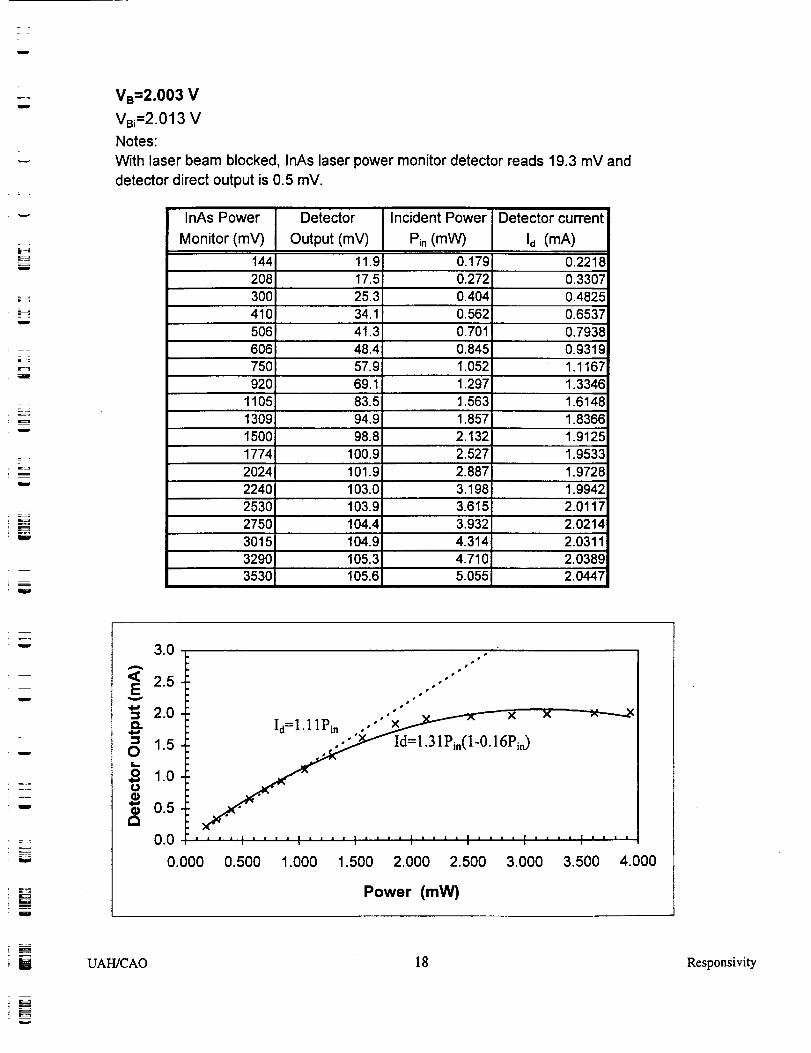
VB=2.003 V
VBi=2.013 V
Notes:
With laser beam blocked, InAs laser power monitor detector reads 19.3 mV and
detector direct output is 0.5 mV.
InAs Power
Monitor (mV)
Detector
Output (mV)
Incident Power
Pin (mW)
144 11.9 0.179208 17.5 0.272300 25.3 0.404
410 34.1 0.562506 41.3 0.701606 48.4 0.845
57.975O 1.052920 69.1 1.297
1105 83.5 1.5631309 94.9 1.8571500 98.8 2.132
100.9101.9
17742024
2.5272.887
2240 103.0 3.198
2530 103.9 3.6152750 104.4 3.932
104.9105.3
301532903530 105.6
4.3144.7105.055
Detector current
Id (mA)
0.2218
0.3307_0.48250.65370.79380.93191.11671.3346
1.61481.83661.91251.95331.97281.9942
2.01172.02142.03112.03892.0447
w
w
w
Mw
.9o 1.oU
"$ 0.5
0.0
0.000
",_x xId= 1. 11
P_.._'_'-" Id= 1.31 Pin(1-0.16P_,,)
, , , _ _ i i i i _ L , , , tl . . . , i, . , _ _ nl ' ' ' ' l, _ , , . ,i , • •
0.500 1.000 1.500 2.000 2.500 3.000 3.500 4.000
Power (mW)
B UAH/CAO 18 Responsivity
w
E
=w
m
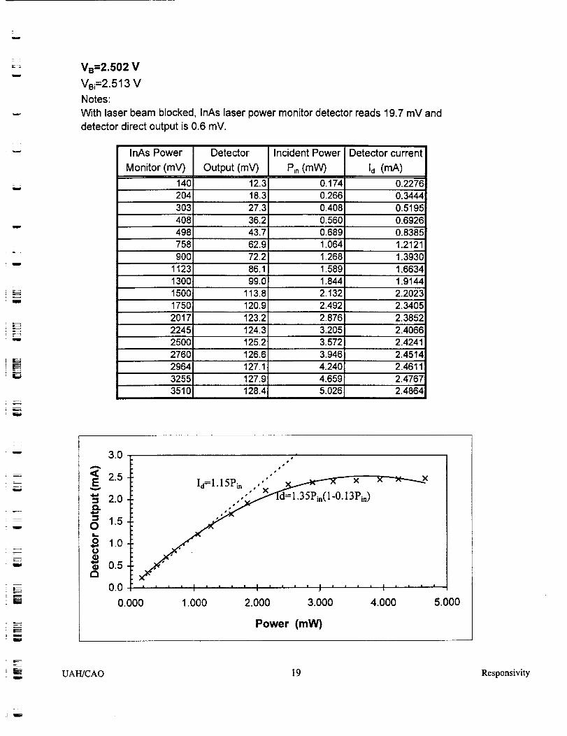
VB=2.502 V
VBi=2.513 V
Notes:
With laser beam blocked, InAs laser power monitor detector reads 19.7 mV anddetector direct output is 0.6 mV.
InAs Power
Monitor (mV)
140204
Detector
Output (mV)
12.318.3
Incident Power
Pin (mVV)
0.1740.266
Detector current
Id (mA)
0.22760.3444
303 27.3 0.408 0.5195
408 36.2 0.560 0.6926498 43.7 0.689 0.8385758 62.9 1.064 1.2121900 72.2 1.268 1.3930
1123 86.1 1.589 1.66341300! 99.0 1.844 1.91441500 113.8 2.132 2.20231750 120.9 2.492 2.3405
2017 123.2 2.876 2.38522245 124.3 3.205 2.40662500 125.2
126.63.572 2.4241
2760 3.946 2.45142964 127.1 4.240 2.46113255 4.6593510 5.026
127.91128.4
2.47672.4'864
u
w
w
w
i
L
1.o(.1
a
0.0
0.000
_'° j'''
e" X
Id=l.15Pin .,' x
=1.35Pi.(l-0. l3Pin)"" x
.... I .... I ' , , , I ........• |
1.000 2.000 3.000 4.000
Power (mW)
|
5.000
wUAH/CAO 19 Responsivity
=
w
w
w
W
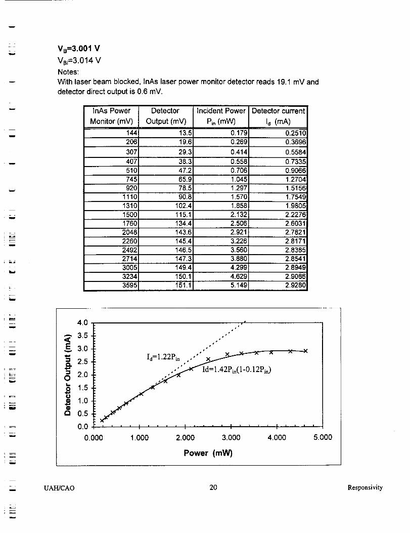
Vs=3.001 V
VBi=3.014 V
Notes:
With laser beam blocked, InAs laser power monitor detector reads 19.1 mV and
detector direct output is 0.6 mV.
InAs Power Detector
Monitor (mV) Output (mV)
144 13.5206 19.6
307 29.3
407 38.3
51074592O
111o1310150o1760
2048
47.265.978.590.8
102.4115.1134.4
143.62260 145.42492 146.52714 147.3
Incident Power
Pi. (mW)
0.1790.269
0.414
0.5580.7061.0451.2971.5701.8582.1322.5062.9213.226
Detector cu_ent
Id (mA)
0.25100.3696
0.5584
0.73350.90661.27041.51561.75491.98052.2276
2.60312.78212.8171
3.560 2.83853.880 2.8541
3005 149.4 4.299
3234 150.1 4.629
3595 151.1 5.149
2.89492.90862.9280
m
m
w
u
rmw
4.0
"_ 2.5
2.0
1.5
_ 1.0
0.0
0.000
#
#
Id=l.22Pi..,,'"
Id=1.42Pin(1-O. 12Pi.)
.... I .... 1 ........, ' t _111 I I I
1. 000 2.000 3.000 4.000 5. 000
Power (mW)
mUAH/CAO 20 Responsivity
w
;w
w
L_
g
w
lil
W
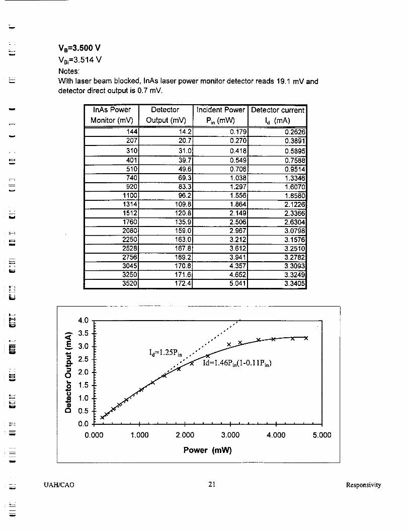
Ve=3.500 V
VBi=3.514 V
Notes:
With laser beam blocked, InAs laser power monitor detector reads 19.1 mV and
detector direct output is 0.7 mV.
InAs Power
Monitor (mV)
144207
310
Detector
Output (m_
14.2
20.7
31.0!
401 39.7510 49.6740 69.3
920 83.31100 96.2
1314 109.81512 120.81760 135.92080 159.02250 163.0
2528 167.82756 169.23045 170.83250 171.63520 172.4
Incident Power
Pin (mW)
0.179
0.270
0.418
0.5490.706
1.0381.2971.5561.8642.1492.5062.967
...... 3.212
3.6123.9414.3574.6525.041
Detector current
Id (mA)
0.26260.3891
0.5895
0.7588
0.95141.33461.60701.85802.12262.3366
2.63043.07983.15763.25103.27823.30933.32493.3405
W
-c
r__i
=m
z
4.0
_- 3.5
3.0
2.5
2.0
'- 1.5
1.o
0.0
0.000
Id=1.25Pin,,," "_
Id=1.46Pi.(1-0.1 lPi.)
| | I i iI . i • • iI I I • . iI . • • • _ ' • • l
1.000 2.000 3.000 4.000 5.000
Power (mW)
UAH/CAO 21 Responsivity
w
w
r_
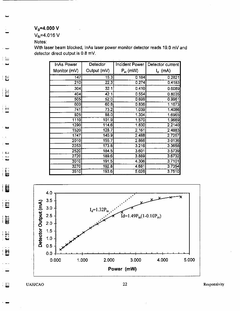
VB=4.000 V
VBi=4.016 V
Notes:
With laser beam blocked, InAs laser power monitor detector reads 19.0 mV and
detector direct output is 0.8 mV.
InAs Power
Monitor (mV)
147:
210
304
404505600
Detector
Output (mV)
15.322.3
32.1
42.152.060.8
741 73.2925 88.O
1110 101.91290 114.61520 128.71747 140.92010 155.72253 173.8
252027203010
184.5
3510
189.6191.5
3270 192.8193.6
Incident Power
Pin (mW)
0.184
0.274
0.410
0.5540.6990.836
1.0391.304
1.5701.8302.1612.4882.8663.216
3.6013.8894.3064.6815.026
Detector current
Id (mA)
0.28210.4183
0.6089
0.80350.99611.1673
1.40861.69651.96692.21402.48832.72573.01363.3658
3.57393.67323.7101:3.73543.7510
[]
m
4.0
_" 3.5
3.0
'_ 2.5
(_ 2.0
'- 1.5
1.o0.5
0.0
0.000
w'"
s"
Id=1.32Pi.,,, "_
.'jZ Id=l AgP'"(I'O'IOPin)
' ' ' ' I .... ', .... _ .... _ ' ' '
1.000 2.000 3.000 4.000
Power (mW)
uUAH/CAO 22 Responsivity
= =
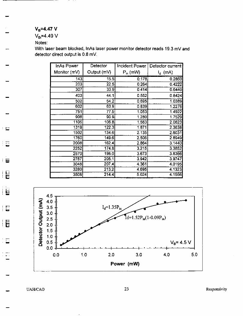
VB=4.47 V
VBi=4.49 V
Notes:
With laser beam blocked, InAs laser power monitor detector reads 19.3 mV and
detector direct output is 0.8 mV.
InAs Power
Monitor (mV)
Detector
Output (mV)
Incident Power
Pi. (mW)
Detector current
Id (mA)
0.414
143 15.5 0.178 0.2860203 22.5 0.264 0.4222307 33.9 0.6440
403 44.1 0.552
502 54.2 0.695602 63.9 0.839751 77.5 1.053908 90.9 1.280
1105 106.8
1319 122.3i134.6149.6162.4174.8
15021760200822522570
2757304832803508
198.0
1.5631.8712.1352.5062.8643.2153.673
3.9424.3614.6955.024
205.1207.4213.2214.4
0.8424
1.0389
1.22761.49221.75292.06232.36382.60312:8949
3.14403.38523.83663.9747
4.01954.1'323
4.1556
u
H
.===.= ,
I
Ew
4.5A
4.0E 3.5
O 2.0
o 1.51.0
0.50.0
Id=|.35_
¢f Id= 1.52P_n(1-0.09Pin)
VB" 4.5 VI I | I ] • | • ' Ia i • . | tI | • • | II
0.0 1.0 2.0 3.0 4.0 5.0
Power (mW)
UAH/CAO 23 Responsivity
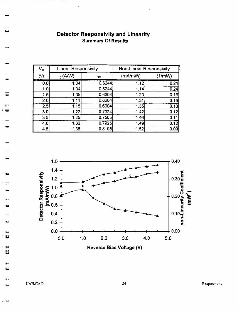
Detector Responsivity and LinearitySummary Of Results
zw
VB
0.0
1.0
1.5
2.0
2.5
3.0
3.5
4.0
4.5
Linear Responsivity
0(A/W)
Non-Linear Responsivity
(mA/mW) (l/mW)DC
1.04 0.6244 1.12 0.21
1.04 0.6244 1.14 0.24
0.6304 1.231.05 0.19
1.11 0.6664 1.31 0.16
1.15 0.6904 1.35 0.13
1.22 0.7324 1.42 0..121.25 0.7505 1146 0.11
1.32 0.7925 1.4911.520.81051.35
................... 0.100.09
_m
mE
1.6
1.4
._ 1.2
o.8go.6
0.4OGI
0.2
0.0
0.0
-.._-........._
' I i I i I ' I '
1.0 2.0 3.0 4.0
Reverse Bias Voltage (V)
0.40
0.30_
°g0.20,,_
=_0.10"'i
!
¢,-Oe-
0.00
5.0
nUAH/CAO 24 Responsivity
w
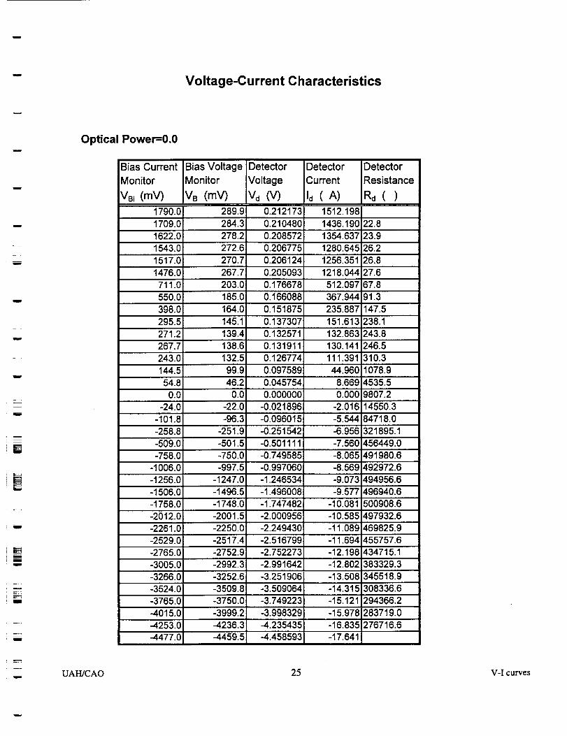
Voltage-Current Characteristics
w
m
mm
u
m
J
li
=
m
i
Optical Power=O.O
)Bias Current Bias Voltage Detector
Monitor Monitor Voltage
VBi (mV) VB (mV) (V)1790.0 289.91709.0 284.3
1622.0 278.21543.0 272.61517.0 270.7
1476.0 267.7711.0 203.0550.0 185.0
398.0 164.0295.5 145.1271.2 139.4267.7 138.6243.0 132.5144.5 99.954.8 46.20.0 0.0
-24.0 -22.0-101.8 -96.3
-258.8 -251.9-509.0 -501.5-758.0 -750.0
-1006.0 -997.5-1256.0 -1247.0-1506.0 -1496.5-1758.0 -1748.0-2012.0 -2001.5-2261.0 -2250.0-2529.0 -2517.4-2765.0 -2752.9-3005.0-3266.0
-2992.3-3252.6
-3524.0 -3509.8-3765.0 -3750.0-4015.0 -3999.2-4253.0 -4236.3-4477.0 -4459.5
Detector
Current
Id (A)
Detector
Resistance
)0.212173 1512.19801'210480 1436.190 22.8
0.208572 1354.637 23.90.206775 1280.645
1256.3510.20612426.226.8
0.205093 1218.044 27.60.176678 512.097 67.80.166088 367.944 91.30.151875 235.887 147.50.137307 151.613 238.10.132571 132.863 243.8
0.131911i 130.141 246.51tl.39144.960
0.1267740.097589
0.000000-0.021896=-0.096015
310.31078.9
0.045754 8.669 4535.50.000 9807.2
-2.016 14550.3-5.54484718.0
-0.251542 -6.956 321895.1
-0.501111i -7.560 456449.0-0.749585 -8.065 491980.6-0.997060 -8.569 492972.6-1.246534 -9.073 494956.6
-1.4960081 -9.577 496940.6-1.747482 -10.081 500908.6-2.000956! -10.585 497932.6
-11.089-11.694-12.198-12.802
-2.249430!-2.516799-2.752273-2.991642-3.251906 -13.508
469825.9
455757.6434715.1383329.3
345518.9-3.509064 -14.315 308336.6-3.749223 -15.121 294366.2-3.998329 -15.978 283719.0
-16.835-4.235435-4.458593 -17.641
276716.6
wUAH/CAO 25 V-I curves
w
Detector 1500 Ii
Current 1300 L i
(gJ_) 1100 "
900 "
7oo "]50o il
300 "t
.................................. !°.°. _'..-5.0 -4.0 "-_0"" "-2.0" "-_0" :l°'°o.b
Bias Voltage (V)
Reverse Bias Voltage (V)
-5.0 -4.5 -4.0 -3.5 -3.0 -2.5 -2.0 -1.5 -1.0 -0.5 0.0
-10 _
_'_'_ - t .20 __
_ .-. 1600"1-_" 1200+ f= lOOO
,_,.,,-,t ld=2.188exp(30.848V,_) /
. _ 6ooJ_ ./4ooF .,,"-
_i _ _OOof,,,.;:.... _...: .... 'o.oo o.o_ o.,o o.,_ o.;o o.;_Forward Bias Voltage (V)
UAH/CAO 26 V-I curves
V-I Characteristic equation:
Id=2.19Xl 06exp(30.85Vd)
Id=7.4X 10"6(exp (21.78Vd)- 1)
Vd>50mV
V_<50mV
w
i
--=w
_=
w= i = i i | |
500.0E+3 ,_
8400.0E+3
300.0E+3 ._
200.0E+3
100o0E+3 ==
000.0E+0 u_
-5.00000 -4.00000 -3.00000 -2.00000 -1.00000 0.000000
0 0 0 0 0
l/Rr=dld/dVd
Rr =1.48X 10⁴exp(-30.85Vd)
Bias Voltage (V)
imm
W
= _._
mi
m_Iii
-?UAH/CAO
5O
40
30
2O
0
Rs=24.7_
,/_ Forward• -- • Resistance Model
• " "'" "_°°'°'°-.m.
I I I I
0 1 2 3 4 5
Forward Current (mA)
27 V-I curves
w
i
w
w
= =
w
w
z
w
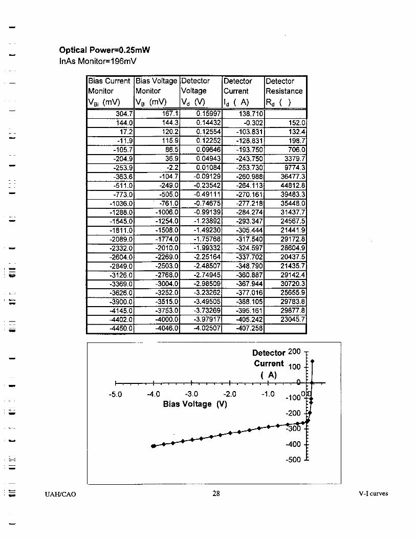
Optical Power=0.25mW
lnAs Monitor=196mV
Bias Current Bias Voltage Detector
Monitor Monitor Voltage
VBi (mY) VB (mV) Vd (V)
Detector
Current
Id (A)
Detector ....
Resistance
Rd( )
-2332.0
304.7 167.1 0.15997 138.710144.0 144.3 0.14432 -0.302 152.017.2 120.2 0.12554 -103.831 132.4
-11.9 115.9 0.12252 -128.831 198.7
-105.7 86.5 0.09646 -193.750 706.0-204.9 36.9 0.04943 -243.750 3379.7-253.9 -2.2 0.01084 -253.730 9774.3-363.6 -104.7 -0.09129 -260.988 36477.3-511.0 -249.0 -0.23542 -264.113 44812.8-773.0 -505.0 '_0.49111 -270.161 39483.3
-1036.0 -761.0 -0.74675 -277.218 35448.0-1288.0 -1006.0 -0.99139 -284.274 31437.7
-1545.0 -1254.0 -1.23892 -293.347 24567.5-1811.0 -1508.0 -1.49230 "_'305.444 21441.9
-2089.0 -1774.0 -1.75768 -317.540 29172.8-2010.0 -1.99332 28604.9
-2269.0 -2.25164-324.597-337.702i-2604.0 20437.5
-2849.0 -2503.0 -2.48507 -348.790i 21435.7
-3126.0 -2768.0 -2.74945 -360.8871 29142.4-3369.0 -3004.0 -2.98509 30720.3
-3252.0
-3515.0
-3.23262-3626.0-3.49505
-3.73269
-367.944_-377.016
-3900.0 -388.1051-395.161-3753.0
-4450.0
25655.929783.8
29877.8-4145.0-4402.0 -4000.0 -3.97917 -405.242! 23045.7
-4046.0 -4.02507 -407.258
UAH/CAO
I .... I .... I ,I
-5.0 4.0 -3.0 -2.0
BiasVol_ge(V)
Detector 200
Current 100
(A)! • , , 0
-1.0 _100 O.
28 V-I curves
=
Optical Power=O.5mW
InAs Monitor=387mV
w
w
w
F_
N
U
HU
U
Bias Current Bias Voltage Detector
Monitor Monitor Voltage
VBi (mV) VB (mV) Vd (V)
Detector Detector
Current Resistance
Id (A) Rd ( )
313.2 177.0 0.169943 137.298
161.7 160.3 0.160227 1.411 82.60.0 139.6 0.146833 -140.726 114.9
-94.6 0.136589 -221.573 144.8
-238.6 0.116282 -340.121 316.5-506.0 0.5 0.026744 -510.585 6433.0-678.0 -150.7 -0.123378 -531.552 141808.0-782.0 -254.0 -0.226642 -532.258 140405.8
-1033.0 -503.0 -0.475538 -534.274 110264.3-1301.0 -757.0 -0.728813 -548.387 14985.6-1577.0 -1007.0 -0.977466 -574.597 10399.0
-1861.0 -1268.0 -1.237274 -597.782 11568.5-2135.0 -1521.0 -1.489186 -618.952 12319.5-2384.0 -1752.0-2661.0 -2008.0-2931.0 -2261.0
-3204.0 -2516.0-3468.0 -2744.0-3756.0-4037.0-4299.0-4498.0
-3010.0
-3269.0-3509.0-3694.0
-1.719253-1.974165-2.2262841-2.480352i-2.706486-2.971346-3.229206
-3.468067-3.652341
-637.097 12384.9-658.266 13517.3-675.403 14367.1-693.548 11411.7-729.839-752.016
-774.194-796.371-810.484
9776.311785.0
11198.812167.9
I . D • • I
-4.0 -3.0 -2.0
Bias Voltage (V)
200
I .... I . . . 0
-1.0 0-200
-40O
-1000
Detector
Current
(A)
m UAH]CAO 29 V-I curves
!
1
r
um_
!
=
m
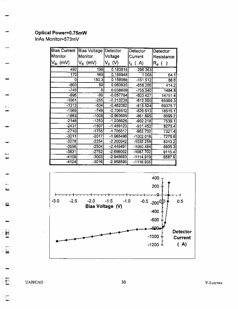
Optical Power=0.75mW
InAs Monitor=573mV
Bias Current
Monitor
VBi (mV)
Bias Voltage Detector Detector
Monitor Voltage Current
VB (mV) Vd (V) Id (A)
Detector
Resistance
Rd( )
492 199 0.183818 295.363170 169 0.168948 1.008 64.1
0 150.3 0.158088 -151.512 88.6-603 50 0.083835 -658.266 414.2-749 0 0.038809 -755.040 1484.8-896 -99 -0.057704 -803.427 14751.4
-1061-1313
-1569-1863-2148-2431
-255
-504-749
-1008-1253-1507-1755
-2017
-0.213238":0.462082
-0.706512-0.963699-1.206626-1.459123-1.705517
-1.965496
-812.500
-2.958590 i
-815.524
-626.613-861.895-902.218-931.452-962.702
-1002.016
65999.3
-1116.935
-2710-3011
-3278-3556-3831-4109-4124
69375.718515.16699.27539.18273.47321.4
7275.6-2254 -2.200942 -1032.258 8313.2-2504 -2.449491 -1060.484 8935.3
-2752 -2.696092 -1087.702 9115.4-3003 -2.945693 -1114.919 6587.9-3016
400 T
-3.0 -2.s o.s
:;;f/_ _ i'_'e'_'4'_" -..,i., _ Detector
_- ii_)_ t C_rr/_nt
mUAH/CAO 30 V-I curves
w
= =W
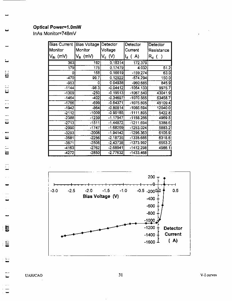
Optical Power=l.0mW
InAs Monitor=748mV
!
p-
w
r--
i
I
W
Bias Current
Monitor
VBi (mV)
Bias Voltage Detector Detector Detector
Monitor Voltage Current Resistance
VB (mV) Vd (V) Id (A) Rd ( )
363179
0-470
-953-1144-1309-1464-1766-1942
-2112-2388
-2713-2990-3293-3581..........-3871-4163-4272
192 0.18314 172.379175 0.17479 51.2158
99.7
-98.3-25O-402
0.166190.129220,04938
-0.04412-0.19513
-0.34697
4.032-159.274-574.2§4
-960.685-1054.133-1067.540i-1070.565-1075.665
63.0
-1433.468
150.0845.9
9975.743041.953458.7
-699 -0.64371 45109.4-864 -0.80814 -1086.694 12040.0
-1009 -0.95185 -1111.895 5422.8-1239 -1.17947 -1158.266 4969.5
-1511 -1.44872 -1211.694 5388.6-1747 -1.68259 -1253.024 5883.2-2008 -1.94142 -1295.363 6105.9-2256 -2.18735 -1335.685 6318.6-2508 -2.43738 -1'373.992 6553.2-2762 -2.68941 -1412.298 4986.1-2850 -2.77632
w
i
w
i
2O0
-3_ -1.5 4o o-.s-2ooopt 0.2BiasVol_ge _) 400_ /
-,oot T- ootJ
. _ -IZUU _ Detector
-1400 _ Current
-1600 (A)
UAH/CAO 31 V-I curves
w
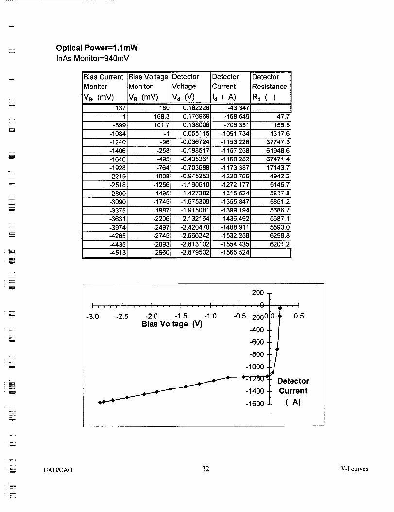
Optical Power=l .lmW
InAs Monitor=940mV
=
w
= =
i
w
w
m
Bias Current
Monitor
VBi (mV)
Bias Voltage Detector Detector
Monitor Voltage Current
VB (mY) V_ (V) I_ (A)
137
-599
-1084-1240
-1406-1646-1928
-2219-2518
-2800-3090-3375-3631-3974
180
-4513
168.3101.7
-1-96
-258
-495-764
-1008-1256-1495
-1745-1987-2206-2497
0.182228
0.1769690.1380060.055115
-0.036724-0.198517-0.435361
-0.703688-0.945253-1.190610-1.427382-1.675309-1.915081
-2.132164-2.420470
-43.347-168.649!
-706.351-1091.734-1153.226-1157.258
-1160.282-1173.387-1220.766-1272.177-1315.524-1355.847:1'399.194
-1436.492-1488.911
-4265 -2745 -2.666242 -1532.258-4435 -2893 -2.813102 -1554.435
-2960 -2.879532 -1565.524
Detector
Resistance
Rd( )
47.7155.5
1317.637747.361948.6
67471.417143.74942.25146.75817.85851.2
5686.75687.15593.06299.86201.2
w
i
D
w
w
200
-3_5
Bias Voltage (V) _400 ._ I
-ooot- oo/
_ _ --ILuu -_ Detector
_ _ " -1400 t Current(A)
..==
UAH/CAO 32 V-I curves
w
-=w
I
E
W
w
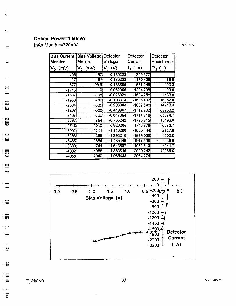
Optical Power=l.50mW
InAs Monitor=720mV
Bias Current Bias Voltage Detector Detector Detector
Monitor Monitor Voltage Current Resistance
Vei (mY) VB (mV) Vd (V) Id (A) Rd ( )
405 197 0.186223 209.677
-17 161 0.170223 -179.435 55.0-577 98.6 0.133606 -681.048 100.3
-1215 0 0.062955 -1224.798 190.9
-1687 -105 -0.023029 -1594.758 1533.6-1953 -280 -0.193314 -1686.492 16352.8-2064 -385 -0.298003 -'1692.540 14710.3
-2207 -508 -0.419967 -1712.702 89783.2-2407 -706 -0.617864 -1714.718 85874.7-2567 -854 -0.765242 -1726.815 10496.9-2743 -1010 -0.920205 -1746.976 6583.7
-3002! -1211 -1.118200 -1805.444 2927.8-3263i -1395 -1.298210 -1883.065 4500.0
-34861 -1584 -1.485449 -1917.339 5039.9-3680 -1744 -1.643687 -1951.613 4141.7
-1988 -1.883646 -2030.242 12366.9-4002-4058 -2040 -1.935438 -2034.274
2/20196
200
-3.0 0.5
:oOo11-8oo± /
-lOOO±/-1200 -_-1400
DetectorCurrent
-2200 .L (A)
UAH/CAO 33 V-I curves
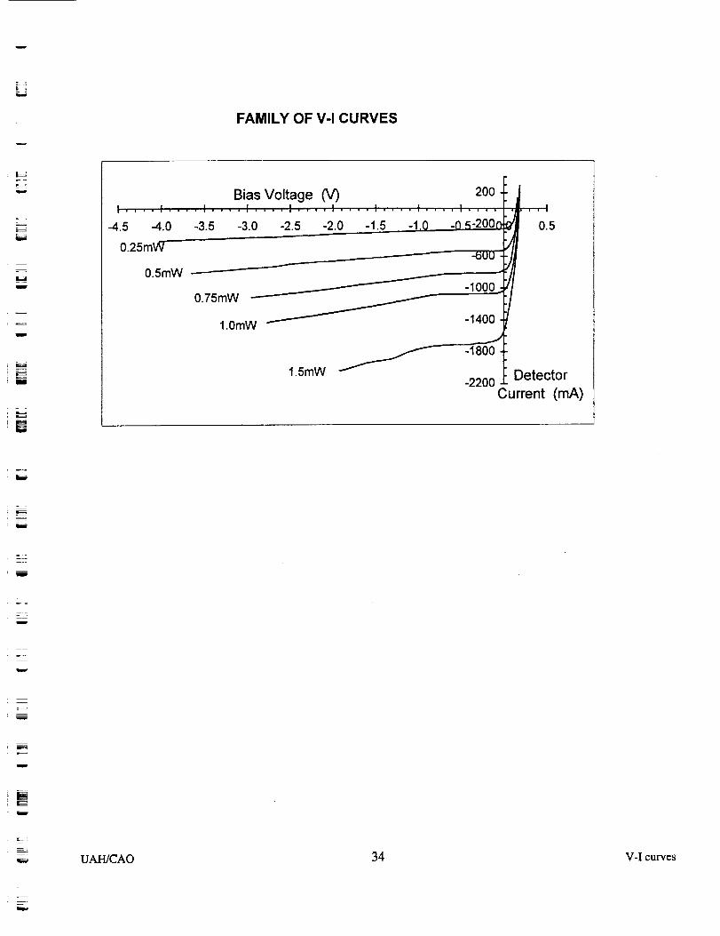
FAMILY OF V-I CURVES
w
I
E
W
W
Bias Voltage (V) 200I .... I .... I .... I .... I .... I .... I .... I .... I ....
-4.5 -4.0 -3.5 -3.0 -2.5 -2.0 -1.5 -1,0 -0 5-200r_
0.25mW
0.5mW-- -1000
0.75mW 1-
1.0mW _ -1400
1.5mW /-2200
, , , I
2_ 0.5
A
Detector
Current (mA)
L
W
w
==
i
w
z
m
--=
i==:
w
UAH/CAO 34 V-I curves
J_
=
L_i
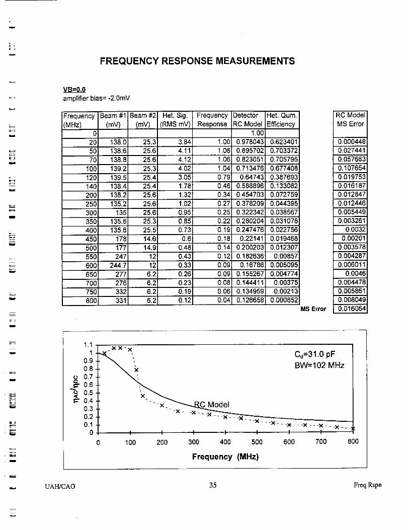
FREQUENCY RESPONSE MEASUREMENTS
= _.
i
w
= =
W
L..z
iil
W
E
_=t
I
VB--0.0
amplifier bias= -2.0mV
Frequency(MHz)
Beam #1
(m_
Beam #2
(mY)
Het. Sig.
(RMS mV)
FrequencyResponse
DetectorRC Model
Het. Qum.
Efficiency0 1.00
20 138.0 25.3 3.84 1.00 0.978043 0.62340150 138.6 25.6 4.11 1.06 0.895702 0.703372
138.8
139.2139.5
7O 25.625.3
25.425.4
100
4.124.023.051.78
120
1.06
1.040.790.46140
0.823051
0.7134760.64743
0.588896138.4
0.7057950.6774080.3876930.133082
200 138.2 25.6 1.32 0.34 0.454703 0.072759250 135.2 25.6 1.02 0.27 0.378209 0.0_395300 135 0.95 0.25 0.322342 0.03856725.6
25.3 0.85350 135.6400 135.6 25.5 0.73450 178 14.6 0.650O 177 O.48550 247
0.2802040.22
14.912 0.43
0.0310780.19 0.247476 0.0227560.18 0.22141 0.0194680.14 0.200203 0.0123070.12 0.182636 0.00857
600 244.7 12 0.33 0.09 0.16786 0.005095650 277 6.2 0.26 0.09 0.155267 0'.004774
700 276 6.2 0.23 0.08 0.144411750 332 6.2 0.19
331 6.2 0.128OO
0.06 0.1349590.1266580.04
0.00375=_,
0.002130.000852
MS Error
RC Model
MS Error
0.0004480.0274410.057663
0.1076540.0197530.0161870.0128470.0124460.0054490.003261
0.0032
0.002010.0035780.0042870.006011
0.00460.0044780.0058610.0080490.016064
w
w
=:=
i
Z
1.11
0.90.8
o 0.70.6
_0.50.40.30.20.1
0
__ Cd=31.0 pF
BW=102 MHz
'-x.. _Model
"-x-- -x____x` --x:::_-:--"_ :-_-_'_I I 1 t' I I I
0 1O0 200 300 400 500 600 700 800
Frequency (MHz)
w UAH/CAO 35 Freq Rspn
L
= :
w
=
w
L
= =
W
= =
W
W
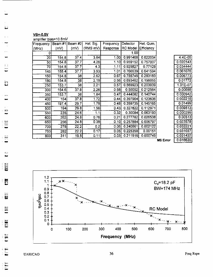
VB=-0.SV
amplifier bias=10.8mVFrequency Beam#1 Beam #2 Het. Sig Frequency Detector Het. Qum.(MHz) (mV) (mV) (RMS mV) Response RC Model Efficiency
0 1.0020 154.8 37.4 3.84 1.00 0.991468 0.62203450 154.8 37.7 4.26 1.10 0.959152 0.75700770 154.8 37.7 4.3 1.11 0.925827 0.77129
145 155.4 37.7 3.93 1.01 0.766539 0.641594150 154.8 38 2.62180 154.8 38 2.181250 153.7 38 2.21
300 154.6 37.8 2.26350 153.7 38 1.84
37.8 1.72400 154450 197.4 29.7 1.78500 194 29.8 1.56i
550 235 24.6 1.124.8262 0.76600
650 256 24.8 0.38700 278 22.2 0.2750 282 22.2 0.17!
19.58OO 311 0.11
0.67 0.755745 0.2831830.56 0.693462 "0.196055
0.57 0.569923 0.2030390.58 0.50052 0.2125640.47 0.444082 0.140744
0.3979040.44 0.1236360.48 0.359735 0.145165
0.43 0.327822 0.112971....... 0.32 0.30084 0.063193
0.21 0.277782 0.0265380.10 0.257884 0.0067970.06 0.240561 0.0021220.05 0.225358 0.00151
0.2119160.03 0.000749MS Error
4.4E-050.0201430.0344440.0610760.0067730.01772
1.01E-070.00688
0.0009420.0022160.01499
0.0095130.0002990.00513
0.023578
0.0332210.0310370.0314320.016635
w_
w
w
w
w
w
=
1.21.1
10.90.80.70.6
"_ 0.5
t=" 0.40.30.20.1
0
0
"_- - "'x C_=18.2 pF_ ', BW=174 MHz
odel
"X.
--X - - -X - - -I I I I I I I
100 200 300 400 500 600 700 800
Frequency (MHz)
Ii UAH/CAO 36 Freq Rspn
w
w
w
w
zw
w
w
W
w
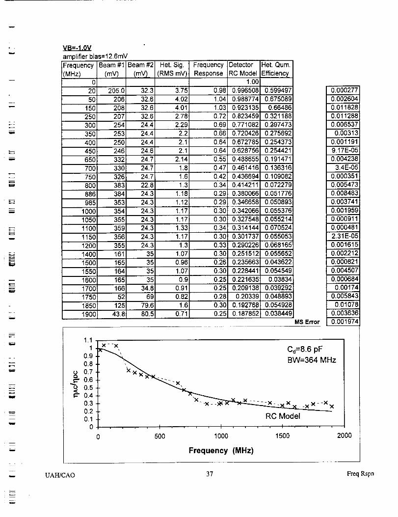
Vl_=-I .OVamplifier bias=12.6mV
Frequency Beam#1 Beam #2 Het. Sig. Frequency Detector Het. Qum.(MHz) (mV) (mV) (RMS mV) Response RC Model Efficiency
0 1.00
205.0
35O
32.3 3.75 0.98 0.996508 0.5994972O50 206 32.6 4.02 1.04 0.988774 0.675089
150 208 32.6 4.01 1.03 0.923135 0.66486250 207 32.6 2.78 0.72 0.823459 0.321188300 254 24.4 2.29 0.69 0.771082 0.297473
253 24.4 2.2 0.720426 0.2756920.66o.6 ,400 250 24.4 2.1 0.672785 0.254373
450 246 24.6 2.1 0.64"0.628756 0.254421
650 332 24.7 2.14 0.55 0.488655 0.191471330326
7007508OO886
383
384985 353
1000 3541050 355
1100 3591150 356
355161165164165
1200
24.724.722.824.324.3
24.324.324.324.324.3
3535
3535
34.8
1400
1.81.61.3
1.181.121.171.17
1.331.171.3
1.070.961.07
0.90.91
15001 5o16001700
0.47
0.420.340.290.290.30
0.300.34
0.300.33
0.300.260.30
0.250.250.280.30
0.461416
166
0.4366940.4142110.3800660.3466580.342066O.327548'0.314144
0.3017370.2902260.2515120.2356630.228441
0.2216350.209138
0.20339
0.136316
1750 52 69 0.82
1850 125 79.6 1.61900 43.8 80.5 0.71!
0.109082
0.0722790.0517760.0508930.0553760.0552140.070524
0.0550530.0681650.0556520.0436220.054549
0.038340.0392920.048893
0.192768 0.0549280.25 0.187852 0.038449
MS Error
1.1
0.0002770.0026040.0118280.0112880.006537
0.00313
0.0011919.17E-050.004238
3.4E-050.0003510.0054730.008483
0.0037410.0019590.0009110.0004812.31E-050.0016150.0022120.000821
0.00450710.000684:0.00174
0.0058430.01078
0.003636'
0.001974
W
!
N
-!
w
10.90.8
o 0.70.60.5
_" 0.40.30.20.1
0
0d=8.6 pF
BW=364 MHz
X._x__x x x ..... x_. x __xx--Xx
RC Model
i i i
0 500 1000 1500 2000
Frequency (MHz)
t
= :
UAH/CAO 37 Freq Rspn
w
I
-/
I
w
= .
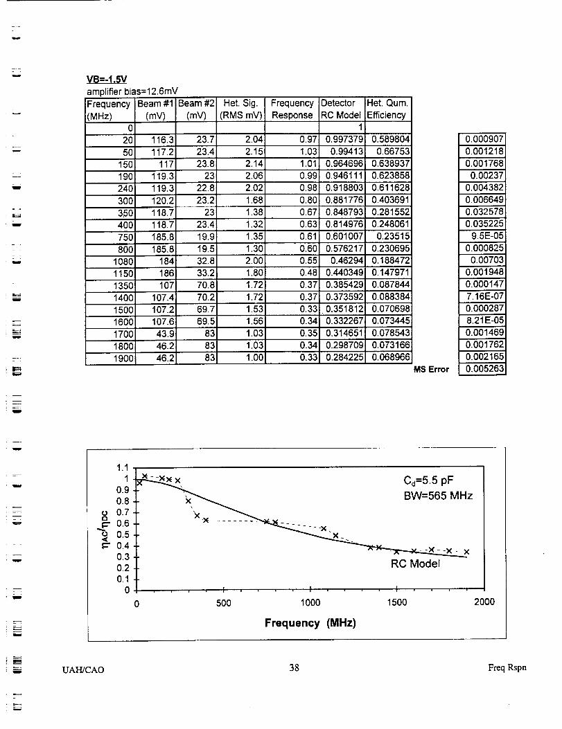
VI_=-I.svamplifier bias=12.6mV
Frequency(MHz)
Beam #1
(m_
Beam #2
(m_Het. Sig.
(RMS mY)FrequencyResponse
DetectorRC Model
Het. Qum.
Efficiency0
20 116.3 23.7 2.04 0.97 0.997379 0.58980450 117.2 23.4 2.15 1.03 0.99413 0.66753
150 117 23.8 2.14 1.01 0.964696 0.638937190 119.3 23 2.06 0.99 0.946111 0.623858240 119.3 22.8 2.02 0.98 0.918803 0.611628
300 120.2 23.2 1.683_0 118.7 23 1.38400 118.7 23.4 1.32
19.919.5
750 1.35
1.30185.8185.88OO
1080 184 32.8 2.001150 186 33.2 1.801350 107 70.8 1.72
107.414001500
1.721.53107.2
0.80 0.881776 0.4036910.848793 0.281552
0.2480610.670.63
0.61
0.600.55
0.8149760.6010070.576217
70.2
0.46294
0.235150.2306950.188472
0.48 0.440349 0.1479710.37 0.385429 0.087844
0.373592
69.7
0.370.33 0.351812
0.332267
0.0883840.070698
1600 107.6 69.5 1.56 0.34 0.0734451700 43.9 83 1.03 0.35 0.314651 0.0785431800 46.2 83 1.03 0.34 0.298709 0.073166
1.0083 0.3346.21900 0.284225 0.068966MS Error
0.0009070.0012180.001768
0.002370.004382
0.0066490.0325780.035225
9.5E-050.000825
0.007030.0019480.0001477.16E-070.0002878.21E-05
0.0014690.0017620.0021650.005263
w
i
I
w
I
!
1.11
0.90.8
0.70.6
E 0.5_" 0.4
0.30.20.1
0
Cd=5.5 pF
k BW=565 MHz
...... -X.x_
RC Model
I I , I
0 500 1000 1500 20O0
Frequency (MHz)
UAFUCAO 38 Freq Rspn
w
z :
w
= :
w
w
= =
w
w
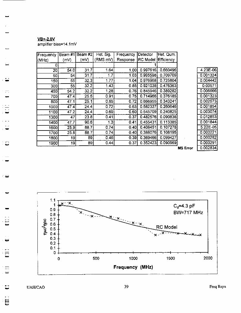
VB=-2.0V
amplifier bias=14.1 mV
Frequency Beam #1 Beam #2 Het. Sig. Frequency Detector Het. Qum.
(MHz) (mV) (mV) (RMS mV) Response RC Model Efficiency0 1
20 54.0 31.7 1.64 1.00 0.997616 0.660496
50 54 31.7 1,7 1.03 0.995598 0.709709150 55 32.3 1.77 1.04 0.976968 0.725804300 55 32.2 1.43 0.85 0.921038 0.476363
450 54.2 32.2 1.28 0.76 0.845946 0.389282700 47.4 25.5 0.91 0.75 0.714966 0,376i'8'5
800 47.1 25.1 0.85 0.72 0.666955 0.3432411000 47.4 24.4 0.72 0.63 0.582337 0.2606461100 47.2 24.4 0,69 0.60 0.545709 0.2408251300 47 23.8 0.41 0.37 0.482576 0.0908381400 47.7 90.6 1.3 0.41 0.455431 0.1133851600 25.9 88.7 0.74 0.40 0.408451 0,1072781700 25.8 88.7 0.74 0.40 0.388076 0.108195
1800 19 89 0.46 0.39 0.369466 0.0994271900 19 89 0.44 0.37 0.352423 0.090969
MS Error
4.23E-060.0013240.004442
0.005710.006666
0.0013230.0025730.0018540.0030740.0128530.0018445.22E-050.0002210.000282
0.0002910.002834
w
W
W
w
1.11
0.90.8
o 0.7c= 0.6
_<_. 0.50.40.30.20.1
0
"_x Ca=4.3 pF"'x. BW=717 MHz
I I .... I
500 1000 1500
Frequency (MHz)
2000
UAH/CAO 39 Freq Rspn
= ,
r_
¢,==_
L
E_
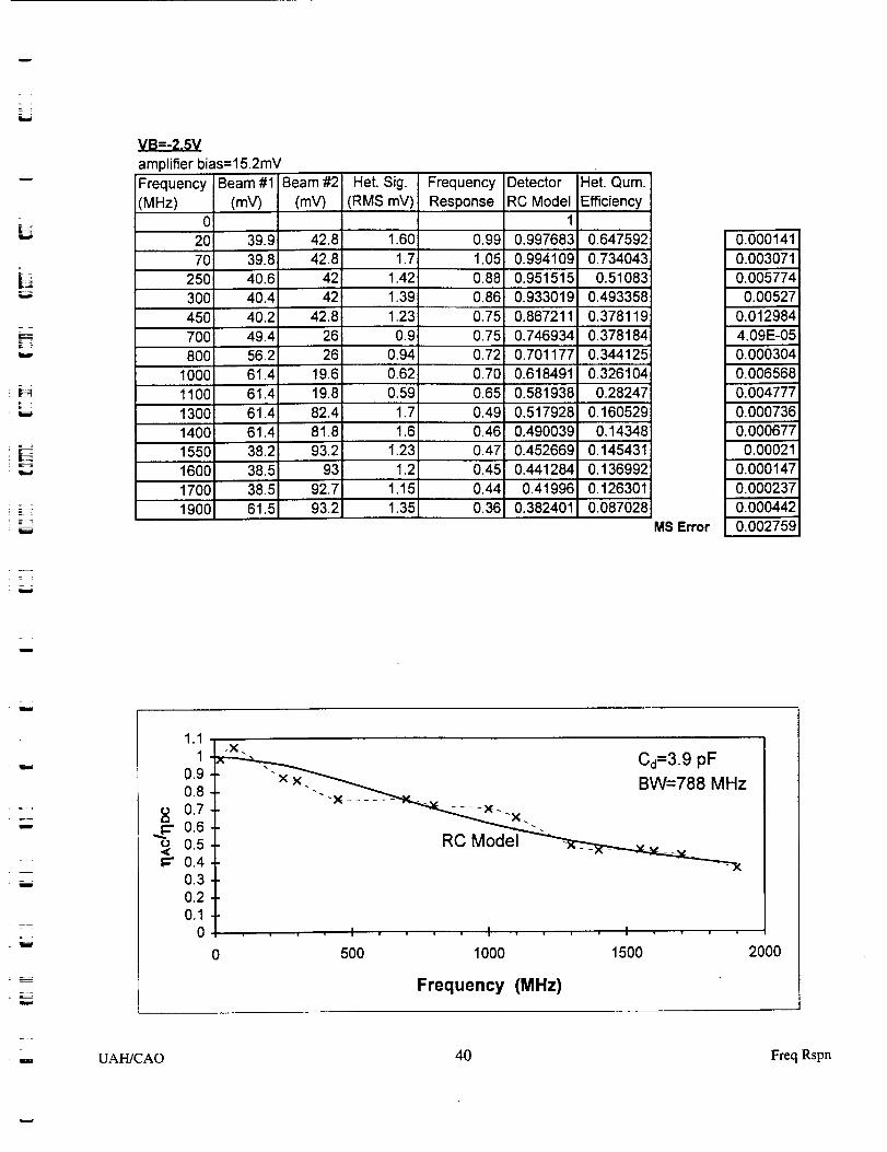
VB=-2.SV
amplifier bias=15.2mVFrequency(MHz)
Beam #1
(mY)
Beam #2
(mY) ..
Het. Sig.(RMS mV)
rw
Frequency
Response
DetectorRC Model
Het. Qum.
Efficiency0
20 39.9 42.8 1.60 0.99 0.997683 0.64759270 39.8 42.8 1.7 1.05 0.994109 0.734043
250 40.6 42 1.42 0.88 0.951515 0.510830.86 0.933019 0.493358
'01'75 0.867211 0.378119
0.75 0.746934
300 40.4 42 1.39
450 40.2 42.8 1.230.378184700 49.4 26 0.9
800 56.2 26 0.941000 61.4 19.6 0.62
0.72 0.701177 0.3441250.70 0.618491 0.326104
1100 61.4 19.8 0.59 0.65 0.581938 0.28247
1300 61.4 82.4 1.7 0.49 0.517928 0.1605291400 61.4 81.8 1.6 0.46 0.490039 0.14348
1.2393.2 0.4526690.47
61.5
0.1454311550 38.21600 38.5 93 1.2 0.45 0.441284 0.1369921700 38.5 92.7 1.15 0.44 0.41996 0.1263011900 93.2 1.35 0.36 0.382401 0.087028
MS Error
0.0001410.0030710.005774
0.005270.0129844.09E-050.0003040.0065680.004777
0.00O7360.000677
0.000210.0001470.0002370.0004420.002759
zw
w
ii
w
W
1.11
0.90.8
o 0.7
t=" 0.40.30.20.1
0
"x " Cd=3.9 pF
"xx_ -_ BW=788 MHz
5OO 1000 1500
Frequency (MHz)
2000
.= _
w UAH/CAO 40 Freq Rspn
w
w
i===;
w
, [,-_E_
5=
w
z
w
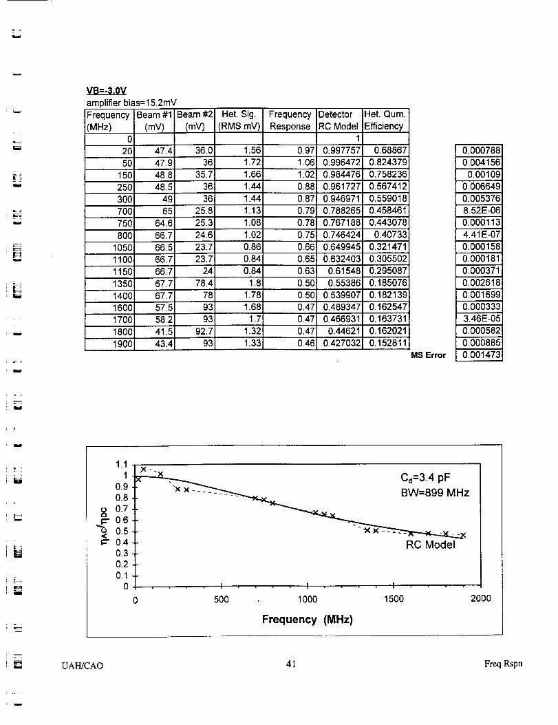
VB=-3,0V
amplifier bias=15.2mV
Frequency Beam #1 Beam#2 Het. Sig Frequency Detector Het. Qum.
(MHz) (mV) (mY) (RMS mV) Response RC Model Efficiency0 1
20 47.4 36.0 1.56 0.97 0.997757 0.68867
50 47.9 36 1.72 1.06 0.996472 0.824379
150 48.8 35.7 1.66 1.02 0.984476 0.758236
250 48.5 36 1.44 0.88 0.961727 0.567412
300 49 36 1.44 0.87 0.946971 0.559018
700 65 25.8 1.13 0.79 0.788265 0.458461
750 64.6 25.3 1.08 0.78 0.767188 0.443078
800 66.7 24.6 1.02 0.75 0.746424 0.40733
1050 66.5 23.7 0.86 0.66 0.649945 0.321471
1100 66.7 23.7 0.84 0.65 0.632403 0.305502
1150 66.7 24 0.84 0.63 0.61548 0.295087
1350 67.7 78.4 1.8 0.50 0.55386 0.185076
1400 67.7 78 1.78 0.50 0.539907 0.182139
1600 57.5 93 1.68 0.47 0.489347 0.162547
1700 58.2 93 1.7 0.47 0.466931 0.163731
1800 41.5 92.7 1.32 0.47 0.44621 0.162021
1900 43.4 93 1.33 0.46 0.427032 0.152811
MS Error
0.000788
0.004156
0.00109
0.006649
0.005376
8.52E-06
0.000113
4.41E-07
0.000158
0.000181
0.000371
0.002618
0.001699
0.0003331i
3.46E-05
0.000582
0.000885
0.001473
L_
!
1.1
1
0.9
0.8
0.70.6
0.50.4
0.3
0.2
0.1
0
_-" C_=3.4 pF
BW=899 MHz
RC Model
0
I I .... I
500 1000 1500
Frequency (MHz)
2000
UAH/CAO 41 Freq Rspn
w
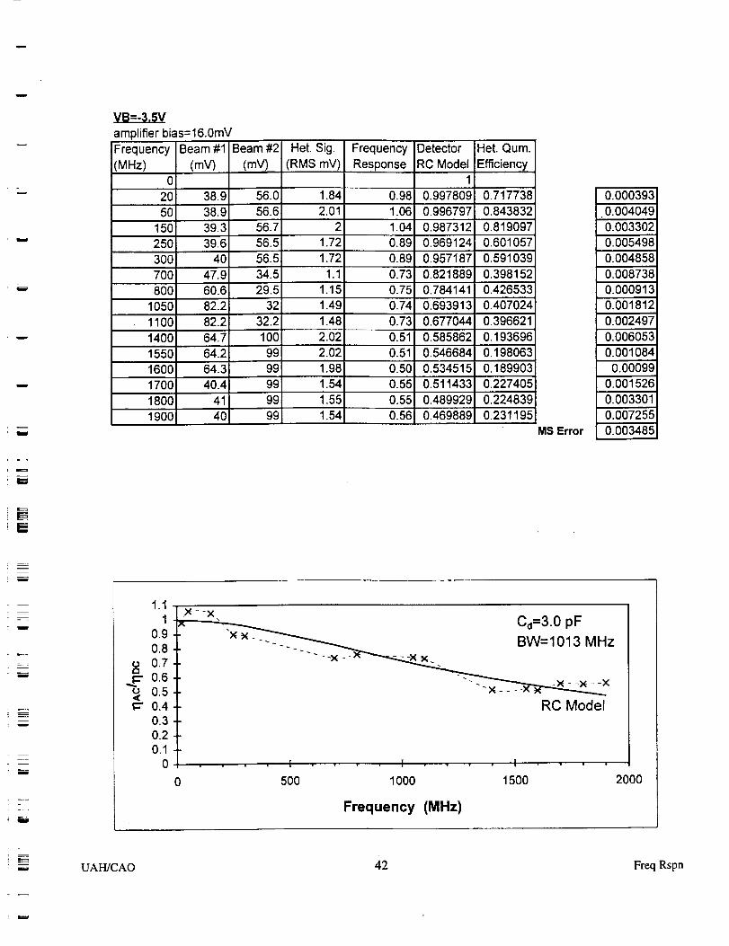
VB=-3.5V
amplifier bias=16.0mV
Frequency Beam #1 Beam #2(VHz) (mV) (mV)
020 38.9 56.050 38.9 56.6
150 39.3 56.7250 39.6 56.5
3O0 4O 56.57OO 47.9 34.5800 60.6 29.5
1050 82.2 321100 82.2 32.21400 64.7 100
1550 64.2 991600 64.3 991700 40.4 991800 41 991900 40 99
Het. Sig. Frequency Detector Het. Qum.
!(RMS mV) ResPonse RC Model Efficiency1
1.84 0.98 0.997809 0.717738
2.01 1.06 0.996797 0.8438322 1104 0.987312 0.819097
1.72 0.89 0.969124 0.6010571.72 0.89
0.731.10.9571870.821889
1.15
0.5910390.3981520.4265330.75 0.784141
1.49 0.74 0.693913 0.4070241.48 0.73 0.677044 0.396621
2.02 0.51 0.585862 0.1936962.02 0.51 0.546684 0.1980631.98 0.50 0.534515 0.1899031.54 0.55 0.511433 0.227405
0.4899290.469889
0.551.551.54 0.56
O.2248390.231195
MS Error
0.0003930.0040490.003302
0.0054980.0048580.0087380.0009130.0018120.0024970.006053
0.0010840.00099
0.0015260.0033010.0072550.003485
w
!
==
1.11
0.90.8
u 0.7
t=" 0.40.30.20.1
0
,_-_X
,_ _ Cd=3.0 pF"x x__ BW=1013 MHz
RC Model
I • I • I
500 1000 1500
Frequency (MHz)
2000
UAH/CAO 42 Freq Rspn

L
w
z
L
w
r_
m
m
_.._Aw
;==
VB=-4.0V
amplifier bias=17.2mVFrequency(MHz)
0
Beam #1
(mV)
1880
Beam #2
(mV)
37.1
Het. Sig.(RMS mV)
FrequencyResponse
DetectorRC Model
Het. Qum.
Efficiency
20 59.7 43.1 2.02 0.98 0.997821 0.76023250 59.9 43.2 2.2 '1.06 0.996872 0.89408
150 60.3 43 2.1 1.01 0.987971 0.813343200 60.3 43 2.02 0.97 0.980374 0.752554
300 60.5 43.3 1.84 0.88 0.959597 0.614383450 59.7 43.8 1.78 0.85 0.917286 0.57478700 63 32 1.35 0.83 0.830295 0.551407820 62.4 32.8 1.35 0.82 0.786417 0.530074
1080 53.8 26.8 0.93 0.80 0.695386 0.5048311250 51.5 24.7 0.64 0.64 0.64i487 0.32654
1330 53.7 55.5 1.36 0.59 0.617926 0.2713431350 51.7 24.7 0.58 0.58 0.612218 0.266629
1400 63.5 24.7 0.65 0.56 0.598266 0.2495261500 64.3 24.7 0.61 0.52 0.571702 0.2160281600 65.2 24.9 0.61 0.51 0.546865 0.2064711700 66.7 25 0.62 0.51 0.523666 0.204181
104.5 1.41 0.54 0.485712 0.234695MS Error
0.0003380.0042620.00063
3.48E-05
0.0062590.0043111.47E-050.000987
0.0105561.72E-070.0010750.0010360.001380.00246
0.0013280.0002590.00342
0.002256
zw
i
w
----
w
L_w
w
w
1.11
0.90.8
._ot="0.70.6
0.5t=" 0.4
0.30.20.1
0
Cd=2.9 pF
x_ ___ _W=1047 MHz
RC Model
I I !
500 1000 1500
Frequency (MHz)
2000
w UAH/CAO 43 Freq Rspn
w
= ;
w
w
w
w
w
m
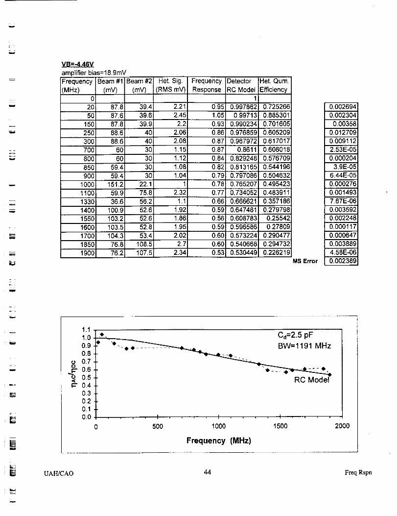
VB=-4.46V
amplifier bias=l 8.9mY
Frequency Beam #1 Beam #2 Het. Sig. Frequency Detector Het. Qum.(MHz) (mY) (mV) (RMS mY) Response RC Model Efficiency
0 12050
150
2503OO70080O
87.887.687.888.6
88.66060
39.439.639.9
4O4O3O3O3O
2.212.452.2
2.06
2.081.151.121.08
0.95
1.050.93
0.860.870.87
0.840.82
0.9978620.99713
0.9902340.9768590.967972
0.8611
0.829248O.813165
0.725266
0.8853010.7016050.6052090.6170170.608018
0.57670910.544196850 59.4
900 59.4 30 1.04 0.79 0.797086 0.5046321
1000 151.2 22.1 1 0.78 0.765207 0.4954231100 59.9 75.8 2.32 0.77 0.734052 0.483911
36.6 56.2 1.1 0.66 0.666621 0.35718613301400 100.9 52.6 1.921550 103.2 52.6 1.861600 103.5 52.8 1.95
76.2
0.59 0.647481 0.2797980.56 0.608783 0.25542
0.59 0.596586 0.278090.5732240.60 0.2904771700 104.3 53.4 2,02
1850 76.8 108.5 2.71900 107.5 2.34 0.53
n,,
0.60 0.540668 0.2947320.530449 0.226219
MS Error
0.0026940.002304
0.00358
0.0127090.0091122.53E-050.000204
3.9E-056.44E-05
0.0002760.0014937.67E-060.0035920.0022480.000117
0.0006470.0038894.58E-060.002389
.===w
w
E=
--=r--=
w
L
1.1
1.0 _ Cd=2.5 pF0.9 Jr" "--..__ __ BW= 1191 MHz0.8 • _ - --e._
0.60.5 RC
_" 0'4 I
0.30.20.10.0 I I w
0 500 1000 1500
Frequency (MHz)
2000
UAH/CAO 44 Freq Rspn
=
Detector Capacitance
w
r
w
w
r_
w
VB (V) C,j (pF)
0.0 31.0
0.5 18.2
1.0 8.6
1.5 5.5
2.0 4.3
2.5 3.9
3.0 3.4
3.5 3.0
4.0 2.9
4.5 2.5
w
E_
w
m
m
w
w
35.0
1,4.30.0
25.0
"_ 20.0
15.0tO
10.0
5.0
0.0 ' I ' I ' t
0o0 1.0 2.0 3.0
¢ • ¢
' t
4.0
I
Bias Voltage (V)
5.0
i
w
r_=
= UAH/CAO 45 Freq Rspn
u
w
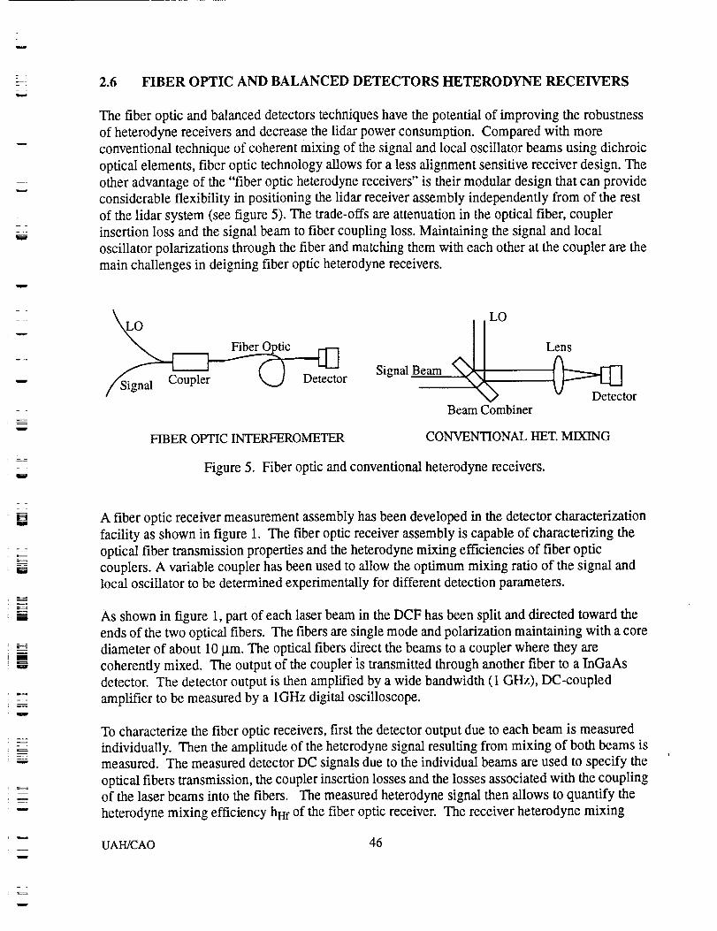
2.6 FIBER OPTIC AND BALANCED DETECTORS HETERODYNE RECEIVERS
The fiber optic and balanced detectors techniques have the potential of improving the robustness
of heterodyne receivers and decrease the lidar power consumption. Compared with more
conventional technique of coherent mixing of the signal and local oscillator beams using dichroic
optical elements, fiber optic technology allows for a less alignment sensitive receiver design. The
other advantage of the "fiber optic heterodyne receivers" is their modular design that can provide
considerable flexibility in positioning the lidar receiver assembly independently from of the rest
of the lidar system (see figure 5). The trade-offs are attenuation in the optical fiber, coupler
insertion loss and the signal beam to fiber coupling loss. Maintaining the signal and local
oscillator polarizations through the fiber and matching them with each other at the coupler are the
main challenges in deigning fiber optic heterodyne receivers.
/Signal Coupler k,._J Detector
Signal Beam LO
Beam Combiner
Lens
Detector
FIBER OPTIC INTERFEROMETER CONVENTIONAL HET. MIXING
Figure 5. Fiber optic and conventional heterodyne receivers.
W
i
A fiber optic receiver measurement assembly has been developed in the detector characterization
facility as shown in figure 1. The fiber optic receiver assembly is capable of characterizing the
optical fiber transmission properties and the heterodyne mixing efficiencies of fiber optic
couplers. A variable coupler has been used to allow the optimum mixing ratio of the signal and
local oscillator to be determined experimentally for different detection parameters.
As shown in figure 1, part of each laser beam in the DCF has been split and directed toward the
ends of the two optical fibers. The fibers are single mode and polarization maintaining with a core
diameter of about 10 I.tm. The optical fibers direct the beams to a coupler where they are
coherently mixed. The output of the coupler is transmitted through another fiber to a InGaAs
detector. The detector output is then amplified by a wide bandwidth (1 GHz), DC-coupled
amplifier to be measured by a 1GHz digital oscilloscope.
To characterize the fiber optic receivers, first the detector output due to each beam is measured
individually. Then the amplitude of the heterodyne signal resulting from mixing of both beams is
measured. The measured detector DC signals due to the individual beams are used to specify the
optical fibers transmission, the coupler insertion losses and the losses associated with the couplingof the laser beams into the fibers. The measured heterodyne signal then allows to quantify the
heterodyne mixing efficiency hHf of the fiber optic receiver. The receiver heterodyne mixing
UAH/CAO 46
F_
w
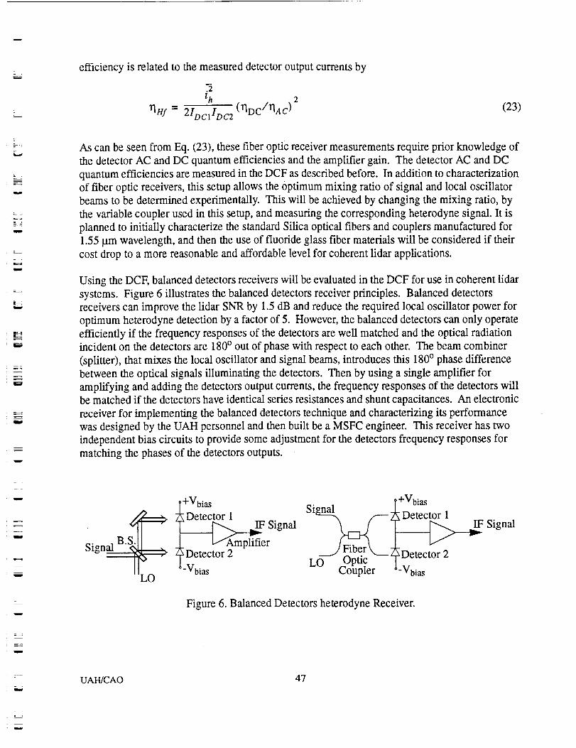
w
efficiency is related to the measured detector output currents by
_h
"qHf - 2IDcIlDc 2 (qDC/qAC)(23)
g_,
r_w
_=_
_=
As can be seen from Eq. (23), these fiber optic receiver measurements require prior knowledge of
the detector AC and DC quantum efficiencies and the amplifier gain. The detector AC and DC
quantum efficiencies are measured in the DCF as described before. In addition to characterization
of fiber optic receivers, this setup allows the Optimum mixing ratio of signal and local oscillator
beams to be determined experimentally. This will be achieved by changing the mixing ratio, by
the variable coupler used in this setup, and measuring the corresponding heterodyne signal. It is
planned to initially characterize the standard Silica optical fibers and couplers manufactured for
1.55 pan wavelength, and then the use of fluoride glass fiber materials will be considered if their
cost drop to a more reasonable and affordable level for coherent lidar applications.
Using the DCF, balanced detectors receivers will be evaluated in the DCF for use in coherent lidar
systems. Figure 6 illustrates the balanced detectors receiver principles. Balanced detectors
receivers can improve the lidar SNR by 1.5 dB and reduce the required local oscillator power for
optimum heterodyne detection by a factor of 5. However, the balanced detectors can only operate
efficiently if the frequency responses of the detectors are well matched and the optical radiation
incident on the detectors are 180 ° out of phase with respect to each other. The beam combiner
(splitter), that mixes the local oscillator and signal beams, introduces this 180 ° phase difference
between the optical signals illuminating the detectors. Then by using a single amplifier for
amplifying and adding the detectors output currents, the frequency responses of the detectors will
be matched if the detectors have identical series resistances and shunt capacitances. An electronic
receiver for implementing the balanced detectors technique and characterizing its performance
was designed by the UAH personnel and then built be a MSFC engineer. This receiver has two
independent bias circuits to provide some adjustment for the detectors frequency responses for
matching the phases of the detectors outputs.
W
w
+Vbias _ IDetector l Si
_ Signal _it-f AmplifierDetector 2
_Vbias LO OpticCoupler
+Vbias
Detector 1
_ Signal
_,Detector 2
'-Vbias
Figure 6. Balanced Detectors heterodyne Receiver.
UAH]CAO 47
w
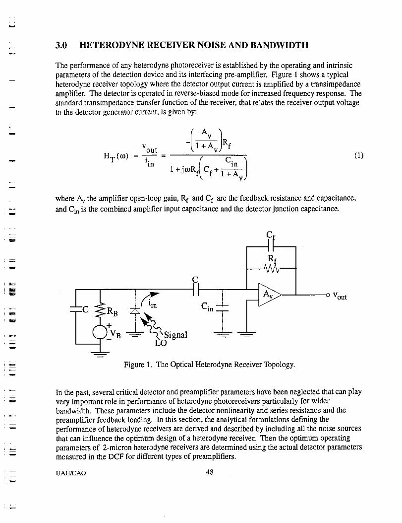
w
w
w
w
w
3.0 HETERODYNE RECEIVER NOISE AND BANDWIDTH
The performance of any heterodyne photoreceiver is established by the operating and intrinsic
parameters of the detection device and its interfacing pre-amplifier. Figure 1 shows a typical
heterodyne receiver topology where the detector output current is amplified by a transimpedance
amplifier. The detector is operated in reverse-biased mode for increased frequency response. The
standard transimpedance transfer function of the receiver, that relates the receiver output voltage
to the detector generator current, is given by:
Av )RfVou t - 1 +A v
- (1)
HT(C°) - iin ( Cin ]l+jcoRf Cf+ 1 +A v
where A v the amplifier open-loop gain, Rf and Cf are the feedback resistance and capacitance,
and Cin is the combined amplifier input capacitance and the detector junction capacitance.
w
E_
i
_s
w
Figure 1. The Optical Heterodyne Receiver Topology.
o Vou t
u
m
mw
In the past, several critical detector and preamplifier parameters have been neglected that can play
very important role in performance of heterodyne photoreceivers particularly for wider
bandwidth. These parameters include the detector nonlinearity and series resistance and the
preamplifier feedback loading. In this section, the analytical formulations defining the
performance of heterodyne receivers are derived and described by including all the noise sources
that can influence the optimum design of a heterodyne receiver. Then the optimum operating
parameters of 2-micron heterodyne receivers are determined using the actual detector parameters
measured in the DCF for different types of preamplifiers.
UAH/CAO 48
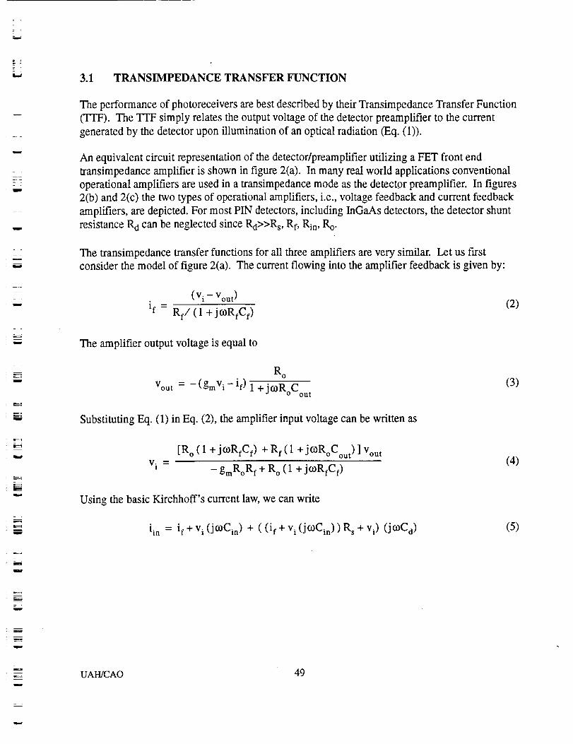
w
w
w i
m
w
3.1 TRANSIMPEDANCE TRANSFER FUNCTION
The performance of photoreceivers are best described by their Transimpedance Transfer Function
(TTF). The TTF simply relates the output voltage of the detector preamplifier to the current
generated by the detector upon illumination of an optical radiation (Eq. (1)).
An equivalent circuit representation of the detector/preamplifier utilizing a FET front end
transimpedance amplifier is shown in figure 2(a). In many real world applications conventional
operational amplifiers are used in a transimpedance mode as the detector preamplifier. In figures
2(b) and 2(c) the two types of operational amplifiers, i.e., voltage feedback and current feedback
amplifiers, are depicted. For most PIN detectors, including InGaAs detectors, the detector shunt
resistance R d can be neglected since Rd>>R s, Rf, Rin, R o.
The transimpedance transfer functions for all three amplifiers are very similar. Let us first
consider the model of figure 2(a). The current flowing into the amplifier feedback is given by:
(V i -- Vout)
if = Rf/(1 + jcoRfCf)(2)
The amplifier output voltage is equal to
R o
You t = - (gmVi - if) 1 +j03RoCou t(3)
Substituting Eq. (1) in Eq. (2), the amplifier input voltage can be written as
[R o ( 1 + j _RfCf) + R e ( 1 + j O_RoCout) ] Yout
Vi = - gmRoRf + R o ( 1 + j0_RfCf)(4)
Using the basic Kirchhoff's current law, we can write
iin = if + Vi (j_Cin) + ( (if + v i (J_Cin) ) R s + vi) (j0_Cd) (5)
w
UAH/CAO 49
w
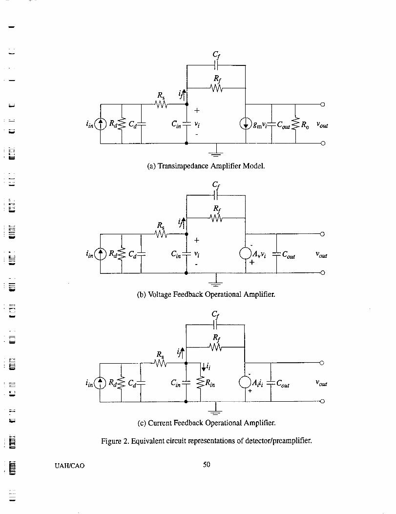
=
w
E
L_
s T
w
F-
W
B
w
= :
w
w
= :
i
=
u
w
k_
r_
e S
clIt
q
+
Ci n -- v i
_1_
_'IgmVi_C°utl R°
(a) Transimpedance Amplifier Model.
o
Vout
©
clIt
gs _ I
vi
w _2_
)Avv i+
(b) Voltage Feedback Operational Amplifier.
Lco ©
- ut Vout0
iin_ ed I Cd_
_fi
Cin-- _Rin
_L_(c) Current Feedback Operational Amplifier.
(_+ Aiii _ Cout
Figure 2. Equivalent circuit representations of detector/preamplifier.
o
V out
©
UAH/CAO 50
w
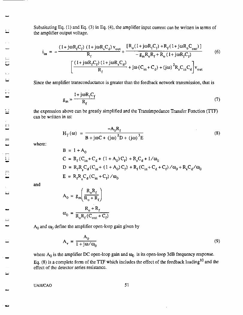
=,w
w
w
===
w
L =
w
_ .
m
w
_w
Substituting Eq. (1) and Eq. (3) in Eq. (4), the amplifier input current can be written in terms of
the amplifier output voltage.
(l+j0_RfCf) (l+j_RsCd) Vou t [Ro(l+jc.oRfCf) +Rf(l+jo)RoCout)]
iin = - Rf + (6)- gmRoRf + R o ( 1+ j_RfCf)
( 1+ j o)RfCf) ( 1+ j 0)RsCd) ]Re +j0) (Cin + Cd) + (j0_) 2RsCinC d Yout
Since the amplifier transconductance is greater than the feedback network transmission, that is
1 + j o_RfCf
gm >> Rf (7)
the expression above can be greatly simplified and the Transimpedance Transfer Function (TIT)can be written in as:
where:
and
-AoR fH T (co) = (8)
B +jo_C+ (jo_)ZD + (j_)3E
B = I+A o
C = Rf(Cin+Cd + (1 +Ao)Cf) +RsCd+ 1/_ o
D = RfRsC d (Cin + (1 + Ao) Cf) + Rf (Cin + C d + Cf)/(o 0 + RsCd/O 0
E = RfRsC d (Cin + Cf)/0,) 0
( RoRf /
ko : gm_R._'_Rf)
030
R o + Rf
RoR f (Cou t + Cf)
A o and o)o define the amplifier open-loop gain given by
m o
Av - 1 + j_/co o (9)
where A o is the amplifier DC open-loop gain and _ is its open-loop 3dB frequency response.10
Eq. (8) is a complete form of the TTF which includes the effect of the feedback loading and theeffect of the detector series resistance.
UAH/CAO 51
t._
!
w
w
Similarly, the TFF can be obtained for voltage and current feedback operational amplifiers
operating in transimpedance mode. For the Voltage Feedback (VF) operational amplifier, shown
in figure l(b), the TIT is basically identical to Eq. (8). The only differences are the expressions
for the open-loop gain and 3 dB frequency response (A 0 and oh3). For the VF operational
amplifier, A o and o.b are usually provided by the manufacturer.
The TIT for CF operational amplifier is also similar to Eq.(8). Using figure l(c) and theKirchhoff's current law, the detector current can be written as
iin = (if+ i i +j0_Cinii ) (1 +jORsCd) +jOCdRini i (10)
Using the equality Vout=-Ziii and after some simple algebraic manipulations, the TIT for CF
operational amplifier can be written in the same form as Eq.(8) but with different coefficients in
the denominator. For CF operational amplifier, the coefficients in the denominator are given by:
B = 1 + A o + Rf/Rin
C = Rf (Cin't" C d -t- (1 + Ao) Cf) + RsC d ( 1 + A o + Rf/Rin ) + ( 1 + Rf/Rin )/o o
D = RfRsC d (Gin + ( 1 + Ao) Cf) + Rf (Cin+ C d + Cf)/ZO o + RsC d ( 1 + Rf/Rin )/O 0
E = RfRsC d (Cin + Cf)/o o (10)
w
!
i
W
_L
Z o
where A o - Ri n- _, and Z0 is the amplifier open-loop gain.
It should be noted that Z o is the open-loop current gain for a current-controlled voltage source
while for VF operational amplifiers, A o refers to the open-loop voltage gain. For all three types of
amplifiers A o is unit-less. As can be seen for the expressions of Eq.(10), the TIT for the CF
operational amplifier is identical to those of transimpedance and VF operational amplifiers when
Rf >> Rin.
Figure 3 shows the normalized magnitude squared of TIT's for each of the amplifier types using
measured data of a 75 micron diameter detector (see section 2.5) and actual parameters of a VF
operational amplifier, a CF operational amplifier, and a 2 GHz MES_T transimpedance
amplifier (see section 3.5). The effect of the series resistance on the TIT's is clear for wider
bandwidths, or smaller feedback resistances. As shown in figure 3, the detector series resistance
causes the receiver gain to peak and then drop faster with frequency. Figure 3 also illustrates that
the last quantity in the denominator of Eq.(8) has a small effect on the TIT and may be neglected.
This fact is illustrated by setting the quantity E equal to zero in the TTF expression. Neglecting
the third power of frequency in the TrF expression will greatly simplify the receiver noise and
bandwidth analyses.
UAH/CAO 52
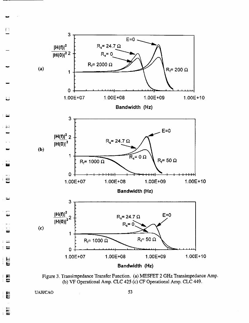
W
w
w
m
r_
ira8
m
E
=
w
(a)
(b)
IH(f)l _
IH(0)122
0
1.00E+07
3
E=0
Rs= 24.7 _ _/RI,
R,=0
! | | | I
1.00E+08 1.00E+09 1.00E+ 10
Bandwidth (Hz)
IH(f)l 2 2
IH(0)I 2
0
E=0
Rs= 24_
Rf=,1000. __.._ Rs-0_ R,.,_=50, ,
i | i ; | i | i | | | | i | i i | | i !| i i i iii = i i .I
1.00E+07 1.00E+08 1.00E+09 1.00E+ 10
Bandwidth (Hz)
3
L_
-- °
=.--w
--=
w
=__
w
(c)
IH(f)122 Rs= 24.7 £Z E=0
:.:1.00E+07 1.00E+08 1.00E+09
i • i ii
1.00E+10
Bandwidth (Hz)
Figure 3. Transimpedance Transfer Function. (a) MESFET 2 GHz Transimpedance Amp.
(b) VF Operational Amp. CLC 425 (c) CF Operational Amp. CLC 449.
UAH/CAO 53
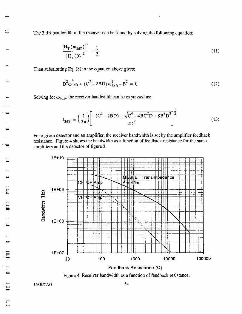
w
The 3 dB bandwidth of the receiver can be found by solving the following equation:
IHT (0)3dB) 1
iH (0)l2 2
Then substituting Eq. (8) in the equation above gives:
2 4D m3da+ (C 2-2BD)oa3dB2 _B 2 = 0
(11)
(12)
i
i
!
m
=
m
Solving for O_3dB, the receiver bandwidth can be expressed as:
f3dB
1
L "}[-(C 2-2BD) + dC4-4BC2D + 8B2D2] _= _,_7_, 2D 2(13)
For a given detector and an amplifier, the receiver bandwidth is set by the amplifier feedback
resistance. Figure 4 shows the bandwidth as a function of feedback resistance for the same
amplifiers and the detector of figure 3.
N
-i-v
r-
"o,w
t--
m
IE+I0
1E+09
1 E+08
1E+07
i
iI!
10 100 1000 10000 100000
UAH/CAO
Feedback Resistance (f_)
Figure 4. Receiver bandwidth as a function of feedback resistance.
54
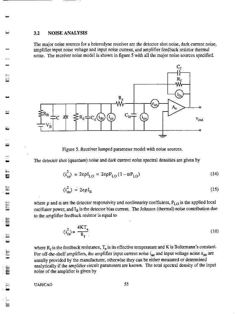
w
w
2 _
m
W
w
J
mw
t
m
3.2 NOISE ANALYSIS
The major noise sources for a heterodyne receiver are the detector shot noise, dark current noise,
amplifier input noise voltage and input noise current, and amplifier feedback resistor thermal
noise. The receiver noise model is shown in figure 5 with all the major noise sources specified.
R S
Wv
_B-_c 2 _Rdlc _A Cin2
+;BTTT T TT
Cf
Vout
Figure 5. Receiver lumped parameter model with noise sources.
The detector shot (quantum) noise and dark current noise spectral densities are given by
(i_n) = 2eplLo = 2ePPLo(1-tXPLo ) (14)
L
z
L_
m
w
m
(i2dn) " 2epI B (15)
where p and {x are the detector responsivity and nonlinearity coefficient, PLO is the applied local
oscillator power, and IB is the detector bias current. The Johnson (thermal) noise contribution due
to the amplifier feedback resistor is equal to
(if2n) = 4 KT eRf (16)
where Rf is the feedback resistance, T e is its effective temperature and K is Boltzmann's constant.
For off-the-shelf amplifiers, the amplifier input current noise ian and input voltage noise ean are
usually provided by the manufacturer, otherwise they can be either measured or determined
analytically if the amplifier circuit parameters are known. The total spectral density of the input
noise of the amplifier is given by
I
UAH/CAO 55
w
w
=:w
w
== =
Ew
W
=--
L_
w
g
°_ °2 °2 °2 ] 1 "dl- j 2_ fRf ( Gin "1- Of) [ 2Si (f) = (lsn) + (ldn) + (lfn) + (lan) + (e]n) Rf(17)
where the last term is the equivalent noise current spectral density of the amplifier input noise
voltage. The total noise referred to the input is obtained by integrating the total current noise
spectral over the normalized receiver TIT magnitude squared.
(iN}= fSi(f) HT(f) 2
o IHT(0)I 2df
Substituting Eq.(17) in Eq.(18), the total noise power is obtained to be
(18)
(i2)= (2ePPLo (1 - C_PLo) + 2epI B +4KTeB e
Rf
.2 (e_n) " HT (f) 2
+ (lan) + W (O)l
+ (2z) 2 (Cin + Cf)2, 2,7 HT(f)_f2df
_'ean) Jo[HT (0)
Using complex contour integration and residue theory, the integrals over the transimpedance
transfer function can be evaluated ]° and expressed as
(19)
o¢
0 HT (0)[ 2df - 4C(20)
i [HT (f) [_f2df B2
oln+(o)l - 16x2CD
where B, C and D are provided in Eqs. (8) and (10). The first integral is proportional to the
receiver bandwidth and the second integral increases almost as bandwidth to the third power.
As noted earlier, the amplifier input current noise and input voltage noise powers (<i2an > and
<e2an>) are usually provided by the manufacturer for more standard VF and CF operational
amplifiers. They may also be measured using standard spectrum analyzers or digitizing
UAH/CAO 56
(21)
Iw
w
u
U
m
W
i
oscilloscopes. The input noise current can be measured by using a large source resistance and the
input noise voltage can be measured by using a small source resistance. However for wide
bandwidth applications which require a bipolar junction transistor or a field effect transistor
amplifier optimized for interaction with a specific detector, it is necessary to express the input
current and voltage noises in terms of the amplifier circuit parameters for optimizing the receiver
design. For a FET front-end amplifier, the input current and voltage noise powers are given
by11.12
.2(lan) = 2elgat e (22)
4KT F 4KT
(e_n) e e_ + (23)gm 2
gmRL
where Igat e is the FET gate current, F is the FET excess noise factor and R L is the FET load
resistance. For a GaAs MESFET amplifier, F is about 1.7. For most FET amplifiers, the FET
channel noise, which is the first term in the voltage noise expression, dominates the other
amplifier noise sources. For a Bipolar front-end amplifier, the input current and voltage noise
powers are given by 11
.2(lan) = 2eI b (24)
(e_n) 2eIc= _ + 4KTerbb, (25)
gm
where I b and Ic are transistor base and collector currents and rbb, is the base-spreading resistance.
3.3 HETERODYNE RECEIVER SIGNAL-TO-NOISE RATIO
The heterodyne signal power, including the effect of the detector nonlinearity, is given by
•
(i_) = 2F 0 [p (1 - 2CtPLo) ] PLOPs (26)
where F o accounts for the signal power reduction due to speckle, turbulence, atmospheric
transmission, misalignment and other systematic losses, and ot is the detector nonlinearity
coefficient. From Eq.(19), the receiver total noise power is equal to
m
UAH/CAO 57
= :
w
=
w
w
7"-J
w
r_w
w
ED
=:=
u
w
w
m
m
2 ( 4KTeBe2 /<IN)= 2ep (1 - _PLo) PLO + 2eld + Rf + (1an) + --_f
2 2 ( B2 )+ (2g) 2(Cin+Cf) (ean) 16_'-CD
(27)
Using Eqs.(26) and (27), the receiver signal Signal-to-Noise Ratio (SNR) can be written in the
following form.
S 292 (1 2t_PLo )2- PLOPsF0
N- ( 4KTe .2
e 9 (1 - CtPLo) PLO + 2eld + R---_ + (1N amp ) )Be
(28)
Where B e is the directly related to the receiver bandwidth and is given by
flH(f)12df B
B_ = _olH(0)l 2 - 4-'C(29)
.2
and (1N,_p)B e accounts for the amplifier total input noise power. From Eq.(27), the amplifier
total noise power per unit frequency can be written as:
.2 .2 (e_n) 2 B
(iNamp) = (1an) +'--_'-f + (Cin +Cf) 2(ean)_(30)
3.4 OPTIMUM LOCAL OSCILLATOR POWER LEVEL
The optimum local oscillator power can be obtained by setting the derivative of the SNR equation
(28) to zero and solve for PLO 5, that is
d(S/N) _ 0 (31)dPLo
After some simple mathematical manipulation, Eq.(31) simplifies to:
2 3 _6ep_p20 .2 .24e9°_ PLO - 60_(1N.mp)PLo + (1N..v) = 0(32)
By numerical evaluation of above equation, the optimum local oscillator power can be obtained
UAI-I/CAO 58
w
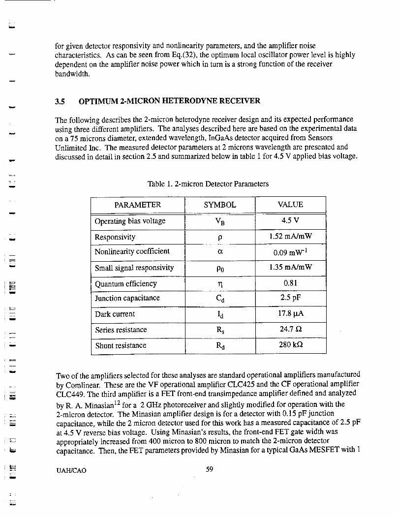
w
for given detector responsivity and nonlinearity parameters, and the amplifier noise
characteristics. As can be seen from Eq.(32), the optimum local oscillator power level is highly
dependent on the amplifier noise power which in turn is a strong function of the receiver
bandwidth.
w
w
3.5 OPTIMUM 2-MICRON HETERODYNE RECEIVER
The following describes the 2-micron heterodyne receiver design and its expected performance
using three different amplifiers. The analyses described here are based on the experimental data
on a 75 microns diameter, extended wavelength, InGaAs detector acquired from Sensors
Unlimited Inc. The measured detector parameters at 2 microns wavelength are presented and
discussed in detail in section 2.5 and summarized below in table 1 for 4.5 V applied bias voltage.
wTable 1.2-micron Detector Parameters
w
E
m
Em
m
w
PARAMETER SYMBOL VALUE
Operating bias voltage V B 4.5 V
Responsivity p 1.52 mA/mW
Nonlinearity coefficient c_ 0.09 mW I
Small signal responsivity P0 1.35 mA/mW
Quantum efficiency rl 0.81
Junction capacitance C d 2.5 pF
Dark current Id 17.8 l.tA
Series resistance R s 24.7 f_
Shunt resistance R_ 280 kf_
Two of the amplifiers selected for these analyses are standard operational amplifiers manufactured
by Comlinear. These are the VF operational amplifier CLC425 and the CF operational amplifier
CLC449. The third amplifier is a FET front-end transimpedance amplifier defined and analyzed
by R. A. Minasian 12 for a 2 GHz photoreceiver and slightly modified for operation with the
2-micron detector. The Minasian amplifier design is for a detector with 0.15 pF junction
capacitance, while the 2 micron detector used for this work has a measured capacitance of 2.5 pF
at 4.5 V reverse bias voltage. Using Minasian's results, the front-end FET gate width was
appropriately increased from 400 micron to 800 micron to match the 2-micron detector
capacitance. Then, the FET parameters provided by Minasian for a typical GaAs MESFET with 1
UAH/CAO 59
F_
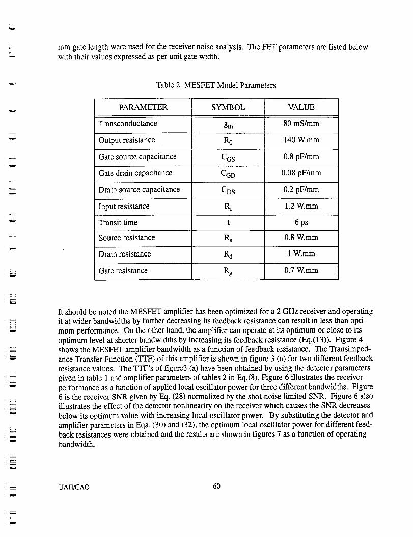
wmm gate length were used for the receiver noise analysis. The FET parameters are listed below
with their values expressed as per unit gate width.
Table 2. MESFET Model Parameters
w
W
- 7
w
w
w
PARAMETER SYMBOL VALUE
Transconductance gm 80 mS/mm
Output resistance Ro 140 W.mm
Gate source capacitance CGS 0.8 pF/mm
Gate drain capacitance CGD 0.08 pF/mm
Drain source capacitance Cos 0.2 pF/mm
Input resistance R i 1.2 W.mm
Transit time t 6 ps
Source resistance R s 0.8 W.mm
Drain resistance R_ 1 W.mm
Gate resistance Rg 0.7 W.mm
w
w
m
It should be noted the MESFET amplifier has been optimized for a 2 GHz receiver and operating
it at wider bandwidths by further decreasing its feedback resistance can result in less than opti-
mum performance. On the other hand, the amplifier can operate at its optimum or close to its
optimum level at shorter bandwidths by increasing its feedback resistance (Eq.(13)). Figure 4
shows the MESFET amplifier bandwidth as a function of feedback resistance. The Transimped-
ance Transfer Function (TTF) of this amplifier is shown in figure 3 (a) for two different feedback
resistance values. The TTF's of figure3 (a) have been obtained by using the detector parameters
given in table 1 and amplifier parameters of tables 2 in Eq.(8). Figure 6 illustrates the receiver
performance as a function of applied local oscillator power for three different bandwidths. Figure
6 is the receiver SNR given by Eq. (28) normalized by the shot-noise limited SNR. Figure 6 also
illustrates the effect of the detector nonlinearity on the receiver which causes the SNR decreases
below its optimum value with increasing local oscillator power. By substituting the detector and
amplifier parameters in Eqs. (30) and (32), the optimum local oscillator power for different feed-
back resistances were obtained and the results are shown in figures 7 as a function of operating
bandwidth.
m
UAH/CAO 60
w
L =w
W
.===
1 1 .... ................................... laeai Linear I]etector ""0.9o 6
,,, 0.5 GHzZ 0.8 l
O9 0.7 "0.60.5
_ 0.4
0.3Z 0.2
0.1
0 i _ I 1 ! +
0 0.5 1 1.5 2 2.5 3 3.5
Local Oscillator Power (mW)
w
w
w
i
lel
lie
Figure 6. Normalized SNR as a function of applied local oscillator power for a 2-micron
heterodyne receiver using MESFET transimpedance amplifier.
_-" 1.6
1.4
_1.2
0 1.0
-_ 0.8jo 0.6
E 0.4E 0.2"- 00 | | t I i IQ.
O 1.00E+08 1.00E+I 0
| i i • • • | i I i •
1.00E+09
Bandwidth (Hz)
Figure 7. Optimum local oscillator power versus bandwidth for MESFET transimpedance
amplifier
Substituting the numerical values of the optimum local oscillator power level for any given
bandwidth in Eq.(27), the contribution of each noise source were computed and the result is
shwon in figure 8. Figure 8 shows the level of noise powers due to each noise source and the total
receiver noise power as a function of bandwidth. It can be seen from figure 8 that the detector
shot noise is the dominating noise up to about 650 MHz. However, the amplifier input voltage
noise and the feedback thermal noise powers increase faster with bandwidth than the shot noise
with bandwith. The amplifier input voltage noise and feedback thermal noise increase
approximately as B 3 while the shot noise increase approximately as B 2. For the receiver being
UAH/CAO 61
__=
Ir=,_
investigated here, consisting of a 75 micron diameter, 2-micron detector and a 2 GHz MESFET
amplifier, the amplifier input voltage noise, also reffered to as the FET channel noise, starts todominate all other noises at about 2 GHz.
w
W
w
J
i
U
,<V
19
D_19
.m
OZ
1E-11
1E-12
1E-13
1E-14
1E-15
1E-16
1E+08 1E+09 1E+10
Bandwidth (Hz)
Figure 8.2-micron heterodyne receiver noise power with MESFET Transimpedance amplifier.
E_
The other two amplifiers considered for this work are a VF operational amplifier (CLC 425) and a
CF operational amplifier (CLC 449). Both amplifiers are among the fastest off-the-shelf
operational amplifiers manufactured by Comlinear with bandwidths greater than 1 GHz. Tables 3
and 4 provide selected parameters for these amplifiers that are necessary for design and analysis
of a heterodyne receiver. The TTF for these amplifiers are shown in figure 3 (b) and (c). The
TTF's have been obtained by using the detector parameters given in table 1 and amplifier
parameters given in tables 3 and 4 in Eq.(8) for two different feedback resistances. The receiver
bandwidths (Eq.(13)) for each of the amplifiers are shown in figure 4 as a function of feedback
resistance.
L
UAH/CAO 62
t ,
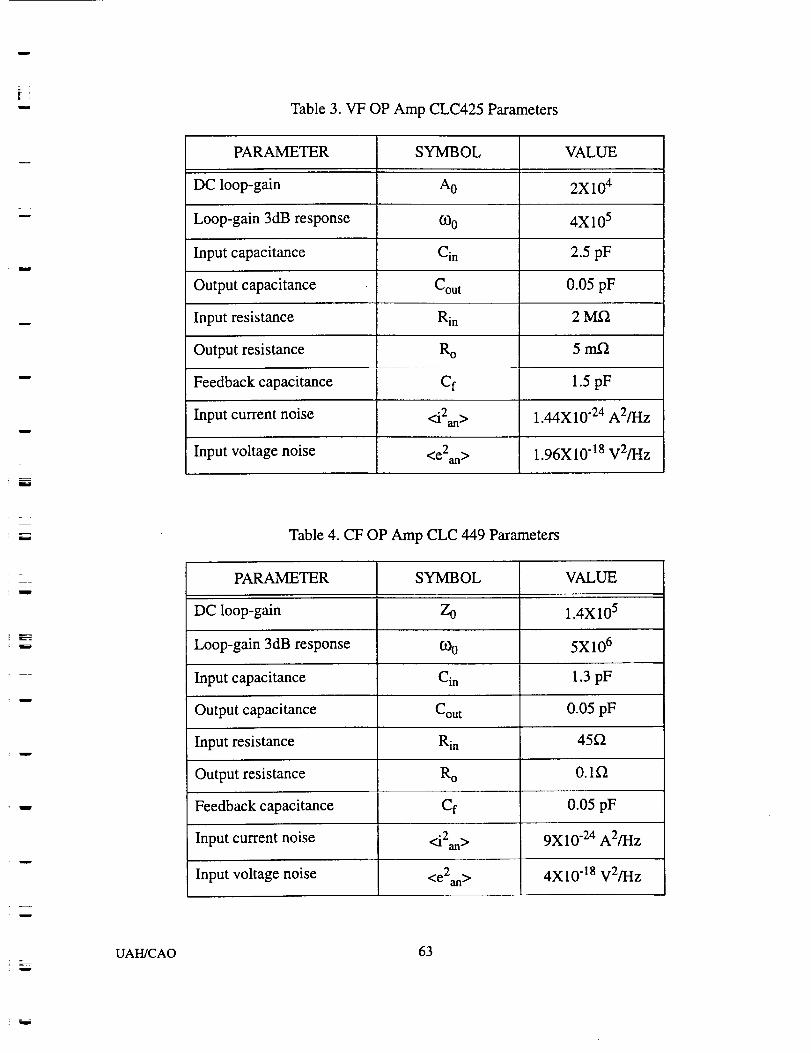
w
L_
w
UAH/CAO
Table 3. VF OP Amp CLC425 Parameters
PARAMETER SYMBOL VALUE
DC loop-gain AO 2X 10⁴
Loop-gain 3dB response COo 4X10⁵
Input capacitance Cin 2.5 pF
Output capacitance Cou t 0.05 pF
Input resistance Rin 2 Mf_
Output resistance R o 5 rn_
Feedback capacitance Cf 1.5 pF
Input current noise <i2an> 1.44X 10 "24 A2/Hz
Input voltage noise <e2an > 1.96X10 -18 V2/Hz
Table 4. CF OP Amp CLC 449 Parameters
PARAMETER SYMBOL VALUE
DC loop-gain
Loop-gain 3dB response
Input capacitance
Output capacitance
Input resistance
Output resistance
Feedback capacitance
Input current noise
Input voltage noise
Zo 1.4X10⁵
COo 5X 10⁶
Cin 1.3 pF
Cout
Rin
Ro
Cf
<i2an >
<e2an >
0.05 pF
45f_
0.1_
0.05 pF
9X 10-24 A2/Hz
4X10 -18 V2/Hz
63
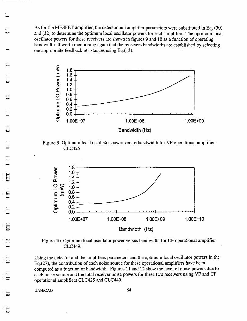
w
As for the MESFET amplifier, the detector and amplifier parameters were substituted in Eq. (30)
and (32) to determine the optimum local oscillator powers for each amplifier. The optimum local
oscillator powers for these receivers are shown in figures 9 and 10 as a function of operating
bandwidth. It worth mentioning again that the receivers bandwidths are established by selecting
the appropraite feedback resistances using Eq.(13).
w
F -
=W
r_
w
w
_" 1.8
E 1.6'- 1.4
1.2O
n 1.0O 0.8-_ 0.6E 0.4
E 0.2:_ 0.0o.O 1.00E+07
| | i | i i | | I . •
!
1.00E+08
• | | z _ |
1.00E+09
Bandwidth (Hz)
w
m,
mE
=
u
= =
w
w
=
Figure 9. Optimum local oscillator power versus bandwidth for VF operational amplifierCLC425
,-- 1.8
1.6o 1.4
m 1.2O'-"._ 1.oEEO.8= 0.6E 0.4
0.20 0.0 I I . . | . | iI I I | I I I | iA_ l . i . | | i .
1.00E+07 1.00E+08 1.00E+09 1.00E+10
Bandwidth (Hz)
Figure 10. Optimum local oscillator power versus bandwidth for CF operational amplifierCLC449.
Using the detector and the amplifiers parameters and the optimum local oscillator powers in the
Eq.(27), the contribution of each noise source for these operational amplifiers have been
computed as a function of bandwidth. Figures 11 and 12 show the level of noise powers due to
each noise source and the total receiver noise powers for these two receivers using VF and CF
operational amplifiers CLC425 and CLC449.
UAH/CAO 64
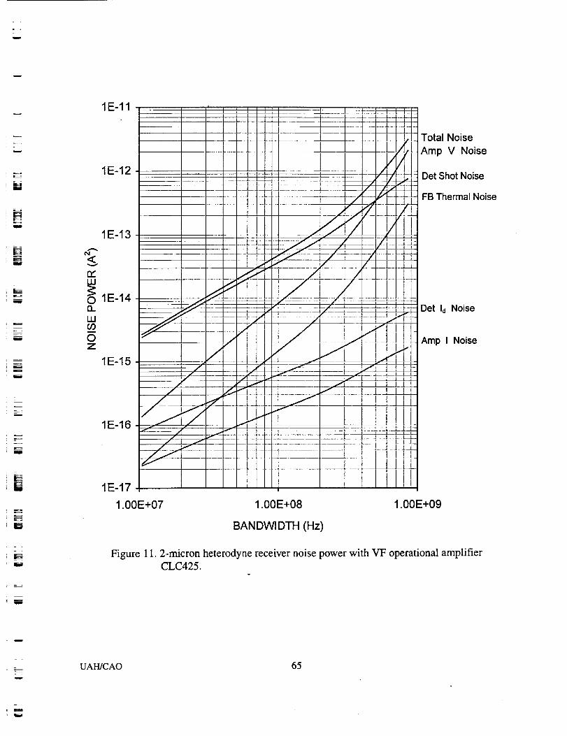
W
B
[]I
w
_=_
,EJ
W
<v
LU
13_
LUcou
OZ
1E-11
1E-12
1E-13
1E-14
1E-15
1E-16 -- __
1E-17 _
I
I II I
I I
!!I I
I1.00E+07 1.00E+08 1.00E+09
Total Noise
Amp V Noise
Det Shot Noise
FB Thermal Noise
Det Id Noise
Amp I Noise
BANDWIDTH (Hz)
Figure 11.2-micron heterodyne receiver noise power with VF operational amplifierCLC425.
w
w
UAH/CAO 65
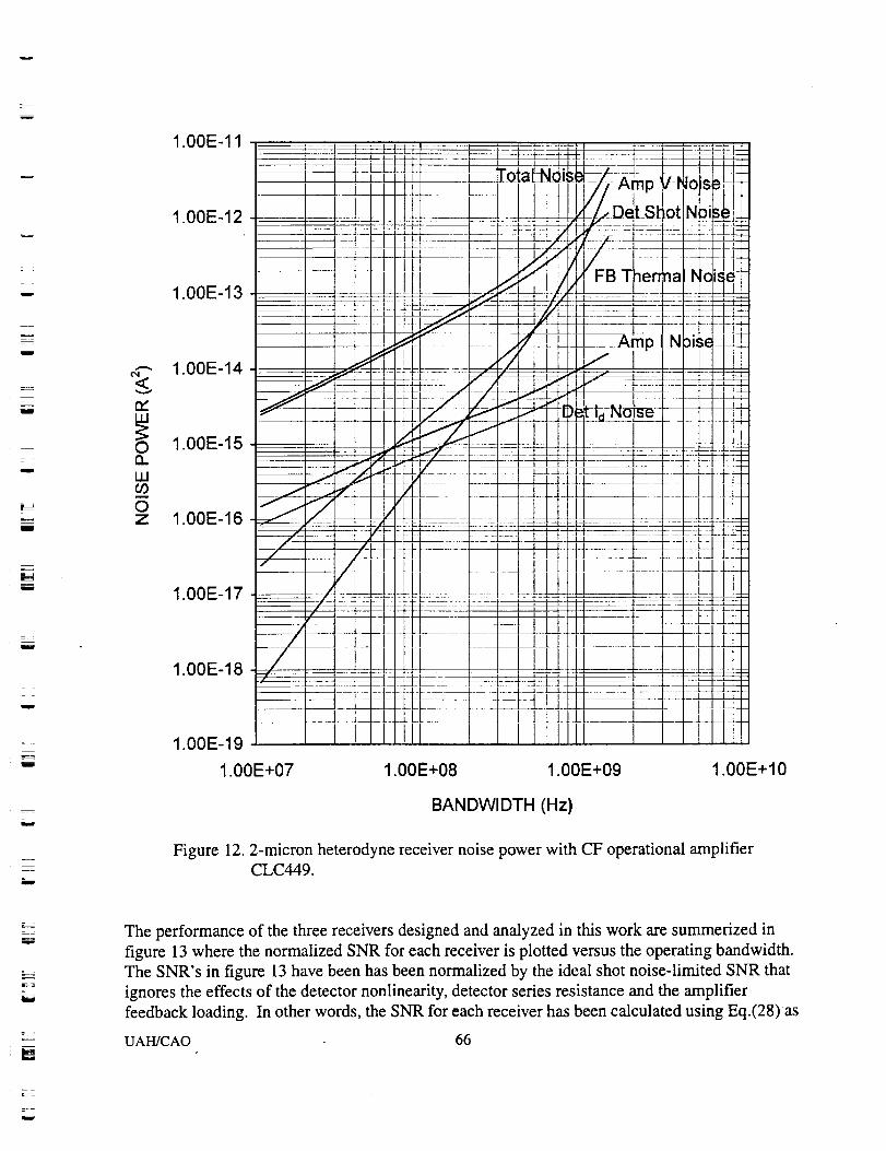
1.00E-11
w
w
E:m
w
Ew
E T
I
I
_m
I
W
¢N
re"LU
oQ.ILlO9oZ
1.00E-12
1.00E-13
1.00E-14
1.00E-15
1.00E-16
1.00E-17
1.00E-18
1.00E-19
1.00E+07 1.00E+08 1.00E+09 1.00E+ 10
BANDWIDTH (Hz)
Figure 12. 2-micron heterodyne receiver noise power with CF operational amplifierCLC449.
w
I
The performance of the three receivers designed and analyzed in this work are summerized in
figure 13 where the normalized SNR for each receiver is plotted versus the operating bandwidth.The SNR's in figure 13 have been has been normalized by the ideal shot noise-limited SNR that
ignores the effects of the detector nonlinearity, detector series resistance and the amplifier
feedback loading. In other words, the SNR for each receiver has been calculated using Eq.(28) as
UAH/CAO 66
w
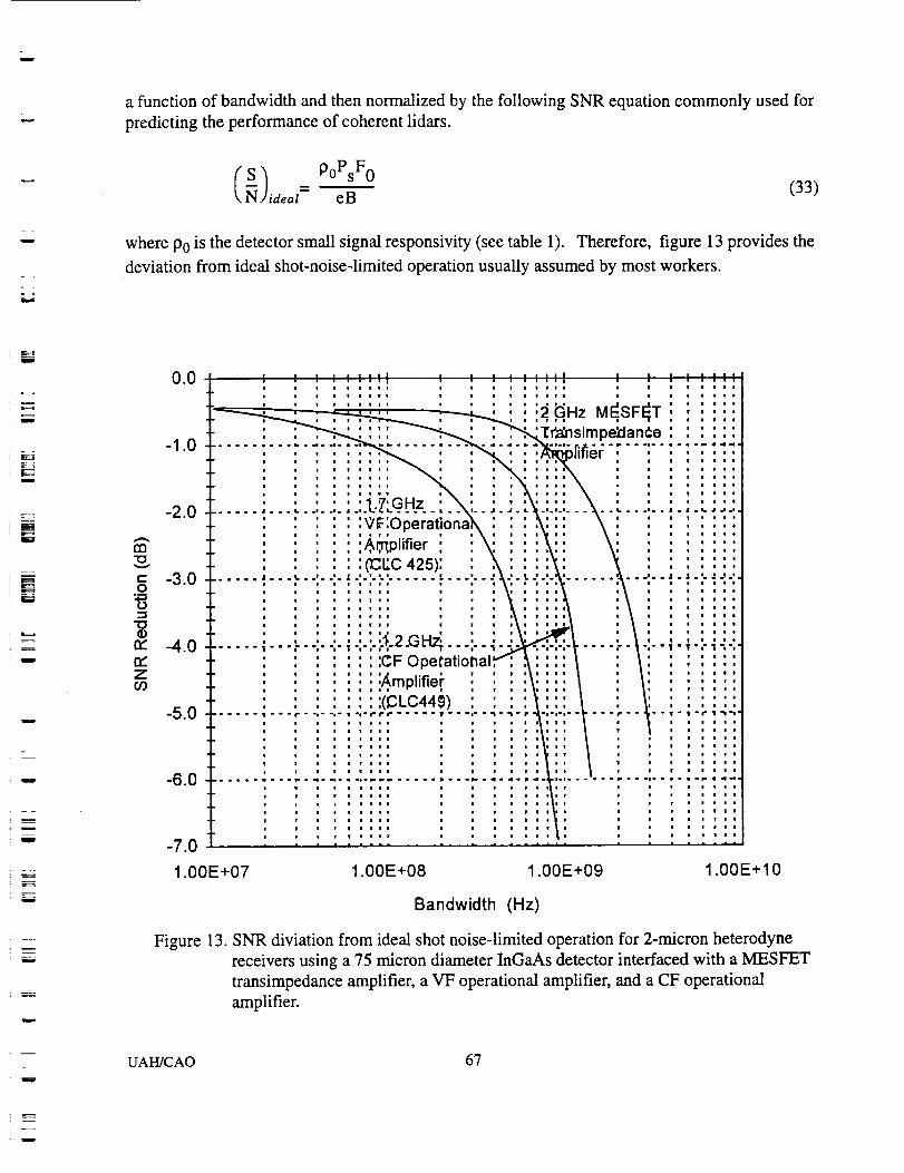
w
w
w
===
a function of bandwidth and then normalized by the following SNR equation commonly used for
predicting the performance of coherent lidars.
IS)ideal - P0PsF0 (33)eB
where P0 is the detector small signal responsivity (see table 1). Therefore, figure 13 provides the
deviation from ideal shot-noise-limited operation usually assumed by most workers.
i
- =
-2-_=
w
W
W
w
=
w
==
w
rn
V
e-.2
ZO9
0.0
-1.0
-2.0
-3.0 ........ '-- -'- -'-
-4.0 .............. ,-,-
-5.0 ......... , ...., .-,--,i _ e | a
''1 i I
:OF 0
!4mplifie',r :.
:(CLC449) :n | =
-6.0
-7.0
1.00E+07
i .... L LL.
1.00E+08
.... : ,::• = | i
|
1.00E+09 1.00E+IO
Bandwidth (Hz)
Figure 13. SNR diviation from ideal shot noise-limited operation for 2-micron heterodyne
receivers using a 75 micron diameter InGaAs detector interfaced with a MESFET
transimpedance amplifier, a VF operational amplifier, and a CF operational
amplifier.
W
UAI-I/CAO 67
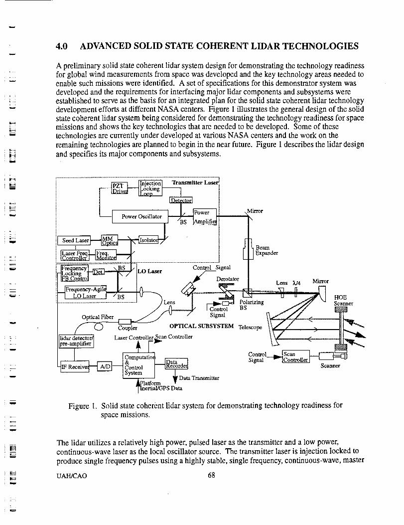
r ,
w
u
w
w
L
W
E_
w
m
!
w
L
f_
w
w
4.0 ADVANCED SOLID STATE COHERENT LIDAR TECHNOLOGIES
A preliminary solid state coherent lidar system design for demonstrating the technology readinessfor global wind measurements from space was developed and the key technology areas needed toenable such missions were identified. A set of specifications for this demonstrator system wasdeveloped and the requirements for interfacing major lidar components and subsystems wereestablished to serve as the basis for an integrated plan for the solid state coherent lidar technology
development efforts at different NASA centers. Figure 1 illustrates the general design of the solidstate coherent lidar system being considered for demonstrating the technology readiness for spacemissions and shows the key technologies that are needed to be developed. Some of these
technologies are currently under developed at various NASA centers and the work on the
remaining technologies are planned to begin in the near future. Figure 1 describes the lidar design
and specifies its major components and subsystems.
Mirror
Seed Laser
Beal_
Expander
LO Laser Control Signal
DerotatorLens ),/4 Mirror
LO Laser
Optical Fiber
lidar detector_
pre-amplifierJ
Lens PolarizingControl BS
Signal
Coupler OPTICAL SUBSYSTEM Telescope
Laser Controller Scan Controller
Computatio_
ControlSystem
Data Transmitterafform
ertial/OPS Data
Control
Signal
HOEScanner
Scanner
Figure 1. Solid state coherent lidar system for demonstrating technology readiness forspace missions.
The lidar utilizes a relatively high power, pulsed laser as the transmitter and a low power,continuous-wave laser as the local oscillator source. The transmitter laser is injection locked to
produce single frequency pulses using a highly stable, single frequency, continuous-wave, master
UAH/CAO 68
w
= :
w
w
u
_-w_qw
w
E
MW
W
oscillator laser. Part of the master oscillator laser is also used for controlling the local oscillator
laser frequency that varies with the scanner position. Variable local oscillator frequency
compensates for gross spacecraft-induced Doppler shift. A simplified schematic of a CLR is
shown in Figure 1. The pulsed laser output beam is expanded by an off-axis telescope to be
transmitted to the atmosphere. The quarter-wave plate placed along the propagation path changes
the polarization of the transmitted beam from vertical to circular. The retum beam from the
atmosphere is received by the same telescope and directed through the quarter-wave plate and a
polarizing beamsplitter toward the detector. The derotator and lag angle compensator (LAC)13,14
placed along the return signal path to correct for the boresight and wavefront errors caused by the
scanner and spacecraft motions. At the detector the return radiation is mixed with the local
oscillator beam for heterodyne detection. The detector in tum generates an electrical signal at the
difference frequency between the signal and local oscillator frequencies. The output of the
detector is then bandpass filtered and amplified to be digitized and processed for Doppler
frequency shift due to the atmospheric winds.
A transmitter laser system is currently being developed at NASA Langley Research Center and a
frequency-agile local oscillator laser is being developed at NASA Jet Propulsion Laboratory.
UAH personnel has been working with the NASMMSFC engineer and scientists towards the
development of the other lidar subsystems including the lidar heterodyne receiver and the
transmitter/receiver optical assembly. The work on the heterodyne receiver is described in
chapters 2 and 3, and the work on the optical subsystem is described in this chapter and chapters 5and 6.
The followings summarize the general lidar specifications and the requirements for the transmitter
and local oscillator laser subsystems.
LidarTelescope clear aperture diameter
Scanning angle
Scanning frequency
Total optical throughputDetection bandwidth
Detector heterodyne quantum efficiency
Heterodyne mixing efficiency
IF signal frequency resolution
Doppler signal bandwidth
Transmitter Laser
Pulse energyPulse width
Pulse repetition rate
Wavelength
Output polarization
MO short term frequency jitter
UAH/CAO 69
25 cm
30 °
10 RPM
>90%
1 GHz
>0.6
>0.3
IOOKHz
1O0 MHz
500 mJ
500 nsec
10 Hz
2065 nm
98% Linear
<10 KHz/msec
w
w
z
w
r_
w
-£
m
w
w
m
r_
_.=_
!
W
EE
_=
w
MO long term frequency stabilityLaser linewidth
Pulse to pulse frequency stability
MO power stability
Pulse energy stability
MO laser power available to LO laser
Beam quality
Electrical to optical efficiency
< 100 MHz/hr
<2.5 MHz
<10 MHz
<5% peak-to-peak, 1 sec5%
2 mW
<i. 1XD.L.
5%
_-agile local oscillator Laser
Output power
Power stability
Output polarization
Short term frequency jitter
Continuous frequency tuning bandwidth
Average tuning speed
Maximum tuning speed
Beam quality
25 mW
<5% peak-to-peak, 1 sec
98%Linear
<100 KHz/msec
7.9 GHz
1.3 GHz/sec
8.2 GHz/sec
<I.IXD.L.
The NASA's plan is to developed a breadboard lidar based on these requirements to evaluate the
advanced lidar technologies under development and to demonstrate the technology readiness of
solid state coherent lidar for low-cost small satellite and shuttle missions.
The transmitter/receiver optical subsystem includes the transmitter/receiver telescope, the return
signal de-rotator, the lag angle compensator, and the scanner. The design and analysis of an
advanced monolithic signal beam de-rotator is described in the next chapter, the telescope design
along with a complete tolerance and performance analyses is explained in chapter 5, and the effort
on the low-mass scanner is explained in this chapter.
4.1 HOLOGRAPHIC AND DIFFRACTIVE OPTICAL ELEMENT SCANNERS
A study was initiated in this period to determine the feasibility of using Diffractive and
Holographic Optical Elements (DOE and HOE) for scanning the lidar transmitter beam (see
figure 1). The diffractive and holographic optical elements have the potential of substantially
reducing the mass of the lidar systems and allowing for a much easier spacecraft accommodation
design. The diffractive and holographic optical elements change the direction of a laser beam by
diffraction, as opposed to the conventional scanning techniques that are based on refraction and
reflection. The diffractive and holographic optical elements can potentially reduce the mass of the
lidar scanner to less than one fourth of a wedge scanner with the same clear aperture diameter.
Wedge scanners have frequently been used in the past for airborne lidar measurements and is now
being considered for spaceborne measurements.
As part of this effort, an advanced holographic photopolymer material was experimentally
evaluated at 2 microns wavelength. This holographic material, developed by Dupont, is
UAH/CAO 70
w []
w
w
w
u
w
insensitive to environment and more rugged compared to more conventional dichromated gelatin
(DCG) holographic material that is sensitive to moisture and need to sealed. To experimentally
evaluate the holographic polymer material, a 10-micron thick film was recorded and its properties
were measured. The recorded pattern was designed for deflecting a 2-micron beam by 30
degrees. Using the U.S. Army Missile Command laboratory facilities in Huntsville and an argon-
ion laser, several holographic films were exposed by two 2 mW beams at normal and 100 off
normal over different time periods. The films were then measured at 633,859, 1300 and 2067 nm
wavelengths before and after baking the films at different temperature and over different time
spans. The experimental data showed that both the refractive index depth of modulation and
deflection efficiencies decrease with increasing wavelength. The change in refractive index with
20 seconds of exposure was measured to be about 0.014 and 0.007 at 633 nm and 2067 nm before
baking, and 0.036 and 0.010 after baking the f'dm at 120°C for two hours. The correspondingdeflection efficiencies were measured to be 0.94 at 633 nm and 0.04 at 2067 nm before baking,
and 0.22 and 0.09 after baking the fflm. The results were consistent with the analytical
predications, which shows that the deflection efficiency can be considerably improved by using a
much thicker t-tim of about 100 microns. Unfortunately, such thick holographic film was not
available at the time of this work. The thickest film Dupont could provide was 50 microns which
was acquired by MSFC to be processed and measured at a later time.
UAH also specified an experimental HOE scanner, using dichromated gelatin (DCG) holographic
material, to be fabricated and measured for 2-micron operation. This scanner was fabricated by
the Teledyne Brown Engineering (TBE) and delivered to MSFC. This scanner consists two 15 cm
substrates with the holographic material sealed between them. The actual useful area has a 10 cm
diameter. This scanner will be measured at 2 microns wavelength by the UAH personnel in the
DCF at MSFC.
UAH recommends to continue this work by investigating, both analytically and experimentally,
other HOE and DOE techniques such as diamond turning, photolithography and laser writing.
The analytical work is to include the development of a model using the exact electromagnetic
vector field theory to predict the performance of different technique and to optimize their designs.
These designs can then be used to fabricate a number of experimental scanning elements. UAH
personnel can then use the DCF and other MSFC optical laboratories to fully evaluate the
properties of the experimental elements for use in 2-micron coherent lidars.
_ L_
L
w
L
UAH/CAO 71
F_
w
!
5.0 SIGNAL BEAM DE-ROTATOR
In principle, a coherent Doppler lidar uses naturally occurring atmospheric aerosols to scatter
transmitted radiation from a laser back to a receiver where the Doppler frequency shift is used to
measure the air motion radial velocity. The Doppler shift is extracted by utilizing heterodyne
detection for which the frequency of the detectable signal is equal to the difference frequencies
between the return radiation and a reference local oscillator beam. Since the Doppler lidars
provide the wind velocity component along the line-of-sight of the transmitted beam, the wind
vector velocity is determined by pointing the transmitted beam to at least three different
directions 16-19. The most conventional method of directing the laser beam to different directions
and effectively measuring the atmospheric wind fields by a Doppler lidar, either from a ground, or
airborne, or a spaceborne platform, is the conically-scanning technique which generates a circular
pattern in the target plane 20-22. However, the lidar performance is greatly affected by the motion
of the scanner during the transmitted pulse round trip time. As the laser energy reflects off the
atmospheric aerosols and travels back to the lidar telescope, the scanner continues to move
causing signal beam to follow a different path through the telescope than that of the transmitted
beam. Therefore as the scanner continues to rotate and the transmitted beam sweeps a conical
pattern in the atmosphere, the received signal beam orbits about the optical axis that extends to the
lidar photodetector and coincides with the local oscillator beam. In a Doppler lidar system,
utilizing optical heterodyne detection, the relative alignment of the received signal with respect to
the local oscillator beam is particularly critical. This is due to the fact that the mean power of the
electronic signal generated by the photodetector decreases exponentially with the angle between
e-a_the signal and local oscillator beams y, that is is o_ . For ground-based and airborne
applications, this effect limits the scanning frequency and consequently the lidar update rate. For
spaceborne measurements of the earth's wind fields, the scanner motion must be compensated for
any reasonable scanning frequency due to very long propagation path of several hundreds of
kilometers. This invention provides a simple and robust mechanism for compensating the scanner
motion and allowing for optimum laser radar operation.
Previously, a rotating periscope has been proposed for a spaceborne lidar system to maintain the
received beam along a fixed axis to the laser radar detector as the scanner rotates about its
axis 13'14. Another approach is the stop-and-steer scanning technique that allows sufficient time
for the signal beam to be received before the scanner begins to move to its next position 15. A
novel but simple signal de-rotator scheme has been developed under this work that provides a low
mass, compact and robust alternative to rotating periscopes and stop-and-steer techniques. In
addition to spaceborne applications, this scheme is also ideal for use in airborne systems for
which the compactness and ruggedness are critical design issues.
5.1 PRINCIPLE OF OPERATION
The signal beam de-rotator that has been devised utilizes a monolithic optical element for
maintaining the received signal beam with respect to the local oscillator beam along a fixed axis to
UAH/CAO 72
w
w
w
w
w
z
W
i==a
I
mz
Z Z
m
w
mw
w
the lidar photodetector. The de-rotator performs two functions: changing the signal beam
direction to be continuously parallel to the optical axis, and translating the signal beam to the
optical axis that coincides with the local oscillator beam and extends to the photodetector. By
synchronizing the rotation of the de-rotator about the optical axis with that of the scanner, the
signal beam is then maintained along the optical axis and aligned with respect to the local
oscillator beam
The de-rotator optical substrate has two plane surfaces that are inclined with respect to each other
at a relatively small wedge angle. The de-rotator substrate is selected from the optical materials
with relatively high optical transmission and high index of refraction at the operating wavelength
to minimize the absorption losses of signal. For operation in near-infrared region, the optical
substrate material may be Silica, Zinc Selenide, Zinc Sulfide, or Germanium. The de-rotator
optical element is placed on the return signal beam path at 45 degrees angle with respect to the
optical axis. The plane of the optical element, defined by the vectors normal to its surfaces, is set
to be parallel to plane of the incident signal beam and the optical axis as shown in figures 1 and 3.
Since the signal beam incident on the de-rotator substrate rotates about the optical axis with the
scanner, as illustrated in figure 1, the de-rotator substrate must also rotate to sustain its relative
orientation with respect to the signal beam. Since the de-rotator substrate has a different index of
refraction than the free space, the signal beam translates in the plane of the optical element. This
translation distance is directly related to the substrate thickness and refractive index. The de-
rotator substrate also changes the signal beam direction by an angle that is directly related to its
wedge angle and refractive index.
Figure 1 illustrates the operation of the de-rotator in a lidar system. The lidar transmitter/receiver
telescope is an off-axis parabolic telescope and its scanner is an optical wedge• It should be noted
that the optical wedge scanner may be replaced by a holographic or a diffractive optical element
without loss of generality for the analysis and formulations described below. The purpose of the
telescope is to expand the transmitter beam and collect the return signal scattered off the target.
The off-axis telescope has the advantage of high isolation between the transmitter and return
radiations• In figure 1, the transmitted beam is reflected off a polarizing beamsplitter before being
expanded by the telescope. The optical wedge deflect the beam in a plane defined by the normal
vectors to its surfaces. As the optical wedge rotates along its axis, the transmitted beam scans a
circular pattern at the target plane. The deflection angle for an optical wedge is given by:
• 2sin (0) = sin (cx) _n 2- sm ((x) - sin (o0 cos (o0 (1)
where c_ is the scanner wedge angle and n is its index of refraction. For a given optical material
with a known index of refraction, the wedge angle necessary for providing a desired scanning
angle can be determined by:
,(1H+ l+n22H)o_ = 2tan sin (0)(2)
where H = ,_n 2- sin2(0)
UAH/CAO 73
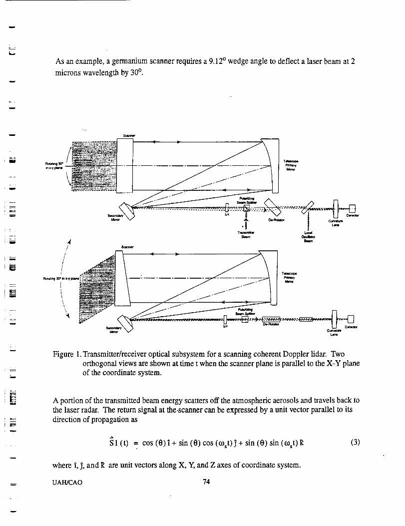
As an example, a germanium scanner requires a 9.12 ° wedge angle to deflect a laser beam at 2
microns wavelength by 30°.
=
r_
w
2
r _
w
m
w
w
Figure 1. Transmitter/receiver optical subsystem for a scanning coherent Doppler lidar. Two
orthogonal views are shown at time t when the scanner plane is parallel to the X-Y planeof the coordinate system.
m
hE
A portion of the transmitted beam energy scatters off the atmospheric aerosols and travels back to
the laser radar. The return signal at the,scanner can be expressed by a unit vector parallel to its
direction of propagation as
S1 (t) = cos (O)i+ sin (e) cos (o_t)j + sin (O) sin (O_st) It (3)
where i, j, and It are unit vectors along X, Y, and Z axes of coordinate system.
UAH/CAO 74
r_
w
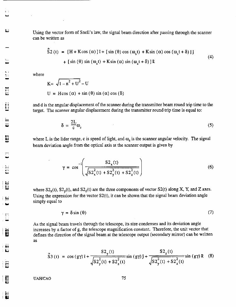
r =
Using the vector form of Snell's law, the signal beam direction after passing through the scannercan be written as
=-- 2
U
ziz_
w
w
m
m
W
W
-- L
w
-%
S2(t) = [H + Kcos (o0 ] i + [ sin (0) cos (COst) + Ksin (o0 cos (COst + 5) ]j
+ [sin (0) sin (COst) + Ksin (or) sin (COst+ 8) ] _:
(4)
where
2K= _/1-n +U2-U
U = Hcos (cz) + sin (0) sin (o0 cos (8)
and d is the angular displacement of the scanner during the transmitter beam round trip time to the
target. The scanner angular displacement during the transmitter round trip time is equal to:
2L
8 = TCO= (5)
where L is the lidar range, c is speed of light, and COsis the scanner angular velocity. The signal
beam deviation angle from the optical axis at the scanner output is given by
_1I S2 x (t)y = cos A/S2_ (t) + $2_ (t) + $22z (t)
(6)
L-
w
J
m_
L
W
where S2x(t ), S2y(t), and S2z(t) are the three components of vector S2(t) along X, ¥, and Z axes.
Using the expression for the vector S2(t), it can be shown that the signal beam deviation angle
simply equal to
y = I sin (0) (7)
As the signal beam travels through the telescope, its size condenses and its deviation angle
increases by a factor of g, the telescope magnification constant. Therefore, the unit vector that
defines the direction of the signal beam at the telescope output (secondary mirror) can be written
as
S2y (t) $2 z (t)$3 (t) = cos (gy)i+ sin (gy)j+ sin (gy) It (8)
A/S21 (t)+ $22z (t) _/$22y (t) + S22z(t)
UAH/CAO 75
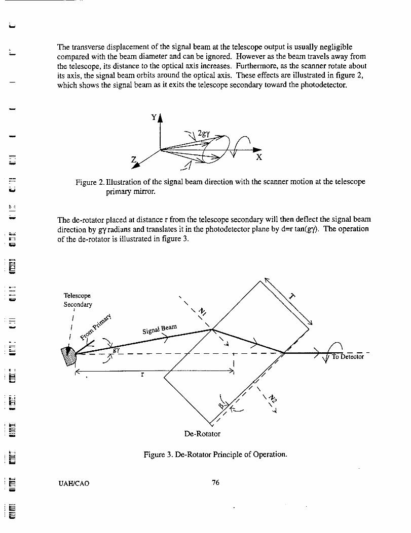
w
w
I
F_!
w
The transverse displacement of the signal beam at the telescope output is usually negligible
compared with the beam diameter and can be ignored. However as the beam travels away from
the telescope, its distance to the optical axis increases. Furthermore, as the scanner rotate about
its axis, the signal beam orbits around the optical axis. These effects are illustrated in figure 2,
which shows the signal beam as it exits the telescope secondary toward the photodetector.
Figure 2. Illustration of the signal beam direction with the scanner motion at the telescope
primary mirror.
The de-rotator placed at distance r from the telescope secondary will then deflect the signal beam
direction by g7 radians and translates it in the photodetector plane by d=r tan(gT). The operation
of the de-rotator is illustrated in figure 3.
J
!
w
E
w
W
r 7iwE
i
Telescope , __,_,
Secondary \ / _, \ _ / \\
I "/
De-Rotator
/ x_/To Detector
Figure 3. De-Rotator Principle of Operation.
UAH/CAO 76
=
w
J
m
E._2
w
Ili
L
w
w
w
The signal beam experiences a change of direction by both input and output surfaces of the de-
rotator. The direction of the signal beam as it propagates through the de-rotator substrate, can be
expressed as following.
(Jnd2 2 )NX I,S4(t) - S3(t) + -l+(S3(t).Nl(t)) -S3(t).Nl(t) • (9)n d nd
Where n d is the index of refraction of the de-rotator substrate, and N 1 is the unit vector normal to
the de-rotator input surface given by
dr2I^ S2y(t) .__ S2z(t) ]2 _ - - 2 2 + $22z l_Nl(t) = -_- x-4/S2y(t ) +S2z(t) ,,/S2y(t) (t)
(10)
The signal beam, deflected by the input surface of the de-rotator, crosses the optical axis exactly at
the de-rotator output surface. Therefore by using the above expression for the signal beam
direction inside the de-rotator and performing some mathematical manipulations, a formulation
for specifying the thickness of the de-rotator substrate was derived.
r tan (gT) _2(n_ - sin2(4 + gT))T = (11)
Jn2d - sin2(4 + gY) - sin(4 + gY) (1 - tan (gT))
where r is the distance from the telescope secondary to the center of the de-rotator.
The signal beam unit vector exiting the de-rotator output surface can be written in a similarfashion as
S5(t) = nd. S4(t) + l--rid2+ (nd. S4(t ) .N2(t)) - (na. S4(t).N2(t)) .N2(t)
(12)
where N2 is the unit vector normal to the de-rotator output surface given by
N2(t) cos(4 -'L sinai. +. [3_))
= + _)'-_$22y (t) + S22z(t)
(S2y (t) j + $2 z (t) 1_) (13)
where 13is the wedge angle of the de-rotator substrate. By setting S 5 (t) equal to i, an expression
UAH/CAO 77
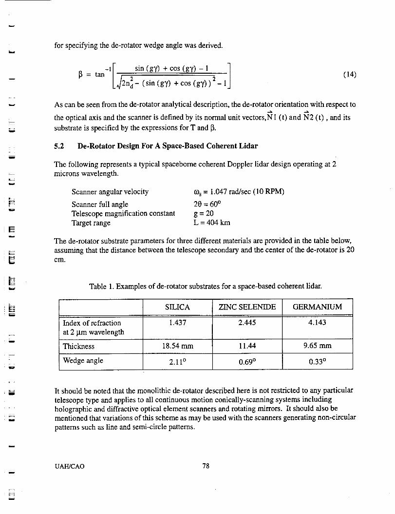
s
=
u
k
w
for specifying the de-rotator wedge angle was derived.
[3= tan
n_ - (sin (gT) + cos (gy)) 1
(14)
As can be seen from the de-rotator analytical description, the de-rotator orientation with respect to
the optical axis and the scanner is defined by its normal unit vectors,N1 (t) and N2 (t), and its
substrate is specified by the expressions for T and [3.
5.2 De-Rotator Design For A Space-Based Coherent Lidar
The following represents a typical spacebome coherent Doppler lidar design operating at 2
microns wavelength.
Scanner angular velocity
Scanner full angle
Telescope magnification constant
Target range
cos = 1.047 rad/sec (10 RPM)
20 = 60 °
g=20L = 404 km
The de-rotator substrate parameters for three different materials are provided in the table below,
assuming that the distance between the telescope secondary and the center of the de-rotator is 20
cm.
t_
[]Table 1. Examples of de-rotator substrates for a space-based coherent lidar.
= =
w
SILICA ZINC SELENIDE GERMANIUM
Index of refraction 1.437 2.445 4.143
at 2 ktm wavelength
Thickness 18.54 mm 11.44 9.65 mm
Wedge angle 2.11 ° 0.69 ° 0.33 °
It should be noted that the monolithic de-rotator described here is not restricted to any particular
telescope type and applies to all continuous motion conically-scanning systems including
holographic and diffractive optical element scanners and rotating mirrors. It should also be
mentioned that variations of this scheme as may be used with the scanners generating non-circular
patterns such as line and semi-circle pattems.
w
UAH/CAO 78
= ,
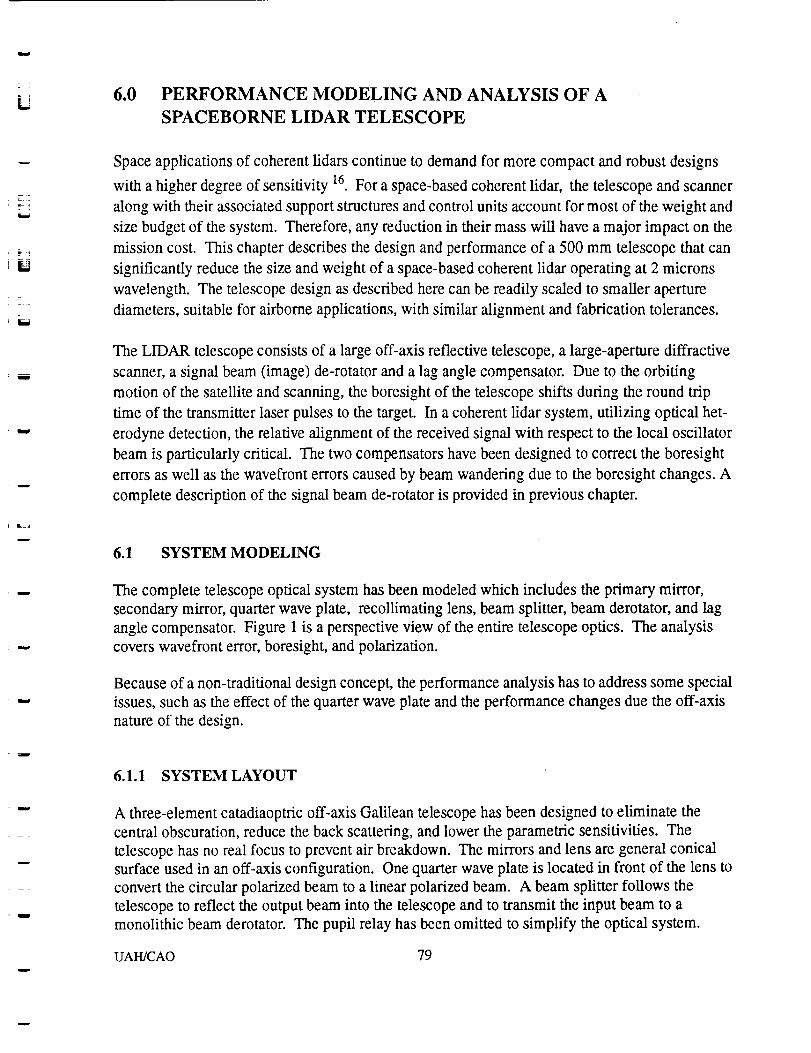
6.0 PERFORMANCE MODELING AND ANALYSIS OF A
SPACEBORNE LIDAR TELESCOPE
w
w
m
u
n
Space applications of coherent lidars continue to demand for more compact and robust designs
with a higher degree of sensitivity 16. For a space-based coherent lidar, the telescope and scanner
along with their associated support structures and control units account for most of the weight and
size budget of the system. Therefore, any reduction in their mass will have a major impact on the
mission cost. This chapter describes the design and performance of a 500 mm telescope that can
significantly reduce the size and weight of a space-based coherent lidar operating at 2 microns
wavelength. The telescope design as described here can be readily scaled to smaller aperture
diameters, suitable for airborne applications, with similar alignment and fabrication tolerances.
The LIDAR telescope consists of a large off-axis reflective telescope, a large-aperture diffractive
scanner, a signal beam (image) de-rotator and a lag angle compensator. Due to the orbiting
motion of the satellite and scanning, the boresight of the telescope shifts during the round trip
time of the transmitter laser pulses to the target. In a coherent lidar system, utilizing optical het-
erodyne detection, the relative alignment of the received signal with respect to the local oscillator
beam is particularly critical. The two compensators have been designed to correct the boresight
errors as well as the wavefront errors caused by beam wandering due to the boresight changes. A
complete description of the signal beam de-rotator is provided in previous chapter.
6.1 SYSTEM MODELING
The complete telescope optical system has been modeled which includes the primary mirror,
secondary mirror, quarter wave plate, recollimating lens, beam splitter, beam derotator, and lag
angle compensator. Figure 1 is a perspective view of the entire telescope optics. The analysis
covers wavefront error, boresight, and polarization.
Because of a non-traditional design concept, the performance analysis has to address some special
issues, such as the effect of the quarter wave plate and the performance changes due the off-axis
nature of the design.
6.1.1 SYSTEM LAYOUT
A three-element catadiaoptric off-axis Galilean telescope has been designed to eliminate the
central obscuration, reduce the back scattering, and lower the parametric sensitivities. The
telescope has no real focus to prevent air breakdown. The mirrors and lens are general conical
surface used in an off-axis configuration. One quarter wave plate is located in front of the lens to
convert the circular polarized beam to a linear polarized beam. A beam splitter follows the
telescope to reflect the output beam into the telescope and to transmit the input beam to a
monolithic beam derotator. The pupil relay has been omitted to simplify the optical system.
UAH/CAO 79
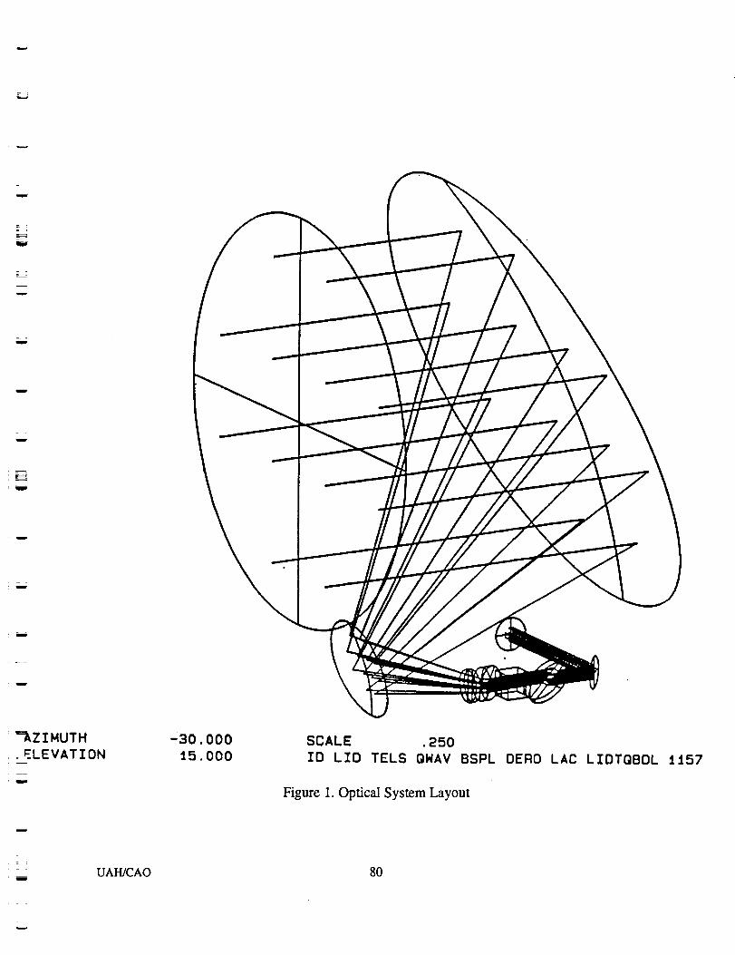
w
i
w
m
w
w
w
w
w
'_kZIMUTH
ELEVATION
w
zu
L
i
UAH/CAO
"30.000
15.000SCALE .250
IO LID TELS QHAV BSPL OERO LAC LIOTQBOL t157
Figure 1. Optical System Layout
80
w
= The beam derotator removes both the angular and linear displacements caused by the scanner and
telescope. A single electro-mechanically controlled folding mirror has been used to perform the
lag angle compensation.
The primary mirror, secondary mirror, and recollimating lens share the total optical power to
lower the parametric sensitivity. The conical constants of the secondary mirror and two lens
surfaces are also optimized to achieve the overall optical performance.
w
uw
m
B
m
w
w
m
W
W
m
m
m_
6.1.2 THE EFFECT OF THE QUARTER WAVE PLATE
The quarter wave plate is located in the convergent ray path. Any parallel plate in the non-
collimated ray path will introduce aberrations. In the design, a fused silica plate has been added
to model this effect. The telescope optics has to be re-optimized to obtain an acceptable
performance. The surface shape of the mirrors as well as the lens changes slightly after
introducing the quarter wave plate. The locations of the mirrors and the lens stay same.
The sensitivity analysis shows that the performance is not sensitive to the location of the quarter
wave plate. The performance is sensitive to the thickness and wedge errors of the plate. The tilt of
the element has little effect on the performance.
6.2 PERFORMANCE
The system specifications are as follows:
Magnification 25 X
Entrance aperture 500 mm
Exit pupil 20 mm
Overall axial length 400 mmOff-axis value 375 mm
Wavelength 2.067 micron
Field of view 0.0802 degree
(afocal)
(diameter)
(diameter)
(conical scan angle)
The performance analysis as well as the sensitivity analysis have not included the scanner effects.
The conical scan field of view has been considered in the modeling and analysis.
6.2.1 WAVEFRONT PERFORMANCE
Wavefront error has been used to quantitatively describe the beam quality of the telescope. The
RMS wavefront error of less 1/10 wave is required for the coherent operation. The design has
been optimized to achieve much lower wavefront errors. This leaves enough margin for the
fabrication and integration tolerances.
UAH/CAO 81
w
6.2.1.1 OFF-AXIS EFFECT
Because of the off-axis operation of the telescope, the field characteristics of the performance are
not symmetric. The performance can not be simply checked only on-axis and at fullfield as in the
traditional rotation symmetrical system. However, the field character is piano symmetrical. We
have checked the performances at the (1) center of the field, (2) top most field, (3) lower most
field, and (4) right most field. Left most field is mirror symmetrical to the right most field.
6.2.1.2 WAVEFRONT FOR THE EMITTING BEAM AND RETURNING BEAM
AT DIFFERENT FIELD ANGLES
Figures 2 to 5 are the plots of the wavefront maps at different field angles. The RMS wavefronterrors are:
w
W
w
L_
w
0.0034 wave
0.0040 wave
0.0085 wave
0.0087 wave
(At the top most field shown in Figure 2)
(At the low most field shown in Figure 3)
(At the right most field shown in Figure 4)
(At the center of the field shown in Figure 5, output path)
The peak-to-valley errors are also well below requirements.
6.2.2 BORESIGHT
The boresight is the other most important performance parameter of the optical system for a
coherent operation. An error of 1 micro-radians is required in the object space.
6.2.2.1 DISTORTION PROBLEM
m
w
[]
--_::__'-
w
The distortions of the off-axis optics are not axial symmetrical anymore. The beam with a conical
scan motion will have slight ray angle changes at different scanning clock angles caused by the
non-symmetrical distortions. It will be a nightmare to correct this kind of error. Therefore,
distortion check has to be performed to ensure the ray angle uncertainty is within the boresight
requirement.
6.2.2.2 BORESIGHT AT DIFFERENT BEAM ANGLE
The boresight error at different scanning positions are listed:
0.365 micro-radians
0.365 micro-radians
0.271 micro-radians
(At top most of the field)
(At low most of the field)
(At right most of the field)
The boresight error introduced by other parts, such as the beam derotator and lag angle
compensator is controlled by the tolerances of these parts.
UAH/CAO 82
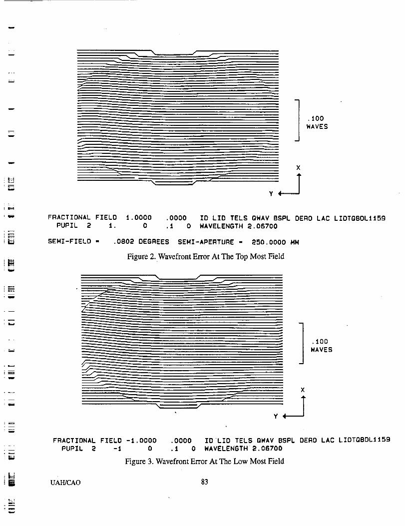
m
w
w
\ / f
% 1!' i
X
.t00
WAVES
i
w
FRACTIONAL FIELD 1.0000
PUPIL 2 I. O
• 0000 IO LID TELS OWAV BSPL DERO LAC LIDTQBDLtt59
.1 0 WAVELENGTH 2.06700
SEMI-FIELD = .0802 DEGREES SEMI-APERTURE = 250.0000 MM
Figure 2. WaveffontE_or AtTheTopMostField
\ /
.- XJ
J Y/
.100WAVES
FRACTIONAL FIELD -1.0ODD
PUPIL 2 -1 0
.OOO0 IO LID TELS QWAV BSPL DERO LAC LIDTOBOLlt59
.t O WAVELENGTH 2.06700
Figure 3. Wavefront Error At The Low Most Field
UAH/CAO 83
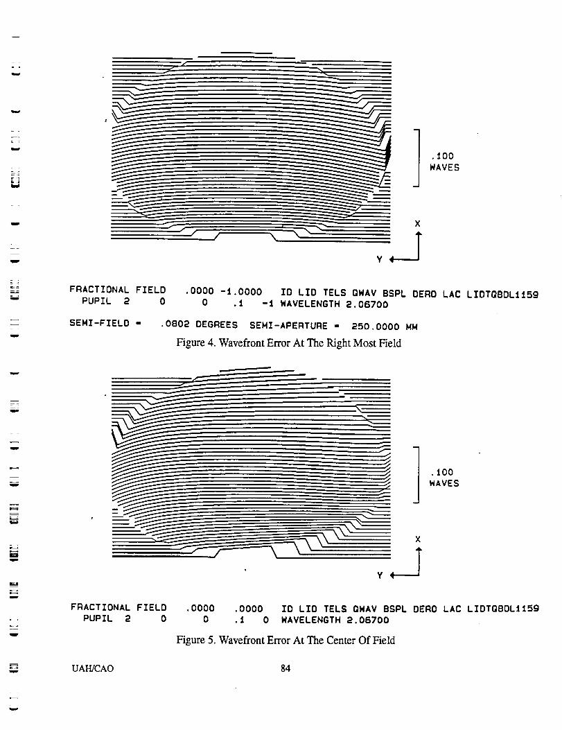
J_
-'hf
r
r _, ,,,
1.100HAVES
/ / \
FRACTIONAL FIELD
PUPIL 2 0•O00O -t.0000 IO LID TELS OWAV BSPL DERO LAC LIDTQBDLII59
0 .t -t WAVELENGTH 2.06700
SEMI-FIELD = .0802 DEGREES SEMI-APERTURE - 250.0000 MM
Figure 4. Waveffont E_or At The Right Most Held
Ez=_
= =
m
W
FRACTIONAL FIELDPUPIL 2 0
UAH/CAO
P
• tO0WAVES
.00000
.OOO0 IO LID TELS OHAV BSPL DERO LAC LIDTQBOLtC59.t 0 WAVELENGTH 2.06700
Figure 5. Wavefront Error At The Center Of Field
84
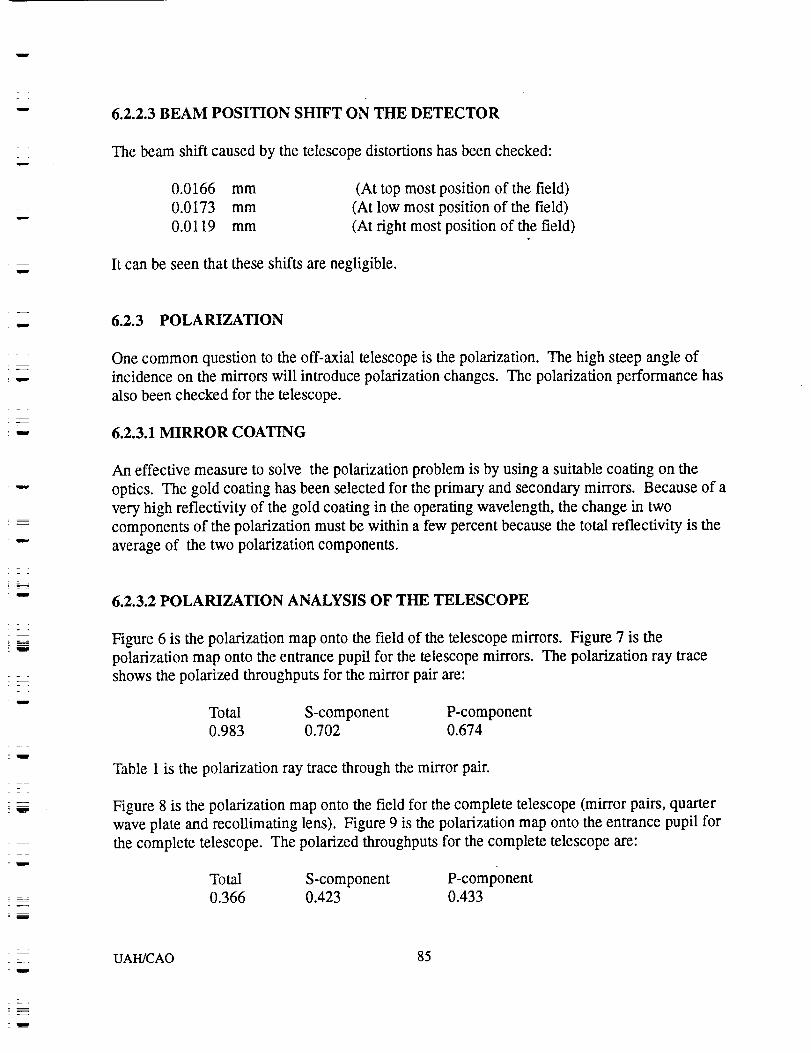
w
m
w
6.2.2.3 BEAM POSITION SHIFT ON THE DETECTOR
The beam shift caused by the telescope distortions has been checked:
0.0166 mm
0.0173 mm
0.0119 mm
(At top most position of the field)
(At low most position of the field)
(At right most position of the field)
It can be seen that these shifts are negligible.
w
m
w
m
w
w
w
6.2.3 POLARIZATION
One common question to the off-axial telescope is the polarization. The high steep angle of
incidence on the mirrors will introduce polarization changes. The polarization performance has
also been checked for the telescope.
6.2.3.1 MIRROR COATING
An effective measure to solve the polarization problem is by using a suitable coating on the
optics. The gold coating has been selected for the primary and secondary mirrors. Because of a
very high reflectivity of the gold coating in the operating wavelength, the change in two
components of the polarization must be within a few percent because the total reflectivity is the
average of the two polarization components.
6.2.3.2 POLARIZATION ANALYSIS OF THE TELESCOPE
Figure 6 is the polarization map onto the field of the telescope mirrors. Figure 7 is the
polarization map onto the entrance pupil for the telescope mirrors. The polarization ray trace
shows the polarized throughputs for the mirror pair are:
Total S-component P-component0.983 0.702 0.674
Table 1 is the polarization ray trace through the mirror pair.
Figure 8 is the polarization map onto the field for the complete telescope (mirror pairs, quarter
wave plate and recollimating lens). Figure 9 is the polarization map onto the entrance pupil for
the complete telescope. The polarized throughputs for the complete telescope are:
Total S-component P-component0.366 0.423 0.433
_ UAH/CAO 85
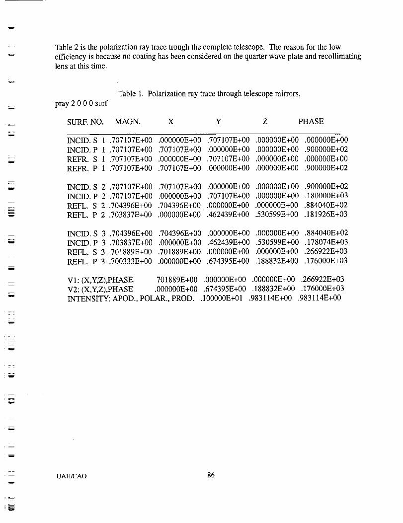
w
=
Table 2 is the polarization ray trace trough the complete telescope. The reason for the low
efficiency is because no coating has been considered on the quarter wave plate and recollimating
lens at this time.
pray 2 0 0 0 surf
Table 1. Polarization ray trace through telescope mirrors.
SURE NO. MAGN. X Y Z PHASE
=w
w
w
w
= =
w
z :
w
INCID. S 1 .707107E+00 .000000E+00 .707107E+00 .000000E+00 .000000E÷00
INCID. P 1 .707107E+00 .707107E+00 .000000E+00 .000000E+00 .900000E+02
REFR. S 1 .707107E+00 .000000E+00 .707107E+00 .000000E+00 .000000E+00
REFR. P 1 .707107E+00 .707107E÷00 .000000E÷00 .000000E+00 .900000E+02
INCID. S 2 .707107E+00 .707107E+00 .000000E+00 .000000E+00 .900000E+02
INCID. P 2 .707107E+00 .000000E+00 .707107E+00 .000000E+00 . 180000E+03
REFL. S 2 .704396E+00 .704396E+00 .000000E+00 .000000E+00 .884040E+02
REFL. P 2 .703837E+00 .000000E+00 .462439E+00 .530599E+00 .181926E+03
INCID. S 3 .704396E+00 .704396E+00 .000000E+00 .000000E+00 .884040E+02
INCID. P 3 .703837E+00 .000000E+00 .462439E+00 .530599E+00 .178074E+03
REFL. S 3 .701889E+00 .701889E+00 .000000E+00 .000000E+00 .266922E+03
REFL. P 3 .700333E+00 .000000E+00 .674395E+00 .188832E+00 .176000E+03
VI: (X,Y,Z),PHASE. 701889E+00
V2: (X,Y,Z),PHASE .000000E+00
INTENSITY: APOD., POLAR., PROD.
.000000E+00
.674395E+00
.100000E+01
.000000E+00
•188832E+00
.983114E+00
.266922E+03
.176000E+03
.983114E+00
w
m
UAH/CAO 86
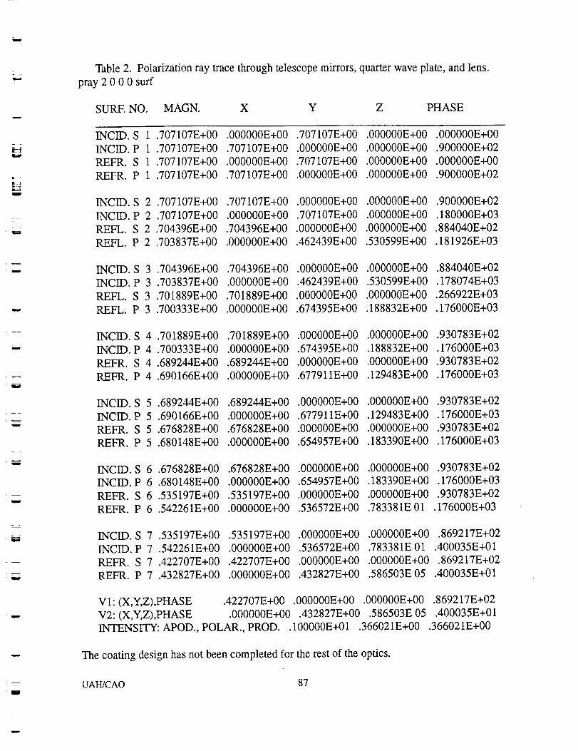
Table2. Polarizationray tracethroughtelescopemirrors,quarterwaveplate,andlens.pray2 0 0 0 surf
SURENO. MAGN. X Y Z PHASE
W
U
I
w
w
i
INCID. S 1 .707107E+00 .000000E+00 .707107E+00 .000000E+00 .000000E+00
INCID. P 1 .707107E+00 .707107E+00 .000000E+00 .000000E+00 .900000E+02
REFR. S 1 .707107E+00 .000000E+00 .707107E+00 .000000E+00 .000000E+00
REFR. P 1 .707107E+00 .707107E+00 .000000E+00 .000000E+00 .900000E+02
INCID. S 2 .707107E+00 .707107E+00 .000000E+00 .000000E+00 .900000E+02
INCID. P 2 .707107E+00 .000000E+00 .707107E+00 .000000E+00 .180000E+03
REFL. S 2 .704396E+00 .704396E+00 .000000E+00 .000000E+00 .884040E+02
REFL. P 2 .703837E+00 .000000E+00 .462439E+00 .530599E+00 .181926E+03
INCID. S 3 .704396E+00 .704396E+00 .000000E+00 .000000E+00 .884040E+02
INCID. P 3 .703837E+00 .000000E+00 .462439E+00 .530599E+00 .178074E+03
REFL. S 3 .701889E+00 .701889E+00 .000000E+00 .000000E+00 .266922E+03
REFL. P 3 .700333E+00 .000000E+00 .674395E+00 .188832E+00 .176000E+03
INCID. S 4 .701889E+00 .701889E+00 .000000E+00 .000000E+00 .930783E+02
INCID. P 4 .700333E+00 .000000E+00 .674395E+00 .188832E+00 .176000E+03
REFR. S 4 .689244E+00 .689244E+00 .000000E+00 .000000E+00 .930783E+02
REFR. P 4 .690166E+00 .000000E+00 .677911E+00 .129483E+00 .176000E+03
INCID. S 5 .689244E+00 .689244E+00 .000000E+00 .000000E+00 .930783E+02
INCID. P 5 .690166E+00 .000000E+00 .677911E+00 .129483E+00 .176000E+03
REFR. S 5 .676828E+00 .676828E+00 .000000E+00 .000000E+00 .930783E+02
REFR. P 5 .680148E+00 .000000E+00 .654957E+00 .183390E+00 .176000E+03
INCID. S 6 .676828E+00 .676828E+00 .000000E+00 .000000E+00 .930783E+02
INCID. P 6 .680148E+00 .000000E+00 .654957E+00 .183390E+00 .176000E+03
REFR. S 6 .535197E+00 .535197E+00 .000000E+00 .000000E+00 .930783E+02
REFR. P 6 .542261E+00 .000000E+00 .536572E+00 .783381E 01 .176000E+03
INCID. S 7 .535197E+00 .535197E+00 .000000E+00 .000000E+00 .869217E+02
INCID. P 7 .542261E+00 .000000E+00 .536572E+00 .783381E 01 .400035E+01
REFR. S 7 .422707E+00 .422707E+00 .000000E+00 .000000E+00 .869217E+02
REFR. P 7 .432827E+00 .000000E+00 .432827E+00 .586503E 05 .400035E+01
VI" (X,Y,Z),PHASE .422707E+00 .000000E+00 .000000E+00 .869217E+02
V2: (X,Y,Z),PHASE .000000E+00 .432827E+00 .586503E 05 .400035E+01
INTENSITY: APOD., POLAR., PROD.. 100000E+01 .366021E+00 .366021E+00
The coating design has not been completed for the rest of the optics.
UAH/CAO 87
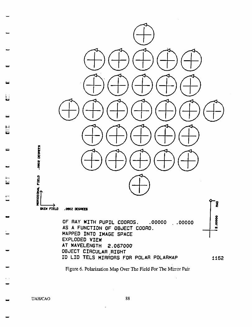
w
m
N
B
W
i
w
OF RAY NITH PUPIL COORDS. .00000
AS A FUNCTION OF OBJECT COORO.
MAPPED INTO IMAGE SPACE
EXPLODED VIEN
AT WAVELENGTH 2.067000
OBJECT CIRCULARRIGHTIO LID TELS MIRRORS FOR POLAR POLARMAP
.00000 |
1162
Figure 6. Polarization Map Over The Field For The Mirror Pair
UAH/CAO 88
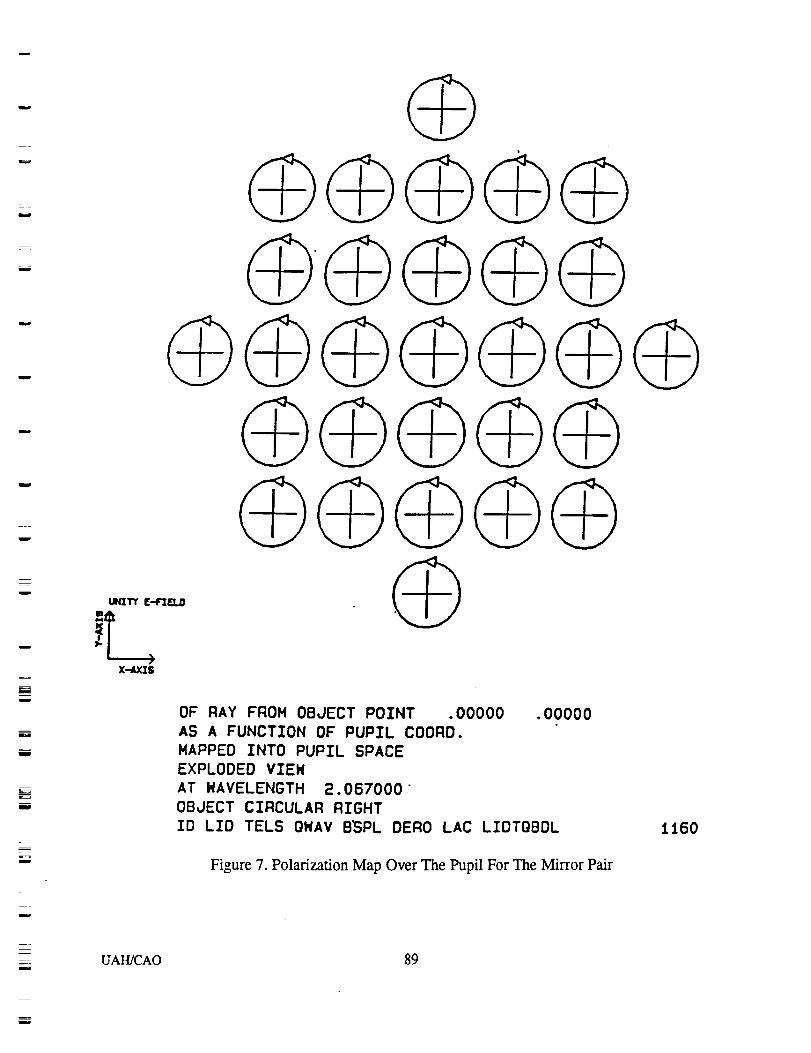
m
u
w
w
w
m
i
i
u
u
x.-_ua$
OF RAY FROM OBJECT POINT .00000
AS A FUNCTION OF PUPIL COORD.
MAPPED INTO PUPIL SPACE
EXPLODED VIEH
AT WAVELENGTH 2.067000"
OBJECT CIRCULAR RIGHT
ID LID TELS OWAV BSPL DERO LAC LIDTQBDL
.00000
Figure 7. Polarization Map Over The Pupil For The Mirror Pair
ii60
E
m
UAH/CAO 89
m
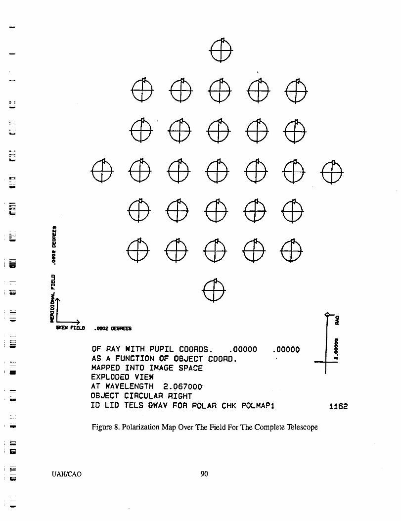
w
U
w
U
w
m
i
g
W
i
u
m
fI[:.O
UAH/CAO
eeeeeee'eeee
eeeeeeeeee
OF RAY NITH PUPIL COORDS. .00000
AS A FUNCTION OF OBJECT COORD.
MAPPED INTO IMAGE SPACE
EXPLODED VIEN
AT _AVELENGTH 2.067000"
OBJECT CIRCULAR RIGHT
IO LID TELS QWAV ffOR POLAR CHK POLMAPI
.00000
Figure 8. Polarization Map Over The Field For The Complete Telescope
90
L162
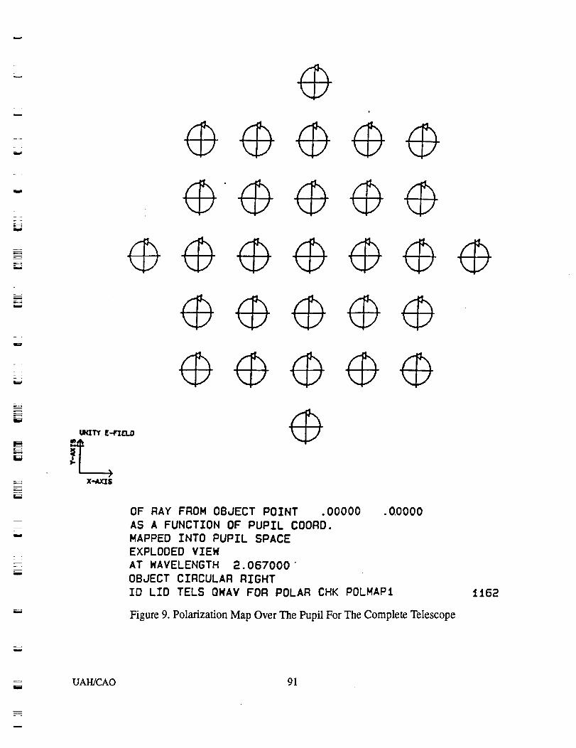
_ @eeee- eeeee_ eeeeee- eeeee1iF
eeeeee
m
X--AXIS
OF RAY FROM OBJECT POINT .00000 .0.0000
AS A FUNCTION OF PUPIL COORD.
-- MAPPED INTO PUPIL SPACE
EXPLODED VIEN
AT WAVELENGTH 2.067000 "
OBJECT CIRCULAR RIGHTID LID TELS ONlY FOR POLAR CHK POLMAPI
i
Figure 9. Polarization Map Over The Pupil For The Complete Telescope
1162
w
UAH/CAO 91
m
6.3 SENSITIVITY ANALYSIS
r
w
w
=!
w
w
u
zv :
Sensitivities for each part of the optical system have been checked by varying one parameter at a
time in the complete system to evaluate its effect on the overall performance. The performance
degradations are rms wave front error, boresight error, and beam shift on the detector. The wave
front errors are in wave at 2.067 micron. The boresight errors are in micro-radians in the object
space. The beam shift errors are in mm at the detector surface. The parametric errors are
decenters, tilts, thickness error, and wedge error for each optical element. The decenter and
thickness errors are in mm, while the tilt and wedge errors are in milli-radians.
Table 3 lists all the sensitivities with parametric errors and the corresponding performance errors.
The sensitivities which are not listed are much looser than 1 mm in length and 1 milli-radians in
angle.
6.3.1 PRIMARY AND SECONDARY MIRRORS
Because of the non-symmetrical nature of the off-axis telescope, all six parametric errors are
independent for each mirror. The linear displacement errors are on the order of 0.01 mm and
contribute a little over 1/10 wave rms wave front errors. The angular errors are on order of 0.01
milli-radians for the primary and 0.10 milli-radians for the secondary to introduce a little under
1/10 wave rms wave front errors. Some numbers are not symmetrical in sign. The most sensitive
values are listed for these non-symmetrical parameters. The most sensitive displacement is the
axial spacing. A 0.01 mm axial position change for the secondary mirror will introduce a 0.161wave rms wave front error. The most sensitive tilt is the tilt around x-axis. A 0.01 milli-radians
change in the primary mirror will introduce a 0.056 wave rms wavefront error.
The secondary mirror has been designed to have lower tilt sensitivities are lower because it is
difficult to maintain the angular position to tight tolerances on a small mirror.
6.3.2 QUARTER WAVE PLATE
The quarter wave plate will introduce errors because it is located in the convergent ray path. The
quarter wave plate is simply a plate with a symmetrical shape. Only tilt, thickness, and wedgeerrors have been checked. The thickness error of 0.01 mm will introduce a 0.079 wave rms wave
front error. A 10.0 milli-radians of tilt and 1.0 milli-radians rotation will introduce 0.022 wave and
0.061 wave rms wave front error respectively.
The axial location of the quarter wave plate almost has no effect on the performance.
6.3.3 COLLIMATING LENS
The collimating lens is also working at off-axis. All six possible variations have been checked.
As compared to the primary and secondary mirrors, the collimating lens has much lower
sensitivities. The axial displacement of 0.01 mm will introduce a 0.023 wave rms wavefront error.
UAH/CAO 92
w
I
w
m_
w
_L
In real practice, this axial displacement can be used to fine tune the wavefront performance to
compensate for the errors caused by the element fabrication, assembly and alignment. The
in-plane location of the lens has a range of 0.1 mm. Tilts are of the order of 1.0 milli-radians.
The in plane rotation can be 10.0 milli-radians. The wedge in two directions is 1.00 milli-radians.
The reason for lower sensitivities of the lens as compared to the mirror is that the two surfaces of
the lens are close a parallel surface. When both surfaces are displaced together, the effects are
partly canceled.
6.3.4 CUBIC BEAMSPLITTER
A cubic beamsplitter is located in the collimated beam path. The effect on the wave front
performance is very low just as for the rest of the optical parts. However, any changes in these
parts will introduce a boresight error or a beam shift on the detector. A thickness change of 1.00
mm will introduce a 0.011 mm beam position on the final detector.
The effect of the beamsplitter position error is essentially none.
6.3.5 BEAM DEROTATOR
The axial position of the derotator will introduce a beam shift only. A 1.00 mm of axial
displacement will create a 0.037 mm beam shift on the detector. The thickness of the derotator
also introduces a beam shift. In real practice, the axial position of the derotator can be used to
compensate for the fabrication error of the derotator thickness. A tilt change in the derotator only
introduces a boresight error. The wedge angle also introduces a boresight error. Again, the tilt
angle can be used to compensate for the fabrication error of the derotator wedge. The
synchronous error (clocking angle) of 1.00 milli-radiance of the derotator will introduce a 1.400
micron radians of the boresight error in the object space. The center of the derotator should be on
the center of the beam. Any error in the axis offset will cause a residual beam shift in the same
amount.
6.3.6 LAG ANGLE COMPENSATOR
The lag angle compensator is a simple flat mirror. A change of 0.01 mm in the normal position of
this mirror surface will introduce a 0.014 mm beam position on the detector. The two directional
flits will introduce a boresight change of 0.56 micron radians and 0.8 micron-radians respectively
for a 0.01 milli-radians changes in the tilt angle. These two ratios are the angular transfer function
of the lag angle compensator needed for programming of the lag angle compensator controller.
All sensitivities are the effects of one parameter at a time. The combination of the errors needs a
more detailed modeling. One simple estimate can be made based on statistically reducing the
values by square root of the number of the dominant variables. The dominant variables are those
which are hard to fabricate or align.
UAH/CAO 93
JJ
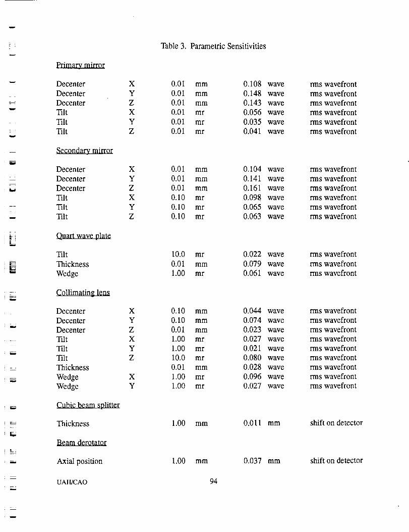
=
w
r_
I
, r _
w
L
E_
i
i
i
m
__=
w
m
i
Primary. mirror
Decenter
Decenter
Decenter
Tilt
Tilt
Tilt
Secondary mirror
Decenter
Decenter
Decenter
Tilt
Tilt
Tilt
Quart wave plate
Tilt
Thickness
Wedge
CoUimatin_ lens
Decenter
Decenter
Decenter
Tilt
TiltTilt
Thickness
Wedge
Wedge
Cubic beam splitter
Thickness
Beam derotator
Axial position
UAH/CAO
Table 3. Parametric Sensitivities
X 0.01 mm 0.108
Y 0.01 mm 0.148
Z 0.01 mm 0.143
X 0.01 mr 0.056
Y 0.01 mr 0.035
Z 0.01 mr 0.041
X 0.01 mm 0.104
Y 0.01 mm 0.141
Z 0.01 mm 0.161
X 0.10 mr 0.098Y 0.10 mr 0.065
Z 0.10 mr 0.063
10.0 mr 0.022
0.01 mm 0.0791.00 mr 0.061
X 0.10 mm 0.044
Y 0.10 mm 0.074Z 0.01 mm 0.023
X 1.00 mr 0.027
Y 1.00 mr 0.021
Z 10.0 mr 0.080
0.01 mm 0.028
X 1.00 mr 0.096
Y 1.00 mr 0.027
1.00 mm 0.011
1.00 mm 0.037
94
wave
wave
wave
wave
wave
wave
wave
wave
wave
wave
wave
wave
wave
wave
wave
wave
wave
wave
wave
wave
wave
wave
wave
wave
mm
mm
rms wavefront
rms wavefront
rms wavefront
rms wavefront
rms wavefrontrms wavefront
rms wavefront
rms wavefront
rms wavefront
rms wavefront
rms wavefront
rms wavefront
rms wavefront
rms wavefrontrms wavefront
rms wavefront
rms wavefront
rms wavefront
rms wavefront
rms wavefront
rms wavefront
rms wavefront
rms wavefront
rms wavefront
shift on detector
shift on detector
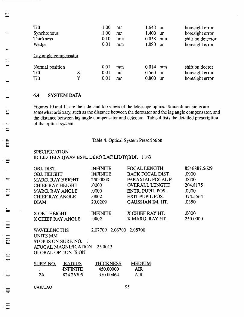
w
w
w
w
w
w
=,
_____
w
m
m
m
Tilt 1.00 mr 1.640 lar boresight error
Synchronous 1.00 mr 1.400 _ boresight errorThickness 0.10 mm 0.058 mm shift on detector
Wedge 0.01 mm 1.880 I.tr boresight error
Lag angle compensator
Normal position 0.01 mm 0.014 mm shift on doctor
Tilt X 0.01 mr 0.560 gr boresighterror
Tilt Y 0.01 mr 0.800 _ boresight error
6.4 SYSTEM DATA
Figures 10 and 11 are the side and top views of the telescope optics. Some dimensions are
somewhat arbitrary, such as the distance between the derotator and the lag angle compensator, and
the distance between lag angle compensator and detector. Table 4 lists the detailed prescription
of the optical system.
Table 4. Optical System Prescription
SPECIFICATION
ID LID TELS QWAV BSPL DERO LAC LIDTQBDL 1163
OBJ. DIST.
OBJ. HEIGHT
MARG. RAY HEIGHT
CHIEF RAY HEIGHT
MARG. RAY ANGLE
CHIEF RAY ANGLE
DIAM
INFINITE FOCAL LENGTH 8546887.5629
INFINITE BACK FOCAL DIST. .0000
250.0000 PARAXIAL FOCAL R .0000
.0000 OVERALL LENGTH 204.8175
.0000 ENTR. PUPIL POS. .0000
.0802 EXIT PUPIL POS. 374.5564
20.0209 GAUSSIAN IM. HT. .0350
X OBJ. HEIGHT
X CHIEF RAY ANGLE
INFINITE X CHIEF RAY HT. .0000
.0802 X MARG. RAY HT. 250.0000
WAVELENGTHS 2.07700 2.06700
UNITS MM
STOP IS ON SURF. NO. 1
AFOCAL MAGNIFICATION 25.0013
GLOBAL OPTION IS ON
2.05700
SURF. NO. RADIUS
1 INFINITE 450.00000
2A 824.26305 350.00464
MEDIUMAIR
AIR
UAH/CAO 95
w
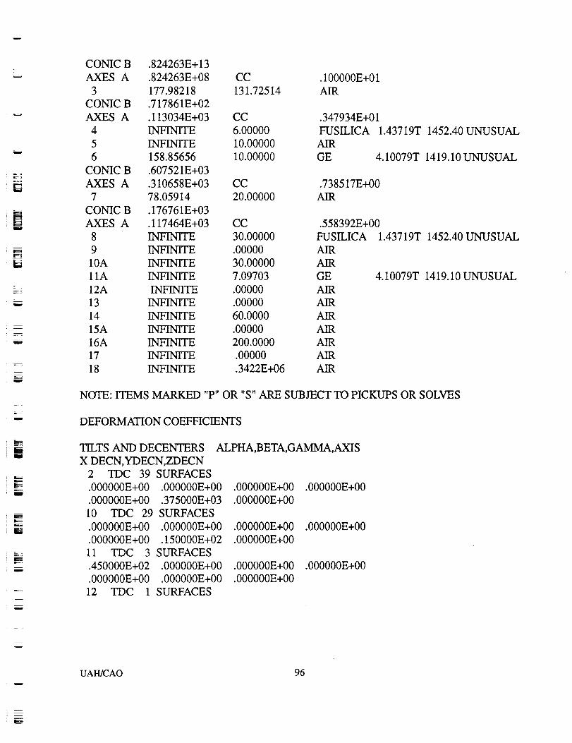
= :
7w
m
_z
x_
w
N
N--=
CONIC B .824263E+13
AXES A .824263E+08 CC
3 177.98218 131.72514
CONIC B .717861E+02
AXES A .113034E+03 CC
4 INFINITE 6.00000
5 INFINITE 10.00000
6 158.85656 10.00000
CONIC B .607521E+03
AXES A .310658E+03 CC
7 78.05914 20.00000
CONIC B .176761E+03
AXES A .117464E+03 CC
8 INFINITE 30.00000
9 INFINITE .00000
10A INFINY_ 30.00000
11A INFINY_ 7.09703
12A INFINITE .00000
13 INFINITE .00000
14 INFINITE 60.0000
15A INFINITE .00000
16A INFINITE 200.0000
17 INFINITE .00000
18 INFINITE .3422E+06
.100000E+01
AIR
.347934E+01
FUSILICA 1.43719T 1452.40 UNUSUAL
AIR
GE 4.10079T 1419.10UNUSUAL
.738517E+00
AIR
.558392E+00
FUSILICA 1.43719T
AIR
AIR
GE 4.10079T
AIR
AIR
AIR
AIR
AIR
AIR
AIR
1452.40UNUSUAL
1419.10UNUSUAL
NOTE: ITEMS MARKED "P" OR "S" ARE SUBJECT TO PICKUPS OR SOLVES
DEFORMATION COEFFICIENTS
TILTS AND DECENTERS
X DECN,YDECN,ZDECN
ALPHA,BETA,GAMMA,AXIS
2 TDC 39 SURFACES
.000000E+00 .000000E+00 .000000E+00 .000000E+00
.000000E+00 .375000E+03 .000000E+00
10 TDC 29 SURFACES
.000000E+00 .000000E+00 .000000E+00 .000000E+00
.000000E+00 .150000E+02 .000000E+00
11 TDC 3 SURFACES
.450000E+02 .000000E+00 .000000E+00 .000000E+00
.000000E+00 .000000E+00 .000000E+00
12 TDC 1 SURFACES
w
w
UAH/CAO 96
m
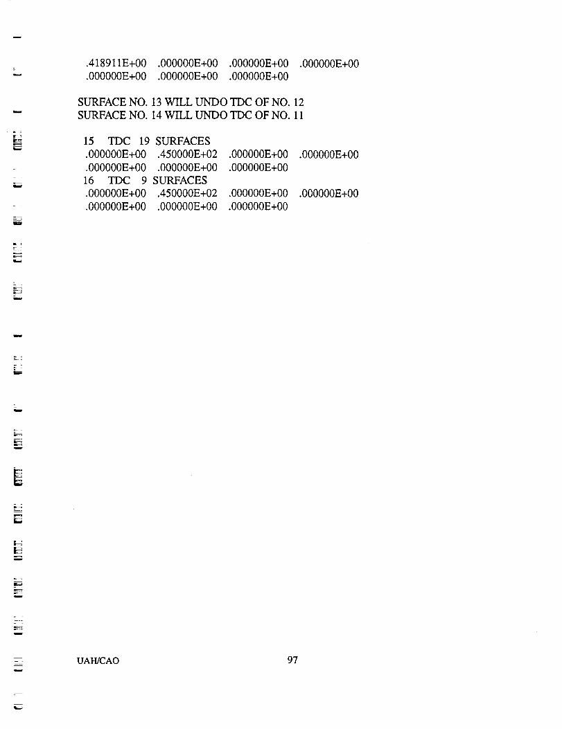
.418911E+00 .000000E+00 .000000E+00 .000000E+00
.000000E+00 .000000E+00 .000000E+00
SURFACE NO. 13 WILL UNDO TDC OF NO. 12
SURFACE NO. 14 WILL UNDO TDC OF NO. 11
15 TDC 19 SURFACES
•000000E+00 .450000E+02 .000000E+00 .000000E+00
.000000E+00 .000000E+00 .000000E+00
16 TDC 9 SURFACES
.000000E+00 .450000E+02 .000000E+00 .000000E+00
.000000E+00 .000000E+00 .000000E+00
L
_7
i
z
W
F_i
w
w
w
UAH/CAO 97
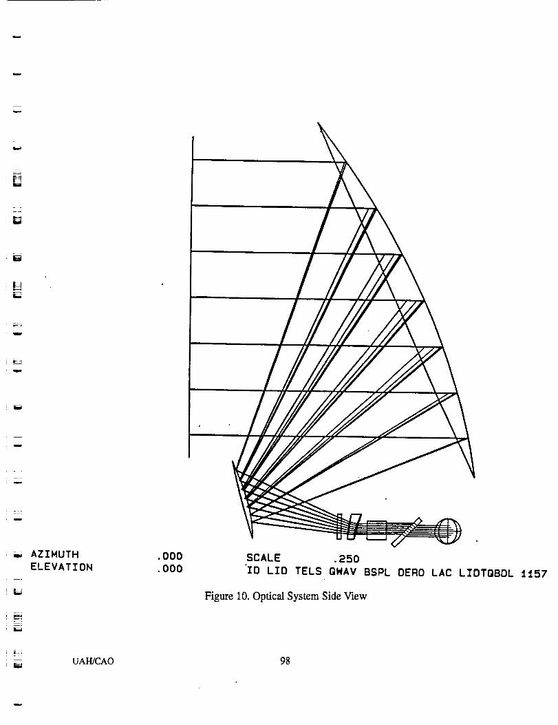
w
W
U
L_
r
!
w
=-_..AZIMUTH .000
ELEVATION .000
UAH/CAO
SCALE .250
IO LID TELS QNAV BSPL OERO LAC LIDTQBOL _57
Figure 10. Optical System Side View
98
w
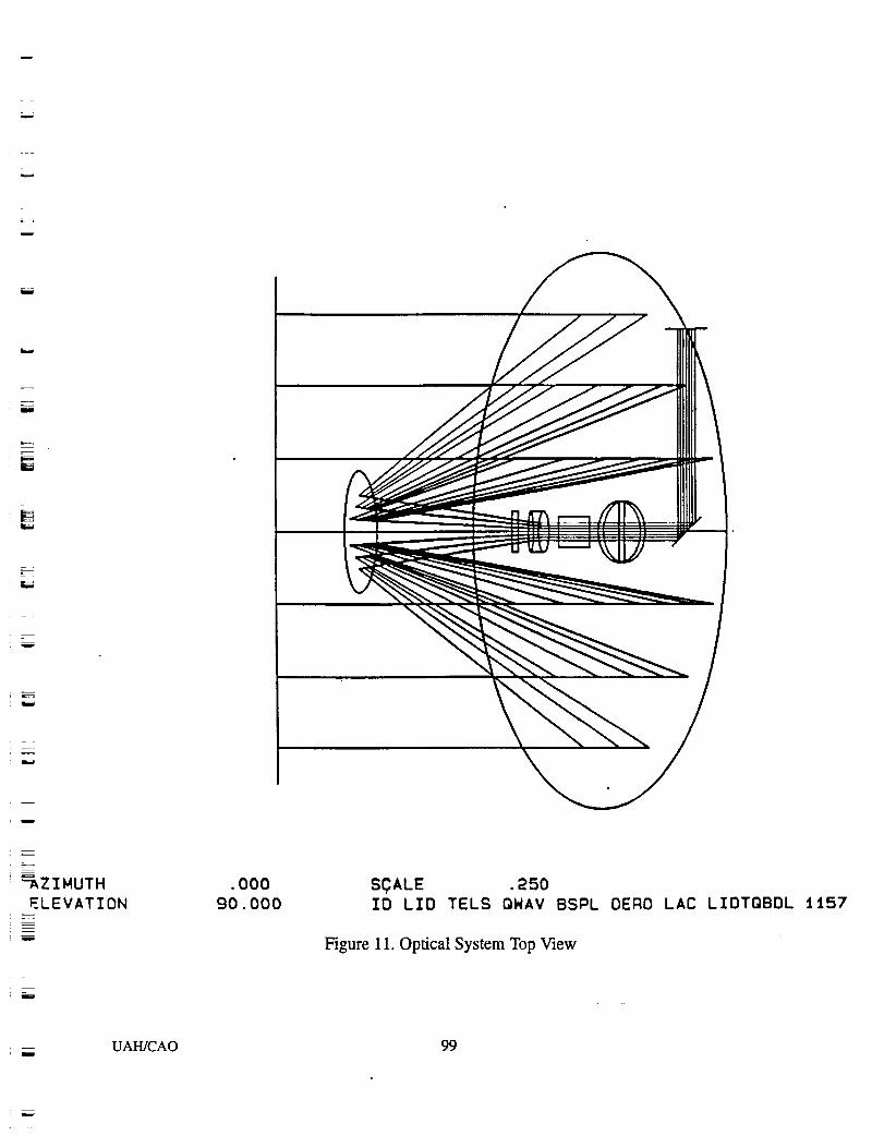
Ew
W
i
mw
W
w
_ZIMUTH
ELEVATION
.000
90.000SCALE .250TO LID TELS QWAV BSPL OERO LAC LIDTOBDL _C57
Figure 11. Optical System Top View
w
wUAI-UCAO 99
mw
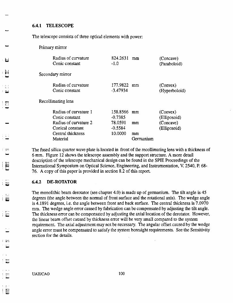
6.4.1 TELESCOPE
The telescope consists of three optical elements with power:
Primary mirror
Radius of curvature 824.2631 mm
Conic constant - 1.0
Secondary mirror
Radius of curvature
Conic constant
(Concave)
(Paraboloid)
Recollimating lens
Radius of curvature 1
Conic constant
Radius of curvature 2
Conical constant
Central thickness
Material
177.9822 mm (Convex)
-3.47934 (Hyperboloid)
158.8566 mm (Convex)
-0.7385 (Elliposoid)
78.0591 mm (Concave)
-0.5584 (Elliposoid)
10.0000 mm
Germanium
w
z
_E
--4
m
i
!
i
The fused silica quarter wave plate is located in front of the recol!imating lens with a thickness of
6 mm. Figure 12 shows the telescope assembly and the support structure. A more detail
description of the telescope mechanical design can be found in the SPIE Proceedings of the
International Symposium on Optical Science, Engineering, and Instrumentation, V. 2540, P. 68-
76. A copy of this paper is provided in section 8.2 of this report.
6.4.2 DE-ROTATOR
The monolithic beam derotator (see chapter 4.0) is made up of germanium. The tilt angle is 45
degrees (the angle between the normal of front surface and the rotational axis). The wedge angle
is 4.1891 degrees, i.e. the angle between front and back surface. The central thickness is 7.0970
mm. The wedge angle error caused by fabrication can be compensated by adjusting the tilt angle.
The thickness error can be compensated by adjusting the axial location of the derotator. However,
the linear beam offset caused by thickness error will be very small compared to the system
requirement. The axial adjustment may not be necessary. The angular offset caused by the wedge
angle error must be compensated to satisfy the system boresight requirements. See the Sensitivitysection for the details.
i
UAH/CAO 100
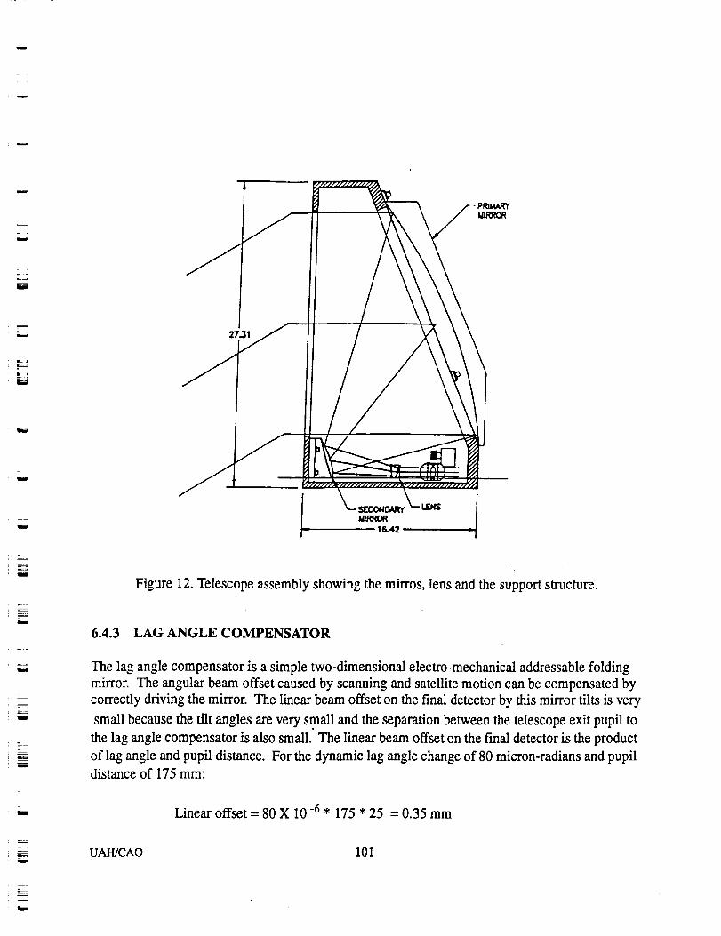
= ,
m
W
w
w
J
__=
m
m
m
Figure 12. Telescope assembly showing the mirros, lens and the support structure.
6.4.3 LAG ANGLE COMPENSATOR
The lag angle compensator is a simple two-dimensional electro-mechanical addressable folding
mirror. The angular beam offset caused by scanning and satellite motion can be compensated by
correctly driving the mirror. The linear beam offset on the final detector by this mirror tilts is very
small because the tilt angles are very small and the separation between the telescope exit pupil to
the lag angle compensator is also small.' The linear beam offset on the final detector is the product
of lag angle and pupil distance. For the dynamic lag angle change of 80 micron-radians and pupil
distance of 175 mm:
Linear offset = 80 X 10 -6,175 * 25 = 0.35 mm
UAH/CAO 101
w
Where 25 is the telescope magnification. The linear bean offset is only 1.75 % of the 20 mm
beam diameter.
w
--=
w
The transfer functions of the lag angle compensator are linear factors of 0.71429 and 0.5 (ratio of
mirror tilt and beam deviation) for the horizontal and vertical directions respectively. The tilt
ranges for the 80 micro radians dynamic lag angle are:
Horizontal range = 0.71429 * 80 * 25 = 1.4286 milliradians
Vertical range = 0.5 * 80 * 25 = 1.0 miUiradians
The accuracy of the mirror positions for the 1 micro radians of system boresight requirement are:
Horizontal range = 0.71429 * 1 * 25 = 17.8573 micro radians
w
Vertical range = 0.5 * 1 * 25 = 12.5 micro radians
The swing rates of the mirrors for the 160 microseconds pulse reception time are:
Horizontal rate = 0.001429 / 0.00016 = 8.931 radians/second
w
Vertical rate = 0.001 / 0.00016 = 6.25 radians/second
w 6.0 RECOMMENDED FURTHER WORK ON OPTICAL SUBSYSTEM
m
=, =
m
A preliminary analysis was performed on the performance and tolerances for a 250 mm version of
the telescope described in this chapter. The results of this analysis indicate that a 250 mm tele-
scope will have the same type of fabrication and alignment tolerances as the 500 mm telescope.
For a 250 mm telescope, the decenter tolerances are basically identical to those of the 500 mm
telescope. But the tilt tolerances mostly increase for the 250 mm telescope. To fully predict the
250 mm telescope performance and to determine its tolerances, some additional work is required.
Other recommended future work include a complete coating design is needed for all the elements.
Upon completion of the coating design, a detail polarization analysis is necessary to accurately
determine the effects of the optical subsystem on the lidar overall performance. Excess scattering
of the transmitter beam off the optical components may disrupt the operation of the lidar detector.
Therefore, a scattering analysis must be performed to determine the level of the scattered laser
beam radiation that is collected by the heterodyne receiver. Finally, it is recommended to perform
a complete system performance modeling and analysis to allow the lidar design optimization.
UAH/CAO 102
7.0 L1DAR COMPUTER DATABASE AND
WORLD WIDE WEB SERVER
w
w
!
w
L =
w
w
N
[]
==
The NASA/MSFC lidar computer database, previously developed the UAH personnel, was
upgraded and a large number (>400) of lidar related materials were added to the database.
After completing the entry of all the lidar related materials in the MSFC/EO Branch into the
database, the other sources of lidar materials within MSFC were identified. Most of these
materials were added to the database bringing the total number of entries to more than 1750
items which include about 1230 journals, 460 reports and technical memorandums, and 60
books, theses and proposals. The database software was further enhanced by incorporating an
automatic file folder label generator for all new database entries. In addition, a page scanner
hardware and an Optical Character Recognition (OCR) software were installed to improve the
data entry process. This scanner system will also support the World Wide Web (WW server
development effort.
A WWW server was developed to familiarize the industry, academic and other government
agencies with the MSFC coherent lidar activities and to provide them with an efficient means of
accessing the E-O branch information base through computer networks. The Hyper Text Transfer
Protocol (HTTP) server software, developed by the National Center for Supercomputing
Applications (NCSA), was installed on a PC dedicated to the WWW. Both SUN PC-NFC and
Novell LAN Workplace networking software were evaluated for interfacing with the internet. The
Novell LAN Workplace was then selected and installed on the PC. The server was then tested
using NCSA Mosaic on different SUN SPARC stations and a MacIntosh computer to ensure
proper transfer of information through the internet and the document format compatibility with
different computers. After some modifications, it was shown that the server can be run at near
full capacity. A great deal of materials relating to the E-O branch and the coherent lidar field have
been placed on the server. These materials were prepared specifically for the WWW by the
members of E-O branch and the UAH personnel. The server documents, which include text,
mathematical expressions and images, were first transferred to the PC and then edited and
converted to the proper format for the server using HTML Assistant word processor. The
documents that are presently available on the server include: tutorials on coherent lidar technique
and its applications, some of the current activities and projects, past accomplishments, a recent
review paper that appeared at a SPIE proceeding, and spin-off technologies. The breakdown of
the MSFC electro-optics branch WWW server are as following:
• 84 HTML documents 205 KB
• 20 in-lined GIF images 315 KB
• 20/PEG images 1.60 MB
• Total 2.10 MB
In order to accommodate for the increasing number accesses and links to other severs, and to
allow the addition of more documents, and to provide a reliable and uninterrupted service, the
server computer was upgraded from a 386SX25 machine with 4 MB of RAM to a 486DX66 with
16 MB of RAM. The server resource configuration was then modified to take advantage of more
UAH/CAO 103

r_
!
m
w
available memory and to increase the speed of the server in responding to its users and fulfilling
their requests. The UAH personnel also monitored the server traffic and maintained statistical
record on the server usage on the daily basis. A backup procedure was also developed to
regularly store the server documents to data tapes as an added precaution for uninterrupted service
to the interested organizations throughout the world.
8.0 RELATED ACTIVITIES
8.1 NASA SENSOR AND NOAA SPACE-BASED LIDAR WORKING GROUP
MEETINGS
UAH personnel attended the NASA Sensor Working Group Meeting on September 21-22, 1994 in
New Carrollton, MD. In this meeting, the capabilities of the DCF and the status of its
development was presented and the results of the measurements performed in the companion
Laser Characterization Facility (LCF) on a 2-micron coherent lidar transceiver, developed by the
U.S. Air Force, were described. UAH personnel also participated in a technical coordination
meeting for the NASA solid state coherent lidar program at MSFC on November 15, 1994. In
addition to MSFC and UAH, this meeting was attended by representatives from Jet Propulsion
Laboratory and the Langley Research Center.
UAH personnel attended two Meetings of the NOAA Working Group on Space-Based Lidar
Winds in Clearwater, Florida (January 31-February 2, 1995) and in Frisco, Colorado (July 19-21,
1995). The status of the NASA/MSFC and UAH 2-micron solid state coherent lidar efforts were
described in these meetings.
u8.2 CONFERENCES
m
m
w
Three conference papers, describing some of the work performed under this deliver order, were
prepared and presented at the SPIE International Symposium on Optical Science, Engineering,
and Instrumentation, in San Diego, California, July 9-14, 1995 AND the Coherent Laser Radar
Topical Meeting in Keystone, Colorado, July 23-27, 1995. The followings provide the summaries
of these papers.
L
w
w
UAH/CAO 104
w
w
w
w
m
U
w
r_
w
w
=- ___
SPIE Int. Symposium on Opt. Sci., Eng_n., and Instrumentatign San Deigo, CA., July 9-14 1995Design and analysis ofa spaceborne lidar telescope
Chen Feng, Anees Ahmad and Far-zin Amzajerdian
Center for Applied OpticsThe University of Alabama in Huntsville
Huntsville, AL35899
ABSTRACT
A spacebome telescope has been designed and analyzed for a 2-micron solid state coherent lidar system operating on a satellite.
The optical system consists of a large off-axis reflective telescope, a large-aperture diffractive scanner, an image derotator and
a 14 angle compensator. Due to the orbiting motion of the satellite and scanning, the boresight of the telescope shifts duringthe round trip travel time of the'laser pulses to the target, ha a coherent lidar system utilizing optical heterodyne detection, the
relative alignment of the received signal with respect to the local oscillator beam is particularly critical. Two compensators have
been designed to correct the boresight errors as well as the wavefront errors caused by beam wandering due to the boresight
changes. Several design approaches for the compensators have been investigated. The optical and optomechanical design
issues for such a system are discussed. The results of optical performance, modeling and tolerance analysis for the telescopeare also presented.
Kevwords: optical desi_ and modeling, large reflective optics, diffractive optics, tolerance analysis, boresight shiftcompensation, lidar, coherent laser radar, satellite
1. INTRODUCTION
Several studies have indicated that the optimum approach to measure atmospheric wind from space is a pulsed coherent [idar'.:.
However, these studies recommended a pulsed CO2 laser radar system, operating at ! 0 micron wavelength with a pulse energy
of near 20 J, pulse repetition frequency (PRF) of about 5 Hz, optical aperture of approximately !.6 m, and full-time operation
(100% on- orbit duty cycle). These requirements are too expensive. The size, weight, and energy consumption for such a
system are beyond the capability of small satellites. NASA's Marshall Space Flight Center (MSFC) has, therefore, initiated
an investigation to address innovative designs of a space-based coherent lidar system, which are smaller, lighter, less expensive,
and consume less power 3. The Center for Applied Optics (CAO) has recently conducted an optical design of the telescope and
its associated optical subsystems for the new compact coherent lidar.
The new lidar optical system consists of a holographic optical element (HOE) beam scanner, an off-axis beam expanding
telescope, a wedge derotator, and a two-dimensional lag angle compensator. The size, weight and complexity of this new
system are substantially reduced as compared to the optical systems previously proposed for a space-based coherent lidar 4.5.
In addition, the parametric sensitivities of this system design make its implementation achievable at a much reduced fabricationand integration cost.
When the various requirements of the mission that must be achieved simultaneously are considered from a system perspective,
the sensor of choice for this mission is a solid state pulsed coherent lidar operating at 2-micron wavelen=_.h. The lidar utilizesa relatively high power, pulsed laser as the transmitter and a low power, continuous-wave laser as the local oscillator source.
The transmitter laser is injection locked to produce single frequency pulses using a highly stable, single frequency, continuous-
wave, master oscillator laser. Pan of the master laser is also used for controlling the local oscillator laser frequency that varies
with the scanner position to compensate the gross spacecraft-induced Doppler frequency shift. The use of a frequency-tunable
local oscillator laser relaxes the bandwidth requirements of the lidar detector and the processing electronics.
A strnplified schematic of a pulsed coherent lidar is shown in Figure I. The pulsed laser output beam is expanded by an off-axis
telescope to be transmitted to the atmosphere. The quarter-wave plate placed along the propagation path changes the
UAH/CAO 105
68 / SPIE Vol 25400.8 _9._-1899-4/9 5/$6.00
w
w
--2
_ im
w
L_
w
W
w
w
m
w
polarization of the transmitted beam from vertical to circular. The return beam from the atmosphere is received by the same
telescope and directed through the quarter-wave plate and a polarizing beamsplitter toward the detector. The derotator and lagangle compensator (LAC) are placed along the return signal path to correct for the boresi_t and wavefront errors caused by
the scanner and spacecraft motions. At the detector, the return radiation is mixed with the local oscillator beam for heterodynedetection. The detector in turn generates an electrical signal at the difference frequency between the signal and local oscillator
frequencies. The output of the detector is then ban@ass filtered and amplified to be digitized and processed for Dopplerfrequency shift due to the atmospheric winds.
Previous work 3.6has specified the optimum laser pulse width and repetition rate at 200 nano-secords and l0 I--Izrespectively,
and has selected a telesco ,e aperture diameter of 500 ram, and a scanner half-angle of 30 degrees fc: the space-based coherent
lidar operating at 2-micron wavelength. For the purposes of this work, it has further been assumed that the spacecraft has asun-synchronous orbit at 350 km above the sea level. The measurement range has been assumed to be from the ground-levelto 20 lcm altitude.
2. OPTICAL SYSTEM DESIGN
The overall function of the coherent lidar optical system is to expand the laser beam, and direct it towards the atmosphere ina conical scan, to receive the back.scattered radiation, and compensate for the wavefront and boresight errors caused by the
scanner and spacecraft motions. The major requirements are: (I) beam expanding aperture of 500 mm; (2) input laser beamdiameter of 20 ram; (3) conical scan rate of 10 RPM; (4) nadir angle of 30 degrees; (5) no internal focal point to avoid air breakdown in ground system testing; (6) diffraction limited beam quality; (7) lag angle compensation to maintain the boresight towithin I micro-radian.
2.1 Beam expanding telescope
The beam expanding telescope is an off-axis catadiopmc system, which serves both as the transmitter laser beam expander andas the receiver collecting telescope. Various configurations for the telescope have been evaluated against the performancerequirements. An off-axis configuration has been selected to eliminate the central obscuration of an on-axis design, whichdegrades the beam quality due to the diffraction pattern of the obscuration. The off-axis configuration also effectively reduces
the backscattering of the transmitted pulses by the front surface of the telescope secondary. A Galilean type of telescope hasbeen employed to eliminate the real focus of the Keplierian type of telescope. The beam wander problem of a Galilean
telescope (because of no real exit pupil) can be solved by using additional corrective optics. A catadioptric design with arefractive exit lens has been proposed to provide enough back-relief space to accommodate the beamsplitter, derotator and lagangle compensator. Figure 2 is the layout of a compact two-mirror one lens off-axis telescope.
The two mirrors are a parabola and a hyperbola as in a standard Cassegrain type of telescope. An aspheric negative lens hasbeen used to recollimate the beam. The telescope has: (l) a field of view 0.17 degree to cover the lag angle of the return beam;(2) afocal ma_ificafion of 25X to expand the 20 mm beam to a 500 mm diameter; (3) RMS wavefi'ont error of I/l 0 wave atthe exit pupil for 2.067 micron wavelength, (4) zero obscuration and vignetting; (5) no internal real focus; and (6) a mirror
spacing of only 350 ram. Figure 3 shows the wavefront error of this telescope for the transmitted and return beams, and Figure4 shows the point spread function in the telescope exit space for both the beams.
The flat field characteristic of this telescope design eliminates the need for any additional optics to compensate for the return
beam angular deviations from the telescope optical axis that are caused by the scanner motion and lag angle. Fun.hermore, thepupil relay optics can also be omitted since the beam wander is only a few millimeters at the derotator input, which is located
about 150 mm from the telescope exit lens. Figure 5 illustrates the layout of the lidar optical system including the telescope,scanner, derotator, and lag angle compensator.
UAH/CAO 106
w
SPIE rot 2540/69
2.2 Beam scanner
A Holographic Optical Element (HOE) scanner is being considered as a lightweight alternative to a wedge or prism scanner.A germanium prism with about 9 degree wedge angle is required for deflecting the laser beam throu_ an angle of 30 de_ees.Such a prism will be quite expensive, heavy and difficult to fabricate for the required 500 mm optical aperture. Since this
application requires a simple conical scan of a monochromatic and collimated beam with a fixed deflection angle, a HOEscanner may be a viable choice. Compared with the wedge scanners, a HOE scanner will allow for much easier spacecraftaccommodation because of its lower mass and symmetrical structure. Furthermore, HOE scanners do not suffer from phasedomain limitations associated with the large diameter wedge scanners required for this application.
7_
I
Iw==_
u
i
r_
2.3 Beam derotator
The lidar scanner and platform motions during the transmitted pulse round-trip time cause the return beam to deviate from the
optical axis established by the transmitter beam. Therefore, additional optical assemblies are required to compensate for thesemotions and maintain the relative alignment of the return and local oscillator beams during the pulse reception time. The return
beam angular deviation or lag angle can be divided into two components, a dominant static component and a much smallerdynamic component. The scanner and orbital motion contn'butions to the static component of the lag angle are about 1400 and3 micro-radians, respectively, and their contributions to the dynamic component of the lag angle are 80 and 0.18 micro-radians.
The static component of the lag angle is compensated by an optical subsystem, referred to as the derotatur, and its dynamiccomponent is corrected by the lag angle compensator (LAC) subsystem.
The derotator employed i_ the earlier designs utilized a two mirror periscope that rotates with the scanning telescope to maintain
a fLxedseparation between the transmitted and return beams while eliminating the return beam motion. To furthersimplifythe optical system design and improve its robustness, a single optical wedge has been utilized to perform as the signal beamderotator. The derotator wedge is placed about 150 mm from the telescope exit lens at 45 de_ees with respect to the optical
axis. The derotator rotation is s_chronized, but 90 degrees out of phase, with respect to that of the scanner.
Since the telescope has a virtual exit pupil that is located between its secondary and exit lens, the scanner motion causes thereturn beam to rotate about the optical axis making a conical pattern with a half-angle of the order of a milli-radian at the
telescope entrance pupil. The wedge derotator then deflects and lranslates the return beam in such a manner that its propagationpath coincides with the optical axis established by the transmitted beam and extends to the center of the lidar detector.
2.4 Lag angle compensator
The return beam dynamic lag angle changes during the pulse reception the, which is about 160 microseconds. This will be
compensated by a two-axis steering LAC mirror. The LAC mirror is driven by the pointing controller in a repeating patternso that the return beam remains centered on the detector over the duration of the pulse reception. As opposed to the earlierproposed design that uses two active fold mirrors, the single mirror LAC allows certain beam wander at the telescope collectingaperture.
The lag angle compensator will take out the angular boresight error leaving the residual wavefront aberrations only. The f'Lxederrors, such as fabrication errors, system misalignment, and pans and structure distortions, can be compensated by resettingthe zero of LAC. The systematic errors, such as the telescope optical distortions and the residual lag due to the derotator, can
be compensated by adding control contributions to LAC.
3. SENSITIVITY ANALYSIS
It is eas.v to design an optical system that can never be built because of" its hi_ parametric sensitivi_ _, i.e.very ti_ht fabricationand assembly tolerances. Parametric sensitivity of the telescope has been analyzed to determine its performance for real
UAH/CAO 107
70 / 5PIE Vo/ 2540
HW
L
H
==
U
w
m_
w
m
fabrication and assembly tolerances. Table l lists the wavefront errors induced by tilts and decenters of individual elements.
Table 2 lists the boresight errors induced due to all these tolerances. The most sensitive element is the primary mirror. To
maintain 1/10 k rms wavefront and I micro-radians boresight system performance, the decenters should be less than 0.01 mm
and tilts should be less than 0.01 miIli-radians.
4. POLARIZATION
The polarization requirements for a high heterodyne efficiency can be met by using very high efficiency reflective coatings
to compensate for the phase shift caused by various coatings (particularly the dichroic beamsplitters), which will produce
elliptical polarization. The metal-coated mirrors and transfer optics in the optical system will generally introduce a differential
polarization phase change, introducing an eIIipticity in the polarization state at the detector. It is important to bear in mind thatthe coating designs for the mirrors offer very high reflectivity values (>98%). The reflectivity is the average of the p- and
s-states. It is obvious, then, that the amplitudes of the two polarization states will not differ by more than a percent. Therefore,
the coating design specifications should be aimed at controlling the relative phase of the two polarization components.
Since the polarization problem is deterministic, a solution is feasible, although many specific details of the coatings must wait
tmti] the detailed design (including coating design) of all optical elements in the system has been completed. Polarization has
been checked for the telescope with gold coated primary and secondary mirrors. Figure 6 shows the polarization mapped onto
the pupil space for a circular input beam. Circular polarization is well maintained in this fast compact off-axis telescope.
5. OPTOMECHANICAL DESIGN
Optomechanical design and analysis is a very critical step in the development of an optical system. The objective of a good
design is to ensure that the optical elements are mounted securely with minimum distortions. Moreover, the relative position
and alignment of the optical elements must be maintained under real operating conditions (shock, vibration, temperature
change) to ensure long term stability for a reliable operation. All these design objectives must be achieved within the lidar
system constraints of size, weight and cost. Some of the critical optomechanical design issues and concepts for the lidar
telescope are addressed in the following sections.
5.I Material selection considerations
Most space applications require lightweight and extremely stable optics, which must perform reliably under the adverse space
environment. The material selection for any optical system is dictated by the optical performance requirements, the
environmental conditions under which the system is required to operate, and the cost of fabrication. Most space-based optical
systems must maintain alignment under the launch loads and vibrations. Therefore, it is imperative that the microyield limit
not be exceeded for the selected material. A high microyield stress is characteristic ofa britde material such as silicon carbide,
Zerodur, or quartz. Such materials are often completely amorphous and also usually have a low thermal expansion. However,
these materials are not suitable for large off-axis mirrors such as the primary mirror of the telescope due to their high
fabrication cost and weight.
The space-based optical systems are also generally subjected to very large temperature excursions during operation in orbit.
Therefore, it is highly desirable to make the optics and the associated mounting structure from the same material to minimize
the misalignments caused by differential thermal expansions. Therefore, metal mirrors make a good choice for large and off-
axis configurations because these can be lightweighted _tnd can be produced economically by employing single-point diamond
machining. For metal mirrors, the optical surface, in general, is obtained by diamond machining a thin layer of nickel-
phosphorous plated on the substrate material. Therefore. another desirable material property, is that the CTE of the substrate
material be compatible with the CTE of electroless nickel (8.4 ppm/°F).
w
UAH/CAO 108
5PIE Vol, 2540 / 7I
2 :
m
5.2 Mirror and structure design
Minimizing the weight and size are important considerations for the lidar telescope to lower the overall cost of the system. A
significant reduction in weight can be achieved by using either sandwich or open-back mirrors instead of solid mirrors. A
sandwich mirror consists of two faceplates separated by a structured core. An open-back mirror has a single faceplate with a
light-weighted core. For both designs, the stiffness of the mirror depends on the thickness of the core, the web thickness, and
the shape of the core cells. Once a material is selected for the mirrors, it is an iterative process to select the proper core heist,
web thickness, and faceplate thickness in order to optimize the weight while maintaining dimensional stability. Triangular core
cells pruvide the most isou'opic s_ctural properties, and are also fairly easy to machine. Therefore, an open-back u-iangular cell
design wil I be used for both the primary and secondary mirrors to optimize their w_ ight and stii_ess.
A box type of design wilI be utilized for the support structure, which provides mounting for the telescope components and the
scanner. A common structure will be used to support most of the optical components, so that the resulting system will be compact
and stable, and will require a minimum of assembly and alignment. A preliminary layout of the telescope is shown in Figure 7.
6. CONCLUSIONS
The irmovative design of the lidar telescope and its associated optical assemblies presented in this paper provides an alternative
to more conventional lidar optical designs for the development of a compact and lightweight coherent lidar system that can meet
the physical requirements of small satellites. Compared with the earlier designs, the optical system discussed here has a fewer
number of optical components and is more robust allowing for a much easier spacecraft accommodation design. However,
additional work is required to further optimize the proposed optical design and experimentally evaluate its performance as acoherent lidar subsystem.
This work was supported by NASA Marshall Space Flight Center.
w
w
w
!
mw
m
7. REFERENCE
I. R. T. Menzies, "Doppler lidar atmospheric wind sensors: a comparative performance evaluation for global measurementapplications from earth orbit," Appl. Opt. 25(15), 2546-2553, August 1986.
2. R. G. Beranek, J. W. Bilbro, D. E. Fitzjarrald, W. D. Jones, V. W. Keller, B. S. Perrine, "Laser amaospheric wind
sounder(LAWS)," Proc. SPIE 1062, Laser Applications in Meteorology and Earth and Atmospheric Remote Sensing, 234-248,1989.
3. Michael J. Kavaya, G. D. Spiers, E. S. Lobl, J. Rothermel, and V. W. Keller, "Direct global measurements oflropospheric
winds employing a simplified coherent laser radar using fully scalable technology and technique," Proc. of SPIE International
Symposium on Optical Engineering in Aerospace Sensing, Technical Conference on Space Instrumentation and Dual-useTechnologies, 2214-31, April 6, 1994.
4. W. E. Jones, D. J. Wilson, W. W. Montgomery, C. Robert, S. C. Kursius, S. Ghoshroy, R. E. Joyce, C. Buczek, Z. S. Karu,
G. R. Power, "Final Report: Laser Atmospheric Wind Sounder (LAWS) Phase II," NASA Contract No. NAS8-37590, LockheedReport No. F320789-II, June 1992.
5. "Definition and preliminary, design of the LAWS (La:ser Atmospheric Wind Sounder) Phase II Final Report Volume II,"NASA Contract No. NAS8-37589, GE Astro Space Division, September 1992.
6 R. G. Frehlich and M. J. Yadlowsky, "Performance of mean-frequency estimators for Doppler radar/lidar," J. Atmosphericand Oceanic Technology 11, October 1994.
w
UAH/CAO
72 / 5PIE Vol. 2540
109
!:i
Fr_--] _ Beam
J_ LagA,',g,e._--Oe,'o,a,o," ,........C_m nsalo _-='"_ ,_'4 MirrorLJLo_,o_,,a,o_L...___ _ ffx_ _ _ _,
I Laser I / S I" "'YlControl _ I__ _l HOE- ' ..... Polarizing - / _, n
C_Len s IS_ BS / _ i_ net
_luoarOe,_o,II I; n - b _ _ -IF[ IPre-Amplifier J" / _ V " / "r_,..... _ / |_
| _ Computat or( - - Mo_
H' F Receiver_ _,onttol_System I I
Figure 1 Schematic of a pulsed coherent laser lidar
i
i
i
Figure 2 Optical layout of the off-axis telescope
w
UAH/CAO 110
5PIE Vol 2540 / 73
w
F
t
w
w
1100wAveS
II
,J ,j
(a) (b)
NAV£_
La
Figure 3 Wavefront errors for the transmitted(a) and return beams(b)
w
_=
= =
m
t
u
= ,
=
t
• I
(a) (b)
Figure 4 Point spread functions for the transmitted(a) and return beams(b)
u
UAH/CAO
74 /SPIE Vol 2340
iil
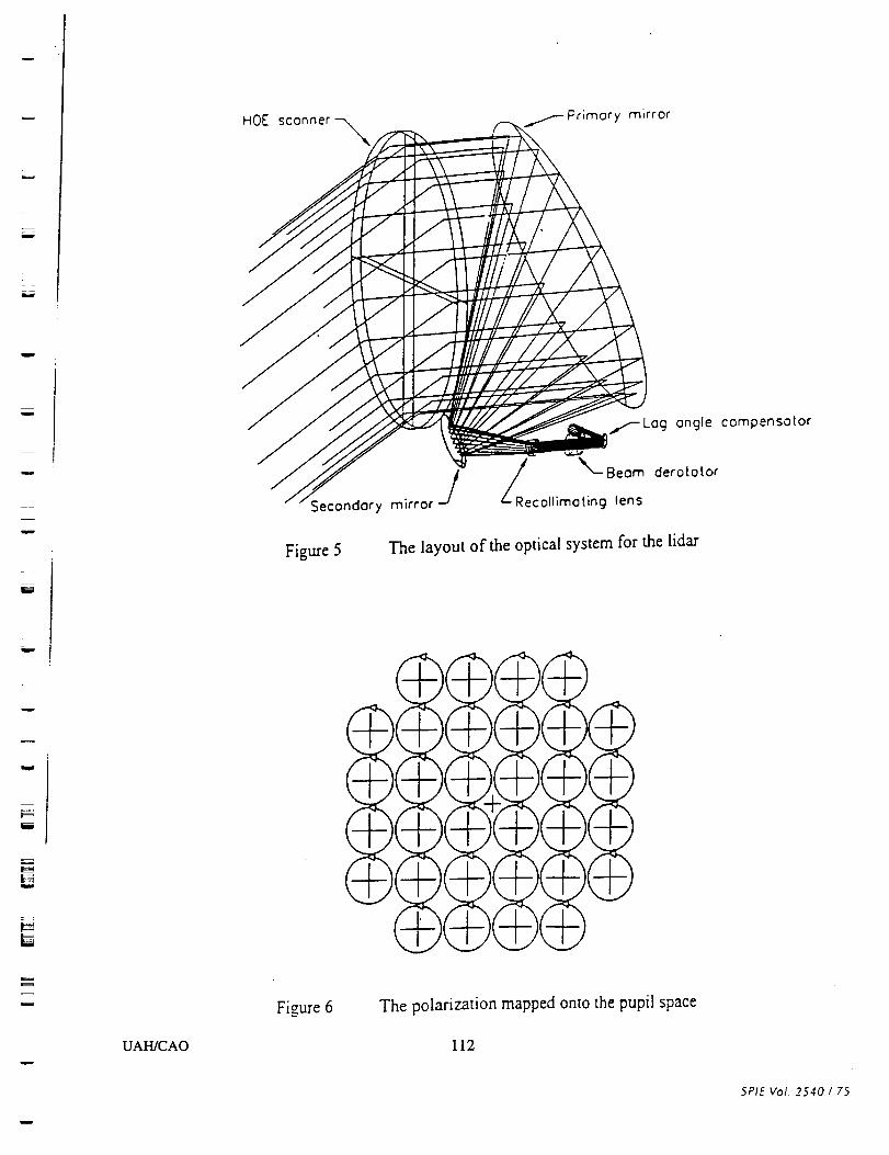
iii
w
_ I
w
oi Figure 5
Primory mirror
,l,--Log ongle
_Re _k_"Beom derotolor
collimoting lens
The layout of the optical system for the lidar
¢ompensotor
UAH/CAO
Figure 6 The polarization mapped onto the pupil space
112
5PIE Vol 2540 / 75
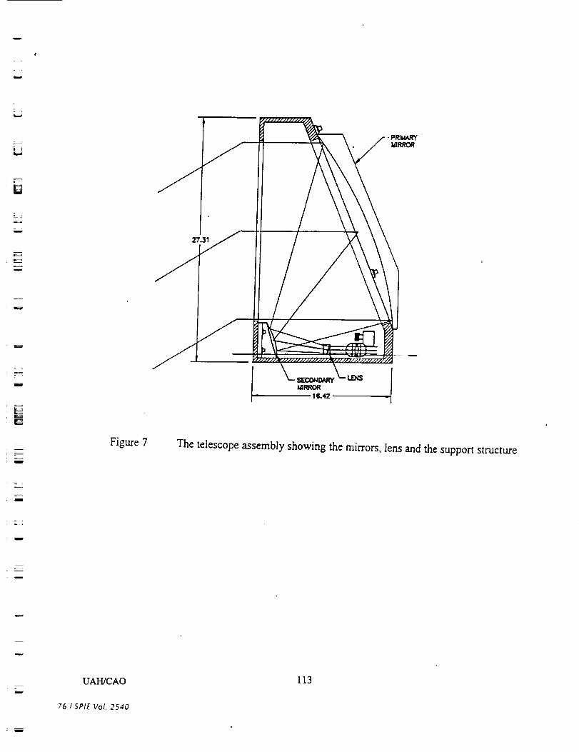
w
m
w
_=w
w
Figure 7The telescope assembly showing _e mirrors, lens and the support structure
w
i
m
f
mw
UA_CAO
76 /5PIE Vol. 2540
113
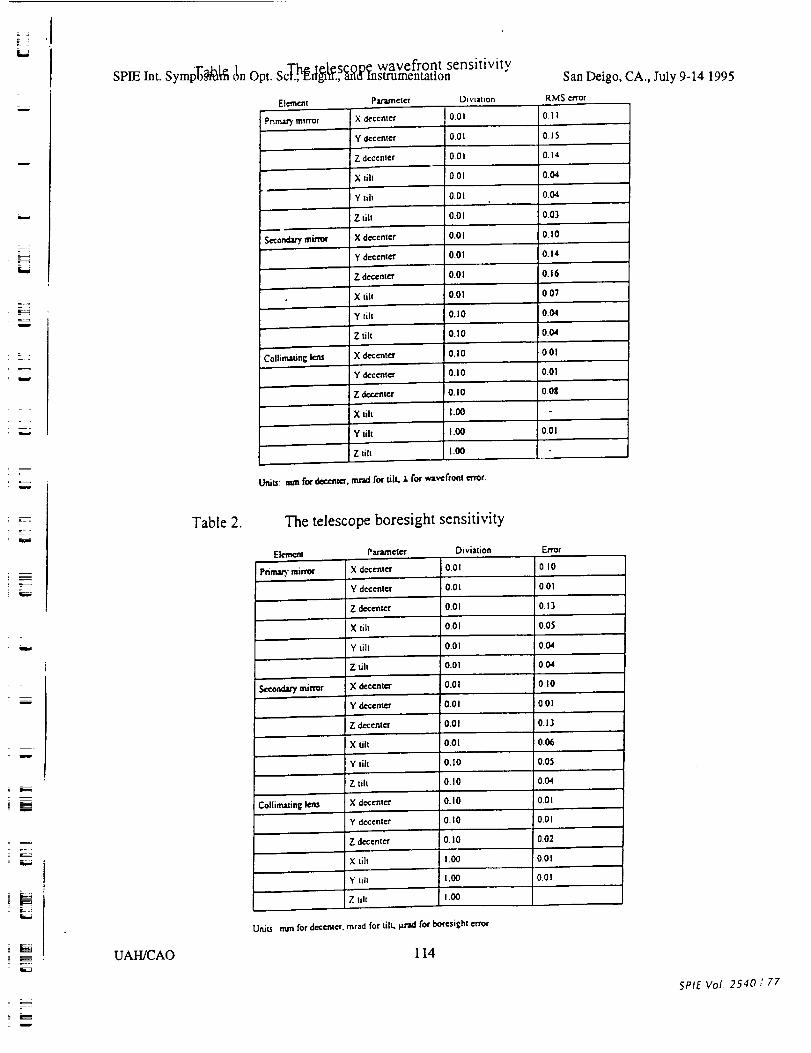
/
,
ScT..h_IelescoDe wavefront sensitMtySPIE Int. Symp]_li_i _n Opt. ., ngm-., ano Instrumentation
Elcmcnt parameter Dwtzuon
Pn m,w/minor
S_ on<i.1_'ymirrori,,,
[_ deccnteTd¢centcr
Z deccnler
X till
Y tih
Z till
X deccnter
San Deigo, CA., Iuly 9-14 1995
RMS cwor
0.11
0.15
0.14
0.04
0.04
0.03
:0.10
Y deccnter O.14
Z deccnt_ O.16
X tilt 0.0"/
Y tilt
Z tilt
X dt-t enter
! Y d¢ccnter
Z _centcr
X tilt
Y tih
0.01
0,01
!o,oi
0.01
0.01
O.OI
0,01
0.01
0.01
0.01
0,I0
O.lO
0.Io
0.10
0.I0
1.00
1.00
1.00
' Collimdng Ic.ns
0.04
0.04
!ool
0.01
0.05
Z tilt
001
Uniu: mm fee dcc._lcr, m_d for tilt, s for wavcfront ¢m>¢.
UAH/CAO
TabLe 2. The telescope boresight sensitivity
Elemcm Parameter Di viation Error
Pnn_." minor X dcccnter
Secondarymirror
Collimating Ic'ns
Y dcccmcr
7. decentcr
X lilt
0,01
0.01
0.01
0.01
Y tilt 0.01
Z tih 0.01
X dcccnto" 0.01
Y dcccntcr
Z dc<:cntcr
X tilt
Y tilt
Z lilt
X dcccntcr
y dcccntcr
Z deccnl_
0.01
'0.01
0.01
0.10
0.10
010
0.01
0.13
0.05
004
0.04
0,10
:0.01
0.13
0.06
0.0_
0.04
0.10 0.01
0,10 O.Ol
O.I0 OO2
X tilt 1.00
Y tilt 1.00
Z ttlt 1.00
Units ram for decentcr, mrad for tilt. t.tradfor borcsight error
0.01
0.01
114
l J,
5PIE Vol 2540 / 77
w
= =w
= =
w
w
i
Coherent Laser Radar Conference Keystone, Colorado, July 23-27, 1995
Characterization of Semiconductor Detectors
For Operation in 2-micron Coherent Lidars
Farzin Amzajerdian
The University Of Alabama in Huntsville
Center for Applied Optics
Huntsville, Alabama 35899
(205) 895-6030 Ext. 452
Brian F. Jones and Michael J. Kavaya
NASA Marshall Space Flight Center
Electro-Optical Branch
MSFC, Alabama 35812
Abstract
The heterodyne detection characteristics of room-temperature semiconductor detectors operating
at 2-micron wavelength region have been investigated. A detector characterization system has
been designed and developed to quantify the performance of these detection devices and to
provide their optimum operating parameters in a coherent lidar system.
Summary
m
w
Most earlier work on optical heterodyne receivers has concentrated on detection devices operating1-4
in the 10-micron region . In view of the growing interest in eye-safe, solid state coherent laser
radars using Thulium and Holmium based lasers, we have investigated the heterodyne detection
characteristics of room-temperature semiconductor detectors operating in the 2-micron
wavelength region. A detector characterization system has been designed and developed atNASA/MSFC that enables the accurate characterization of 2-micron detection devices for
evaluating their performance as heterodyne detectors and determining their optimum operating
parameters. The measured quantities will provide all the necessary detector parameters for
specifying the optimum optical local oscillator power incident on the detector, the detector
optimum bias voltage, and the parameters of the detector interface electronics. The detector
characterization system is also capable of direct measurement of the detector heterodyne quantum
efficiency T_HQE as a function of the IF signal frequency. In a coherent lidar, the signal-to-noise
ratio is directly proportional to the detector heterodyne quantum efficiency, therefore knowledge
of the detector heterodyne quantum efficiency is necessary for initial calibration of coherent lidars
and predicting their performance.
The detector characterization set-up and measurement technique are illustrated in figures 1 and 2.
The measurement system uses two diode-pumped, single mode, continuous wave, Tm, Ho:YLF
(Thulium, Holmium:YLF) lasers developed by Coherent Technologies, Inc. Both lasers can be
UAH/CAO 115
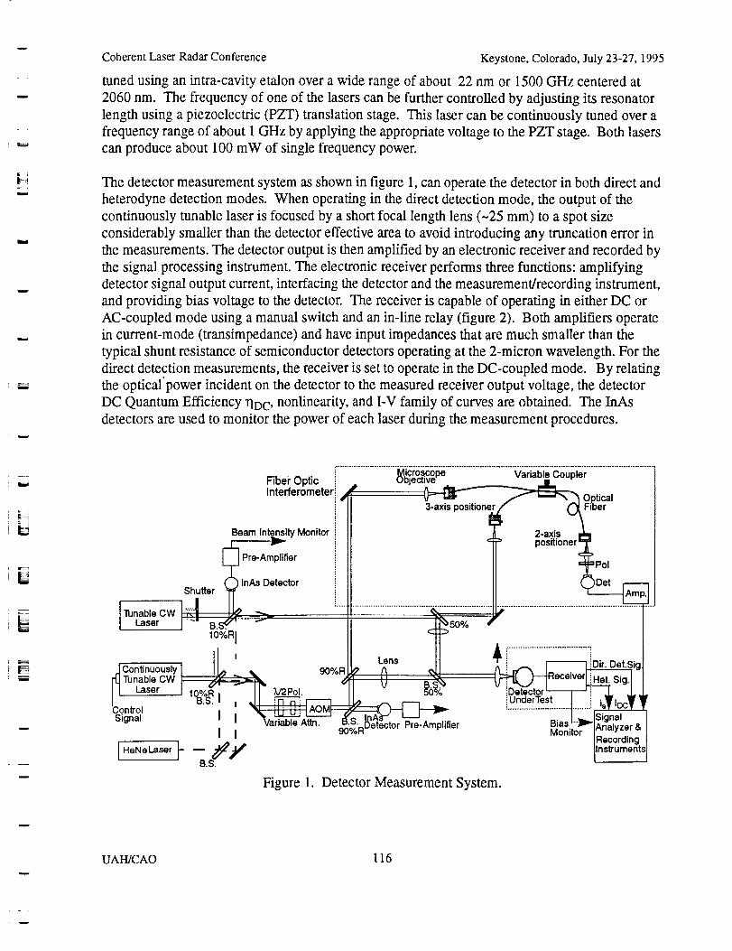
i
L
E
w
w
_ +
Coherent Laser Radar Conference Keystone, Colorado, July 23-27, 1995
tuned using an intra-cavity etalon over a wide range of about 22 nm or 1500 GHz centered at
2060 nm. The frequency of one of the lasers can be further controlled by adjusting its resonator
length using a piezoelectric (PZT) translation stage. This laser can be continuously tuned over a
frequency range of about 1 GHz by applying the appropriate voltage to the PZT stage. Both lasers
can produce about 100 mW of single frequency power.
The detector measurement system as shown in figure 1, can operate the detector in both direct and
heterodyne detection modes. When operating in the direct detection mode, the output of the
continuously tunable laser is focused by a short focal length lens (-25 mm) to a spot size
considerably smaller than the detector effective area to avoid introducing any truncation error in
the measurements. The detector output is then amplified by an electronic receiver and recorded by
the signal processing instrument. The electronic receiver performs three functions: amplifying
detector signal output current, interfacing the detector and the measurement/recording instrument,
and providing bias voltage to the detector. The receiver is capable of operating in either DC or
AC-coupled mode using a manual switch and an in-line relay (figure 2). Both amplifiers operate
in current-mode (transimpedance) and have input impedances that are much smaller than the
typical shunt resistance of semiconductor detectors operating at the 2-micron wavelength. For the
direct detection measurements, the receiver is set to operate in the DC-coupled mode. By relating
the optical'power incident on the detector to the measured receiver output voltage, the detector
DC Quantum Efficiency rid C, nonlinearity, and I-V family of curves are obtained. The InAs
detectors are used to monitor the power of each laser during the measurement procedures.
U
W
w
Shutter
Tunable CW
Laser
Fiber OpticInterferometer
Beam Inte=nnsityMonitor
ro-Am er
InAs Detector
J_,icro.scope Variable CoupleruDjectlve
# Optical3-axis F_er
2-axispositioner'
10%R I
I Lens +
C°ntinu°uslyTunable CW
ntrolSignal I I
I I
[ HeNeLaser ]- --_. S<_/
90%R
L/2Pol.
, Attn. Pre-Amplifier
ilunderTest
BiasMonitor
Signal&
Recording
Figure 1. Detector Measurement System.
UAH/CAO 116
w
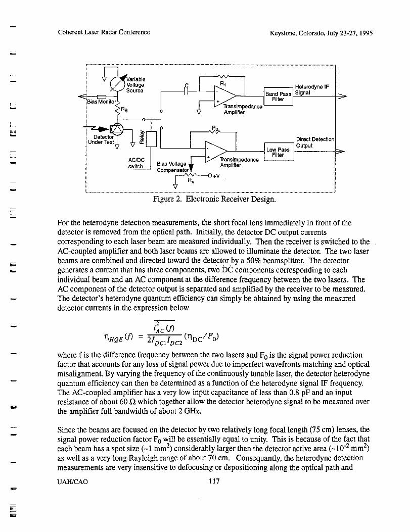
wCoherent Laser Radar Conference Keystone, Colorado, Iuly 23-27, 1995
w
/
w
m
U
_¢Variable
_,/ ) Voltaget, _ Source
Bias Monito_
RB o-
Det
Uodar st
switch Compensator_
-'-__pe I Heterodyne IF
Band Pass Signal
dance Filter
Direct Detection
I Low Pass I OutputNiter
Figure 2. Electronic Receiver Design.
f
f
For the heterodyne detection measurements, the short focal lens immediately in front of the
detector is removed from the optical path. Initially, the detector DC output currents
corresponding to each laser beam are measured individually. Then the receiver is switched to the
AC-coupled amplifier and both laser beams are allowed to illuminate the detector. The two laser
beams are combined and directed toward the detector by a 50% beamsplitter. The detector
generates a current that has three components, two DC components corresponding to each
individual beam and an AC component at the difference frequency between the two lasers. The
AC component of the detector output is separated and amplified by the receiver to be measured.
The detector's heterodyne quantum efficiency can simply be obtained by using the measured
detector currents in the expression below
.2t A C (f)
I"IHQE (j9 - 2IDcIIDc 2 (1"IDc/F O)
where f is the difference frequency between the two lasers and F 0 is the signal power reduction
factor that accounts for any loss of signal power due to imperfect wavefronts matching and optical
misalignment. By varying the frequency of the continuously tunable laser, the detector heterodyne
quantum efficiency can then be determined as a function of the heterodyne signal IF frequency.
The AC-coupled amplifier has a very low input capacitance of less than 0.8 pF and an input
resistance of about 60 f_ which together allow the detector heterodyne signal to be measured over
the amplifier full bandwidth of about 2 GHz.
Since the beams are focused on the detector by two relatively long focal length (75 cm) lenses, the
signal power reduction factor F 0 will be essentially equal to unity. This is because of the fact thateach beam has a spot size (-1 mm 2) considerably larger than the detector active area (-10 -2 mm 2)
as well as a very long Rayleigh range of about 70 cm. Consequantly, the heterodyne detection
measurements are very insensitive to defocusing or depositioning along the optical path and
UAH/CAO 117
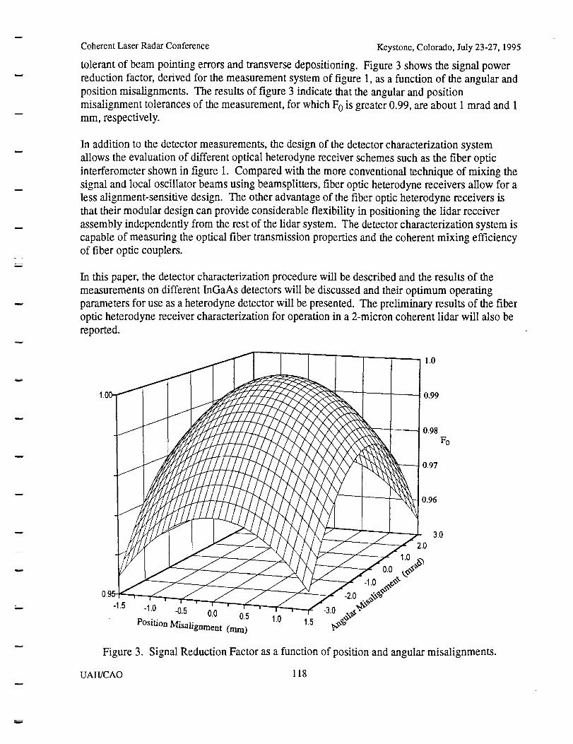
r_w
w
w
w
Coherent Laser Radar Conference Keystone, Colorado, July 23-27, 1995
tolerant of beam pointing errors and transverse depositioning. Figure 3 shows the signal power
reduction factor, derived for the measurement system of figure 1, as a function of the angular and
position misalignments. The results of figure 3 indicate that the angular and position
misalignment tolerances of the measurement, for which Fo is greater 0.99, are about 1 mrad and 1
ram, respectively.
In addition to the detector measurements, the design of the detector characterization system
allows the evaluation of different optical heterodyne receiver schemes such as the fiber optic
interferometer shown in figure 1. Compared with the more conventional technique of mixing the
signal and local oscillator beams using beamsplitters, fiber optic heterodyne receivers allow for a
less alignment-sensitive design. The other advantage of the fiber optic heterodyne receivers is
that their modular design can provide considerable flexibility in positioning the lidar receiver
assembly independently from the rest of the lidar system. The detector characterization system is
capable of measuring the optical fiber transmission properties and the coherent mixing efficiency
of fiber optic couplers.
In this paper, the detector characterization procedure will be described and the results of the
measurements on different InGaAs detectors will be discussed and their optimum operating
parameters for use as a heterodyne detector will be presented. The preliminary results of the fiber
optic heterodyne receiver characterization for operation in a 2-micron coherent lidar will also be
reported.
1.00-
-1.0 -0.5 0.0 0.5
Position Misaligament (ram)
0.99
0.98
Fo
Figure 3. Signal Reduction Factor as a function of position and angular misalignments.
UAH/CAO 118
w
m
Coherent Laser Radar Conference Keystone, Colorado, July 23-27, 1995
w
L_
w
w
References
1. T. G. Blaney, "Signal-to-noise ratio and other characteristics of heterodyne radiation
receivers," Space Science Reviews 17, 1975
2. D. L. Spears, "Long-wavelength photodiode development," NASA report no. NAS-5-25717,
August 1983
3. J. M. Hunt, J. E Holmes, and F. Amzajerdian, "Optimum local oscillator levels for coherent
detection using photoconductors," Appl. Opt. 27, August 1988
4. J. E Holmes and B. J. Rask, "Optimum optical local-oscillator power levels for coherent
detection with photodiodes," Appl. Opt. 34, February 1995
m
w
UAH/CAO 119
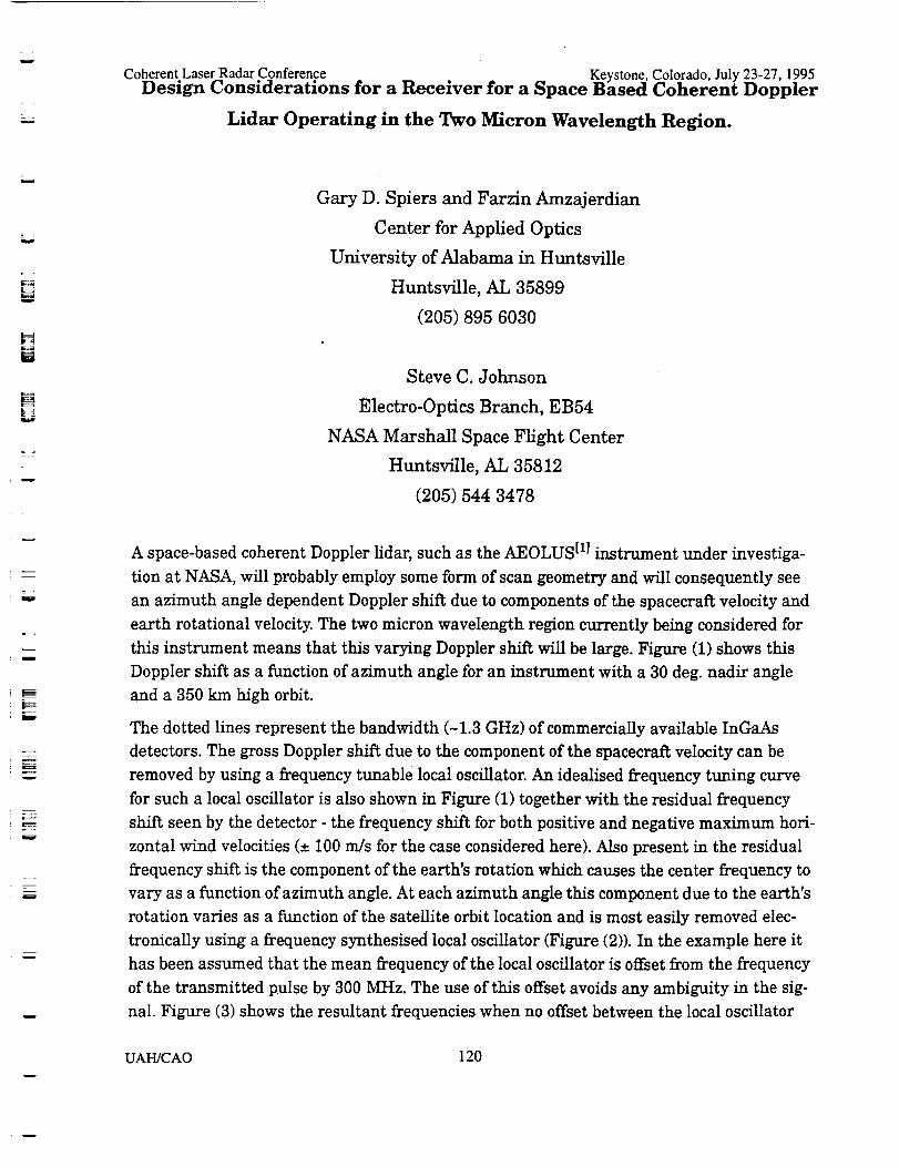
w
w
i
L
m
L_
w
Coherent Laser Radar Conference Keystone, Colorado, July 23-27, 1995Design Considerations for a Receiver for a Space Based Coherent Doppler
Lidar Operating in the Two Micron Wavelength Region.
Gary D. Spiers and Farzin Amzajerdian
Center for Applied Optics
University of Alabama in Huntsville
Huntsville, AL 35899
(205) 895 6030
Steve C. Johnson
Electro-Optics Branch, EB54
NASA Marshall Space Flight Center
Huntsville, AL 35812
(205) 544 3478
--==
--=
w
A space-based coherent Doppler lidar, such as the AEOLUS [i] instrument under investiga-
tion at NASA, will probably employ some form of scan geometry and will consequently see
an azimuth angle dependent Doppler shift due to components of the spacecraft velocity and
earth rotational velocity. The two micron wavelength region currently being considered for
this instrument means that this varying Doppler shift will be large. Figure (1) shows this
Doppler shift as a function of azimuth angle for an instrument with a 30 deg. nadir angle
and a 350 km high orbit.
The dotted lines represent the bandwidth (-1.3 GHz) of commercially available InGaAs
detectors. The gross Doppler shift due to the component of the spacecraft velocity can be
removed by using a frequency tunable local oscillator. An idealised frequency tuning curve
for such a local oscillator is also shown in Figure (1) together with the residual frequency
shift seen by the detector - the frequency shift for both positive and negative maximum hori-
zontal wind velocities (± 100 m/s for the case considered here). Also present in the residual
frequency shift is the component of the earth's rotation which causes the center frequency to
vary as a function of azimuth angle. At each azimuth angle this component due to the earth's
rotation varies as a function of the satellite orbit location and is most easily removed elec-
tronically using a frequency synthesised local oscillator (Figure (2)). In the example here it
has been assumed that the mean frequency of the local oscillator is offset from the frequency
of the transmitted pulse by 300 MHz. The use of this offset avoids any ambiguity in the sig-
nal. Figure (3) shows the resultant frequencies when no offset between the local oscillator
UAH/CAO 120
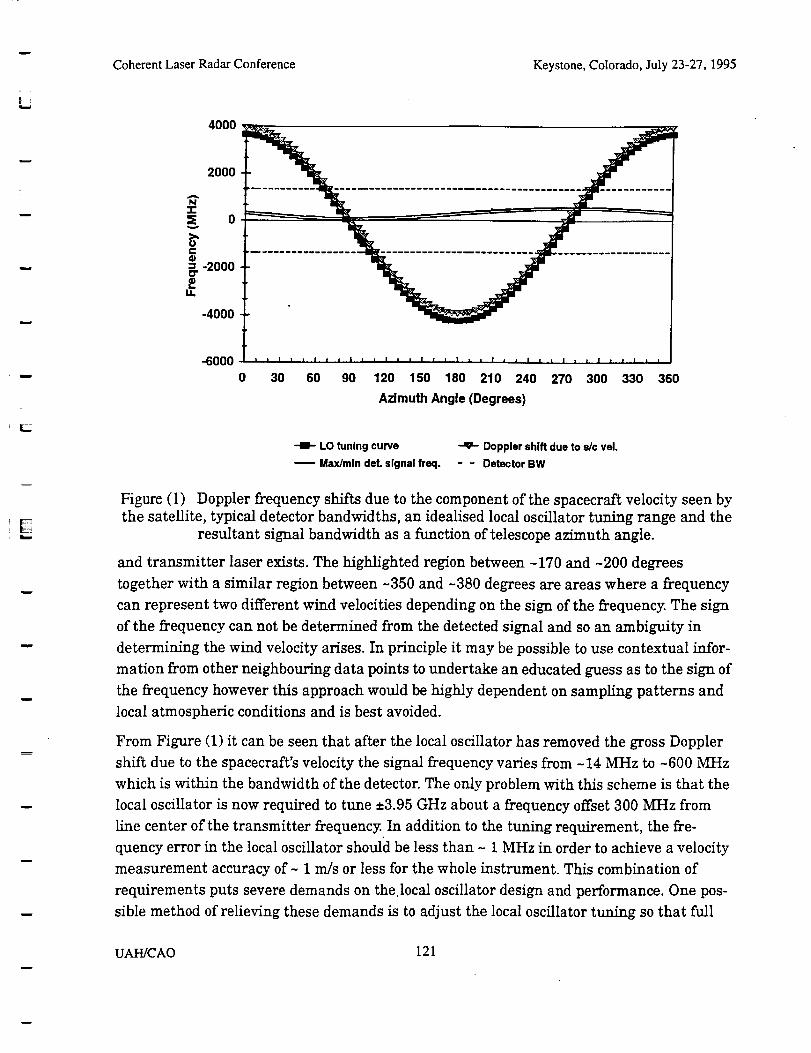
w
Coherent Laser Radar Conference Keystone, Colorado, July 23-27, 1995
4000
w
2000
0
o>,e-¢D= -20000"G
-4000
L
.-6OO0
0 30 60 90 120 150 180 210 240 270 300 330 360
A_muth Angle(Degrees)
LO tuning curve _ Doppler shift due to s/¢ vel.
Max/mln det. signal freq. - - Detector BW
Figure (1) Doppler frequency shifts due to the component of the spacecraft velocity seen by
the satellite, typical detector bandwidths, an idealised local oscillator tuning range and the
resultant signal bandwidth as a function of telescope azimuth angle.
and transmitter laser exists. The highlighted region between -170 and -200 degrees
together with a similar region between -350 and -380 degrees are areas where a frequency
can represent two different wind velocities depending on the sign of the frequency. The sign
of the frequency can not be determined from the detected signal and so an ambiguity in
determining the wind velocity arises. In principle it may be possible to use contextual infor-
mation from other neighbouring data points to undertake an educated guess as to the sign of
the frequency however this approach would be highly dependent on sampling patterns and
local atmospheric conditions and is best avoided.
From Figure (1) it can be seen that after the local oscillator has removed the gross Doppler
shift due to the spacecraft's velocity the signal frequency varies from -14 MHz to -600 MHz
which is within the bandwidth of the detector. The only problem with this scheme is that the
local oscillator is now required to tune +3.95 GHz about a frequency offset 300 MHz from
line center of the transmitter frequency. In addition to the tuning requirement, the fre-
quency error in the local oscillator should be less than ~ 1 MHz in order to achieve a velocity
measurement accuracy of- 1 m/s or less for the whole instrument. This combination of
requirements puts severe demands on the local oscillator design and performance. One pos-
sible method of relieving these demands is to adjust the local oscillator tuning so that full
UAH/CAO 121
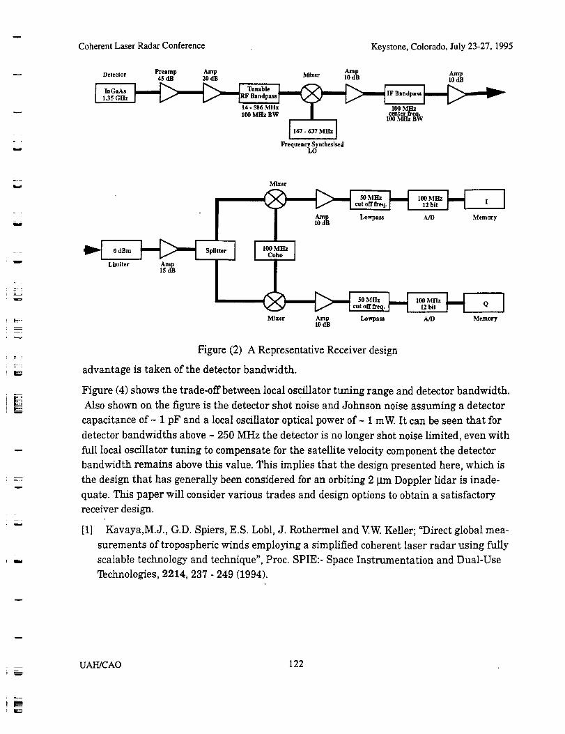
w
Coherent Laser Radar Conference Keystone, Colorado, July 23-27, I995
Detector Preamp Amp Mixer Amp45 dB 20 dB [0 dB
1_5 GHz _RF Bandpau IF Bandpass
14 - 586 MHz I I00 MHz100 Mltz BW I .een.ter__e_.q._.
I I00 MItz BW
I 167- 637 MHz I
Frequency SynthesisedLO
Amp1o dB
L=
F
w
w
m
0dBm _ Splitter [
Limiter lsAmd_
Mixer
5OMHz
cut off l_'eq.
Am Lowpa_
100 MHz ICoho
100 MHz [12bit I
A/D Memory
_lm_ 50 MHz 100 MHz
cut offfi'eq. H 12bit _mmm_
Mixer Amp Lowpa_ A/D10 dB
Q
Memory
Figure (2) A Representative Receiver design
advantage is taken of the detector bandwidth.
Figure (4) shows the trade-off between local oscillator tuning range and detector bandwidth.
Also shown on the figure is the detector shot noise and Johnson noise assuming a detector
capacitance of ~ 1 pF and a local oscillator optical power of - 1 mW. It can be seen that for
detector bandwidths above - 250 MHz the detector is no longer shot noise limited, even with
full local oscillator tuning to compensate for the satellite velocity component the detector
bandwidth remains above this value. This implies that the design presented here, which is
the design that has generally been considered for an orbiting 2 laxn Doppler lidar is inade-
quate. This paper will consider various trades and design options to obtain a satisfactory
receiver design.
[1] Kavaya,M.J., G.D. Spiers, E.S. Lobl, J. Rothermel and V.W. Keller; "Direct global mea-
surements of tropospheric winds employing a simplified coherent laser radar using fully
scalable technology and technique", Prec. SPIE:- Space Instrumentation and Dual-Use
Technologies, 2214, 237 - 249 (1994).
UAH/CAO 122
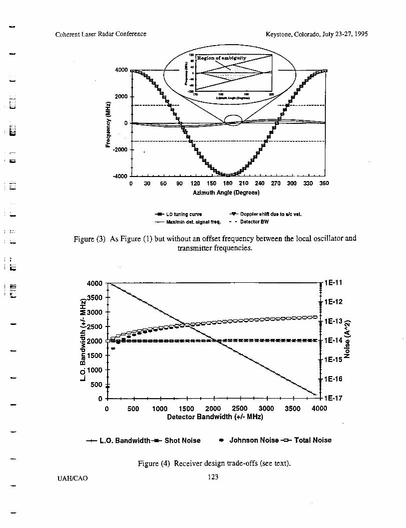
r--W
L
P-,z=ff
Coherent Laser Radar Conference Keystone, Colorado, July 23-27, 1995
4OOO
20OO
i °-2000
-4O000 30 60 90 120 150 180 210 240 270 300 330 360
Azlmuth Angle (Degrees)
Figure (3)
-_- LO tuning curve -q=- Doppler shift due to s/c vel.
Max/mln det. signal freq. - - Detector BW
As Figure (1) but without an offset frequency between the local oscillator and
transmitter frequencies.
4000
,-.3500N
3000!
+2500
_2000
c1500
o1000
500
_-1E-11
1E16
0 500 1000 1500 2000 2500 3000 3500
Detector Bandwidth (+h MHz)
1E-17
4000
-+- L.O. Bandwidth--=- Shot Noise e Johnson Noise-m- Total Noise
UAH/CAO
Figure (4) Receiver design trade-offs (see text).
123
w
w
REFERENCES
1. D.L. Spears and R.H. Kingston, "Anomalous noise behavior in wide-bandwidth photodiodes
in heterodyne and background-limited operation," Appl. Phys. Lett. 34, May 1979.
2. R.G. Frehlich and M. J. Kavaya, "Coherent laser radar performance for general atmospheric
refractive turbulence," Appl. 30, December 1991
3. R.T. Ku and D.L. Spears, "High-sensitivity infrared heterodyne radiometer using a tunable-
diode-laser local oscillator," Opt. Lett. 1, September 1977.
4. R.G. Frehlich, "Estimation of the nonlinearity of a photodetector," Appl. Opt. 31, October
1992.
5. J.F. Holmes and B. J. Rask, "Optimum optical local-oscillator power levels for coherent
detection with photodiodes," Appl. Opt. 34, February 1995
6. J.M. Hunt, J. F. Holmes, and E amzajerdian, "Optimum local oscillator levels for coherent
detection using photoconductors," AppI. Opt. 27, August 1988
7. Farzin Amzajerdian, "Analysis of measurements for solid state laser remote lidar system,"
Final Report, Contract No. NAS8-38609/D.O. 77, September 31, 1994
8. M.J. Post and R.E. Cupp, "Optimizing a pulsed Doppler lidar," Appl. Opt. 29, October 1990.
9. H. van de Stadt, "Heterodyne detection at a wavelength of 3.39 p.m for astronomical
purposes," Astron. and Astrophys. 36, 341-348, 1974.
10. J. J. Morikuni, A. Dharchoudhury, Y. Leblebici, and S. M. Kang, "Improvements to the
standard theory for photoreceiver noise," IEEE J. Lightwave Technol., v. 12, July 1994.
11. B. L. Kasper and J. C. Campbell, "Multigigabit-per-second avalanche photodiode lightwave
receivers," IEEE J. Lightwave Technol., v. 5, October 1987.
12. R. A. Minasian, "Optimum Design of a4-Gbit/s GaAs MESFET optical preamplifier,"
IEEE J. Lightwave Technol., v. 5, March 1987.
13. "Definition and Preliminary Design of the LAWS (Laser Atmospheric Wind Sounder)
Phase II Final Report Volume II," NASA Contract No. NAS8-37589,
GE Astro Space Division, September 1992.
14. "Design Definition of the Laser Atmospheric Wind Sounder (LAWS)", Lockheed Missiles &
Space Company, Huntsville, AL, Phase II Final Report, Contract No. NAS8-37590,
November 1992. Pages from 3-60 to 3-70.
UAH/CAO 124
w
w
= r
I
15.
16.
17.
18.
19.
20.
21.
22.
J. Bilbro, G. Fichtl, D. Fitzjarrald, M. Krause, and R. Lee, "Airborne Doppler lidar wind field
measurements", Am. Met. Soc. 65, April 1984.
M.J. Kavaya, G.D. Spiers, E.S. Lobl, J'. Rothermel, and V.W. Keller, "Direct global
measurements of tropospheric winds employing a simplified coherent laser radar using fully
scalable technology and technique," Proc. Of SPIE International Symposium on Optical
Engineering in Aerospace Sensing, Technical Conference on Space Instrumentation and Dual-
Use Technologies, 2214-31, Apr 6, 1994.
J.G. Hawley, R. Targ, S.W. Henderson, C.R Hale, M.J. Kavaya, and D. Moerder, "Coherent
launch-site atmospheric wind sounder: theory and experiment" Appl. Opt. 32, August 1993.
R.T. Menzies, "Doppler lidar atmospheric wind sensor: a comparative performance
evaluations for global measurement applications from earth orbit," Appl. Opt. 25,
August 1986.
W.E. Baker, G.D. Emmitt, R Robertson, R.M. Atlas, J.E. Molinari, D.A. Bowdle, J. Paegle,
R.M. Hardesty, R.T. Menzies, T.N. Krishnamurti, R.A. Brown, M.J. Post, J.R. Anderson,
A. C. Lorenc, T.L. Miller, and J. McElroy, "Lidar measured winds from space: An essential
component for weather and climate prediction," To be published in the Bulletin of American
Meteorological Society, 1995.
L. Kristensen and D.H. Lenschow, "The spectral velocity tensor for homogeneous
boundary-layer turbulence," Boundary-Layer Meteorology 47, 149-193, Kluwer Academic
Publishers, Netherlands, 1989.
L. Kristensen and J.E. Gaynor, "Errors in second moments estimated from monostatic
Doppler sodar winds. Part I: Theoretical Description," J. Atm and Oceanic Tech. 3,
September 1986.
L. Kristensen and D.H. Lenschow, "An airborne laser air motion sensing system, Part II:
Design criteria and measurement possibilities," J. Atm and Oceanic Tech. 4, 1987.
ii -_:_
m
L
UAH/CAO 125

w
_=
1 im_!f
_A_A
• Heport No. -' L_ovemmem AC_10n NO.Report Document
;3.Hec=p_r_'s ¢.;_ax_ No. ' ....
for Solid State
¢._tl_ and Subtile
Analysis of Measurements
Lidar Development
7. Author(s)
Farzln Amzajerdian
]. Pedormmg OrganizaZlon Name and Address
University of ALabama in Huntsville, _Huntsville, Alabama 35899
2. Sponsoring Agency Name and Address
National Aeronautics and Space AdministrationWashington, D.C. 20546--001
Marshall Space FraghtCenter, AL 35812
15. Supplementa/y Notes
5. Report Due
December 1995
,=,. ,,
5. Perforrr=ng Organization Code
University of Alabama in Huntsville
9. Performing Organization Report No.
0. Work Unit No.
1. Contract or Grant No.
NAS8-38609 "]_.O. I{
13. Type of report and Period covered
Final - 8/8/94 - 12/7/95
14. Sponsonng Agency Code
16.Abstrac_
17. Key Words (Suggested by Author(s))
9. Security Class. (o| this repor:t)
18. Distribution Stmement
20. ,S_urtty Class. (of this page) 21. No. of pages
Unclassified Unclassified
NASA FORM 1626 OCT 86
22. Price