analysis and prototyping of multicellular dc-dc ... · system is the effective utilization of the...
TRANSCRIPT

Journal of Energy and Power Engineering 10 (2016) 313-323 doi: 10.17265/1934-8975/2016.05.006
Analysis and Prototyping of Multicellular DC-DC
Transformer for Environmentally Friendly Data Centers
Yusuke Hayashi and Tamotsu Ninomiya
Power Electronics Circuits and Systems Laboratory, Green Electronics Research Institute, Kitakyushu, Fukuoka 808-0135, Japan
Received: March 02, 2016 / Accepted: March 15, 2016 / Published: May 31, 2016. Abstract: A multicellular DCX (dc-dc transformer) using unregulated cell converters has been proposed for the environmentally friendly data centers. The high speed cell converter with the switching frequency over MHz behaves as an ideal transformer, and this behavior solves the voltage imbalance issue in the multicellular converter topology. The analysis of the unregulated cell converter is conducted by using the state space averaging method, and the operation condition for the ideal transformer is specified. The behavior of the multicellular DCX using the high speed cell converters has been also analyzed, and the voltage imbalance issue among cell converters is discussed quantitatively. A prototype of a 19.2 kW 384 V-384 V multicellular DCX using sixty-four unregulated cell converters is fabricated and the validity of the analyses is verified.
Key words: DCX (dc-dc transformer), high frequency dc-dc converter, ISOP (input series output parallel), IPOS (input parallel output series), state space averaging method.
1. Introduction
The amount of network traffic in the data centers has
recently been rapidly increasing due to the widespread
use of ICT (information and communication
technology) equipment [1, 2]. Energy conservation and
resource saving in data centers will contribute to
solving some of our global environmental problems.
NTT (Nippon Telegraph and Telephone) Group has
been proposing a next generation dc (direct current)
distribution system, that goes beyond the conventional
380 V dc distribution system to realize the highly
electrified low carbon society [3-5].
One of features of the proposed dc distribution
system is the effective utilization of the renewable
energy sources. The highly efficient and the highly
scalable DCX (dc-dc transformer) is the only
component to interface various voltage levels of the
energy storage devices and the renewable energy
sources flexibly. The multicellular converter topology
Corresponding author: Yusuke Hayashi, Ph.D., research
fields: dc distribution system, dc power supply and power electronics system integration.
based on the ISOP (input series output parallel) IPOS
(input parallel output series) connection of low
voltage low power cell converters is one of options to
realize the high scalable DCX.
In this paper, the multicellular DCX using
unregulated cell converters is proposed. The cell
converter with no voltage regulation is applied to the
DCX because the functions of the transformer are the
voltage transformation and the isolation. The
multicellular dc-dc converters with the regulated cell
converters have been already proposed and their
control stabilities have been also reported [6-10].
However, the stability issue such as the voltage
imbalance among cell converters has not been
discussed quantitatively in case that, the unregulated
dc-dc converter is applied to the cell converter.
In Section 2, the concept of the DCX based on the
multicellular converter topology is introduced. In
Section 3, the behavior of the unregulated single cell
converter is analyzed by using the state space
averaging method, and the operating condition of the
cell converter is specified to develop the multicellular
D DAVID PUBLISHING

Analysis and Prototyping of Multicellular DC-DC Transformer for Environmentally Friendly Data Centers
314
DCX. In Section 4, the static and the dynamic
behaviors of the ISOP connected multicellular DCX
are analyzed, and the voltage imbalance issue among
the cell converters is discussed quantitatively. The
validity of the aforementioned analyses is verified by
fabricating a prototype of a 384 V-384 V 19.2 kW
multicellular DCX composed of sixty-four dc-dc cell
converters with the I/O (input and output) voltages of
48 V-48 V and the output power of 300 W.
2. DC-DC Transformer Based on Multicellular Converter Topology in Next Generation DC Distribution System
2.1 Configuration of Next Generation DC Distribution System for Environmentally Friendly Data Centers
The schematic illustration of the next generation dc
distribution system is shown in Fig. 1. The main
power distribution system consists of the following
power electronics equipment:
The front end ac-dc converter;
The DCX;
The POL (point of load) dc-dc converter.
The front end ac-dc converter is utilized for the
interface with the ac grid and for the control of the
output dc voltage. The DCX is installed for the
isolation and the voltage transformation, and the
function of the voltage regulation is not necessary.
Equipment with various I/O voltage levels are
connected via the DCX. The POL converter is
installed to regulate the load voltage strictly.
In the next generation dc distribution system, the
energy storages and the distributed generators based
on the renewable energy sources will be installed in
addition to the ICT equipment, such as the servers and
the storages to realize the environmentally friendly
power supply system. The input and the output
voltage levels of these applications are e.g., 384 V,
192 V, 48 V and 12 V, and they have different
grounding systems. The DCX for the isolation and the
voltage transformation plays an important role in this
system, and the high scalability of the DCX
contributes to the smooth installation of a lot of
renewable power sources and energy storage devices.
2.1 DC-DC Transformer Based on Multicellular
Converter Topology
The multicellular converter topology is one of
attractive options to discuss the feasibility of the
highly efficient DCXs with various I/O voltage levels
such as 384 V-12 V, 384 V-48 V and 384 V-384 V.
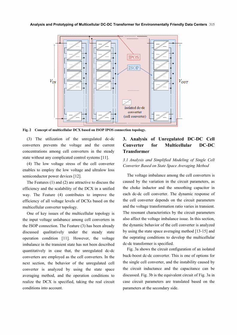
The concept of the multicellular DCX is shown in
Fig. 2. The DCX consists of a lot of isolated dc-dc cell
converters, and these cell converters are connected in
types of ISOP and IPOS. The unregulated power
converters are utilized as the cell converters because
the DCXs are installed for the isolation and the
voltage transformation. The features of the DCX are
summarized as follows:
(1) The efficiency η (%) and the power density
Dp (W/cm3) of the DCX is decided by the single cell
converter.
(2) The I/O voltages of the DCX are designed
arbitrarily by the number of cell converters connected
in series and parallel.
Fig. 1 Configuration of next generation dc distribution system for environmentally friendly data centers.
Analysi
Fig. 2 Conc
(3) The
converters
concentratio
state withou
(4) The l
enables to e
semiconduct
The Featu
efficiency an
way. The F
efficiency o
multicellular
One of k
the input vo
the ISOP co
discussed
operation c
imbalance in
quantitativel
converters a
next section
converter i
averaging m
realize the D
conditions in
s and Prototy
ept of multicel
utilization
prevents the
ons among c
ut any complic
low voltage
employ the lo
tor power dev
ures (1) and (
nd the scalab
Feature (4)
f all voltage
r converter to
ey issues of
oltage unlaba
nnection. The
qualitatively
condition [1
n the transien
ly in case
are employed
n, the behav
s analyzed
method, and
DCX is spec
nto account.
yping of Mult
llular DCX bas
of the un
e voltage a
cell converter
cated control
stress of th
ow voltage a
vices [12].
2) are attracti
bility of the D
contributes
levels of DC
opology.
the multicel
ance among c
e Feature (3)
under the
11]. Howeve
nt state has no
that, the un
d as the cell c
vior of the
by using
the operatio
cified, taking
ticellular DC-
sed on ISOP IP
nregulated d
and the cur
rs in the ste
systems [11]
he cell conve
and ultralow
ive to discuss
DCX in a uni
to improve
CXs based on
lular topolog
cell converter
has been alre
e steady s
er, the vol
ot been descr
nregulated d
converters. In
unregulated
the state sp
on condition
g the real cir
DC Transform
POS connectio
dc-dc
rrent
eady
].
erter
loss
s the
ified
the
n the
gy is
rs in
eady
state
ltage
ribed
dc-dc
n the
cell
pace
ns to
rcuit
3. CoTra
3.1 Con
T
cau
the
each
the
and
The
also
the
by u
the
dc-dF
buc
the
the
disc
case
para
mer for Envir
on topology.
Analysis nverter ansformer
Analysis andnverter Based
The voltage im
used by the v
choke induc
h dc-dc cell
cell convert
d the voltage t
e resonant ch
o affect the vo
dynamic beh
using the stat
oeprating co
dc transformeFig. 3a shows
ck-boost dc-d
single cell co
circuit indu
cussed. Fig. 3
e circuit par
ameters at the
ronmentally F
of Unregufor Mu
d Simplified d on State Spa
mbalance am
variation in t
ctor and the
converter. T
ter depends o
transformatio
haracteristics
oltage imbala
havior of the
te space avera
onditions to
er is specifiedthe circuit co
dc converter.
onverter, and
uctance and
3b is the equiv
rameters are
e secondary s
Friendly Data
ulated DCulticellular
Modeling oface Averaging
mong the cell
the circuit pa
e smoothing
The dynamic
on the circui
on ratio varies
by the circui
ance issue. In
cell converte
aging method
develop the
d. onfiguration o
This is one o
d the instabili
the capacita
valent circuit
translated b
side.
Centers 315
C-DC CellDC-DC
f Single Cellg Method
converters is
arameters, as
capacitor in
response of
it parameters
s in transient.
it parameters
n this section,
er is analyzed
d [13-15] and
multicellular
of an isolated
of options for
ity caused by
ance can be
t of Fig. 3a in
based on the
5
l C
l
s
s
n
f
s
.
s
,
d
d
r
d
r
y
e
n
e

Analysi
316
Fig. 3 Circconverter and
In the cas
behavior of
by using the
dd
The input
converter ar
symbols of
and the out
input voltag
ratio of the c
D’ is cons
assumed her
From Eq
and the ou
through the
Eq. (2) m
Vo(s)/Vi(s)
frequency o
transient sta
described as
s and Prototy
cuit configurad (b) equivalen
e of turn ratio
the dc-dc con
e state space a
0′
t inductor an
re expressed b
iL and vo mea
tput capacito
e is Vi and th
converter is D
stant because
re.
. (1), the rel
utput voltage
Laplace trans
′1
′
√
means that, the
of the cell
of the input
ate. In case
s the exponen
yping of Mult
ation of (a) isnt circuit.
o of the trans
nverter is des
averaging me
′
1
nd the output
by L and C, r
ans the input
or voltage, r
he resistive lo
D (D’ = 1 – D
e the unreg
lationship be
es are calcul
sformation.
1
,1
2 ′
e voltage tran
converter d
t voltage flu
e that, the i
ntial startup fu
ticellular DC-
solated buck-b
sformer n = 1
cribed as foll
thod.
0
t capacitor of
respectively.
t inductor cur
respectively.
ad is R. The d
D). The duty r
gulated DCX
etween the in
lated as foll
nsformation r
depends on
uctuation in
input voltag
functions with
DC Transform
boost
, the
lows
(1)
f the
The
rrent
The
duty
ratio
X is
nput
lows
(2)
ratio
the
the
e is
h the
amp
volt
T
the
inve
sho
a 48
swi
for
circ
the
cap
swi
Fig.freqinpu
Tab
I/O
Ou
Ind
Du
Tur
Tim
Rip
Fre
Ind
Cap
mer for Envir
plitude of uni
tage can be fo
′
The voltage tr
transient con
erse Laplace
ws the calcul
8 V-48 V 30
itching freque
this calculat
cuit paramete
switching rip
acitor voltag
itching freque
. 4 Output quency of 300 ut voltage vari
ble 1 Paramet
O voltages Vi, Vo
tput power
ductor current iL
ty ratio D
rn ratio n
me constant Ti
pple rate α, β
equency fSW
ductance L
pacitance C
ronmentally F
ity and the tim
ormulated by
·1
1
ransformation
ndition can b
e transforma
lation results
00 W buck-bo
ency is varied
tion are sum
ers L and C
pples of the in
e Vo. These p
ency fSW and o
· ∆·
voltages of kHz, 500 kHzation with Ti =
ters for analys
o 48 V, 48 V
300 W
L 6.25 A
0.5
1
50 μs (corr
0.2, 0.03
300 kHz 5
64 μH 3
7.23 μF 4
Friendly Data
me constant T
y Eq. (3).
·1
1
n ratio of the
be discussed
ation of Eq.
s of the outpu
oost converte
d. The detaile
mmarized in T
are designed
nductor curre
parameters d
obtained as fo
·· ·
dc-dc convertz, 1 MHz and = 50 μs.
sis of single cel
V
respond to 10 kH
500 kHz 1 MH
38.4 μH 19.2
4.84 μF 2.17
Centers
Ti, the output
·1
(3)
e converter in
d through the
(3). Fig. 4
ut voltages of
er in case the
ed parameters
Table 1. The
d to suppress
ent IL and the
epend on the
ollows.
(4)
ters with the3 MHz under
l converter.
Hz)
Hz 3 MHz
μH 6.4 μH
μF 0.72 μF
t
n
e
4
f
e
s
e
s
e
e
e r

Analysi
Fig. 4 m
with small L
For examp
switching op
which incre
which corres
Fig. 5 s
vo(t)/vi(t). Fi
the constant
In the cas
transformati
value under
constant of
DCX, each
transformer
to avoid the
converter pa
The volta
electrical sy
and the in
generation d
are mainly g
SPDs (surge
the surges. T
and the SSC
installed to
the ICT equ
The DCX h
surges caus
account.
In
Committee)-
switching
standardized
impulse wav
250 μs and t
SSCBs, the
behavior. Fo
500 V/10 A
s and Prototy
· ∆·
means that, th
L and C ach
le, the outp
peration preci
eases with th
sponds to 10
shows the v
ig. 5 is based
t voltage tran
se of 3 M
ion ratio can
the input vol
over 50 μs.
cell converte
under the re
e complexity
arameters.
age fluctuatio
ystem fault, th
nduced light
dc distribution
generated in
e protection d
The MCCBs (
CBs (solid st
protect the p
uipment from
has to be de
sed by the
JEC (
-0202-1994,
surge cau
d [16]. This
veform with
the time of w
published da
or example,
SSCB from C
yping of Mult
·· ·
he high freq
hieves the hig
put voltage
isely follows
he time const
kHz sinusoid
voltage tran
d on Fig. 4, a
nsformation r
MHz operatio
n be regarded
ltage fluctuat
To develop
er should be
eal circuit ope
y caused by
on is generall
he switching
tning surges
n system, the
the ac powe
devices) are i
(molded case
tate circuit b
power electro
m the electric
esigned takin
MCCBs an
(Japan
the voltage w
used by th
s surge is d
the time of
wave tail Tt is
atasheet gives
the typical t
Crydom is 10
ticellular DC-
quency conve
gh responsibi
under 3 M
the input vol
tant Ti of 50
dal waveform
sformation r
and the regio
ratio is extrac
on, the vol
d as the cons
tion with the t
the multicell
have as an i
eration condi
the variation
ly caused by
surge, the di
s. In the
e lightning su
er feeder, and
installed to av
e circuit break
reakers) are
onics devices
cal system fa
ng the switch
nd SSCBs
Electrotechn
waveform of
he MCCB
described as
wave front
2,500 μs. For
s us the trans
turnon time
00 μs. To beh
DC Transform
(5)
erter
ility.
MHz
ltage
0 μs
ms.
ratio
on of
cted.
ltage
stant
time
lular
ideal
ition
n in
y the
irect
next
urges
d the
void
kers)
also
and
aults.
hing
into
nical
f the
is
the
Tf is
r the
sient
of a
have
Fig.withund
Fig.conv
as
dist
swi
cell
In
tran
sim
and
tota
circ
3.2
Cel
T
the
com
sup
3 M
eva
equ
T
con
mer for Envir
. 5 Voltage th the frequencyder input voltag
. 6 Equivaverter.
the ideal tra
tribution syst
itching frequ
l converter.
n case the
nsformer, the
mply as shown
d current sou
al multicellula
cuit is confirm
Experimenta
ll DC-DC Con
The highly ef
switching f
mmercially a
ply. In this s
MHz dc-dc co
aluated to ver
uivalent circui
Table 2 shows
nverter with t
ronmentally F
transformationy of 300 kHz, 5ge variation wi
alent circuit
ansformer in
tem, the oper
ency over M
cell convert
e equivalent
n in Fig. 6 by
urces. This f
ar DCX. The
med in the nex
al Verificatio
nverter
fficient isolat
frequency of
available for
section, the d
onverter (V04
rify the validi
it modeling in
s the paramete
the switching
Friendly Data
n ratio of dc-500 kHz, 1 MHith Ti = 50 μs.
of high spee
n the next g
ration condit
MHz is requi
ter operates
circuit can b
y using depen
facilitates the
validity of th
xt section.
on of Analysi
ted dc-dc con
f several MH
the low vo
dynamic char
48F480T006,
ity of the ana
n the previou
er of the 48 V
g frequency
Centers 317
-dc convertersHz and 3 MHz
ed single cell
eneration dc
tion with the
red for each
as an ideal
be described
ndent voltage
e analysis of
he equivalent
is for Single
nverters with
Hz are now
oltage power
racteristics of
VICOR) are
alysis and the
us section.
V-48 V 300 W
of 3.3 MHz
7
s z
l
c
e
h
l
d
e
f
t
e
h
w
r
f
e
e
W
z

Analysi
318
Table 2 Cir
Rated I/O vol
Rated output
Effective swi
Capacitances
Output resista
from VICOR
published da
this convert
developed. T
converter, a
using GaN
transistors)
Conversion
high speed i
Fig. 8a sh
response of
simulation r
Fig. 6. Figs.
reaches 10 V
in 15 μs w
voltage Vout
before the r
after 5 μs. T
Fig. 7 Test c
Fig. 8 Transconverter: (a)
s and Prototy
cuit parameter
ltages (Vin, Vout)
power
tching frequenc
(Ci1, Co1)
ance (ro1)
R. These para
atasheet. To s
ter, the test
The equipme
and the high
N (gallium n
with 7 mΩ
Corporation
nput voltage
hows the expe
the dc-dc con
result using th
8a and 8b sh
V within sev
with the ringi
has some del
ringing, and
The simulatio
circuit for tran
sient response ) experiment (b
yping of Mult
rs for cell conv
) 48 V, 48
300 W
cy 3.3 MHz
4.0 μF, 6
188 mΩ
ameters are o
show the dyn
circuit show
nt under test
speed semic
nitride) FET
from EPC
, Inc.) is ins
variation.
erimental resu
nverter, and F
he equivalent
how that, the
eral μs and in
ing phenome
ay for the hig
follows the i
on result bas
nsient response
of high speed b) circuit simu
ticellular DC-
verter.
8 V
z
6.0 μF
(max. 210 mΩ)
obtained from
namic respons
wn in Fig. 7
means the d
conductor sw
Ts (field ef
(Efficient Po
stalled to rea
ult of the trans
Fig. 8b means
t circuit mode
input voltage
ncreases to 1
enon. The ou
gh speed varia
input voltage
ed on Fig. 6
e measurement
unregulated dulation PSIM.
DC Transform
)
m the
se of
was
dc-dc
witch
ffect
ower
alize
sient
s the
el in
e Vin
15 V
utput
ation
e Vin
has
t.
dc-dc
Fig.conv
goo
can
F
Vout
tran
and
resu
4. ADC
4.1
Tra
F
tran
valu
swi
volt
Alth
soli
nex
ope
idea
G
DC
the
afor
this
con
F
mul
mer for Envir
. 9 Voltage verter: (a) exp
od agreement
n be utilized fo
Fig. 9 show
t/Vin of the
nsformation r
d this result
ult shown in F
Analysis anC-DC Tran
Transient
nsformer
From the af
nsformation r
ue for the u
itching frequ
tage varies w
hough the sw
id state circu
xt generation
erated unregu
al transforme
Generally, the
X is complic
variable tran
rementioned
s analysis an
nverters can b
Fig. 10 show
lticellular D
ronmentally F
transformatiperiment (b) cir
t with the ex
for the multice
ws the volta
dc-dc conv
ratio converg
also corresp
Fig. 5.
nd Prototysformer
Analysis of
forementione
ratio can be
unregulated
ency is over
with the tim
witching surge
uit breaker is
n dc distribu
ulated dc-dc
er for the surg
e transient an
cated in case
nsformation r
high speed
nd the voltag
be discussed q
ws the circu
DCX which
Friendly Data
ion ratio Voutrcuit simulatio
xperiment and
ellular DCX
age transform
verter. After
es to the con
ponds to the
yping of Mu
f Multicellu
ed analysis,
e regarded a
dc-dc conve
r MHz in ca
me constant
e of 100 μs c
s the critical
ution system
converter be
ge.
nalysis of the
e the cell con
ratios are em
cell convert
ge imbalance
quantitatively
uit configura
consists o
Centers
t/Vin of dc-dcon by PSIM.
d this model
analysis.
mation ratio
50 μs, the
nstant value 1
e calculation
ulticellular
ular DC-DC
the voltage
s a constant
erters, whose
ase the input
over 50 μs.
caused by the
issue in the
m, the MHz
ehaves as an
multicellular
nverters with
mployed. The
ter facilitates
e among cell
y.
ation of the
of two cell
c
l
o
e
n
r
C
e
t
e
t
.
e
e
z
n
r
h
e
s
l
e
l

Analysi
converters c
described b
current sourc
The input an
transformer
voltages of
capacitors o
symbols of
of cell conv
with Co. T
corresponds
converter) an
are ro1 and
not consider
are negligib
converters.
The relat
currents in F
From Eq
input voltag
input voltag
formulated a
where,
s and Prototy
connected in
by using the
ces with the v
nd the output
are Vin and
f cell conver
of cell conv
Co1 and Co2
verters, and
The total lo
to the rated
nd the output
ro2. The circ
red here beca
ble in the hi
tionships bet
Fig. 10 are for
s. (6)-(12), t
e of the mult
ge of the s
as follows:
2
yping of Mult
ISOP. Each
dependent
voltage transf
t voltages of
Vout, respect
rters are Vi1
verters are C
2 are the out
these capaci
oad resistan
d output pow
t resistances o
cuit parasitic
ause the para
ighly integra
tween the v
rmulated as E
·
·
2⁄ ·
·
·
the relations
ticellular conv
single cell c
2
2
ticellular DC-
cell converte
voltage and
formation rati
the multicell
tively. The in
1 and Vi2. In
Ci1 and Ci2.
tput capacitan
tors are bun
ce is Ro/2
wer of each
of cell conver
c inductances
asitic inductan
ated low vol
voltages and
Eqs. (6)-(12).
·
hip between
verter Vin and
converter Vi
1
2 1
2
DC Transform
er is
the
io 1.
lular
nput
nput
The
nces
ndled
(Ro
cell
rters
s are
nces
ltage
the
(6) (7) (8) (9)
(10)
(11)
(12)
n the
d the
i1 is
(13)
Fig.conn
F
stea
theo
star
T
by
resi
are
and
divi
util
con
amo
F
volt
mul
Par
The
spe
assu
on t
cap
In
DC
imb
occ
inpu
Vin
mer for Envir
. 10 Configurnected in ISOP
From Eq. (13
ady state can
orem. Here,
rtup function
lim
The input cel
the output
istance Ro. H
significantly
d the input ce
ided equally
ization of
ntribute to pr
ong cell conv
Fig. 11 shows
tages in ca
lticellular tran
ameters for t
e utilization
ed dc-dc conv
umed. The ci
the paramete
acitors are in
n case that,
CX Vin is va
balance betwe
urs because
ut capacitanc
varies with th
ronmentally F
ration of multP.
3), the input
be calculated
Vin is expre
with the time
12·
1
1
12·
1
1
ll voltages ha
resistances
However, the
y smaller tha
ell voltages V
y. This equ
the unregu
reventing th
verters withou
s the calculati
ase that, the
nsformer incr
this calculati
of the com
verters (V048
ircuit parame
ers in Table 2
nstalled for ea
the input vo
aried as the
een the input
of the misma
ces Ci1 and Ci
he time cons
Friendly Data
ticellular dc-d
t cell voltag
d by using th
essed by the
e lag τ.
·1
1·1
ave the imba
ro1, ro2 an
output resista
an the load r
Vi1, Vi2 are ap
uation mean
ulated dc-dc
e voltage co
ut any comple
ion result of t
e input volt
reased with th
ion is shown
mmercially av
8F480T006, V
eters in Table
2 and the add
ach cell conve
ltage of the
ideal step f
t cell voltage
atch of the c
i2. In case tha
tant τ more th
Centers 319
dc transformer
ge Vi1 in the
he final value
e exponential
1· s
(14)
alance caused
nd the load
ances ro1, ro2
resistance Ro
pproximately
ns that, the
c converters
oncentrations
ex controls.
the input cell
tage of the
he time lag τ.
n in Table 3.
vailable high
VICOR) was
e 3 are based
ditional input
erter.
multicellular
function, the
es Vi1 and Vi2
cell converter
at, the voltage
han 5 μs, the
9
r
e
e
l
d
d
2
o
y
e
s
s
l
e
.
.
h
s
d
t
r
e
2
r
e
e

Analysi
320
Fig. 11 Calcinput voltage time constant
Table 3 Partwo cell conve
Input voltage
Output voltag
Output resista
Input capacita
Output capac
voltage Vi1 f
Under the
constant τ o
the input vo
transient stat
The exper
is shown in
based on
V048F480T
Fig. 10. The
and the ris
commerciall
breaker (D5
voltages of t
0 V to half
result corres
and the vali
DCX was ve
4.2 Prototyp
DC-DC Tran
The dc-d
frequency o
s and Prototy
culated input vof multicellula
t τ.
rameters for verters connecte
Vin D
ge Vout D
ance ro1, ro2 1
ance Ci1, Ci2 2
itance Co 1
follows half
real operatio
over 50 μs sh
ltage of each
te.
rimental resu
Fig. 12. Param
Table 3.
T006 were co
e input voltag
se time of
ly available 5
5D10, Crydo
two cell conv
f of 96 V w
sponded to th
idity of the
erified.
pe of 384 V-3
nsformer
dc cell conv
over MHz s
yping of Mult
voltages of celar dc-dc transf
voltage imbalaned in ISOP.
DC 96 V for 2 c
DC 48 V
88 mΩ
26 (= 22 + 4) μF
2 μF (= 6 μF +
of Vin withou
on condition
hown in the p
cell converte
ult of the inpu
meters for th
Two dc-dc
nnected in IS
ge Vin reached
100 μs de
500 V/10 A s
om). In Fig
verters Vi1 and
without any i
he aforement
analysis for
384 V 19.2 k
verters with
solve the vo
ticellular DC-
ll converter in former varied
nce calculation
cells
F, 48 (= 44 + 4)
6 μF)
ut any oversh
n with the t
previous sect
er balances in
ut voltage sha
is experiment
converters
SOP as show
d 96 V in 10
epended on
solid state cir
g. 12, the in
d Vi2 varied f
imbalances. T
tioned estima
the multicell
kW Multicell
h the switch
oltage imbala
DC Transform
case with
n for
) μF
hoot.
time
tion,
n the
aring
t are
of
wn in
0 μs
the
rcuit
nput
from
This
ation
lular
lular
hing
ance
Fig.in ca
prob
the
gen
prot
V04
T
unr
dev
eigh
DC
Fig
DC
cell
T
384
of
inpu
dev
sho
is
Par
F
und
volt
The
bec
sou
con
prop
mer for Envir
. 12 Input voase input volta
blem in the m
real circui
neration dc di
totype of a
48F480T006s
The 384 V-3
egulated cel
velop a 384 V
ht units mak
X. The imag
. 2. The tota
X is 19.2 kW
l converter is
The fabricated
4 V-48 V is s
V048F480T0
ut capacitors
veloped 384 V
wn in Fig. 14
about 2,000
ameters for th
Fig. 15 show
der the no loa
tages for one
e rise time o
ause of the s
urce. The rise
nverters, the o
portion to th
ronmentally F
oltage sharing age increased w
multicellular
it operation
istribution sy
384 V-384
s from VICO
384 V DCX
ll converters
V-48 V ISOP
kes a 384 V
ge of the tra
al output pow
W because th
300 W.
d DCX unit w
shown in Fig.
006 are emb
s and the ga
V-384 V DCX
4. The total v
0 cm3 for 1
he DCX are s
ws the startup
ad condition.
of 384 V-48
of the 384 V
soft starting f
time is sign
output voltag
e input volta
Friendly Data
between two cwith time const
converter top
condition i
ystem. In this
V 19.2 kW
OR is introduc
X consists o
s. Eight cel
connected D
V-384 V IPO
ansformer is
wer of the 3
he output pow
with the volt
. 13. Eight ce
bedded with
ate power su
X using the e
volume of the
19.2 kW ou
summarized i
p operation
The input an
8 V DCX unit
V input is ab
function of th
ificantly slow
ge of the DC
age. The inpu
Centers
cell converterstant of 100 μs.
pology under
in the next
s section, the
DCX using
ced.
of sixty-four
ll converters
DCX unit and
OS connected
illustrated in
84 V-384 V
wer of single
tage levels of
ell converters
the external
upplies. The
eight units is
e transformer
utput power.
in Table 4.
of the DCX
nd the output
ts are shown.
bout 100 ms
he dc voltage
w for the cell
CX unit is in
ut voltages of
s
r
t
e
g
r
s
d
d
n
V
e
f
s
l
e
s
r
.
X
t
.
s
e
l
n
f
Analysi
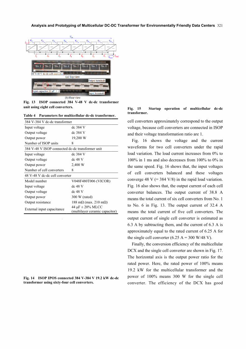
Fig. 13 ISOunit using eig
Table 4 Par
384 V-384 V
Input voltage
Output voltag
Output power
Number of IS
384 V-48 V I
Input voltage
Output voltag
Output power
Number of ce
48 V-48 V dc
Model numbe
Input voltage
Output voltag
Output power
Output resista
External inpu
Fig. 14 ISOtransformer u
s and Prototy
OP connected ght cell convert
rameters for m
dc-dc transform
ge
r
SOP units
ISOP connected
ge
r
ell converters
c-dc cell conver
er
ge
r
ance
ut capacitance
P IPOS conneusing sixty-fou
yping of Mult
384 V-48 V ters.
multicellular dc
mer
dc 384 V
dc 384 V
19,200 W
8
d dc-dc transfor
dc 384 V
dc 48 V
2,400 W
8
rter
V048F480T
dc 48 V
dc 48 V
300 W (rate
188 mΩ (ma44 μF ± 20%(multilayer
ected 384 V-38ur cell converte
ticellular DC-
dc-dc transfor
c-dc transform
rmer unit
T006 (VICOR)
ed)
ax. 210 mΩ)% MLCC ceramic capaci
4 V 19.2 kW ders.
DC Transform
rmer
er.
tor)
dc-dc
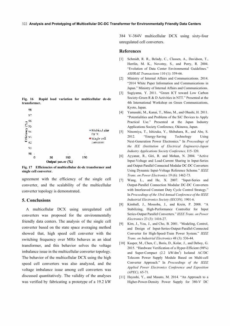
Fig.tran
cell
volt
and
F
wav
load
100
the
of
con
Fig
con
mea
to N
mea
outp
6.3
app
the
F
DC
The
rate
19.2
pow
con
mer for Envir
. 15 Startnsformer.
l converters a
tage, because
d their voltage
Fig. 16 sho
veforms for
d variation. T
0% in 1 ms an
same speed.
cell conver
nverge 48 V (
. 16 also show
nverter balan
ans the total c
No. 6 in Fig
ans the total
put current o
A by subtrac
proximately e
single cell co
Finally, the co
X and the sin
e horizontal a
ed power. He
2 kW for th
wer of 100%
nverter. The
ronmentally F
tup operation
approximately
e cell converte
e transformat
ows the vo
two cell co
The load curr
nd also decre
Fig. 16 show
rters balanc
(= 384 V/8) in
ws that, the o
nces. The ou
current of six
g. 13. The o
current of
of single cell
cting them, a
equal to the ra
onverter (6.25
onversion effi
ngle cell conv
axis is the ou
ere, the rated
he multicellu
% means 300
efficiency
Friendly Data
n of multic
y correspond
ers are conne
ion ratio are
oltage and
nverters und
rent increases
eases from 10
ws that, the in
ed and the
n the rapid lo
output curren
utput current
cell converter
output curren
five cell con
converter is
and the curren
ated current o
5 A = 300 W/
ciency of the
verter are show
utput power
d power of
ular transform
0 W for the
of the DCX
Centers 321
ellular dc-dc
to the output
ected in ISOP
1.
the current
der the rapid
s from 0% to
00% to 0% in
nput voltages
ese voltages
oad variation.
t of each cell
t of 38.8 A
rs from No. 1
nt of 32.4 A
nverters. The
estimated as
nt of 6.3 A is
of 6.25 A for
/48 V).
multicellular
wn in Fig. 17.
ratio for the
100% means
mer and the
e single cell
X has good
c
t
P
t
d
o
n
s
s
.
l
A
A
e
s
s
r
r
.
e
s
e
l
d
Analysi
322
Fig. 16 Ratransformer.
Fig. 17 Efficsingle cell con
agreement
converter, a
converter top
5. Conclus
A multic
converters
friendly data
converter ba
showed tha
switching fr
transformer,
imbalance is
The behavio
speed cell
voltage imb
discussed qu
was verified
s and Prototy
apid load va
ciencies of mulnverter.
with the ef
and the sca
pology is dem
sions
cellular DC
was propos
a centers. Th
ased on the s
at, high spe
requency ove
, and this b
ssue in the mu
or of the mult
converters w
balance issue
uantitatively.
d by fabricati
yping of Mult
riation for m
lticellular dc-d
fficiency of
lability of t
monstrated.
CX using u
ed for the
he analysis o
state space av
eed cell con
er MHz beh
behavior sol
ulticellular co
ticellular DC
was also an
e among cell
The validity
ing a prototy
ticellular DC-
multicellular d
dc transformer
the single
the multicell
unregulated
environment
of the single
veraging met
nverter with
aves as an i
lves the vol
onverter topol
CX using the h
nalyzed, and
l converters
y of the anal
ype of a 19.2
DC Transform
dc-dc
r and
cell
lular
cell
tally
cell
thod
the
ideal
ltage
logy.
high
the
was
lyses
kW
384
unr
Re
[1]
[2]
[3]
[4]
[5]
[6]
[7]
[8]
[9]
[10]
[11]
mer for Envir
4 V-384V m
egulated cell
ferences
Schmidt, R.
Herrlin, M.
“Evolution o
ASHRAE Tra
Ministry of I
“2014 White
Japan.” Minis
Sugiyama, Y
Society-Gree
4th Internatio
Kyoto, Japan
Yamasaki, M
“Potentialitie
Practical U
Applications
Ninomiya, T
2012. “E
Next-Generat
the IEE (In
Industry App
Ayyanar, R.
Input-Voltage
and Output-Pa
Using Dynam
Trans. on Pow
Wang, L.,
Output-Parall
with Interleav
In Proceeding
Industrial Ele
Kimball, J.,
Stabilizing,
Series-Outpu
Electronics 2
Kim, J., You
and Design
Converter fo
Trans. on Ind
Kasper, M., C
2015. “Hardw
and Super-C
Telecom Pow
Converter A
Applied Pow
(APEC), 65-7
Hayashi, Y.,Higher-Powe
ronmentally F
multicellular
converters.
R., Belady, C
K., Novotny
of Data Center
ansactions 110 (
Internal Affairs
e Paper Informa
stry of Internal
Y. 2011. “Gree
en R & D Activi
onal Workshop
n.
M., Kanai, T., M
es and Problems
se.” Presented
Society Confer
T., Ishizuka, Y.
Energy-Saving
tion Power Ele
nstitution of
lications Societ
, Giri, R. and
e and Load-Cu
arallel Connecte
mic Input-Volta
wer Electronics
and He, X
lel Connection
ved Constant D
gs of the 33rd A
ectronics Socie
Mossoba, J.,
High-Performa
ut Parallel Conv
23 (3): 1416-27.
u, J., and Cho,
of Input-Seri
or High-Speed-
dustrial Electro
Chen, C., Boris
ware Verificatio
Compact (2.2
wer Supply M
Approach.” In
wer Electronics
71.
and Masato, Mer-Density Pow
Friendly Data
DCX usin
., Classen, A.,
, S., and Pe
r Environmenta
(1): 559-66.
s and Commun
ation and Com
Affairs and Co
en ICT toward
ities in NTT.” P
p on Green Co
Mino, M., and O
s of the SiC De
d at the Ja
rence, Okinawa
., Shibahara, R
Technolo
ectronics.” In P
Electrical En
ty Conference, I
d Mohan, N.
urrent Sharing
ed Modular DC-
age Reference S
s 19 (6): 1462-7
X. 2007. “Inp
Modular DC-D
Duty Cycle Con
Annual Conferen
ty (IECON), 19
, and Krein,
ance Controll
erters.” IEEE T
.
B. 2001. “Mod
ies-Output-Para
-Train Power S
nics 48 (3): 536
, D., Kolar, J.,
on of a Hyper-E
kW/dm3) Iso
Module Based
Proceedings
s Conference a
M. 2014. “An wer Supply fo
Centers
ng sixty-four
Davidson, T.,
erry, R. 2004.
al Guidelines.”
nications. 2014.
mmunications in
ommunications.
d Low Carbon
Presented at the
ommunications,
hashi, H. 2011.
evices to Apply
apan Industry
a, Japan.
R., and Abe, S.
ogy Using
Proceedings of
gineers)-Japan
I15- I20.
2004. “Active
in Input-Series
-DC Converters
Scheme.” IEEE
73.
put-Series and
DC Converters
ntrol Strategy.”
nce of the IEEE
901-6.
P. 2008. “A
ler for Input
Trans. on Power
deling, Control,
allel-Connected
System.” IEEE
6-44.
and Deboy, G.
Efficient (98%)
olated AC/DC
on Multi-cell
of the IEEE
and Exposition
Approach to aor 380-V DC
r
,
.
”
.
n
n
e
,
.
y
y
.
g
f
n
e
s
s
E
d
s
”
E
A
t
r
,
d
E
.
)
C
l
E
n
a C

Analysis and Prototyping of Multicellular DC-DC Transformer for Environmentally Friendly Data Centers
323
Distribution System.” Electrical Engineering in Japan 186 (3): 51-62.
[12] Tolbert, L. M., Ozpineci, B., Islam, S. K., and Chinthavali, M. S. 2003. “Wide Bandgap Semiconductors for Utility Applications.” In Proceedings of the IASTED (International Association of Science and Technology for Development) International Conference on PES (Power and Energy Systems) 2003, 317-21.
[13] Erickson, W., and Maksimovic, W. 2001. Fundamentals of Power Electronics. New York: Springer US.
[14] Middlebrook, R., and Cuk, S. 1976. “General Unified Approach to Modeling Switching-Converter Power Stages.” In Proceedings of the IEEE Power Electronics Specialist Conference (PESC), 18-34.
[15] Ninomiya, T., Nakahara, M., Higashi, T., and Harada, K. 1991. “Unified Analysis of Resonant Converters.” IEEE Trans. on Power Electronics 6 (2): 260-70.
[16] Japanese Electro-technical Committee. 1995. “Impulse Voltage and Current Tests in General.” Japanese Electro-technical Committee.