analog design in sub-100nm technologies
TRANSCRIPT


2
History
?
Pederson/Wooley, ca. 1970
Wooley/Boser, ca. 1988
Boser/Murmann, ca. 2003
?
Pederson, ca. 1951

3
Outline
Impact of scaling on analog performance metrics
How to improve analog performance using digital gates
Digitally assisted A/D converters

4
Quotes[Vertregt, ESSCIRC 2004]
"Significant power efficiency improvements are predicted as a result of scaling to deep sub-micron technology nodes."
[Annema, IEEE J. Solid-State Circuits, 12/2005 ]"In summary: unlike digital designs, analog circuits can benefit from technology scaling if the supply voltages are not scaled down."
[Nauta, ESSCIRC 2005]"The evolution of CMOS technology will continue for many years to come, which is beneficial for digital circuits but which is not so for analog."

5
List of ConcernsReduced supply voltage
Low intrinsic gain
Variability
Distortion
Gate leakage
Isolation
…
Cost (mask & wafer)
Model accuracy
…

6
Technology Benchmarking
gs
mT C
g21fπ
=Transit frequency
Transconductorefficiency
Available signal swing
Intrinsic gain
D
mIg
ds
mgg

7
gm/ID and fT trends
gm/IDessentially unaffected by scaling
Very high fTin recent technologies
Enables RF CMOS
-0.4 -0.2 0 0.2 0.4 0.60
200
400
600
800
1000
1200(b)
VGS-Vt [V]
(gm
/I D)*
f T [GH
z*S
/A]
-0.2 -0.1 0 0.1 0.2 0.3 0.4 0.5 0.60
10
20
30
40(a)
g m/I D
[S/A
]
VGS-Vt [V]-0.2 -0.1 0 0.1 0.2 0.3 0.4 0.5 0.6
0
40
80
120
160
f T [GH
z]
180nm130nm90nm
180nm130nm90nm

8
Available Signal Swing
0
1
2
3
4
5
0.50um 0.35um 0.25um 0.18um 0.12um 90nm 65nm 45nm 32nm
Technology Node
V DD [V
]
> 4kT/q
> 4kT/q
VDD
qkT8V SwingAvailable DD −<

9
Noise Limited Circuit Performance
C/kTSwingDR
Cg
BWIVP2
mDDD ∝∝⋅∝
D
m2
DDDD I
gVSwingV
PDRBW
⋅⎟⎟⎠
⎞⎜⎜⎝
⎛⋅∝
⋅
Low VDD is generally bad news, butAnalog designers have worked hard to maintain or even improve Swing/VDD
Typical ADC in 0.5μm: Swing/VDD=2/5Typical ADC in 90nm: Swing/VDD=0.5/1
How about gm/ID?

10
Leveraging fT
ExamplefT = 50GHz, 130nm: gm/ID = 8S/A, 90nm: gm/ID = 16S/A
For "fixed-speed" applications, high fT can be leveraged to mitigate low VDD penalty
-0.2 -0.1 0 0.1 0.2 0.3 0.4 0.5 0.60
10
20
30
40g m
/I D [S
/A]
VGS-Vt [V]-0.2 -0.1 0 0.1 0.2 0.3 0.4 0.5 0.6
0
40
80
120
160
f T [GH
z]
180nm130nm90nm

11
Further ConsiderationsAnalog building blocks are never completely limited by thermal noise
Not uncommon to have ~50% dynamic powerDecreases with scaling
Designers are continuing to develop/refine low-voltage design techniques
Recent publications show very good analog building block performance at 1V
Bottom lineAnalog design is challenging at 1V, but it's neither impossible nor detrimental

12
Intrinsic GainA real issue
How to design a high-gain op-amp with devices that have intrinsic gain of ~10?
How much worse does this get at 45nm/65nm?
0 0.2 0.4 0.6 0.8 1 1.2 1.4 1.60
50
100
150
200
250(a)
VDS [V]
I D [ μ
A]
0 0.2 0.4 0.6 0.8 1 1.2 1.4 1.60
10
20
30
40
50(b)
VDS [V]
g m/g
ds
180nm130nm90nm
180nm130nm90nm
(VGS-Vt=100mV)

13
Intrinsic Gain in the Near Future
Pretty bad…
SolutionsUse non-minimum length device (NML-device)Use asymmetric device without drain-side pocket implant (A-device)Or, don't try to build op-amps in these technologies…
More later
0 0.2 0.4 0.6 0.8 10
5
10
15
VDS [V]
g m/g
ds45nm (TCAD)65nm (TCAD)90nm (BSIM4)(VGS-Vt=100mV)

14
Intrinsic Gain of Alternate Devices (45nm)
For both NML and A-device Lphysical=80nm (Lphysical=24nm for minimum length device)
Great, lots of gain!But how about fT?
(VGS-Vt=100mV)
0 0.2 0.4 0.6 0.8 10
50
100
150( )
VDS [V]
g m/g
dsMin. lengthNML-deviceA-device
(VGS-Vt=100mV)

15
gm/ID and fT for Alternate Devices (45nm)fT much lower than for minimum length 45-nm device
But still better than minimum length device in 90nm…
Who needs fT > 200GHz in an op-amp…?
-0.2 -0.1 0 0.1 0.2 0.3 0.4 0.50
1000
2000
3000
4000
5000(b)
VGS-Vt [V]
(gm
/I D)*
f T [GH
z*S
/A]
-0.2 -0.1 0 0.1 0.2 0.3 0.4 0.50
10
20
30
40(a)
VGS-Vt [V]
g m/I D
[S/A
]
-0.2 -0.1 0 0.1 0.2 0.3 0.4 0.50
200
400
600
800
f T [GH
z]
Minimum lengthNML-deviceA-device
Minimum lengthNML-deviceA-device

16
Variability (1)
[Courtesy A. Bowling, Texas Instruments]

17
Variability (2)
Device mismatch larger than process corner variations!For small "digital" transistors…
[Marcel Pelgrom, Philips]

18
Variability (3)Analog
A well known problemDesigners are used to "caring" about mismatch
Lots of options and potential solutions
Layout techniques, analog or digital calibration, dynamic element matching, larger device area, …
Usually care about matching for a few up to a few hundred transistors
Digital
A "new" problemSignificant impact on achievable performance, yield, design methodology, EDA, …
Big difference compared to analog
Care about millions if not billions of devices!

19
Outline
Impact of scaling on analog performance metrics
How to improve analog performance using digital gates
Digitally assisted A/D converters

20
"Mostly Digital" or "Digitally Assisted" Analog
Based on minimalistic analog circuits
Achieve precision/performance by means of added digital processing
ExamplesMostly digital PLLsPower amplifiers with digital pre-distortionDigital radio processor architecture (TI)Digitally corrected ADCs…

21
Motivation from Energy PerspectiveDoes "digital assistance" make sense?
Interesting metric to look atHow many digital gates can you toggle for the energy needed in one A/D conversion?
ExampleTwo-input NAND gate in 90nm CMOS consumes2.5 fJ/operation10-bit ADC consumes 0.25 nJ/conversionEnergy equivalent number of gates
0.25nJ/2.5fJ = 100,000

22
Impact of Technology Scaling
0
50000
100000
150000
200000
250000
300000
350000
0.00.10.20.30.40.50.60.70.8Feature Size L [μm]
Ener
gy E
quiv
alen
t Num
ber o
f Gat
es6 bits
8 bits
10bits12 bits
14 bits
16 bits

23
Leveraging Digital Assistance (1)
Power Dissipation
Speed
Matching LinearityNoise
PrecisionNon-Fundamental

24
Leveraging Digital Assistance (2)Can correct deterministic, repeatable error using digital processor
Important considerationsImpractical to correct for arbitrary errors
Must limit "sloppiness" through judicious analog design
Must be able to adjust correction functions over time
Errors will depend on operating conditions, circuit age, etc.

25
Example: Pipeline ADC
Bottleneck: Highly linear gain element

26
Open-Loop Gain Element
+ Lower noise
+ Increased signal range
+ Lower power
+ Faster
– NonlinearUse post-processor to linearize!
Open-Loop AmplifierConventional Precision Amplifier

27
Digital Nonlinearity Correction
Calibration of digital inverse is accomplished by adjusting parameters such that signal statistics at output are independent of Vmod
Algorithm continuously tracks variations in amplifier polynomial

28
Proof of Concept Prototype
Open-loop amplifier only in first, most critical stageAmplifier power savings ~4x
Judicious analog/digital co-designOnly two corretion parameters (linear and cubic amplifier error)
~8000 Gates
[Murmann, JSSC 12/2003]
29
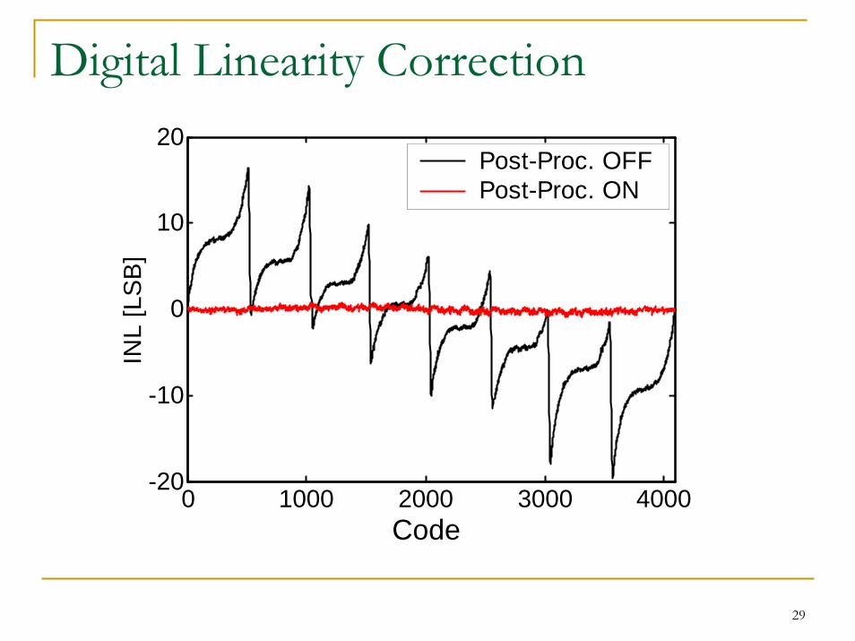
Digital Linearity Correction
0 1000 2000 3000 4000-20
-10
0
10
20
Code
INL
[LS
B]
Post-Proc. OFFPost-Proc. ON
Code

30
Amplifier Waveforms
Typically settle to within small % error of final value
Most of IBIAS is shunted to ground through the amplifier for t>2τ

31
Exploiting Incomplete Settling
IdeaSettle for only 1.5τ to improve power efficiency (or speed)Use digital processing to correct for settling error (in addition to nonlinearity)
Volta
ge
0 2 4 6 8 10t/τ
Cur
ren t
IBIAS
SavingsIload
Vout
Incomplete Settling Conventional
32
00.5
11.5
22.5
33.5
44.5
0.1 1 2 3 4 5 6 7 8 9 10t/τ
Nor
mal
ized
1 Pow
er E
ffici
ency
0
Power Efficiency versus Settling
Assumptions:• kT/C noise limited• Constant
conversion rate
Optimal settling is around 1τ-1.5τ
1Normalized to power at 10τ settling.

33
Proof of Concept Circuit
Judicious analog design ensures that incomplete settling error is linear (or only weakly nonlinear)
Very easy to correct!
Vin1p
Vrefp
16
φ1
Col
16
Vcm
φ1e
Vcm
φconnect
open-loopamp
Vcm
φshort
φ2
Vcm
φ2e
*
* *
* = additional switches for glitch suppression
Vres1pVxpC2p
Stage 1 Stage 2 φ1e, φ1
φ2e, φ2
Dn
Vrefn
Dn
16
Dp
Dp
φshort
φconnectΔt
Vres1(Vres1p-Vres1n)
tsample
w/ additionalswitches
w/o additionalswitches
C1p[15:0]
Col Vres1n
[Iroaga & Murmann, VLSI 2006]

34
Pipeline Stage Power Breakdown
0
10
20
30
40
50
Pow
er [m
W]
AD9235 Open-Loop Open-Loop &Incomplete
Settling
FlashBiasingGmPost-Proc.
4x 16x
(0.35μm)

35
Calibration Problem RevisitedThe "sloppier" we make the analog portion of the ADC, the more parameters we need to estimate and track
Can become quite complex or even impossible without disturbing normal ADC operation
Idea: "System Embedded" postprocessing and calibration of ADC
Leverage redundancy and knowledge of certain input signal properties to estimate ADC errorsRe-use existing system resources for ADC calibration

36
Embedded ADC Calibration for OFDM
Communications protocol uses "pilot tones" to measure and equalize RF channel nonidealities
Why not use these pilots to "equalize" ADC?Errors in pilot signals can be used to estimate correction parameters for sloppy ADC
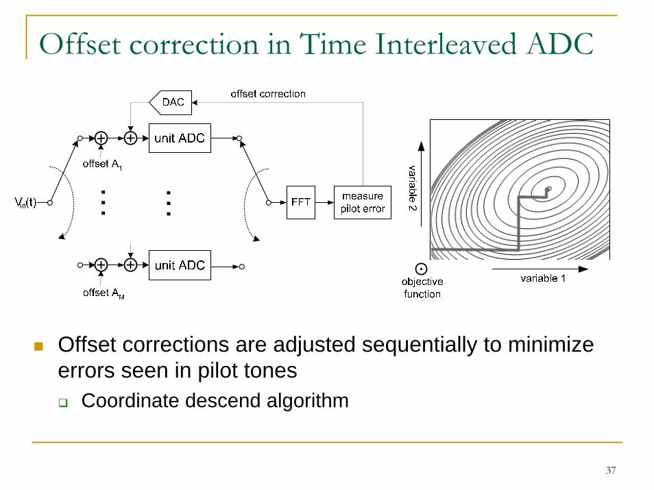
Example: Offset correction in time interleaved ADC
[Oh and Murmann, to appear, IEEE TCAS1]
37
Offset correction in Time Interleaved ADC
Offset corrections are adjusted sequentially to minimize errors seen in pilot tones
Coordinate descend algorithm

38
Typical Learning Curve
Steady state ripple due to communication channel noiseTradeoff: Ripple versus convergence rate
ENOB ≅ 5.8bits in AWGN channel with SNR = 20dB
~100ms

39
Comparator Circuit
Fully differential architecture
Low gain/low power pre-amp, primarily for common mode rejection
Dynamic latch with positive feedback for fast comparison

40
Pre-amp with Offset Adjustment
Offset DACCurrent modeOffset correction range ±8 LSB
Pre-amp Low gain (~2)CMRR > 20

41
Dynamic Latch
Calibration allows use of near minimum width devices for low power

42
Layout
Core area: 640μm x 550μm (0.18μm CMOS)
(a) ADC Core (b) full chip

43
Estimated Power (Post-Layout)500MS/s, 6-bit ADC
Power (mW)
Digital 9.0
Analog 3.6
Clock 3.6
Calibration(estimated) 0.4
Total 16.6

44
An Interesting Hike Lies Ahead…
Bag of Tricks
A
D

45
Cost – The "Real" End of The Roadmap?
Reference point: 30 mm2 die in 0.12μm CMOS
[Marcel Pelgrom, Philips][Marcel Pelgrom, Philips]

46
ConclusionsAnalog design in modern IC technologies is and always will be challenging
This is what keeps our job interesting…
New technologies means new solutionsMust continue to develop low voltage design techniquesMust continue to leverage digital capabilities for analog performance enhancements
Based on current roadmap, there is no fundamental reason why analog couldn't be implemented in "digital" technologies of the near future
Interesting questionsWill high performance digital circuits survive scaling?Can the IC industry continue to benefit from scaling despite thelarge anticipated wafer & mask costs?

47
Acknowledgements
Graduate StudentsYangjin Oh, Echere Iroaga, Jason Hu, Justin Kim, Pedram Lajevardi, Wei Xiong, Clay DaigleParastoo Nikaeen (Co-advising with Prof. Dutton)
Sponsors