an insight into the charge carriers transport properties
TRANSCRIPT
HAL Id: hal-02947932https://hal.archives-ouvertes.fr/hal-02947932
Submitted on 30 Sep 2020
HAL is a multi-disciplinary open accessarchive for the deposit and dissemination of sci-entific research documents, whether they are pub-lished or not. The documents may come fromteaching and research institutions in France orabroad, or from public or private research centers.
L’archive ouverte pluridisciplinaire HAL, estdestinée au dépôt et à la diffusion de documentsscientifiques de niveau recherche, publiés ou non,émanant des établissements d’enseignement et derecherche français ou étrangers, des laboratoirespublics ou privés.
An insight into the charge carriers transport propertiesand electric field distribution of CH 3 NH 3 PbBr 3
thick single crystalsOriane Baussens, Loli Maturana, Smaïl Amari, Julien Zaccaro, Jean-Marie
Verilhac, Lionel Hirsch, Eric Gros-Daillon
To cite this version:Oriane Baussens, Loli Maturana, Smaïl Amari, Julien Zaccaro, Jean-Marie Verilhac, et al.. An insightinto the charge carriers transport properties and electric field distribution of CH 3 NH 3 PbBr 3 thicksingle crystals. Applied Physics Letters, American Institute of Physics, 2020, 117 (4), pp.041904.�10.1063/5.0011713�. �hal-02947932�

AUTHOR QUERY FORM
Journal: Appl. Phys. Lett.
Article Number: APL20-AR-03618
Please provide your responses and any corrections
by annotating this PDF and uploading it to AIP’s
eProof website as detailed in the Welcome email.
Dear Author,
Below are the queries associated with your article; please answer all of these queries before sending the proof back to AIP.
Article checklist: In order to ensure greater accuracy, please check the following and make all necessary corrections before returning yourproof.
1. Is the title of your article accurate and spelled correctly?
2. Please check affiliations including spelling, completeness, and correct linking to authors.
3. Did you remember to include acknowledgment of funding, if required, and is it accurate?
Location inarticle
Query / Remark: click on the Q link to navigateto the appropriate spot in the proof. There, insert your comments as a PDF annotation.
AQ1 Please check that the author names are in the proper order and spelled correctly. Also, please ensure that eachauthor’s given and surnames have been correctly identified (given names are highlighted in red and surnamesappear in blue).
AQ2 Please check and confirm presentation of affiliation 3.
AQ3 Please provide complete details for Ref. 2.
AQ4 Please provide volume and page number for Ref. 4.
AQ5 Please provide publisher name for Ref. 13.
AQ6 Please provide book title for Ref. 14.
Please confirm ORCIDs are accurate. If you wish to add an ORCID for any author that does not have one, you may do sonow. For more information on ORCID, see https://orcid.org/.
Oriane Baussens - 0000-0003-0042-2855
Loli Maturana - 0000-0002-4324-123X
Sma€ıl Amari - 0000-0002-5565-9481
Julien Zaccaro-
Jean-Marie Verilhac-
Lionel Hirsch - 0000-0003-2325-5535
Eric Gros-DAillon - 0000-0002-4196-7854
Please check and confirm the Funder(s) and Grant Reference Number(s) provided with your submission:
Horizon 2020 Framework Programme, Award/Contract Number 777222
Please add any additional funding sources not stated above:
Thank you for your assistance.
PROOF COPY [APL20-AR-03618]
1 An insight into the charge carriers transport2 properties and electric field distribution3 of CH3NH3PbBr3 thick single crystals
5 Cite as: Appl. Phys. Lett. 117, 000000 (2020); doi: 10.1063/5.00117136 Submitted: 30 April 2020 . Accepted: 30 June 2020 .7 Published Online: 0 Month 0000
8
910AQ1 Oriane Baussens,1,a) Loli Maturana,1 Sma€ıl Amari,2 Julien Zaccaro,3 Jean-Marie Verilhac,2 Lionel Hirsch,4
11and Eric Gros-DAillon1,a)
12 AFFILIATIONS
13 1University Grenoble Alpes, CEA, LETI, F38000 Grenoble, France14 2University Grenoble Alpes, CEA, LITEN, F38000 Grenoble, France15 3University Grenoble Alpes, CNRS, Grenoble INP, Institut N�eel, BP166, 38042 Grenoble, Cedex 09, FranceAQ216 4University Bordeaux, IMS-CNRS, UMR 5218, Bordeaux INP, ENSCBP, F33405 Talence, France
17 a)Authors to whom correspondence should be addressed: [email protected] and [email protected]
ABSTRACT
18 Thanks to their unique combination of semiconducting properties and a large cross section for energetic photons, metal halide perovskites19 could theoretically achieve high x-ray to charge carriers conversion rates, making them materials of high interest for the direct x-ray20 detection. In this work, we focus on the transport properties of methylammonium lead tribromide (MAPbBr3) single crystals. Time of Flight21 measurements and x-ray focused experiments along the edge of the samples were carried out. We report homogenous holes transit through-22 out the thickness of the samples as well as poor electrons transit. We also report the continuity of the electric field throughout the thickness23 of the MAPbBr3 samples, and we present preliminary fitting results to discuss its nature.
Published under license by AIP Publishing. https://doi.org/10.1063/5.0011713
24 Semiconducting metal halide perovskites have gained a lot of25 interest for solar cells applications. In the last decade, the reported effi-26 ciency perovskite based solar cells has increased from 3.81% to27 25.2%.1,2 However, the main concern for such mainstream application,28 as mentioned by Li et al., is the presence of heavy metals in the ionic29 crystal.3 On the other hand, heavy atoms like lead have large x-rays30 cross sections. Therefore, heavy metal halide perovskites could be31 perfectly suited for confined applications such as direct x-ray detectors32 for medical imaging. In addition to the cross section, efficient x-ray33 detection also requires good charge carriers’ transport properties in34 order to optimize charge collection and reduce ghosting effect.35 In this work, we investigated the photocarriers’ transport proper-36 ties of thick methylammonium lead tribromide (MAPbBr3) single37 crystals. We studied the electron and hole mobilities with laser Time38 of Flight. The continuity of the electric field throughout the thickness39 of the samples was then tested by x-ray focused experiments, the first40 to be reported to our knowledge.41 Several MAPbBr3 single crystals of controlled quality were grown42 individually by a seeded Inverse Temperature Crystallization method.43 The growth procedure and crystal quality are detailed in a previous
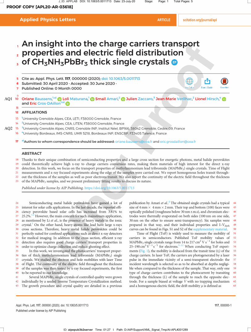
44publication by Amari et al..4 The obtained single crystals had a typical45size of 4mm� 4mm� 2mm. Their top and bottom (100) faces were46optically polished (roughness below 30nm r.m.s), and chromium elec-47trodes were thermally evaporated on both sides (100nm on one side,4830 nm on the other to ensure semi-transparency). Six samples were49prepared in that way, and their individual properties and I–Vdark50curves can be found in Figs. S1 and S2 of the supplementary material.51Time of Flight (ToF) is widely used to measure the mobility of52carriers in semiconductors. Published ToF mobility values of53MAPbBr3 single crystals range from 14 to 217 cm2 V s�1 for holes and5425–190 cm2V�1 s�1 for electrons.5–12 When conducting ToF experi-55ments (Fig. 1), the mobility is deduced from the transit time (tt) of the56charge carriers. In laser ToF, the carriers are photogenerated by a laser57pulse in the immediate vicinity of a semi-transparent electrode: the58incident wavelength is selected so as to be absorbed at depths negligi-59ble when compared to the thickness of the sample. That way, only one60type of charge carriers contributes to the photocurrent by transiting61through the thickness (L) of the sample to reach the opposite elec-62trode. For a sample biased at voltage V with no trapping mechanism63and a homogenous electric field, the drift mobility l is defined as
J_ID: APPLAB DOI: 10.1063/5.0011713 Date: 23-July-20 Stage: Page: 1 Total Pages: 5
ID: aipepub3b2server Time: 01:27 I Path: D:/AIP/Support/XML_Signal_Tmp/AI-APL#201289
Appl. Phys. Lett. 117, 000000 (2020); doi: 10.1063/5.0011713 117, 000000-1
Published under license by AIP Publishing
Applied Physics Letters ARTICLE scitation.org/journal/apl
PROOF COPY [APL20-AR-03618]
l ¼ L2= V�ttð Þ cm2 � V�1 � s�1ð Þ: (1)
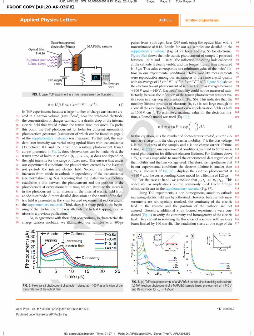
In ToF experiments, because a large number of charge carriers are cre-64 ated in a narrow volume (�10�2 cm3) near the irradiated electrode,65 the concentration of charges can lead to a drastic drop of the internal66 electric field that would reduce the transit time measured. To probe67 this point, the ToF photocurrent for holes for different amounts of68 photocarriers generated (estimation of which can be found in page 269 of the supplementary material) was measured. To that end, the inci-70 dent laser intensity was varied using optical filters with transmittance71 (T) between 0.1 and 0.5. From the resulting photocurrent transit72 curves presented in Fig. 2, three observations can be made. First, the73 transit time of holes in sample 1 (tt-hþ � 7.5ls) does not depend on74 the light intensity for the range of fluxes used. This ensures that under75 our experimental conditions the photocarriers created by the laser do76 not perturb the internal electric field. Second, the photocurrent77 increases from anode to cathode independently of the transmittance78 (see normalized Fig. S3). Knowing that the instantaneous mobility79 establishes a link between the photocurrent and the position of the80 photocarriers at every moment in time, we can attribute the increase81 in the photocurrent to an increase in the internal electric field from82 anode to cathode. A more detailed discussion on the nature of the elec-83 tric field is presented in the x-ray focused experimental section and in84 the supplementary material. Third, there is a sharp peak at the begin-85 ning of the photocurrent. It was attributed it to fast trapping mecha-86 nisms in a previous publication.13
87 So, in agreement with these first observations, to characterize the88 charge carriers mobility, we illuminated our samples with 800 ps
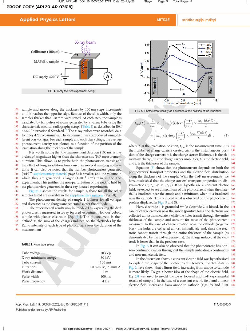
89pulses from a nitrogen laser (337 nm), using the optical filter with a90transmittance of 0.16. Results for our six samples are detailed in the91supplementary material (Fig. S4 for holes and Fig. S5 for electrons).92Figure 3(a) shows the hole transit photocurrent of sample 1 polarized93between �60V and �140V. The inflection indicating hole collection94at the cathode is clearly visible, and the longest transit time measured95is 13ls. This value corresponds to a minimum value of the holes’ life-96time in our experimental conditions. Holes’ mobility measurements97were reproducible among our six samples of the same crystal quality98with an average of 13 cm2 V�1 s�16 2 cm2V�1 s�1. Figure 3(b) shows99the electron transit photocurrent of sample 1 for bias voltages between100þ100V and þ140V. Electrons’ mobility could not be measured satis-101factorily, because the inflection of the transit photocurrent was not vis-102ible even in a log –log representation (Fig. S6). This indicates that the103mobility lifetime product of electrons (le-se-) is not large enough to104allow all the electrons to fully transit even at polarization fields as high105as 1500V cm�1. To estimate a maximal value for the electrons’ life-106time, a Ramo’s model was used [Eq. (2)]:
i tð Þ ¼ n e lV � exp � ts
� �=L2: (2)
107In this equation, n is the number of photocarriers created, e is the ele-108mentary charge, l is the charge carrier mobility, V is the bias voltage,109L is the thickness of the sample, and s is the charge carrier lifetime.110Using Eq. (2) and our experimental conditions, we tried to fit the mea-111sured photocurrent for different electron lifetimes. For lifetimes above1121.25ls, it was impossible to model the experimental data regardless of113the mobility and the bias voltage used. Therefore, we hypothesize that114in our experimental conditions the electron lifetime is smaller than1151.25ls. The inset of Fig. 3(b) displays the electron photocurrent at116þ140V and the corresponding Ramo model for a lifetime of 1.25ls.117For the case at hand, we conclude that le-se- � lhþshþ. This118conclusion as implications on the commonly used Hecht fittings,119which we discuss in the supplementary material (Fig. S7).120Using ToF experiments, a non-homogenous, anode to cathode121increasing electric field was hypothesized. However, because ToF mea-122surements are not spatially resolved, the continuity of the electric123field in the volume and the position of the cathode are not124assured. Therefore, additional x-ray focused experiments were con-125ducted (Fig. 4) to verify the continuity and homogeneity of the electric126field. They consist in scanning the thickness of a sample with an x-ray127beam limited by 100lm slit. The irradiation starts at one edge of the
FIG. 1. Laser ToF experiment in a hole measurement configuration.
FIG. 2. Hole transit photocurrent of sample 1 biased at �100 V as a function of thetransmittance of the optical filter.
FIG. 3. (a) ToF hole photocurrent of a MAPbBr3 sample (inset: mobility calculation).(b) ToF electron photocurrent of a MAPbBr3 sample (inset: photocurrent at þ140 Vand Ramo model for se- ¼ 1.25ls).
J_ID: APPLAB DOI: 10.1063/5.0011713 Date: 23-July-20 Stage: Page: 2 Total Pages: 5
ID: aipepub3b2server Time: 01:27 I Path: D:/AIP/Support/XML_Signal_Tmp/AI-APL#201289
Applied Physics Letters ARTICLE scitation.org/journal/apl
Appl. Phys. Lett. 117, 000000 (2020); doi: 10.1063/5.0011713 117, 000000-2
Published under license by AIP Publishing
PROOF COPY [APL20-AR-03618]
128 sample and moves along the thickness by 100lm steps increments129 until it reaches the opposite edge. Because of the slit’s width, only the130 samples thicker than 0.8mm were tested. At each step, the sample is131 irradiated by ten pulses of x-rays generated by a varian tube using the132 characteristic medical radiography setups (Table I) as described in IEC133 62220 International Standard.14 The x-ray pulses were recorded via a134 Keithley 428 picoammeter. The experiment was reproduced using dif-135 ferent bias voltages. For each sample and each bias voltage, the average136 photocurrent density was plotted as a function of the position of the137 irradiation along the thickness of the sample.138 It is worth noting that the measurement duration (100ms) is five139 orders of magnitude higher than the characteristic ToF measurement140 duration. This allows us to probe both the photocarriers transit and141 the effect of long irradiation times used in medical imaging applica-142 tions. It can also be noted that the number photocarriers generated143 (�1010, supplementary material page 5) is smaller, and the volume in144 which they are generated is larger (�10�1 cm3) than in the ToF145 experiments. This justifies the non-perturbation of the electric field by146 the photocarriers generated in the x-ray focused experiments.147 Figure 5 shows the results for sample 1, those for all the other148 samples tested are available in the supplementary material (Fig. S8).149 The photocurrent density of sample 1 is linear for all voltages150 and decreases as the charges are generated closer the cathode.151 The experimental results may be modeled by expressing the drift152 photocurrent measured in x-ray focused experiment for our cuboid153 sample with planar electrodes [Eq. (3)]. The photocurrent is then154 defined as the sum of the charges induced on the electrodes by the155 Ramo intensity of each type of photocarriers over the duration of the156 measurement
Imes Xð Þ ¼1tmes�
ðne� x tð Þð Þexp �t
se�
� ��ele�E x tð Þð Þ
Ldt
"
þðnhþ x tð Þð Þexp �t
shþ
� ��elhþE x tð Þð Þ
Ldt
#; (3)
157where X is the irradiation position, tmes is the measurement time, n is158the number of charge carriers created, x(t) is the instantaneous posi-159tion of the charge carriers, s is the charge carrier lifetimes, e is the ele-160mentary charge, l is the charge carrier mobilities, E is the electric field,161and L is the thickness of the sample.162Equation (3) shows that the photocurrent depends on both the163photocarriers’ transport properties and the electric field distribution164along the thickness of the sample. With the ToF measurements, we165have established that the charge carriers’ transport properties are dis-166symmetric (le-se- � lhþshþ). If we hypothesize a constant electric167field, we expect to see a maximum of the photocurrent when the mate-168rial is irradiated near the anode and a minimum when it is irradiated169near the cathode. This is indeed what is observed on the photocurrent170profiles displayed in Figs. 5 and S8.171Here, electrode 1 is grounded while electrode 2 is biased. In the172case of charge creation near the anode (positive bias), the electrons are173collected almost immediately while the holes transit through the entire174thickness of the sample and account for most of the photocurrent175measured. In the case of charge creation near the cathode (negative176bias), the holes are collected almost immediately and, since the elec-177trons cannot transit through the entire thickness of the sample (as178demonstrated by the ToF experiments), the charge induced at the elec-179trode is lower than in the previous case.180In Fig. 5, it can also be observed that the photocurrent has non-181zero continuous values throughout the sample indicating a continuous182and non-null electric field.183In the discussion above, a constant electric field was hypothesized184to explain the shape of the photocurrent. However, the ToF data in185Fig. 2 have shown that a linear field, increasing from anode to cathode186is more likely. To get a better idea of the shape of the electric field,187Eq. (3) was used to model the x-ray focused and ToF experimental188results of sample 1 in the case of a constant electric field and a linear189electric field, increasing from anode to cathode (Figs. S9 and S10).
FIG. 4. X-ray focused experiment setup.
TABLE I. X-ray tube setups.
Tube voltage 70 kVpX-ray minimum energy 50 keVTube current 100mAFiltration 0.8mm Be, 23mm AlWork distance 1mPulse width 100msPulse frequency 4Hz
FIG. 5. Photocurrent density as a function of the position of the irradiation.
J_ID: APPLAB DOI: 10.1063/5.0011713 Date: 23-July-20 Stage: Page: 3 Total Pages: 5
ID: aipepub3b2server Time: 01:27 I Path: D:/AIP/Support/XML_Signal_Tmp/AI-APL#201289
Applied Physics Letters ARTICLE scitation.org/journal/apl
Appl. Phys. Lett. 117, 000000 (2020); doi: 10.1063/5.0011713 117, 000000-3
Published under license by AIP Publishing

PROOF COPY [APL20-AR-03618]
190 We found that the x-ray focused experimental data could be modeled191 by either of those fields. However, only the linear electric field allowed192 modeling the ToF experimental data. This is in contradiction with the193 homogenous electric field hypothesis of Eq. (1). Nonetheless, the use194 of a constant electric field to model our data only leads to a 5% under-195 estimation of the mobility, which is negligible compared to the 15%196 measurement uncertainty. More in depth modeling is under progress197 to achieve better fitting for both types of experimental data.198 In conclusion, we have measured reproducible hole mobility of199 MAPbBr3 single crystals of controlled quality with laser ToF at 13 cm2
200 V�1 s�16 2 cm2 V�1 s�1. We have also seen that both ToF and x-ray201 focused results are consistent with poor electrons’ transport properties202 in MAPbBr3 single crystals. We can only hypothesize that the lack of203 electrons transit is due to either deep trapping levels or recombination204 centers, as shown by Musiienko et al.9 In the case of a deep trapping205 level, the detrapping constant would be higher than 100ms, our typical206 measurement duration. Finally, we have shown that the internal elec-207 tric field exists throughout the thickness of the samples, and our pre-208 liminary modeling results point toward it being linear and increasing209 from anode to cathode. Knowing the nature of the electric field is210 essential and will therefore be the topic of follow-up studies.211
212 See the supplementary material for detailed samples properties,213 ToF and x-ray focused measurements of samples 1–6, discussion about214 Hecht fitting, and discussion about the constant electric field215 hypothesis.216
217 The authors thank Trixell and the ATTRACT project, from218 the European Horizon H2020 (Grant No. 777222, PerXi project),219 for the financial support.
220 DATA AVAILABILITY221 The data that support the finding of this study are available from222 the corresponding authors upon reasonable request.
223 REFERENCES224 1A. Kojima, K. Teshima, Y. Shirai, and T. Miyasaka, “Organometal halide perov-225 skites as visible-light sensitizers for photovoltaic cells,” J. Am. Chem. Soc.226 131(17), 6050–6051 (2009).
2272NREL. Best Research Cell Efficiency �. AQ32283J. Li, H.-L. Cao, W.-B. Jiao, Q. Wang, M. Wei, I. Cantone, J. L€u, and A. Abate,229“Biological impact of lead from halide perovskites reveals the risk of introduc-230ing a safe threshold,” Nat. Commun. 11(1), 310 (2020).2314Amari, S., Verilhac, J.-M., Gros D’Aillon, E., Ibanez, A., and Zaccaro, J.,232“Optimization of the growth conditions for high quality233CH3NH3PbBr3 hybrid perovskite single crystals,” Cryst. Growth Des. �, �234(2020). AQ42355D. Shi, V. Adinolfi, R. Comin, M. Yuan, E. Alarousu, A. Buin, Y. Chen, S.236Hoogland, A. Rothenberger, K. Katsiev et al., “Low trap-state density and long237carrier diffusion in organolead trihalide perovskite single crystals,” Science238347(6221), 519–522 (2015).2396W. Wei, Y. Zhang, Q. Xu, H. Wei, Y. Fang, Q. Wang, Y. Deng, T. Li, A.240Gruverman, L. Cao et al., “Monolithic integration of hybrid perovskite single241crystals with heterogenous substrate for highly sensitive x-ray imaging,” Nat.242Photonics 11(5), 315–321 (2017).2437H. Wei, Y. Fang, P. Mulligan, W. Chuirazzi, H.-H. Fang, C. Wang, B. R. Ecker,244Y. Gao, M. A. Loi, L. Cao et al., “Sensitive x-ray detectors made of methylam-245monium lead tribromide perovskite single crystals,” Nat. Photonics 10(5),246333–339 (2016).2478H. Wei, D. DeSantis, W. Wei, Y. Deng, D. Guo, T. J. Savenije, L. Cao, and J.248Huang, “Dopant compensation in alloyed CH3NH3PbBr3�xClx perovskite249single crystals for gamma-ray spectroscopy,” Nat. Mater. 16(8), 826–833250(2017).2519A. Musiienko, P. Moravec, R. Grill, P. Praus, I. Vasylchenko, J. Pekarek, J.252Tisdale, K. Ridzonova, E. Belas, L. Landov�a et al., “Deep levels, charge trans-253port and mixed conductivity in organometallic halide perovskites,” Energy254Environ. Sci. 12(4), 1413–1425 (2019).25510X. Wang, D. Zhao, Y. Qiu, Y. Huang, Y. Wu, G. Li, Q. Huang, Q.256Khan, A. Nathan, W. Lei et al., “PIN diodes array made of perovskite257single crystal for x-ray imaging,” Phys. Status Solidi RRL 12(10),2581800380 (2018).25911E. Lukosi, T. Smith, J. Tisdale, D. Hamm, C. Seal, B. Hu, and M. Ahmadi,260“Methylammonium lead tribromide semiconductors: Ionizing radiation detec-261tion and electronic properties,” Nucl. Instrum. Methods Phys. Res., Sect. A 927,262401–406 (2019).26312X. Liu, H. Zhang, B. Zhang, J. Dong, W. Jie, and Y. Xu, “Charge transport264behavior in solution-grown methylammonium lead tribromide perovskite265single crystal using a particles,” J. Phys. Chem. C 122(26), 14355–14361266(2018).26713A. Musiienko, J. Pipek, P. Praus, M. Brynza, E. Belas, B. Dryzhakov, M.-H. Du,268M. Ahmadi, and R. Grill, Deciphering the Effect of Traps on the Electronic269Charge Transport Properties of Methylammonium Lead Tribromide Perovskites270(�, 2019). AQ527114International Standard, � (International Electrotechnical Commission,2722003). AQ6
J_ID: APPLAB DOI: 10.1063/5.0011713 Date: 23-July-20 Stage: Page: 4 Total Pages: 5
ID: aipepub3b2server Time: 01:27 I Path: D:/AIP/Support/XML_Signal_Tmp/AI-APL#201289
Applied Physics Letters ARTICLE scitation.org/journal/apl
Appl. Phys. Lett. 117, 000000 (2020); doi: 10.1063/5.0011713 117, 000000-4
Published under license by AIP Publishing