photogeneration, transport and recombination of charge ... · photogeneration, transport and...
TRANSCRIPT

1
Photogeneration, Transport and Recombination of Charge Carriers in Organic Donor-Acceptor Solar Cells
Oleg SemenikhinDepartment of Chemistry
The University of Western Ontario,London, Ontario, Canada
Molecular Aspects of Solid State and InterfactialElectrochemistry (MolE) 2012, Dubna, Russia

2
Generation and Separation of Electron-Hole Pairs in Semiconductors
Image: L.M. Peter, Chem. Rev. 1990. 90, 753-769
n-type SC

3
Bulk and Surface Recombination
Image: L.M. Peter, Chem. Rev. 1990. 90, 753-769
n-type SCtraps
surface states
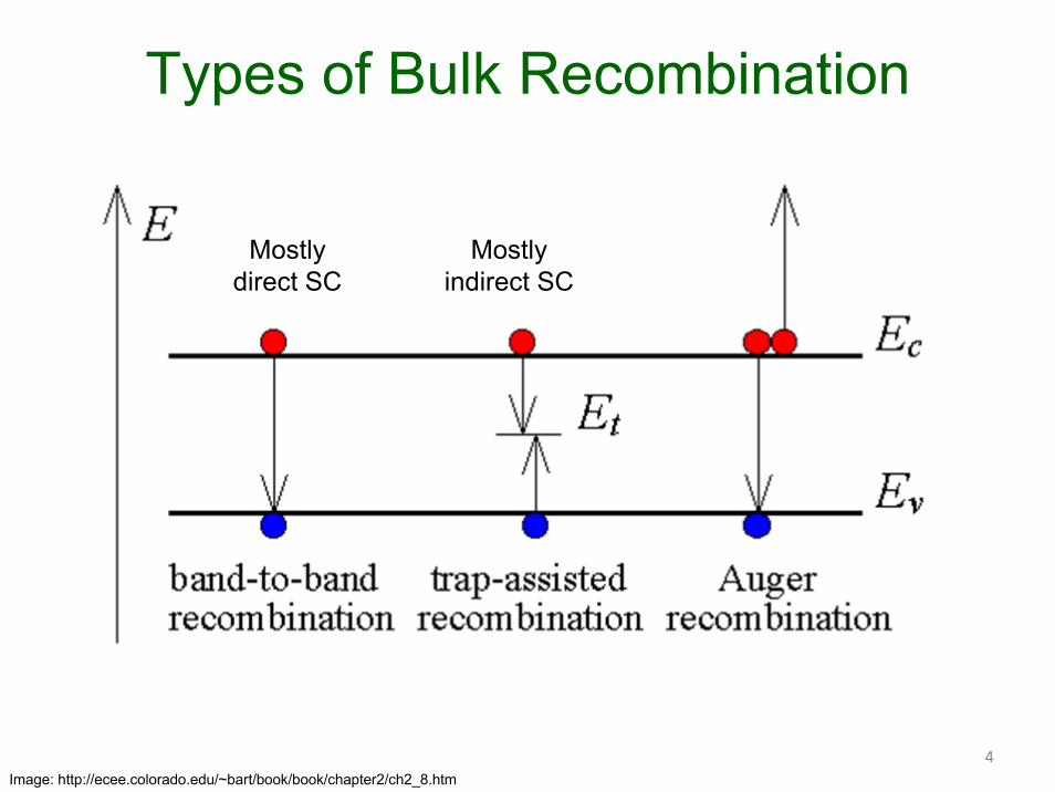
4
Types of Bulk Recombination
Image: http://ecee.colorado.edu/~bart/book/book/chapter2/ch2_8.htm
Mostly direct SC
Mostly indirect SC

5
A Characteristic Current-Voltage Curve for a Photovoltaic Cells
6
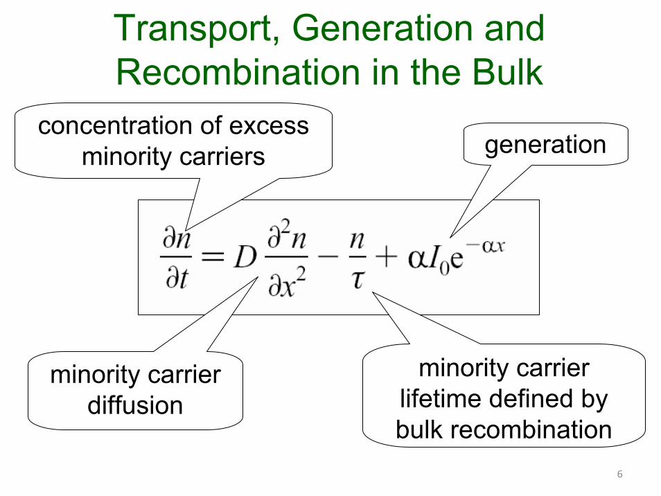
Transport, Generation and Recombination in the Bulk
generationconcentration of excess
minority carriers
minority carrier lifetime defined by bulk recombination
minority carrier diffusion
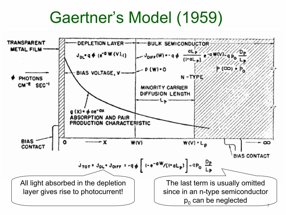
7
Gaertner’s Model (1959)
The last term is usually omitted since in an n-type semiconductor
p0 can be neglected
All light absorbed in the depletion layer gives rise to photocurrent!

8
Gaertner’s Model
∫ −Φ== −W
WDL eqdxxgqJ
0
)1()( α
All light absorbed in the depletion layer gives rise to photocurrent! No recombination!
xexg ⋅−Φ⋅= αα)(

9
Gaertner’s Model
Furthermore, if α-1<<W (weakly absorbed light), then
If further Lp<<W (high recombination in the quasi-neutral region or low mobility), then p
p
pphoto
LWL
q
WL
qj
αα
αα
++
Φ−=
=−+
−Φ−=
1
))1(1
11(
Wqjphoto Φ−= α
The photocurrent is proportional to the width of the space-charge layer!

10
Gaertner’s Model
Wqjphoto ⋅Φ⋅⋅−= α
The photocurrent is proportional to the square root of the bias applied across the space-charge region and will also increase with a decrease in the donor density (wider SCR).
Gaetner’s model does not account for recombination in the SCR and at the interface! The only factor is the minority carrier diffusion length Lp.
fbDNe
W φφεε −=0
02

11
Wilson’s Model (1977)
S is the kinetic parameter related to the rates of surface reactions,
recombination and charge transfer
tr SSS +=

12
Wilson’s Model
⎟⎟⎠
⎞⎜⎜⎝
⎛++
−+−−+
Φ−=1/
)exp()exp(1p
p
p
p
rt
tphoto L
LSDL
LWW
SSSqj
αα
αα
cf. (Gaertner’s model):
⎟⎟⎠
⎞⎜⎜⎝
⎛+
−−Φ−=1
1)exp(1p
photo LWqj
αα

13
Wilson’s Model

14
Surface recombination suppressed
Experimental effect of surface recombination
Semenikhin et al Langmuir 15, 1999, 3731
15
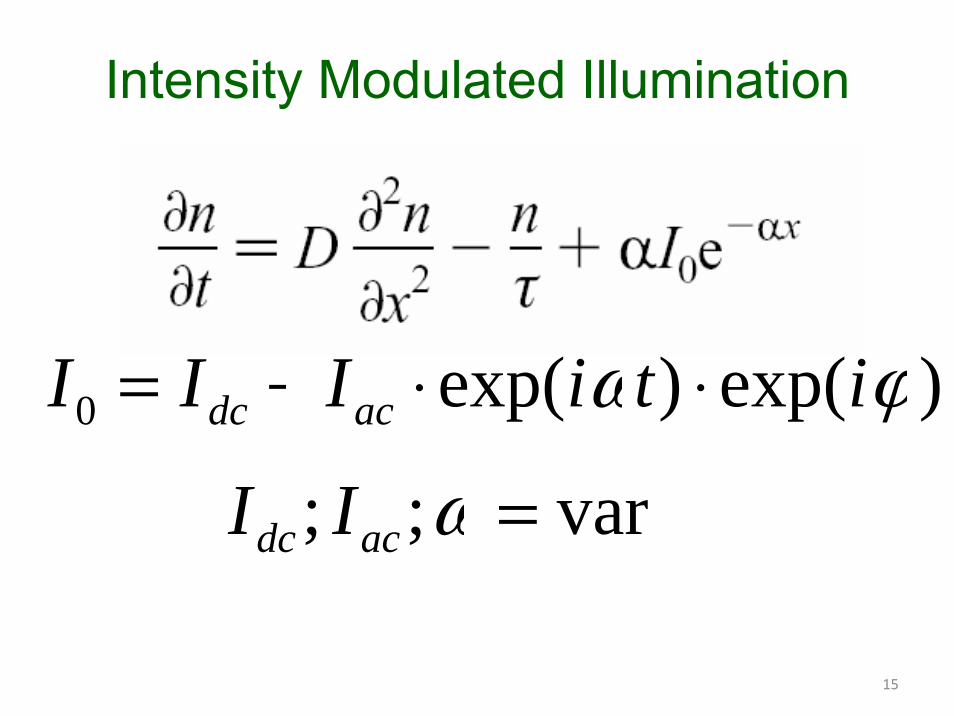
Intensity Modulated Illumination
)exp()exp(0 ϕω itiIII acdc ⋅⋅+=
var;; =ωacdc II

16
Intensity Modulated Photocurrent/ Photovoltage Spectroscopy (IMPS/IMVS)
– sinusoidal modulation of the laser light intensity• MHz mHz
• 10 ns 100 s
– the modulation depth can be varied allows studies of non‐linear behaviour
– ac photocurrent and ac photovoltage measured using a Frequency Response Analyzer (FRA)
– the frequency dependencies are presented on the complex plane (Nyquist plots) and as Bode plots of the photocurrent magnitude and phase vs. frequency.

17
IMPS Background
φ = 0, photocurrent is in phasewith the light intensity Mag
Imag
inar
y P
hoto
curr
ent
Real Photocurrent
III
III IV
Am
plitu
de
t
Phot
ocur
rent
0 t
Light IntensityPhotocurrent Magnitude
Light Off
Light On

18
IMPS Background
Positive φ, photocurrentleads the intensity
Am
plitu
dePh
otoc
urre
nt
0 t
φ
Imag
inar
y P
hoto
curr
ent
Real Photocurrent
III
III IV
t
Light IntensityPhotocurrent Magnitude
Light Off
Light On

19
IMPS BackgroundPh
otoc
urre
nt
0 t
Negative φ, photocurrent lags behind the intensity
Am
plitu
de
φ
Imag
inar
y P
hoto
curr
ent
Real Photocurrent
III
III IV
t
Light IntensityPhotocurrent Magnitude
Light Off
Light On
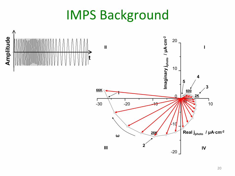
20
IMPS Background
-30 -20 -10 10
-20
-10
0
10
20
Real jphoto / μA·cm-2
Imag
inar
y j p
hoto
/ μA
·cm
-2
III
III IV
ω
1
2
3
45
66K
26K
40
6002K
Am
plitu
de
t
21
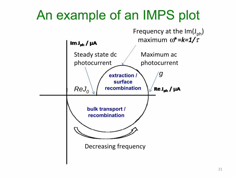
An example of an IMPS plot
Steady state dc photocurrent
Maximum ac photocurrent
Decreasing frequency
ReJ0
g
bulk transport / recombination
extraction / surface
recombination
Frequency at the Im(Jph) maximum ω*=k=1/τ
22
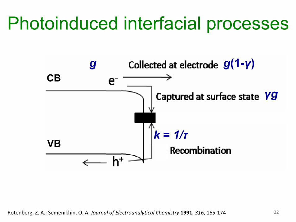
Photoinduced interfacial processes
22Rotenberg, Z. A.; Semenikhin, O. A. Journal of Electroanalytical Chemistry 1991, 316, 165‐174
g(1-γ)
γg
k = 1/τ
CB
VB
g

23
Intensity Modulated Illumination: Surface Processes
kpgdtdp −= γ
)exp();exp();exp(
tiggtipptiII
ωωω
⋅=⋅=⋅=
)1(; pkgjik
gp
kpgpi
photo ⋅−⋅=+
=
−=
ωγγω

24
Intensity Modulated Illumination: Surface Processes
)1()1(ω
γikkgpkgjphoto +
⋅−=⋅−⋅=

25
Intensity Modulated Illumination: Surface Processes

26
Intensity Modulated Illumination: Surface Processes
τω /1* == k

27
Intensity Modulated Illumination: Bulk Processes
Dloczik et al J. Phys. Chem. B 1997, 101, 10281-10289
28

29
steady state periodic illumination
IMPS response

30Dloczik et al J. Phys. Chem. B 1997, 101, 10281-10289
IMPS of bulk diffusion/recombination in dye‐sensitized solar cells
Diffusion-limited case: kext >> γ D (fast extraction):

31Dloczik et al J. Phys. Chem. B 1997, 101, 10281-10289
IMPS of bulk diffusion/recombination in dye‐sensitized solar cells
theory experiment
The electrode potential changes the interfacial rate constant of carrier extraction

32
An example of an IMPS plot
Steady state dc photocurrent
Maximum ac photocurrent
Decreasing frequency
ReJ0
g
bulk transport / recombination
extraction / surface
recombination
Frequency at the Im(Jph) maximum ω*=k=1/τ

33
IMPS studies of non-linear systemsI(ω) = Idc + Iacsin(ωt)
jphoto(ω) = jphoto dc + jphoto acsin(ωt+φ)Idc= var, Iac= const
jphoto,ac= f(ω,Idc)
This system is non-linear! The IMPS traces and parameters of the photoprocess change with the dc light intensity. A linear system would exhibit the same trace for all intensities.

34
The Time-of-Flight Portion
Time-of-flight portion
The TOF portion appears at high modulation frequencies with cells illuminated with strongly absorbed light from the back contact. The packets of carriers reach the top contact after a TOF delay, which is translated in the frequency domain into a spiral loop at high frequencies.

35
Organic Donor-Acceptor Solar Cells
36
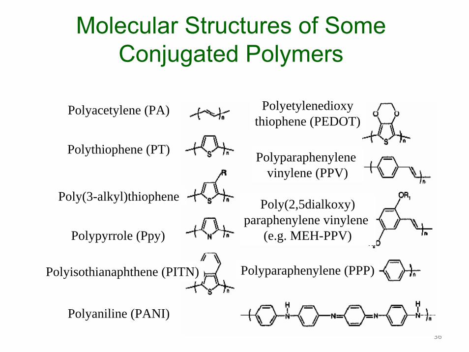
Molecular Structures of Some Conjugated Polymers
Polyacetylene (PA)
Polythiophene (PT)
Poly(3-alkyl)thiophene
Polypyrrole (Ppy)
Polyisothianaphthene (PITN)
Polyaniline (PANI)
Polyetylenedioxythiophene (PEDOT)
Polyparaphenylene vinylene (PPV)
Poly(2,5dialkoxy)paraphenylene vinylene
(e.g. MEH-PPV)
Polyparaphenylene (PPP)
37
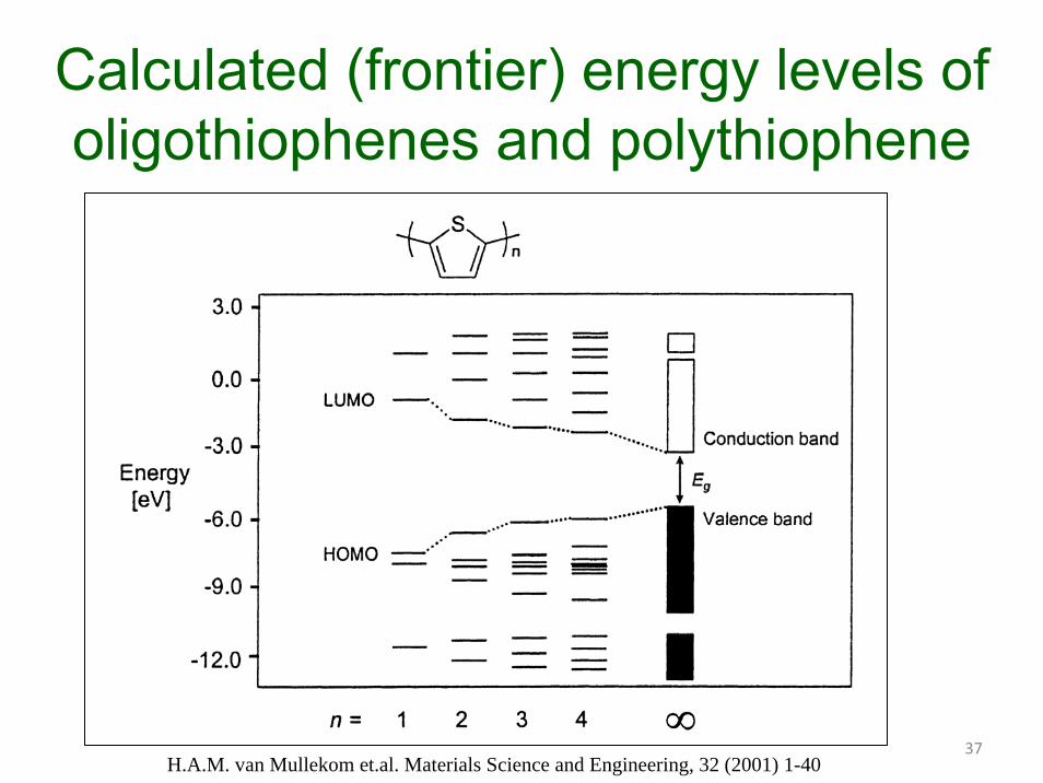
Calculated (frontier) energy levels of oligothiophenes and polythiophene
H.A.M. van Mullekom et.al. Materials Science and Engineering, 32 (2001) 1-40

38
Photovoltaics and Photoconductivity in Organic Molecular Solids
• Organic molecular solids are semiconductors with wide wide band gapsband gaps and narrow bandsnarrow bands.
• This is due to the fact that the overlapping overlapping ππ--orbitalsorbitalsbelong to different moleculesdifferent molecules and overlapping is necessarily rather weakweak.
•• Narrow bandsNarrow bands mean relatively low conductivitylow conductivity. In other terms, the effective masseseffective masses of carriers in molecular solids are highhigh.
• The main uses of semiconductors are in electronics and in various photovoltaic/photoconductive/luminescent devices.
• Narrow bands and low mobilities do not favour the use of these materials in electronics. However, wide bandgaps and low dark conductivities are perfect for various photo-related technologies.

39
Photovoltaics and Photoconductivity in Organic Molecular Solids (cont-d)
• Photoconduction in organic molecular solids (anthracene) was discovered as early as in 1906, at the same time as that of Si.
• A prototype of an organic photovoltaic cell was made by the father of electrochemical kinetics Max Vollmer in 1913.
• All these photo-related phenomena are based on generation of mobile charge carriers upon absorption of light by an organic material.
• The light should possess a certain threshold energy. This energy is related but not always equal to the band gap.
• Photoconductivity is carrier movement in external electric field.• The difference between photoconductivity and photovoltaic
effect is that in the latter case photoexcited carriers can alsocreate an internal electric field.

40
Photoexcitation in organic materials. Excitons vs. free electrons and holes.
• What are the elementary photoexcitations responsible for photoconductivity and other related properties?
• We have heard many times that in inorganic semiconductors such as Si, the photogenerated charge carriers are free electrons and holes. But what does the term “free” means?
• In fact, elementary photoexcitations in organic materials and also in many cases in inorganic semiconductors are so-called excitons rather than free electrons and holes.
• An exciton is an electron and a hole bound together by Coulombic attraction that lowers their energy. This energy difference between free and bound e-h pairs is called the exciton binding energy.
• The difference between excitons and elementary excited states is that excitons are moving excited states ☺ Their lifetime is long enough to move inside the material.

41
Photoexcitation in organic materials. Excitons vs. free electrons and holes.
• Well, how about free electrons and holes? Was that model absolutely wrong? Since an electron is always negative and a hole is always positive, there will always be some Coulombic interaction between them and they should always be bound in excitons, right?
• Well, yes, to a point, but in many practical cases this binding energy is as small as a few meV and insignificant as compared to the thermal motion energy kBT.
• If a material has many charge carriers and many charges, these charges efficiently screen the Coulombic interaction and the exciton binding energies are small. This is the case with inorganic semiconductors.
• If a material has a few charges, the screening is not efficient and excitons have large binding energies. This is the case with molecular crystals.

42
Excitons in Molecular Crystals
The electron-hole binding energy with
applied external electric field
The energy of Coulombicinteraction between an
electron and a hole. Further separation decreases this
energy. The electron energy level becomes
higher (less favourable).
43
• As can be inferred from the above, there are various degrees of delocalization between photoexcited electrons and holes. As dependent on the delocalization, several types of excitons can be defined.
• The first case, photoexcited electron and hole on the same molecule, is called a Frenkel exciton. It is the most localized excitation with the radius similar to the size of a molecule and smaller than the intermolecular distance. It is neutral and moves by diffusion. Usually, its lifetime is very short, although it can be longer in luminescent materials.
• The second case corresponds to the most delocalized Wannier-Mott exciton. Due to very efficient screening (many charge carriers or efficient orbital overlapping resulting in high polarizability), the exciton radius is very large, many times the size of the lattice constant. This exciton can be readily dissociated, e.g., by electric field.
Excitons in Molecular Crystals

44
Excitons in Molecular Crystals

45
• At intermediate delocalizations, we have charge-transfer (CT) excitons. They are neither very extended nor tightly bound to a single molecular site.
• However, additional localization can occur if the charge-lattice interaction (sometimes given by periodic lattice pseudo-potential Vpseudo) is strong.
• In covalently bound solids, the correlation between excited electronic states is strong because of efficient overlap of neighbouring molecular orbitals (relatively wide bands). This weakens the interaction of charges with the lattice. The charge density is delocalized but the delocalization is less than in the case of Wannier-Mott excitons.
• In weakly bonded molecular crystals, the overlap is small (narrow bands). The variations in the electron energy due to Vpseudo are larger than the band width. Extended bands may cease to exist. Carriers are localizes on individual molecules.
Excitons in Molecular Crystals

46
Excitons in Molecular Crystals
Vpseude is the periodic pseudopotential of
the lattice
47
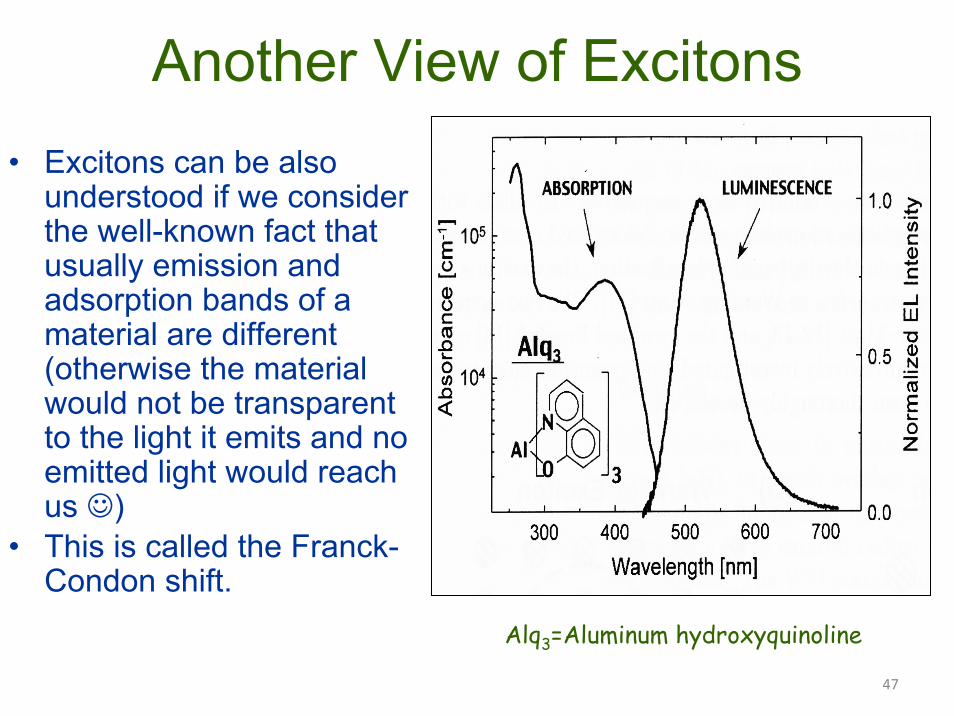
• Excitons can be also understood if we consider the well-known fact that usually emission and adsorption bands of a material are different (otherwise the material would not be transparent to the light it emits and no emitted light would reach us ☺)
• This is called the Franck-Condon shift.
Another View of Excitons
Alq3=Aluminum hydroxyquinoline

48
• The Franck-Condon shift is due to rearrangement of the lattice because the excited-state geometry differs from that of the ground state.
• This is the result of charge-lattice interaction, the same that brought about excitons.
• In chemical terms, exciton formation is a change in molecular geometry.
• The greater the required change in geometry, the more localized is the exciton and the higher is its binding energy.
Another View of Excitons

49
Excitons and Photogeneration• Well, as we have seen, in some materials photoexcitation
results in formation of various types of excitons.• However, excitons are neutral and cannot carry charge so that
no energy can be collected.• To ensure photogeneration of energy, excitons must be
separated to produce electron-hole pairs.• This process require overcoming of the exciton binding energy
(usually, by external electric field).• A competing process is recombination (relaxation of
photoexcited electrons back to the ground state). The excess energy is either dissipated into lattice vibrations (non-radiativerecombination) or emitted as light (radiative recombination).
• Tightly bound excitons are hard to separate =>poor photogeneration.
• If exciton lifetime is very short (high recombination rate) theycannot be separated and again we have poor photogeneration.

50
Organic Donor-Acceptor Photovoltaic Cells

51
Organic Donor-Acceptor Photovoltaic Cells

52
Organic Photovoltaic Cells
PQT
PCBM = phenyl-C61-butyric acid methyl ester

53
Bulk Heterojunction Organic Photovoltaic Cells

54
Photovoltaic Device Structure
54Steim, R.; Kogler, F. R.; Brabec, C. J. Journal of Materials Chemistry 2010, 20, 2499‐2512

55
Donor‐Acceptor Effect and Exciton Dissociation
55Steim, R.; Kogler, F. R.; Brabec, C. J. Journal of Materials Chemistry 2010, 20, 2499‐2512

56
Charge Transport through Percolation Pathways
56Steim, R.; Kogler, F. R.; Brabec, C. J. Journal of Materials Chemistry 2010, 20, 2499‐2512

57
Carrier Transport, Extractionand Recombination
• The efficiency of a solar cell is largely determined not only by the primary exciton dissociation but also by the transport in the photoactive material and the processes at the interfaces, as well as recombination losses both in the bulk and at the interfaces.
• The carriers must be extracted efficiently; otherwise, the efficiency of even a very good material will be low.
• The efficiency of the transport and extraction of carriers depends on many factors. They can be studied by using IMPS and IMVS.

58
IMPS plots without acceptor moiety
-30 -20 -10 10
-20
-10
0
10
20
Real jphoto / μA·cm-2
Imag
inar
y j ph
oto
/ μA
·cm
-2
III
III IV
ω
1
2
3
45
66K
26K
40
6002K
CathodicAnodic
ITO/PEDOT/PBT/Albias = 0.0 V
Anodic
Cathodic
59
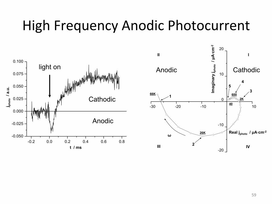
High Frequency Anodic Photocurrent
-30 -20 -10 10
-20
-10
0
10
20
Real jphoto / μA·cm-2
Imag
inar
y j p
hoto
/ μA
·cm
-2
III
III IV
ω
1
2
3
45
66K
26K
40
6002KCathodic
Anodic
-0.2 0.0 0.2 0.4 0.6 0.8
CathodicAnodic
-0.050
-0.025
0.000
0.025
0.050
0.075
0.100
t / ms
j pho
to/ a
.u.
light on

60
Not only excitons are poorly dissociated, but also:
• Holes move in wrong direction (to the Al cathode).– Trapped at electrode.
• Electrons flow to cathode at lower ω.– Recombine with holes.
-30 -20 -10 10
-20
-10
0
10
20
Real jphoto / μA·cm-2
Imag
inar
y j p
hoto
/ μA
·cm
-2
III
III IV
ω
1
2
3
45
66K
26K
40
6002K
VB
Fermi-Level
Fermi-Level
h+
e-
ActiveLayer
CB
CathodeAnode0
1
3
2
4
5
6
Ene
rgy
/ eV
(Al)(ITO)
IMPS plots without acceptor moiety

61
IMPS studies of “standard”ITO/PEDOT/P3HT:PCBM/AlDonor-Acceptor Solar Cells
See also: J. C. Byers, S. Ballantyne, K. Rodionov, A. Mann, and O. A. Semenikhin. Mechanism of Recombination Losses in Bulk Heterojunction P3HT:PCBM Solar Cells Studied Using Intensity Modulated Photocurrent Spectroscopy. ACS Advanced Materials and Interfaces, 2011, vol. 3, pp.392-401
62
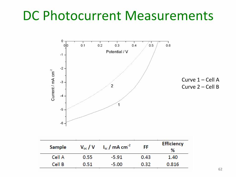
DC Photocurrent Measurements
62
Curve 1 – Cell ACurve 2 – Cell B

63
IMPS spectra ‐ Efficient and Less Efficient Cells
Plot 1 – Cell APlot 2 – Cell B
Photon intensity of 8.18x10¹⁵ s‐1cm‐2
Less efficient Cell B shows larger surface recombination
63

64
IMPS spectra – Effect of ageing
64
Plot 1 – Cell B after fabricationPlot 2 – Cell B two months later
Photon intensity of 8.18x10¹⁵ s‐1cm‐2
The dc photocurrent is zero after ageing; however, there is still an ac photocurrent. IMPS shows that surface recombination is a
major reason of the deterioration of the aged cells performance!

65
The Effect of dc Bias
•IMPS spectra taken at bias values ranging from 0.0 V (short-circuit) to +0.5 (near open-circuit) show that the generation current decreases and the surface recombination rate increases near the open-circuit conditions. •This is one of the reason for reduced fill factor and lower efficiency.
0.1 0.2 0.3 0.4 0.5 0.6
-0.15
-0.10
-0.05
0.00
0.05
0.10
0.15
Im(J
) / m
A c
m2
Re(J) / mA cm2
ω∗1
23
1 - +0.0 V; 2 - + 0.25 V; 3 - +0.5 V

66
The Effect of dc Light Intensity
•The ac photocurrent decreases with the dc light intensity. The system is non-linear! •The frequency at the maximum of the imaginary component ω*, which corresponds to the surface recombination rate, increases with the dc light intensity. •This means that electrons recombine in part with photogenerated holes trapped at the interface.
ω∗
-0.3 0.0 0.3 0.6 0.9 1.2 1.5
-0.6
-0.3
0.0
0.3
Im(J
) / m
A c
m-2
Re(J) / mA cm-2
123
45
The dc intensity increases 1→5

67
IMVS: charge transport and accumulation at open circuit
The dc intensity increases 1→5
•The IMVS also shows that the system is non-linear. •The frequency at the maximum of the imaginary component ω* increases with the dc light intensity. This again suggests that the lifetime of the carriers decreases with an increase in the lightintensity due to surface and the bulk recombination. The mathematical model of the bulk photoprocesses is needed to separate these from the surface recombination.

68
-0.2 -0.1 0.0 0.1 0.2 0.3 0.4 0.50.00E+000
4.00E+013
8.00E+013
1.20E+014
1.60E+014
Bias / V
C-2 /
F-2 c
m4
-0.2 0.0 0.2 0.4 0.6 0.80.0
2.0x10¹²
4.0x10¹²
6.0x10¹²
8.0x10¹²
1.0x10¹³
1.2x10¹³
1.4x10¹³
C-2 /
F-2 c
m4
Bias / V
Mott‐Schottky plots indicate photoinduced hole trapping
Evidence of Fermi-level pinning, indicates the
presence of surface states

69
The trap densities from Mott‐Schottky plots at various dc light intensities…
0 1x10¹⁶ 2x10¹⁶ 3x10¹⁶ 4x10¹⁶ 5x10¹⁶ 6x10¹⁶ 7x10¹⁶
0.0
2.0x10¹⁶
4.0x10¹⁶
6.0x10¹⁶
8.0x10¹⁶
1.0x10¹⁷
1.2x10¹⁷
ND /
cm-3
Intensity / s-1 cm-2
fresh cell
aged cell

70
…and the values of the recombination rate constant from IMPS plots…
0 1x10¹⁶ 2x10¹⁶ 3x10¹⁶ 4x10¹⁶ 5x10¹⁶ 6x10¹⁶ 7x10¹⁶
0.0
5.0x10³
1.0x10⁴
1.5x10⁴
2.0x10⁴
2.5x10⁴
3.0x10⁴
3.5x10⁴
4.0x10⁴k
/ s-1
Intensity / s-1 cm-2
fresh cell
aged cell

71
The recombination of electrons in the acceptor layer is in part related to photogenerated holes
trapped in the photovoltaic layer!
0.0 2.0x10¹⁶ 4.0x10¹⁶ 6.0x10¹⁶ 8.0x10¹⁶ 1.0x10¹⁷ 1.2x10170.0
5.0x10³
1.0x10⁴
1.5x10⁴
2.0x10⁴
2.5x10⁴
3.0x10⁴
3.5x10⁴
k / s
-1
ND / cm-3
72
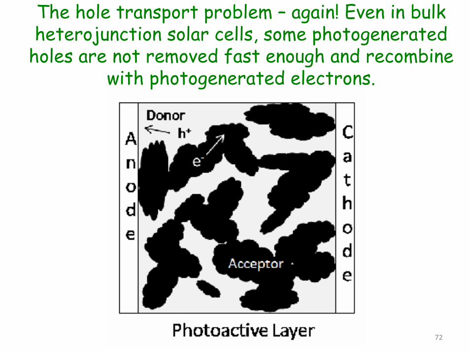
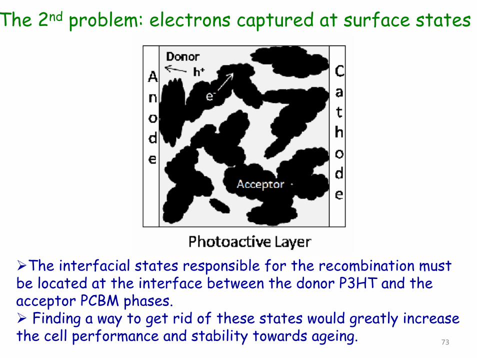
The hole transport problem – again! Even in bulk heterojunction solar cells, some photogenerated
holes are not removed fast enough and recombine with photogenerated electrons.
73
The interfacial states responsible for the recombination must be located at the interface between the donor P3HT and the acceptor PCBM phases.
Finding a way to get rid of these states would greatly increasethe cell performance and stability towards ageing.
The 2nd problem: electrons captured at surface states
74
Conclusions• The use of IMPS/IMVS allows one to clearly separate
the bulk and interfacial recombination processes in solar cells. Additionally, carrier transport may be characterised too (mobilities, trapping…).
• 2. The light intensity dependence can be studied with great precision by applying quazi-linear conditions (dc+ac light intensity).
• 3. The analysis is performed under normal working conditions of a solar cell, just using modulated illumination. This makes it easier to relate the results of the IMPS experiments to regular steady-state photocurrent / efficiency measurements, unlike many other transient techniques.

75
Students• Josh Byers
DiscoveryEngage
Industrial Partner
Collaborations•Thomas Heiser, Institut d'Électronique du Solide et des Systèmes (InESS), University of Strabsourg
Financial Support

76
London, Ontario, Canada

77
The University of Western Ontario

78
Our Department