terahertz transport dynamics of graphene charge...
TRANSCRIPT
General rights Copyright and moral rights for the publications made accessible in the public portal are retained by the authors and/or other copyright owners and it is a condition of accessing publications that users recognise and abide by the legal requirements associated with these rights.
• Users may download and print one copy of any publication from the public portal for the purpose of private study or research. • You may not further distribute the material or use it for any profit-making activity or commercial gain • You may freely distribute the URL identifying the publication in the public portal
If you believe that this document breaches copyright please contact us providing details, and we will remove access to the work immediately and investigate your claim.
Downloaded from orbit.dtu.dk on: May 20, 2018
Terahertz transport dynamics of graphene charge carriers
Buron, Jonas Christian Due; Jepsen, Peter Uhd; Bøggild, Peter
Publication date:2013
Document VersionPublisher's PDF, also known as Version of record
Link back to DTU Orbit
Citation (APA):Buron, J. C. D., Jepsen, P. U., & Bøggild, P. (2013). Terahertz transport dynamics of graphene charge carriers.Kgs. Lyngby: Technical University of Denmark (DTU).
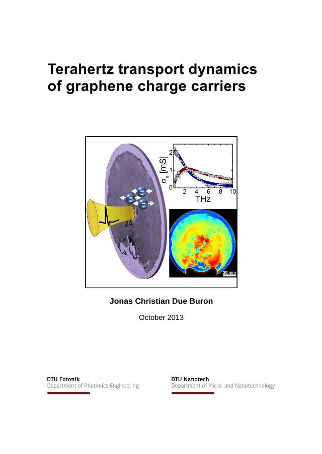
Terahertz transport dynamics of graphene charge carriers
Jonas Christian Due Buron
October 2013

i
Abstract
The electronic transport dynamics of graphene charge carriers at
femtosecond (10-15
s) to picosecond ( 1210 s ) time scales are investigated
using terahertz ( 1210 Hz ) time-domain spectroscopy (THz-TDS). The
technique uses sub-picosecond pulses of electromagnetic radiation to gauge
the electrodynamic response of thin conducting films at up to multi-terahertz
frequencies. In this thesis THz-TDS is applied towards two main goals; (1)
investigation of the fundamental carrier transport dynamics in graphene at
femtosecond to picosecond timescales and (2) application of terahertz time-
domain spectroscopy to rapid and non-contact electrical characterization of
large-area graphene, relevant for industrial integration.
We show that THz-TDS is an accurate and reliable probe of graphene sheet
conductance, and that the technique provides insight into fundamental
aspects of the nanoscopic nature of conduction in graphene films. This is
demonstrated by experimental observation of diffusive transport as well as
signatures of preferential back-scattering of carriers on a nanoscopic scale in
poly-crystalline graphene, which may be related to reflections at crystal
domain boundaries. This is the first observation of preferential back-
scattering of graphene charge carriers in THz-TDS measurements, and the
results are expected to have a significant impact on the graphene and THz-
TDS communities, as they may provide insight into the impact of
nanoscopic morphology on the electrical conduction in poly-crystalline
graphene. Through THz-TDS measurements with accurate carrier density
control by careful electrical back-gating, we find that terahertz conductance
scales linearly with carrier density, consistent with charge transport limited
by long-range scattering on charged impurities, which is also observed in
most contact-based transport measurements.
By demonstrations of wafer-scale sheet conductance mapping and large-area
field-effect mobility mapping, it is shown that the non-contact nature of
THz-TDS measurements facilitates the rapid and reliable large-scale
characterization of graphene electronic properties and their uniformity, that
might be viewed as a vital requirement for industrial implementation of the
material. We find significant spatial variations in carrier mobility of a factor
of 2-3 on a scale of just few millimeters, which highlights the importance of
techniques that provide highly statistical or spatially resolved approaches to
electronic characterization of large-area graphene. In a comparative study,
ii
we observe significant suppression of DC micrometer-scale transport,
probed using micro four-point probe conductance mapping, relative to AC
nanoscopic transport, probed by THz-TDS conductance mapping. A detailed
analysis of micro four-point probe, THz-TDS and Raman spectroscopy data
reveals that the suppression of micrometer-scale conductance is a signature
of electrical defects on the scale of 10 m, giving rise to 1D-like
micrometer-scale transport.

iii

iv
v
Resume
Den elektroniske transport dynamic for graphene ladningsbærere på
femtosekund (10-15
s) til picosekund ( 1210 s ) tidsskala undersøges ved
hjælp af terahertz tids-domæne spektroskopi (THz-TDS). Teknikken, som
benytter sub-picosekund pulser af elektromagnetisk stråling til at måle det
elektrodynamiske respons for tynde, lendende film ved op til multi-THz
frekvenser, anvendes i denne afhandling med henblik på 2 primære mål; (1)
undersøgelse af fundamental dynamik i ladningsbærertransport for graphene
på femtosekund til picosekund tidsskalaer og (2) anvendelse af terahertz
tids-domæne spektroskopi til hurtig og kontaktfri elektrisk karakterisering af
stor-skala graphene, relevant for industrielle anvendelser.
Vi viser at THz-TDS giver et nøjagtigt og pålideligt mål for
fladekonduktansen af graphene såvel som fundamentale aspekter af den
elektriske ledningsproces i graphene. Dette demonstreres ved eksperimentel
observation af diffusiv ladningsransport og signaturer fra præferentiel
tilbagespredning af graphene ladningsbærere på nanoskopisk skala i
polykrystallinsk graphene, som kan være relateret til reflektioner ved
krystaldomænegrænser. Dette er den første observation af præferentiel
tilbagespredning af graphene ladningsbærere i THz-TDS målinger, og det
forventes at resultaterne vil have stor betydning indenfor graphene og THz-
TDS felterne, da de kan give indsigt i indflyselsen af nanoskopisk morfologi
på den elektriske ledningsevne i polykrystallinsk graphene. Ud fra THz-
TDS målinger med præcis control over ladningsbærertætheden ved hjælp af
nøje udført elektrisk forspænding, finder vi at terahertz konduktansen
skalerer lineært med ladningsbærertæthed, hvilket afspejler ladningstransport
begrænset af langdistance spredning af ladningsbærere på ladede urenheder,
som også observeres i de fleste kontakt-baserede transport målinger.
Ved demonstration af wafer-skala fladekonduktans-billeddannelse og stor-
skala felteffekt bevægeligheds-billeddannelse viser vi at den kontakt-fri
natur af THz-TDS målinger muliggør den hurtige og pålidelige stor-skala
karakterisering af graphene’s elektroniske egenskaber og deres uniformitet,
som kan anses for at være af afgørende nødvendighed for industriel
implementering af materialet. Vi finder betydelig rumlig variation i
ladningsbærerbevægeligheden på en faktor 2-3 over kun få millimeter,
hvilket understreger vigtigheden af teknikker der muliggør statistiske eller
rumligt opløste tilgange til elektronisk karakterisering af stor-skala graphene.
I en komparativ undersøgelse observerer vi signifikant reduktion af DC
vi
mikrometer-skala transport, udmålt ved hjælp af mikro-firpunkts-probe
konduktans kortlægning, i forhold til AC nanoskopisk transport, udmålt ved
hjælp af THz-TDS konduktans kortlægning. En detaljeret analyse af mikro-
firpunkts-probe-, THz-TDS- og Raman spektroskopi-data afslører at
reduktionen af mikrometer-skala ledningsevnen er et resultat af elektriske
defekter på en 10 m-skala, som giver anledning til 1D-lignende
mikrometer-skala transport.

vii

viii
ix
Preface
This Ph.D. thesis is the result of research conducted during my time as a
Ph.D. student at the technical University of Denmark (DTU) in the period
from August 1st 2010 to October 31
st 2013. The research was carried out
under supervision of professor Peter Uhd Jepsen, head of the Terahertz
Technologies and Biophotonics Group at DTU Fotonik, and associate
professor Peter Bøggild, head of the Nanocarbon Group at DTU Nanotech.
All terahertz time-domain spectroscopy results presented in the thesis were
obtained at DTU Fotonik, Department of Photonics engineering. Raman
spectroscopy measurements were performed at DTU Nanotech, Department
of Micro- and Nanotechnology. Silicon microfabrication was performed at
the cleanroom facility, DTU Danchip.
The micro four-point probe measurements presented in the thesis were
obtained by senior scientist Dirch Hjorth Petersen at DTU Nanotech and
Capres A/S. The CVD graphene samples presented in chapter 4 were
prepared by Ph.D. student Filippo Pizzocchero at DTU Nanotech, Ph.D.
student Eric Whiteway and associate professor Michael Hilke at McGill
University, Montreal, Quebec, Canada, and Alba Centeno and Dr. Amaia
Zurutuza at Graphenea S.A., Donostia-San Sebastian, Spain. The CVD
graphene samples presented in chapter 5 were prepared by assistant
professor Jie Sun at the Quantum Device Physics Laboratory, Chalmers
University of Technology, Gothenburg, Sweden. The CVD graphene
samples presented in chapter 6 were prepared by Ph.D. student Filippo
Pizzocchero at DTU Nanotech.
This Ph.D. project was partially financed by DTU Fotonik (2/3) and DTU
Nanotech (1/3). I have received financial support for an external research
stay in Kyoto, Japan from Valdemar Selmer Tranes Fond, Augustinus
Fonden and Otto Mønsteds Fond. Financial support was given for laboratory
equipment and travel expenses by Augustinus Fonden, Oticon Fonden and
Taumoses Fond.
Jonas Christian Due Buron
Kongens Lyngby, October 31st 2013

x
xi
Acknowledgements
There is a long list of people that I am grateful to have had the pleasure of
knowing and working with during my Ph.D. project, without whom it is
likely that this thesis would never have come to be.
I would first of all like to thank my two supervisors, Prof. Peter Uhd Jepsen
and Prof. Peter Bøggild, for their supervision and guidance throughout the
past 5 years. I am extremely grateful to have been introduced to the world of
academic research by two people who, each in their own way, wield a
contagious passion and fervor for everything they undertake in their
research, and yet equally appreciate the importance of unwinding with
aspects of life not related to scientific endeavors. Not rarely in the vicinity of
a bar counter. I am certain that I would not have found myself in academia
today, had I not crossed paths with supervisors that I appreciate and relate to
on a personal level as much as Peter and Peter.
I am very thankful to Dr. David Cooke, who has been a true inspiration for
me and who shaped me and my research in graphene terahertz dynamics
from the first encounter in an under-graduate course at DTU. He is a
remarkable experimentalist and scientist who showed me the ropes in an
optics lab, and always challenged me with inspiring views and discussions in
the lab. I hope his lab stool still manages to make appearances in the
terahertz labs at McGill University.
I want to thank Dr. Dirch Hjorth Petersen, who has been a source of constant
frustration in the best possible way. As long as I have known Dirch he has
kept me on my toes, by exerting his god-given talent for, most often
completely justified, scrutinizing the validity of scientific results. Always
with a good sense of humor. There is no doubt i have benefited greatly both
scientifically and personally from knowing and working with Dirch.
I have been lucky to work closely with fellow Ph.D. student Filippo
Pizzocchero, whose productivity in our collaborations was only surpassed by
his flair for physics. Thanks for the always interesting collaborations and
discussions. I hope there are a lot more to come.
Though I cannot mention everyone by name, I want to express my thanks to
all current and former members of the Terahertz Technologies Group and
Nanocarbon Goup for an always inspiring and very enjoyable environment.
A special thank you to Dr. Maksim Zalkovskij for fruitful advice and
xii
discussions. He was an office mate, lab mate, travel mate, and a good friend
throughout the entire project. Also a thank you to fellow Ph.D. student
Pernille Klarskov Pedersen for many hours of distractions.
Finally, I want to thank my family and friends for always supporting and
helping me, and my friends in Grupo Ginga for always providing a perfect
escape from an at times stressful Ph.D. project.

xiii

xiv
xv
List of acronyms
1D – one-dimensional
2D – two-dimensional
2DEG – two-dimensional electron
gas
-Raman – micro-Raman
AC – alternating current
AlGaAs – aluminum gallium arsenide
Ar – argon
BHF – buffered hydrofluoric acid
CH4 – methane
Cu – copper
CVD – chemical vapor deposition
CNP – charge-neutrality-point
CW – continuous wave
DC – direct current
fs – femtosecond (10-15
s)
FTIR – fourier transform infrared
spectroscopy
FWHM – full width at half maximum
GaAs – gallium arsenide
GHz – gigahertz (109 Hz)
HEMT – high electron mobility
transistor
HR-Si – high resistivity silicon
HNO3 – nitric acid
InGaAs – indium gallium arsenide
InP – indium phosphide
ITO – indium tin oxide
LED – light emitting diode
LT-GaAs – low temperature.-grown
gallium arsenide
LT-InGaAs – low temperature-grown
indium gallium arsenide
M4PP – micro four-point probe
MBE – molecular beam epitaxy
MC – Monte Carlo
MOS – metal-oxide-semiconductor
(NH4)2S2O8 – ammonium persulfate
Nd:YLF – neodymium-doped yttrium
lithium fluoride
nm – nanometer (10-9
m)
PCS – photoconductive switch
PECVD – plasma-enhanced chemical
vapour deposition
PMMA – polymethyl-methacrylate
Poly-C – poly-crystalline
Poly-Si – poly-crystalline silicon
ps – picosecond (10-12
s)
QHE – quantum hall effect
r-GO – reduced graphene oxide
RD-SOS – radiation damaged silicon-
on-sapphire
xvi
RF – radio frequency
S-C – single-crystalline
sccm – standard cubic centimeter
SH – second harmonic
SHG – second harmonic generation
Si – silicon
SiC – silicon carbide
Si3N4 – silicon nitride
SiN – silicon nitride
SiO2 – silicon dioxide
THz – terahertz (1012
Hz)
THz-TDS – terahertz time-domain
spectroscopy
Ti:Sapphire – titanium-sapphire
UHV – ultra-high vacuum
Å – angstrom (10-10
m)
xvii
List of Figures
Figure 1.1: Transmittance and sheet resistance data for graphene films appearing in
the literature along with the industry standard defined by ITO. These are broken
down into films prepared by CVD, or from reduced graphene oxide or chemically
modified graphene, pristine exfoliated graphene, or chemically synthesized
graphene. The star represents the minimum industry requirement, corresponding to
DC/Op=35. The dashed line indicates all points corresponding to this ratio. The full
line corresponds to a calculated case of highly doped graphene layers. Reprinted5 .. 3
Figure 1.2: Complexity and feature sizes in integrated circuitry has followed Gordon
Moore statement from 1965, also known as‘Moore's law’, that transistor counts
would double every 18-24 months. Reprinted7 .......................................................... 4
Table 1: Carrier mobility for typical semiconducting materials. ................................ 5
Figure 1.3: Allotropes of hexagonal carbon. Schematic showing how the atomic
structure of graphene relates to other allotropes of hexagonal carbon. Reprinted15
... 5
Figure 2.1 : The hexagonal graphene crystal structure is constructed by a triangular
Bravais lattice with a two-atom structure within each unit cell, marked in dashed
line. On the right the corresponding Brillouin zone is shown. The band structure of
graphene can be calculated based on a tight-binding nearest-neighbor-hopping
approximation. The hopping potential between neighboring atoms is Vpp=-2.8 eV 11
Figure 2.2 : (a) Energy-momentum dispersion for graphene obtained from nearest-
neighbour tight-binding approximation in equation (2.4). Reprinted18
. (b) Band
diagram for graphene. Reprinted20
. .......................................................................... 13
Figure 2.3 : Raman spectra of pristine (top) and defected (bottom) graphene. The
main peaks are labelled. Reprinted23
. ....................................................................... 15
Figure 2.4 : (a) Schematic of the sample structure used in the initial work on electric
field effect in graphene films. (b) Sheet conductance as a function of back-gate
voltage for a micro-mechanically exfoliated monolayer graphene flake at T=10K.
The slopes reflect a field effect carrier mobility of around 15,000 cm2/Vs.
Reprinted2. (c) Hall measurements of carrier density and Hall mobility as a function
of back-gate voltage at T=1.7K. Reprinted3 ............................................................. 17
Figure 2.5 : Sheet carrier density calculated from the full expression in equation
(2.7) (red lines) and approximate expression where the quantum capacitance,
expressed in the second term on the right-hand-side is neglected (black lines), for (a)
5 Å SiO2 gate dielectric and (b) 50 nm SiO2 gate dielectric. .................................... 18
xviii
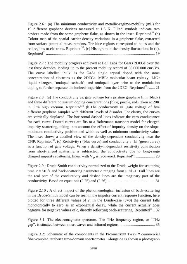
Figure 2.6 : (a) The minimum conductivity and metallic-regime-mobility (mL) for
19 different graphene devices measured at 1.6 K. Filled symbols indicate two
devices made from the same graphene flake, as shown in the inset. Reprinted32
(b)
Colour map of the spatial carrier density variations in a graphene flake, extracted
from surface potential measurements. The blue regions correspond to holes and the
red regions to electrons. Reprinted33
. (c) Histogram of the density fluctuations in (b).
Reprinted33
............................................................................................................... 19
Figure 2.7 : The mobility progress achieved at Bell Labs for GaAs 2DEGs over the
last three decades, leading up to the present mobility record of 36.000.000 cm2/Vs.
The curve labelled ‘bulk’ is for GaAs single crystal doped with the same
concentration of electrons as the 2DEGs. MBE: molecular-beam epitaxy; LN2:
liquid nitrogen; ‘undoped setback’: and undoped layer prior to the modulation
doping to further separate the ionized impurities from the 2DEG. Reprinted39
. ...... 21
Figure 2.8 : (a) The conductivity vs. gate voltage for a pristine graphene film (black)
and three different potassium doping concentrations (blue, purple, red) taken at 20K
in ultra high vacuum. Reprinted36
(b)The conductivity vs. gate voltage of five
different graphene samples with different levels of disorder. For clarity, the curves
are vertically displaced. The horizontal dashed lines indicate the zero conductance
for each curve. Dotted curves are fits to a Boltzmann transport model for charged
impurity scattering, taking into account the effect of impurity density on the slope,
minimum conductivity position and width as well as minimum conductivity value.
The inset shows a detailed view of the density-dependent conductivity near the
CNP. Reprinted32
. (c) Resistivity r (blue curve) and conductivity s=1/r (green curve)
as a function of gate voltage. When a density-independent resistivity contribution
from short-ranged scattering is subtracted, the conductivity due to long-range
charged impurity scattering, linear with Vg, is recovered. Reprinted21
. ................... 23
Figure 2.9 : Drude-Smith conductivity normalized to the Drude weight for scattering
time = 50 fs and back-scattering parameter c ranging from 0 til -1. Full lines are
the real part of the conductivity and dashed lines are the imaginary part of the
conductivity. Based on equations (2.25) and (2.26) ................................................. 31
Figure 2.10 : A direct impact of the phenomenological inclusion of back-scattering
in the Drude-Smith model can be seen in the impulse current response function, here
plotted for three different values of c. In the Drude-case (c=0) the current falls
monotonically to zero as an exponential decay, while the current actually goes
negative for negative values of c, directly reflecting back-scattering. Reprinted65
.. 32
Figure 3.1: The electromagnetic spectrum. The THz frequency region, or “THz
gap”, is situated between microwaves and infrared regions. .................................... 35
Figure 3.2: Schematic of the components in the Picometrix© T-ray™ commercial
fiber-coupled terahertz time-domain spectrometer. Alongside is shown a photograph
xix
of the THz spectrometer along with a laptop running the control software
(www.picometrix.com). ........................................................................................... 37
Figure 3.3: Schematic layout of traditional photoconductive switches. (a) Front view
of a PCS showing the metallic electrode and photoconductive gap forming the
Hertzian dipole antenna responsible for THz emission. (b) Side view showing the
HR-Si substrate lens used to collect and collimate the highly diverging THz
radiation emerging from the Hertzian dipole point-source. (c) Top view showing the
configurational scheme for THz generation in a PCS. (d) Top view showing the
conigurational scheme for THz detection in a PCS. ................................................ 38
Figure 3.4: Transient sheet photoconductivity of a detector system with c=500 fs,
s=30 fs and an optical pulse FWHM of 132.8 fs. (a) time-domain representation (b)
frequency-domain representation. The dashed line indicates the response function of
the detector when diffraction effects are included. Reprinted98
............................... 40
Figure 3.5: (a) Terahertz time-domain waveform recorded with the Picometrx© T-
ray™ 4000 system using 22mm thick aspheric poly-ethylene lenses with a working
distance of 25.4 mm. (b) Fourier transform of the THz transient in (a). .................. 41
Figure 3.6: (a) FWHM as a function of frequency for the Picometrix© T-ray™ 4000
system using aspheric poly-ethylene with a working distance of 25.4 mm. Data is
obtained by scanning the focused THz beam across the edge of a very straight and
highly uniform CVD graphene film. (b) THz image formation in the Picometrix© T-
ray™ 4000 is carried out by raster scanning the sample in the focal plane between
THz emitter and detector equipped with aspheric poly-ethylene lenses with working
distance of 25.4mm. Full THz time-domain waveforms are recorded in each pixel of
an image. .................................................................................................................. 42
Figure 3.7: Schematic of experimental setup for generation of free-space THz
transients from a two-color laser induced air plasma. .............................................. 44
Figure 3.8: Schematic of experimental setup for air-biased coherent detection of
THz transients. ......................................................................................................... 45
Figure 3.9: Schematic of experimental setup for ultra-broadband THz-TDS by two-
color plasma THz generation and air-biased coherent detection. ............................. 46
Figure 3.10: THz waveforms recorded in the THz air photonics spectrometer
provide bandwidth from 1 to up to 30 THz. (a) time-domain THz waveform
recorded with a temporal resolution of 10 fs. Inset shows the full temporal trace
from 0 to 3 ps (b) Fourier transform of the temporal waveform in (a) shows
bandwidth from approximately 1-30 THz ................................................................ 47
xx
Figure 3.11: Spitfire Pro Ti:Sapphire regenerative amplifier system from Spectra-
physics. Reprinted118
................................................................................................ 48
Figure 3.12: The THz response of the conducting thin film is isolated in the
complex-valued transmission function, Tfilm, as the sample Fourier transform divided
by the reference Fourier transform. .......................................................................... 50
Figure 3.13: The transmitted THz field are given by a combination of transmission,
reflection and propagation coefficients for each of the temporally separated echoes,
caused by multiple internal reflections. .................................................................... 51
Table 2: Transmission and reflection coefficients at normal incidence for boundaries
formed between air and a bulk, continuous medium. ............................................... 52
Figure 4.1: Monolayer graphene films exhibit an extraordinarily large THz response
due to an exceptionally high conductance. A single atomic layer of CVD graphene is
sufficient to reduce the amplitude of transmitted THz pulses by up to 20% as shown
for (a) time-domain, and (b) frequency-domain. ...................................................... 55
Figure 4.2: (a) Schematic of the sample structure. CVD graphene grown on single-
crystalline Cu (111), transferred to HR-Si wafer with 300 nm SiO2 layer. (b) Optical
microscopy image of the CVD graphene grown on single-crystalline Cu after
transfer onto oxidized HR-Si wafer. (c) Optical microscopy image of the CVD
graphene grown on poly-crystalline Cu after transfer onto oxidized HR-Si wafer.
Scale bars are 2 mm. ................................................................................................ 58
Figure 4.3: Sample and reference THz time-domain waveforms for CVD graphene
films grown on (a) single-crystalline Cu (111) substrate (b) poly-crystalline Cu foil.
Resulting sheet conductance spectra for (c) single-crystalline Cu (111) substrate (d)
poly-crystalline Cu foil. ........................................................................................... 59
Figure 4.4: Secondary electron micrograph of a micro four-point probe. Reprinted135
................................................................................................................................. 62
Figure 4.5: Illustration of the 3 independent configurations of contacts for current
injection and contacts for probing potential difference without presence of a
magnetic field. .......................................................................................................... 63
Figure 4.6: Example of the measurement outcome in a dual configuration M4PP
sheet resistance measurement. As indicated, the ratio between resistances obtained
in the A and B configurations is nominally 1.26 for an infinite, uniformly
conducting sheet. ...................................................................................................... 64
Figure 4.7: (a) Optical micrograph of the CVD graphene film grown on single-
crystalline Cu (111). The dashed line indicates the line along which the sheet
xxi
conductance was mapped by THz-TDS and dual configuration M4PP sheet
resistance line scan measurement. (b) M4PP and THz-TDS DC-extrapolated sheet
conductance as a function of position along the dashed line in (a). ......................... 65
Figure 4.8: (a) Sheet conductance measured by THz-TDS and M4PP with 4, 8, 12,
50, and 100 m probe pitch as a function of positions. (b) M4PP sheet conductance
for various probe pitches plotted against THz-TDS sheet conductance shows an
almost perfect 1:1 correlation. The full red line indicates a 1:1 correlation ............. 66
Figure 4.9: (a) Indications of the randomized M4PP sheet conductance measurement
locations on the poly-C Cu foil graphene film. (b) Correlation plot showing
measured M4PP sheet conductance as a function of measured THz-TDS sheet
conductance in the locations on the graphene films indicated in (a). The full red line
indicates a 1:1 correlation. ....................................................................................... 67
Figure 4.10: The substrate thickness of a 1mm thick HR-Si wafer was mapped with
100 m step size in an 11.4x11.4 mm2 area. The substrate thickness was obtained in
each pixel of the map by a fitting routine. On the right an example of the outcome of
one such fitting procedure is shown. ........................................................................ 69
Figure 4.11: Sample and reference THz time-domain waveforms for CVD graphene
films grown on (a) single-crystalline Cu (111) substrate (b) poly-crystalline Cu foil.
Resulting sheet conductance spectra for (c) single-crystalline Cu (111) substrate (d)
poly-crystalline Cu foil. ........................................................................................... 70
Figure 4.12: (a) Tiled optical microscopy image and (b) THz sheet conductance map
of CVD graphene film grown on single-crystalline Cu (111) substrate (average sheet
conductance in band from 0.9-1.0 THz). ................................................................. 74
Figure 4.13: (a) Optical microscopy image and (b) THz sheet conductance map of a
4 inch circular CVD graphene film grown on a high purity Cu film sputtered onto a
4 inch Si/SiO2 wafer. Transferred to HR-Si wafer by electrochemical transfer
technique. Average sheet conductance in band from 0.9-1.0 THz. (c) THz sheet
conductance map of a 6x4 cm2 CVD graphene film grown on Cu foil. Transferred to
HR-Si by sacrificial etching of Cu foil. Average sheet conductance in band from
0.9-1.0 THz. (graphene film is courtesy of Graphenea Inc.) (d) THz sheet
conductance map of a 4 inch circular CVD graphene film grown on Cu foil.
Transferred to HR-Si by sacrificial etching of Cu foil. Average sheet conductance in
band from 0.9-1.0 THz. (graphene film is courtesy of Graphenea Inc.) .................. 76
Figure 5.1: Combined THz-TDS, M4PP, Raman and optical mapping of large area
graphene on SiO2-on-Si substrate. Sketch depicting the principle of parallel
mapping of electrical conductance, Raman response and optical absorption on a
single-layer large area graphene film by THz-TDS, M4PP, -Raman and optical
microscopy. Bottom panel shows the relevant length scales of the physical processes
xxii
probed by each techniques. The combined information of these techniques facilitates
determination of electrical uniformity on nanometer and micrometer length scales
and correlation of electrical features to Raman and structural features. The sketch is
based on actual data maps. ....................................................................................... 81
Figure 5.2: Representative Raman spectra for the two investigated CVD graphene
samples. .................................................................................................................... 84
Figure 5.3: Example of THz-TDS time-domain data showing multiple echoes from
partial internal reflections in the SiO2-on-Si sample substrate. Sheet conductance
extraction is based on the Fourier transform (FFT amplitude shown in inset) of the
time-windowed 2nd transmitted pulse, E2 (indicated by gray shading), for areas with
(black line) and without (red line) graphene on the surface of the wafer. ................ 85
Figure 5.4: (a) Spectrally resolved sheet conductance of the two graphene films,
measured by THz-TDS. Characteristic length scales are based on an estimated
diffusion constant of D = 66 cm2/s. Triangles represent Re(s) and circles represent
Im(s). The spectra are obtained in the center of Figure 5.5(a) (sample 1, light grey)
and in the central conducting part of Figure 5.7(b) (sample 2, black). The full red
lines indicate the average real sheet conductances of the two samples, while the
dashed red lines indicates the zero-value of the negligible imaginary sheet
conductances of the two samples. The observed drop in THz sheet conductance at
the low end of the spectrum for sample 2 is caused by the low frequency parts of the
THz spot extending outside the area with uniform graphene coverage, as indicated in
the inset, and the small peak observed at 1.1 THz in Re(s) is an artifact caused by
the water vapour absorption line of ambient air. The indicated characteristic length
scale is discussed in the text. (b) Measured FWHM of the THz beam as a function of
frequency.................................................................................................................. 87
Figure 5.5: Images of homogeneous CVD grown graphene film on 90 nm SiO2 on
Si (sample 1). Scale bars are 2 mm. (a) THz sheet conductance map. Average sheet
conductance in 1.3-1.4 THz band. (b) Tiled optical microscope image. .................. 88
Figure 5.6: -Raman maps of homogeneous CVD grown graphene film on 90 nm
SiO2 on Si (sample 1). Scale bars are 2 mm. (a) D peak height (b) G peak height (c)
2D peak height (d) D peak spectral position (e) G peak spectral position (f) 2D peak
spectral position (g) G/D peak amplitude ratio (h) 2D/G peak amplitude ratio. ...... 89
Figure 5.7: Images of a damaged CVD graphene film on 90 nm SiO2 on Si. Scale
bars are 2mm. (a) Tiled optical microscope image, (b) THz sheet conductance image
(1.3-1.4 THz), (c) M4PP sheet conductance map, (d) M4PP sheet conductance map
convoluted with a 2D Gaussian profile of FWHM=0.32mm. .................................. 91
xxiii
Figure 5.8: -Raman maps of inhomogeneous CVD grown graphene film on 90 nm
SiO2 on Si (sample 2). Scale bars are 2 mm. (a) D peak height (b) G peak height (c)
2D peak height (d) D peak spectral position (e) G peak spectral position (f) 2D peak
spectral position. ...................................................................................................... 91
Figure 5.9: THz/M4PP correlation analysis. (a) Correlation diagram of THz and
M4PP sheet conductance measurements for sample 1(dark gray triangles) and
sample 2(light gray, blue and red circles). The full black line indicates 1:1
correlation. (b) Sample map showing pixel positions of correlation data for sample
2. In (a) and (b), the data subset with = s,M4PP/ s,THz > 1.1 is plotted as red dots
and the data subset with = s,M4PP/ s,THz < 0.4 is plotted as blue dots. The red dots
tend to cluster near the edges of the sample, while the blue dots dominate areas with
large holes and other distinct visible transfer damages. ........................................... 93
Figure 5.10: Distribution of measured resistance ratio RA/RB in the dual
configuration M4PP map shown in Figure 5.7(c) (turquoise bars), Monte Carlo
simulation of RA/RB distribution for an infinite, continuous conducting sheet with
500 nm normal distributed electrode position errors (dashed, black line) and running
average of the measured dual configuration sheet conductance as a function of
RA/RB (full, orange curve). ....................................................................................... 94
Figure 5.11: M4PP dual configuration sheet conductance and RA/RB values for
different electrode pitches and positions along two line-scans in a highly conducting
region and a poorly conducting region on ‘sample 2’. The data is recorded with a 12
point probe, facilitating 7 different equidistant M4PP configurations, in 6 engages
with 5 µm spacing. ................................................................................................... 95
Figure 5.12: average M4PP dual configuration sheet conductance of 6 engages as a
function of electrode pitch for a highly conducting region and a poorly conducting
region on ‘sample 2’ ................................................................................................ 95
Figure 6.1: SEM micrograph of graphene Hall bar device and gate-sweep
measurement showing dependence of graphene sheet conductance on back-gate
voltage. Graphene film is separated from a highly doped Si wafer by a 300 nm thick
SiO2 layer. Reprinted2 ............................................................................................ 102
Figure 6.2: Back-gated CVD graphene THz-TDS conductance maps. Fermi level is
controlled during THz-TDS conductance mapping by applying a DC voltage
between CVD graphene film and a semi-transparent n-type silicon substrate (1.6 -
cm) separated by a 300 nm SiO2 film .................................................................... 104
Figure 6.3: Silicon-dielectric-graphene capacitor structure where the silicon
substrate is in (a) accumulation and (b) depletion. ................................................. 105
xxiv
Figure 6.4: a) Schematic of sample consisting of large-area monolayer CVD
graphene film residing on layered substrate comprising 525 mm HR-Si, 50 nm
boron-doped poly-crystalline silicon with n ≈ 1018
cm-3, and 300 nm Si3N4. Au
contacts are used for contacting the graphene film and the poly-crystalline silicon
film. (b) Time-domain waveforms of THz pulses transmitted through a bare HR-Si
substrate and a layered HR-Si/poly-Si/Si3N4 substrate (c) Amplitude transmission
coefficient and phase-shift for poly-Si and Si3N4 films. The THz response of the
thin films is found to be negligible......................................................................... 107
Figure 6.5: Outline of the design and fabrication of substrates for quantitative
extraction of carrier mobility from THz-TDS measurement. Based on poly-
crystalline silicon thin film back-gate and plasma-enhanced chemical vapour
deposited Si3N4 gate dielectric ............................................................................... 109
Figure 6.6: (a) Raster images showing the transmitted THz power at different gate
voltages. The THz power scale has been compressed to highlight the contrast of the
graphene film. White scale bars are 5 mm. (b) Frequency-dependent, gate-induced
sheet conductance of the graphene film in the central region at series of different
gate voltages. Left: real part of the sheet conductance. Right: imaginary part of the
sheet conductance. The features around 1.15 THz are artifacts due to residual
atmospheric water vapour absorption. ................................................................... 111
Figure 6.7: Sheet conductance images represented by the average, real sheet
conductance value from 0.5-0.9 THz. .................................................................... 113
Figure 6.8: (a) Average, real, gate-induced sheet conductance from 0.5 to 0.9 THz as
a function of Vg for 3 distinct positions of the mapped area. Circles, triangles and
squares are experimental data and the full lines are linear fits to the data for Vg from
-25V to +20V. (b) Map showing the spatial distribution of field effect mobility
across the CVD graphene film evaluated at 0.5-0.9 THz. ...................................... 114

xxv
xxvi
Contents
Abstract ..................................................................................................................................... i
Resume ..................................................................................................................................... v
Preface ..................................................................................................................................... ix
Acknowledgements ................................................................................................................ xi
List of acronyms .................................................................................................................... xv
List of Figures ...................................................................................................................... xvii
1 Introduction .................................................................................................................... 1
1.1 Graphene for transparent electrodes in displays and photovoltaics ................. 2
1.2 Graphene applications in high-speed electronics ............................................ 4
1.3 Scope of this thesis ......................................................................................... 6
2 Graphene electronic properties .................................................................................. 11
2.1 Linear energy dispersion and massless charge carriers ................................ 14
2.2 Raman spectroscopy of graphene ................................................................ 15
2.3 Electric field effect, minimum conductance and charge puddles .................... 16
2.4 High mobility monolayer crystals and the scattering mechanisms in
graphene… .................................................................................................................... 20
2.5 The Drude model .......................................................................................... 24
2.6 Defects in large-scale graphene.................................................................... 26
2.6.1 Liquid-phase exfoliation ...................................................................... 27
2.6.2 Epitaxial growth on SiC ....................................................................... 27
2.6.3 Chemical vapor deposition on metal catalysts ..................................... 28
2.6.4 Extended defects in large-area graphene............................................ 28
2.7 The Drude-Smith Model ................................................................................ 29
3 Terahertz time-domain conductance spectroscopy .................................................. 35
3.1 Picometrix T-ray 4000 fiber-coupled terahertz time-domain spectrometer &
imaging system .............................................................................................................. 36
3.2 Ultra-broadband terahertz time-domain spectroscopy based on THz air
photonics........................................................................................................................ 42
3.2.1 THz pulse generation in a two-color laser-induced air plasma ............. 43
3.2.2 Air-biased coherent detection of THz pulses ....................................... 44
3.2.3 THz air photonics spectrometer .......................................................... 46
3.2.4 Spectra-physics Spitfire Pro Ti:Sapphire regenerative amplifier
system……………. ................................................................................................ 48
3.3 Fresnel equations & THz thin film conductance............................................. 49
4 Study 1: Broadband terahertz time-domain conductance spectroscopy and imaging
of graphene films ................................................................................................................... 55
4.1 Complex conductance of CVD graphene at 0.15 to 1.5 THz ......................... 57
xxvii
4.2 Experimental comparison between non-contact THz-TDS and contact-based
M4PP conductance measurements ................................................................................ 61
4.2.1 Micro four-point probes ....................................................................... 62
4.2.2 THz-TDS vs M4PP conductance: S-C Cu (111) graphene film ............ 64
4.2.3 THz-TDS vs M4PP conductance: poly-C Cu foil graphene film ........... 67
4.3 Carrier nano-localization and preferential back-scattering: Ultra-broadband
THz conductance spectroscopy of CVD graphene at 1 to 15 THz .................................. 68
4.4 Wafer-scale graphene conductance mapping by THz-TDS imaging .............. 74
5 Study 2: THz and M4PP large area conductance mapping and correlation – a new
light on defects ...................................................................................................................... 79
5.1 Corrections ................................................................................................... 79
5.2 Introduction ................................................................................................... 80
5.3 Experimental details ..................................................................................... 83
5.4 AC and DC graphene conductance mapping ................................................ 86
5.5 New light on electrical defects: Correlating THz and DC conductivity ............ 92
5.6 Conclusions .................................................................................................. 97
6 Study 3: Gated THz conductance mapping for non-contact graphene mobility
mapping ................................................................................................................................ 101
6.1 THz conductance mapping of back-gated graphene: Low-doped silicon back-
gate................................................................................................................................103
6.2 Quantitative large-area mapping of carrier mobility in graphene: Highly doped
poly-silicon back-gate ................................................................................................... 106
6.2.1 Method ............................................................................................. 106
6.2.2 Substrate fabrication ......................................................................... 108
6.2.3 Results and Discussion ..................................................................... 110
6.2.4 Conclusion ........................................................................................ 115
7 Conclusions ............................................................................................................... 119
8 Bibliography ............................................................................................................... 123
8.1 List of references ........................................................................................ 123
8.2 List of Publications ...................................................................................... 141
8.2.1 Peer reviewed Journal publications ................................................... 141
8.2.2 Conference Proceedings .................................................................. 141
8.2.3 Conference contributions .................................................................. 142
8.2.4 Patent applications ........................................................................... 144

xxviii
1
1 Introduction
After its first isolation in 20041, the atomically thin carbon crystal known as
graphene has offered itself as a very promising candidate for numerous
electronic applications. Due to the monatomic thickness and unique
electronic spectrum of graphene, resulting in quasi-relativistic charge carrier
transport, the thin carbon film offers a suite of extremely favorable
properties, including record-breaking electrical conductivity and mobility,
high optical transparency and extreme mechanical strength and flexibility.
This is a combination of attributes never before found in a single material
system. Thus, in addition to having provided the scientific community with
access to quantum-relativistic phenomena in table-top experiments on a
solid-state system2,3
, graphene shows a very large potential for usage in
commercial applications.
In particular, graphene looks promising as a sustainable and performance-
superior replacement for a range of scarce rare-earth materials that are used
widely in the electronics and photo-voltaics industry today. Consumer
electronics in the form of e.g. smartphones, laptops, tablets, flat panels and
even different forms of wearable electronics have never been produced at a
higher rate than they are today. Since more and more of these applications
include touch-screens, flat panels and high-frequency electronics for wireless
communication purposes, which all utilize ecologically unfriendly and rare
materials such as e.g. indium, gallium and germanium, the high production
rates put a critical pressure on the global supply and reserves of such
materials4 – a phenomenon that has already lead to international disputes and
worker exploitation through black markets.
Chapter 1 - Introduction
2
Graphene, which consists of one of the most abundant elements on earth,
possesses properties that potentially allows it to replace indium-tin-oxide in
its use as transparent electrode in the growing markets of flat panels, touch-
screens and solar panels. It also holds electronic properties that may allow
the replacement of gallium-arsenide/aluminum-gallium-arsenide/indium-
gallium-arsenide (GaAs/AlGaAs/InGaAs) as well as silicon-germanium
(SiGe) alloys in high-electron-mobility transistors (HEMT) used in the
radio-frequency circuits of e.g. cell phones for wireless communication
approaching terahertz carrier frequencies. In addition to having relevance in
conventional electronic applications, graphene is expected to offer access to
a new suite of novel electronic applications such as for instance transparent
and flexible electronics and photo-voltaics, facilitated by graphenes
unmatched combination of flexibility, durability and transparency.
1.1 Graphene for transparent electrodes in displays and
photovoltaics
At present time the demand and production of consumer-grade flat panels,
touch screens and light-emitting diodes (LED) as well as solar panels for
green energy production is at an all-time high. A vital component within this
family of devices is a transparent conducting film, commonly known as a
transparent electrode, which allows the passage of light while enabling
electrical contact to individual pixels in flat panel and touch screen displays,
or enables collection of free electrons and holes generated by photon
absorption in a solar cell. The most important requirements for transparent
electrodes are the optical transparency in the visible region of the
electromagnetic spectrum and the electrical sheet conductance, which should
both be as high as possible. At present, the most widespread material
platform for transparent electrodes is indium-tin-oxides (ITO). The
continued use of ITO is however threatened by highly limited global
supplies of indium in the face of an ever increasing demand5,6
. The
composition of indium, tin and oxygen in ITO films means that indium
composes nearly 75% of the mass of an ITO film, resulting in around ¾ of
the currently produced indium being consumed for ITO applications6. To
enable continuation of the current development of solar panels, LEDs and
flat panel and touchscreen displays, it will be necessary to find a replacement
material for ITO, which is also used in increasing amounts in photonics
applications for telecommunication purposes. Commercially available ITO
films provide sheet conductances between 10 and 100 at optical
Chapter 1 - Introduction
3
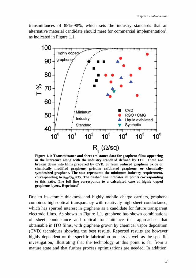
transmittances of 85%-90%, which sets the industry standards that an
alternative material candidate should meet for commercial implementation5,
as indicated in Figure 1.1.
Figure 1.1: Transmittance and sheet resistance data for graphene films appearing
in the literature along with the industry standard defined by ITO. These are
broken down into films prepared by CVD, or from reduced graphene oxide or
chemically modified graphene, pristine exfoliated graphene, or chemically
synthesized graphene. The star represents the minimum industry requirement,
corresponding to DC/Op=35. The dashed line indicates all points corresponding
to this ratio. The full line corresponds to a calculated case of highly doped
graphene layers. Reprinted5
Due to its atomic thickness and highly mobile charge carriers, graphene
combines high optical transparency with relatively high sheet conductance,
which has spurred interest in graphene as a candidate for future transparent
electrode films. As shown in Figure 1.1, graphene has shown combinations
of sheet conductance and optical transmittance that approaches that
obtainable in ITO films, with graphene grown by chemical vapor deposition
(CVD) techniques showing the best results. Reported results are however
highly dependent on the specific fabrication process as well as the specific
investigation, illustrating that the technology at this point is far from a
mature state and that further process optimizations are needed. In addition,
Chapter 1 - Introduction
4
graphene is able to address some of the fundamental drawbacks of ITO films
relating to mechanical fragility and long term degradation. ITO is a very
brittle material and is therefore prone to damage from mechanical straining.
It is therefore not compatible with applications that require mechanical
flexibility, and its electrical properties are shown to degrade in long term
cyclic testing due to formation of micro-cracks already at 2-3% mechanical
strain6. Due to its high mechanical strength and flexibility, graphene may
therefore facilitate development of innovative devices such as flexible solar
panels and flexible displays.
1.2 Graphene applications in high-speed electronics
As formulated and foreseen by Gordon Moore in 1965, the electronics
industry has achieved a mind staggering evolution in the computing power
of integrated circuits over the course of the last 4 decades. He foresaw that
the number of transistors pr. unit area in integrated circuits would double
every 18-24 months (known as Moore's law).
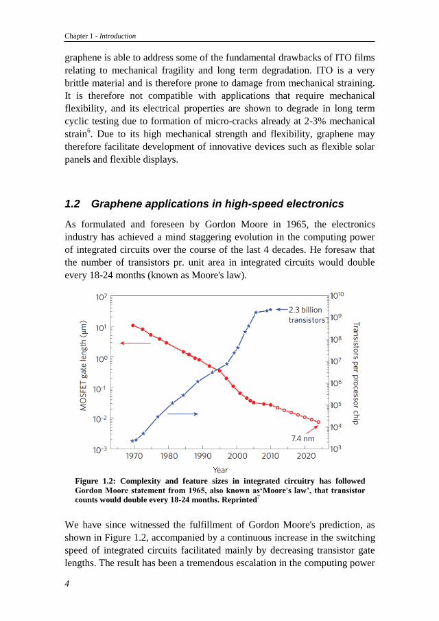
Figure 1.2: Complexity and feature sizes in integrated circuitry has followed
Gordon Moore statement from 1965, also known as‘Moore's law’, that transistor
counts would double every 18-24 months. Reprinted7
We have since witnessed the fulfillment of Gordon Moore's prediction, as
shown in Figure 1.2, accompanied by a continuous increase in the switching
speed of integrated circuits facilitated mainly by decreasing transistor gate
lengths. The result has been a tremendous escalation in the computing power
Chapter 1 - Introduction
5
available from integrated electronics. Moore's law was effectuated by the
impressive advances in silicon processing technology, which have yielded
some of the most complex structures ever created by mankind.
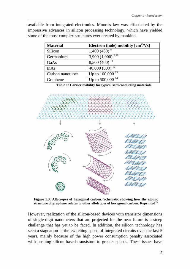
Material Electron (hole) mobility [cm2/Vs]
Silicon 1,400 (450) 8
Germanium 3,900 (1,900) 9,10
GaAs 8,500 (400) 11
InAs 40,000 (500) 12
Carbon nanotubes Up to 100,000 13
Graphene Up to 500,000 14
Table 1: Carrier mobility for typical semiconducting materials.
Figure 1.3: Allotropes of hexagonal carbon. Schematic showing how the atomic
structure of graphene relates to other allotropes of hexagonal carbon. Reprinted15
However, realization of the silicon-based devices with transistor dimensions
of single-digit nanometers that are projected for the near future is a steep
challenge that has yet to be faced. In addition, the silicon technology has
seen a stagnation in the switching speed of integrated circuits over the last 5
years, mainly because of the high power consumption penalty associated
with pushing silicon-based transistors to greater speeds. These issues have
Chapter 1 - Introduction
6
initiated substantial research efforts into alternative materials that can
provide smaller structures or higher switching speeds. Some of the
considered candidates are listed in Table 1.
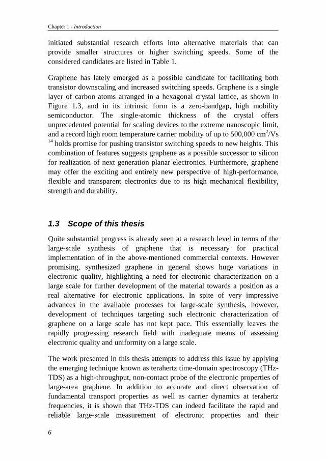
Graphene has lately emerged as a possible candidate for facilitating both
transistor downscaling and increased switching speeds. Graphene is a single
layer of carbon atoms arranged in a hexagonal crystal lattice, as shown in
Figure 1.3, and in its intrinsic form is a zero-bandgap, high mobility
semiconductor. The single-atomic thickness of the crystal offers
unprecedented potential for scaling devices to the extreme nanoscopic limit,
and a record high room temperature carrier mobility of up to 500,000 cm2/Vs
14 holds promise for pushing transistor switching speeds to new heights. This
combination of features suggests graphene as a possible successor to silicon
for realization of next generation planar electronics. Furthermore, graphene
may offer the exciting and entirely new perspective of high-performance,
flexible and transparent electronics due to its high mechanical flexibility,
strength and durability.
1.3 Scope of this thesis
Quite substantial progress is already seen at a research level in terms of the
large-scale synthesis of graphene that is necessary for practical
implementation of in the above-mentioned commercial contexts. However
promising, synthesized graphene in general shows huge variations in
electronic quality, highlighting a need for electronic characterization on a
large scale for further development of the material towards a position as a
real alternative for electronic applications. In spite of very impressive
advances in the available processes for large-scale synthesis, however,
development of techniques targeting such electronic characterization of
graphene on a large scale has not kept pace. This essentially leaves the
rapidly progressing research field with inadequate means of assessing
electronic quality and uniformity on a large scale.
The work presented in this thesis attempts to address this issue by applying
the emerging technique known as terahertz time-domain spectroscopy (THz-
TDS) as a high-throughput, non-contact probe of the electronic properties of
large-area graphene. In addition to accurate and direct observation of
fundamental transport properties as well as carrier dynamics at terahertz
frequencies, it is shown that THz-TDS can indeed facilitate the rapid and
reliable large-scale measurement of electronic properties and their
Chapter 1 - Introduction
7
uniformity in large-scale graphene that might be viewed as a vital
requirement for industrial implementation of the material.
In chapter 2 the electronic properties of graphene are introduced. In
particular, the unusual linear energy dispersion of graphene charge carriers
and its consequences for electronic transport in graphene are described. The
linear dispersion leads to a range of exotic quantum effects including the
half-integer quantum Hall effect (QHE), a non-zero Berry’s phase, as well as
Klein tunneling, leading to de-localization of carriers at low densities.
Perhaps most importantly, the linear dispersion leads to quasi-relativistic
behavior of graphene carriers, which are described analogously to Dirac
Fermions with zero rest mass. It is argued that in the typically observed
diffusive regime dominated by long-range scattering on charged impurities,
the carrier momentum relaxation time scales with the square-root of carrier
density, while the graphene conductance scales linear with carrier density.
On this basis the carrier mobility in graphene is expressed in terms of the
carrier relaxation time, readily evaluated in a Drude framework based on
broadband THz-TDS experiments. The chapter concludes with a description
of the electronic defects specific to large-scale synthesized graphene and
their relation to the concept of preferential carrier back-scattering. This
phenomenon gives rise to distinct features in the THz conductivity, which is
modelled on a phenomenological basis in the Drude-Smith model.
Chapter 3 summarizes the main principles of THz-TDS and provides
descriptions of the experimental methods and setups used for conventional
and ultra-broadband THz-TDS in this thesis.
Chapter 4 presents an experimental study where the THz conductance
response, measured by conventional and ultra-broadband THz-TDS, of
large-area graphene grown by CVD on poly-crystalline and single-
crystalline copper substrates are compared. Carrier momentum relaxation
times are measured directly for both films and used to evaluate the mean free
path and carrier mobility. In addition, qualitatively different transport
characteristics are found for the two films by ultra-broadband THz-TDS,
revealing that preferential carrier back-scattering is significant in the CVD
graphene film grown on poly-crystalline copper. Through comparison with
DC micro four-point probe conductance measurements it is established by a
one-to-one correlation, where 4THz TDS M PP , that the conductance
measured by THz-TDS in the low frequency limit reflects the DC
conductance. Finally, based on this observation, a demonstration of wafer-
Chapter 1 - Introduction
8
scale graphene conductance mapping is presented based on THz time-
domain spectroscopic imaging.
In chapter 5, the characteristics of electrical defects in cm-scale CVD
graphene are investigated by concurrent conductance mapping by THz-TDS
and M4PP. It is shown, on a statistical basis of more than 4000 correlated
conductance measurements, that the nanoscale transport, probed by THz-
TDS, is significantly higher than the micro-scale transport, probed by M4PP.
Based on detailed analysis of the results of the two measurement techniques,
it is concluded that the film is electrically continuous on the nanoscopic
scale, but dominated in its microscopic electronic transport by defects on a
~10 m scale.
Finally, chapter 6 provides an investigation of the electrically gated THz
conductivity in CVD graphene, resulting in a demonstration of large-area
graphene field-effect mobility mapping. To isolate the gate-induced
conductance of the graphene film from that of the underlying gate electrode,
a low-mobility, high carrier density gate material is used. This allows
reliable observation of a THz sheet conductance that varies linearly with gate
voltage and inherent accurate extraction of graphene field effect mobility
and its spatial variation.
Chapter 1 - Introduction
9
Chapter 1 - Introduction
10
11
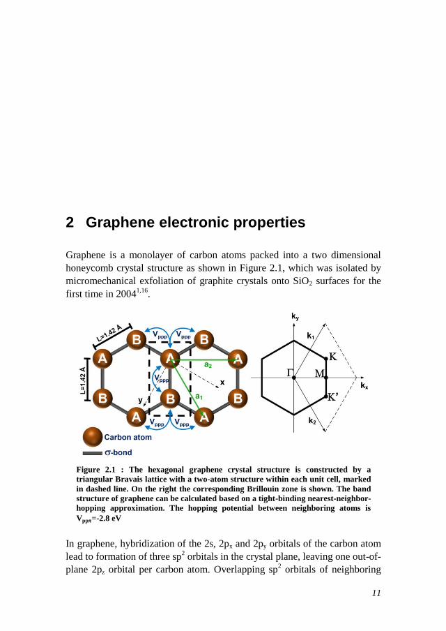
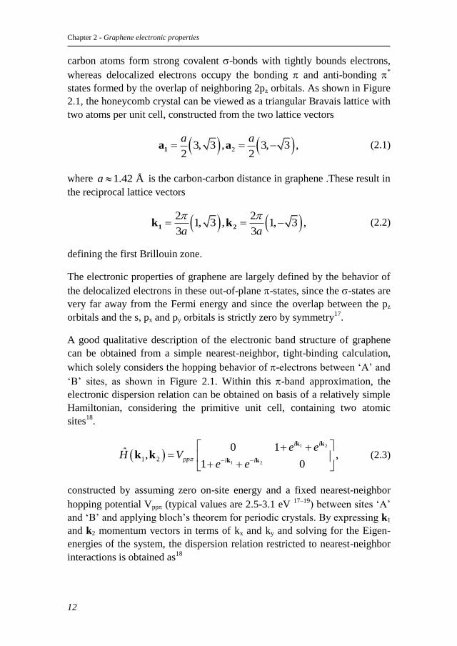
2 Graphene electronic properties
Graphene is a monolayer of carbon atoms packed into a two dimensional
honeycomb crystal structure as shown in Figure 2.1, which was isolated by
micromechanical exfoliation of graphite crystals onto SiO2 surfaces for the
first time in 20041,16
.
Figure 2.1 : The hexagonal graphene crystal structure is constructed by a
triangular Bravais lattice with a two-atom structure within each unit cell, marked
in dashed line. On the right the corresponding Brillouin zone is shown. The band
structure of graphene can be calculated based on a tight-binding nearest-neighbor-
hopping approximation. The hopping potential between neighboring atoms is
Vpp=-2.8 eV
In graphene, hybridization of the 2s, 2px and 2py orbitals of the carbon atom
lead to formation of three sp2 orbitals in the crystal plane, leaving one out-of-
plane 2pz orbital per carbon atom. Overlapping sp2 orbitals of neighboring
Chapter 2 - Graphene electronic properties
12
carbon atoms form strong covalent -bonds with tightly bounds electrons,
whereas delocalized electrons occupy the bonding and anti-bonding *
states formed by the overlap of neighboring 2pz orbitals. As shown in Figure
2.1, the honeycomb crystal can be viewed as a triangular Bravais lattice with
two atoms per unit cell, constructed from the two lattice vectors
23, 3 , 3, 3 ,2 2
a a 1a a (2.1)
where 1.42 Åa is the carbon-carbon distance in graphene .These result in
the reciprocal lattice vectors
2 21, 3 , 1, 3 ,
3 3a a
1 2k k
(2.2)
defining the first Brillouin zone.
The electronic properties of graphene are largely defined by the behavior of
the delocalized electrons in these out-of-plane -states, since the -states are
very far away from the Fermi energy and since the overlap between the pz
orbitals and the s, px and py orbitals is strictly zero by symmetry17
.
A good qualitative description of the electronic band structure of graphene
can be obtained from a simple nearest-neighbor, tight-binding calculation,
which solely considers the hopping behavior of-electrons between ‘A’ and
‘B’ sites, as shown in Figure 2.1. Within this -band approximation, the
electronic dispersion relation can be obtained on basis of a relatively simple
Hamiltonian, considering the primitive unit cell, containing two atomic
sites18
.
1 2
1 21 2
0 1ˆ , ,1 0
i i
pp i i
e eH V
e e
k k
k kk k (2.3)
constructed by assuming zero on-site energy and a fixed nearest-neighbor
hopping potential Vpp (typical values are 2.5-3.1 eV 17–19
) between sites ‘A’
and ‘B’ and applying bloch’s theorem for periodic crystals. By expressing k1
and k2 momentum vectors in terms of kx and ky and solving for the Eigen-
energies of the system, the dispersion relation restricted to nearest-neighbor
interactions is obtained as18
Chapter 2 - Graphene electronic properties
13
3 3, 3 2cos 3 4cos cos ,
2 2x y pp y y x
a aE k k V ak k k
(2.4)
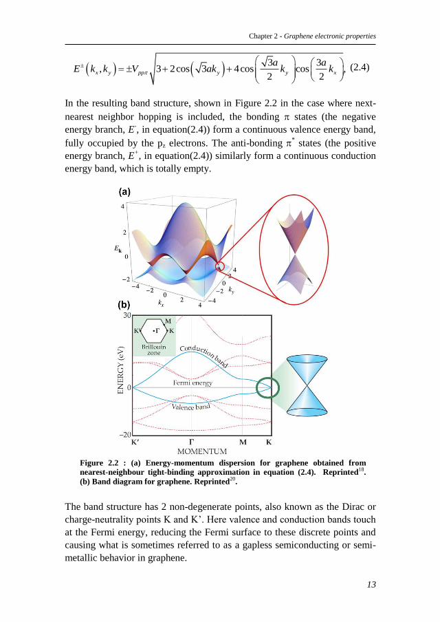
In the resulting band structure, shown in Figure 2.2 in the case where next-
nearest neighbor hopping is included, the bonding states (the negative
energy branch, E-, in equation(2.4)) form a continuous valence energy band,
fully occupied by the pz electrons. The anti-bonding * states (the positive
energy branch, E+, in equation(2.4)) similarly form a continuous conduction
energy band, which is totally empty.
Figure 2.2 : (a) Energy-momentum dispersion for graphene obtained from
nearest-neighbour tight-binding approximation in equation (2.4). Reprinted18.
(b) Band diagram for graphene. Reprinted20.
The band structure has 2 non-degenerate points, also known as the Dirac or
charge-neutrality points K and K’. Here valence and conduction bands touch
at the Fermi energy, reducing the Fermi surface to these discrete points and
causing what is sometimes referred to as a gapless semiconducting or semi-
metallic behavior in graphene.
Chapter 2 - Graphene electronic properties
14
2.1 Linear energy dispersion and massless charge
carriers
One of the most important features of the graphene band structure is the
linear dispersion observed in the distinct cone shape close to the K and K’
points. Through an expansion around the K (or K’) vectors, the low energy
dispersion can be expressed as17,18
2
F( ) v [(q/ K) ],E O q q (2.5)
where x y(k ,k ) q K and q K , and vF is the momentum-
independent electronic group velocity or constant Fermi velocity, given by
6
F
3v 10 m s.
2
ppaV (2.6)
For small q, corresponding to electron energies close to the Fermi energy,
equation (2.5) thus expresses the linear nature of the electronic dispersion.
This feature implies that carrier movement in graphene is analogous to that
of relativistic particles with zero rest mass, described by Dirac's relativistic
equation19
. This stands in grave contrast with conventional solid-state-
systems with parabolic dispersion relations, where carrier transport is
fundamentally described by the Schrödinger equation. The consequence of
this linear electronic spectrum is a condensed matter system in which the
charge carriers move in the crystal with zero effective mass and show many
traits of relativistic quantum electrodynamics even at room temperature2,3
.
Graphene charge carriers thus effectively mimic photon behavior with a rest
mass equal to zero and a group velocity that is roughly 1/300 of the speed of
light, resulting in extraordinarily high mobilities and ballistic transport
across micrometer distances at room temperature2,14,21
.
Amongst the distinctive phenomena arising from the quasi-relativistic nature
of the Dirac fermions in graphene are measured effective carrier masses as
low as 0.007me when approaching the charge-neutrality point3, an anomalous
half-integer quantum hall effect2,3
, observation of a non-zero Berry’s phase3,
as well as Klein tunneling2,18
, where the latter has the effect of inhibiting
carrier localization in the low density limit.
Chapter 2 - Graphene electronic properties
15
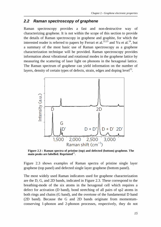
2.2 Raman spectroscopy of graphene
Raman spectroscopy provides a fast and non-destructive way of
characterizing graphene. It is not within the scope of this section to provide
the details of Raman spectroscopy in graphene and graphite, for which the
interested reader is referred to papers by Ferrari et al.22,23
and Yu et al.24
, but
a summary of the most basic use of Raman spectroscopy as a graphene
characterization technique will be provided. Raman spectroscopy provides
information about vibrational and rotational modes in the graphene lattice by
measuring the scattering of laser light on phonons in the hexagonal lattice.
The Raman spectrum of graphene can yield information on the number of
layers, density of certain types of defects, strain, edges and doping level23
.
Figure 2.3 : Raman spectra of pristine (top) and defected (bottom) graphene. The
main peaks are labelled. Reprinted23.
Figure 2.3 shows examples of Raman spectra of pristine single layer
graphene (top panel) and defected single layer graphene (bottom panel).
The most widely used Raman indicators used for graphene characterization
are the D, G, and 2D bands, indicated in Figure 2.3. These correspond to the
breathing-mode of the six atoms in the hexagonal cell which requires a
defect for activation (D band), bond stretching of all pairs of sp2 atoms in
both rings and chains (G band), and the overtone of the fundamental D band
(2D band). Because the G and 2D bands originate from momentum-
conserving 1-phonon and 2-phonon processes, respectively, they do not
Chapter 2 - Graphene electronic properties
16
require a defect for activation and are always present.23
Commonly, the ratio
of D band to G band intensity, D GI I , is used as an indicator of defect
density, as the D band intensity is related lattice defects, edge states and
amorphicity. The intensity of the 2D band shows a significant sensitivity to
the number of graphene layers, for which reason the ratio of 2D to G band
intensity, 2D GI I , is used for identifying the number of layers. Single layer
graphene typically shows ratios of at least 2 1.5D GI I . The width and
shape of the D and 2D peaks, which are well described as single lorentzian
peaks for single layer graphene but splits into a superposition of several
peaks for multiple layers, are used for characterization of the number of
graphene layers in a sample.
The less distinct and seldomly analysed peaks in Figure 2.3 are associated
with an intra-valley double-resonance process (D’ band), a combination of a
D phonon and the D’’ longitudinal acoustic phonon at 1,100 cm-1
(D+D’’
band), a combination of D and D’ phonons, and the overtone of the D’ band. 23
2.3 Electric field effect, minimum conductance and
charge puddles
The possibility of controlling the carrier concentration in semi-metallic few-
layer and monolayer graphene films by utilization of the electric field effect
was first demonstrated by Novoselov et al. in 20041 and by Zhang et al. in
20053, respectively. In the experiments the carrier concentration in the
graphene films was controlled by applying a back-gate voltage in a
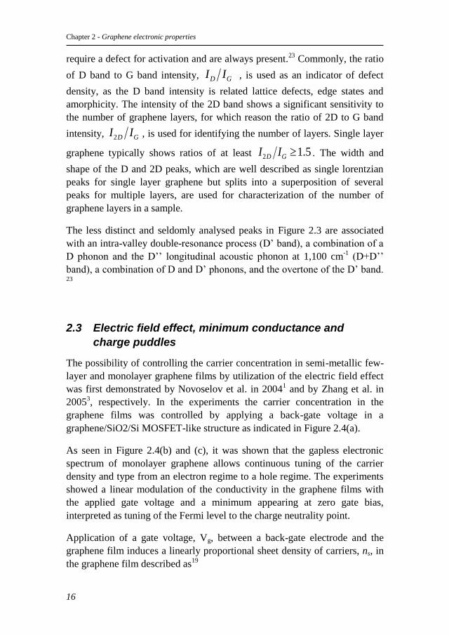
graphene/SiO2/Si MOSFET-like structure as indicated in Figure 2.4(a).
As seen in Figure 2.4(b) and (c), it was shown that the gapless electronic
spectrum of monolayer graphene allows continuous tuning of the carrier
density and type from an electron regime to a hole regime. The experiments
showed a linear modulation of the conductivity in the graphene films with
the applied gate voltage and a minimum appearing at zero gate bias,
interpreted as tuning of the Fermi level to the charge neutrality point.
Application of a gate voltage, Vg, between a back-gate electrode and the
graphene film induces a linearly proportional sheet density of carriers, ns, in
the graphene film described as19
Chapter 2 - Graphene electronic properties
17
1 1 .g g g
s g Q
Q
C C Vn V n
e en
(2.7)
Here Cg is the gate capacitance, e is the electronic charge and
2
22Q g Fn C v e . The second term on the right-hand side of
equation (2.7) is the so-called quantum capacitance. Under typical
experiment conditions with a dielectric constant 4r , and gate dielectric
thickness larger than 50 nm, the quantum capacitance of the system can be
neglected for gate voltages larger than few hundred mV19
.
Figure 2.4 : (a) Schematic of the sample structure used in the initial work on
electric field effect in graphene films. (b) Sheet conductance as a function of back-
gate voltage for a micro-mechanically exfoliated monolayer graphene flake at
T=10K. The slopes reflect a field effect carrier mobility of around 15,000 cm2/Vs.
Reprinted2. (c) Hall measurements of carrier density and Hall mobility as a
function of back-gate voltage at T=1.7K. Reprinted3
Chapter 2 - Graphene electronic properties
18
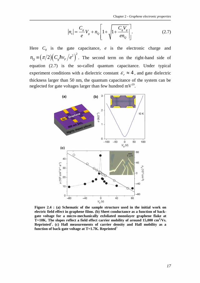
In this case the gate capacitance is given simply as the capacitance of an
ideal plate capacitor with a dielectric medium of dielectric constant r,
0 rCt
, resulting
0 ,rs gn V
t e
(2.8)
where 0 is the vacuum permittivity and t is the thickness of gate dielectric.
Figure 2.5(a) and (b) shows plots of the approximate and full expressions for
the sheet carrier density in electrically gated graphene on 5 Å and 50 nm
SiO2, respectively, illustrating that the quantum capacitance becomes
increasingly important for very thin dielectric layers.
Figure 2.5 : Sheet carrier density calculated from the full expression in equation
(2.7) (red lines) and approximate expression where the quantum capacitance,
expressed in the second term on the right-hand-side is neglected (black lines), for (a)
5 Å SiO2 gate dielectric and (b) 50 nm SiO2 gate dielectric.
For 300 nm SiO2 the proportionality factor 0 r t e is approximately
10 -2 -17.2 10 cm V . The assumption of a voltage-independent capacitance is
valid for highly doped back-gate electrodes where the depletion width is
negligible.
The observed linear dependence of sheet conductance on gate bias was
treated under the framework of a diffusive Drude-type transport regime
where sheet conductance, s, and carrier density, ns, can be related as
0 ,FE rs FE s ge n V
t
(2.9)
and the field effect mobility found as
Chapter 2 - Graphene electronic properties
19
0
.sFE
r g
t
V
(2.10)
It should be noted that this relation only holds true sufficiently far away from
the charge-neutrality point where a majority carrier density is well-defined19
.
This treatment led to extraction of carrier mobilities on the order of 10.000-
15.000 cm2/Vs
1–3, which agrees with Hall mobility measurements, as shown
in Figure 2.4(c).
Figure 2.6 : (a) The minimum conductivity and metallic-regime-mobility (mL) for
19 different graphene devices measured at 1.6 K. Filled symbols indicate two
devices made from the same graphene flake, as shown in the inset. Reprinted32 (b)
Colour map of the spatial carrier density variations in a graphene flake, extracted
from surface potential measurements. The blue regions correspond to holes and
the red regions to electrons. Reprinted33. (c) Histogram of the density fluctuations
in (b). Reprinted33
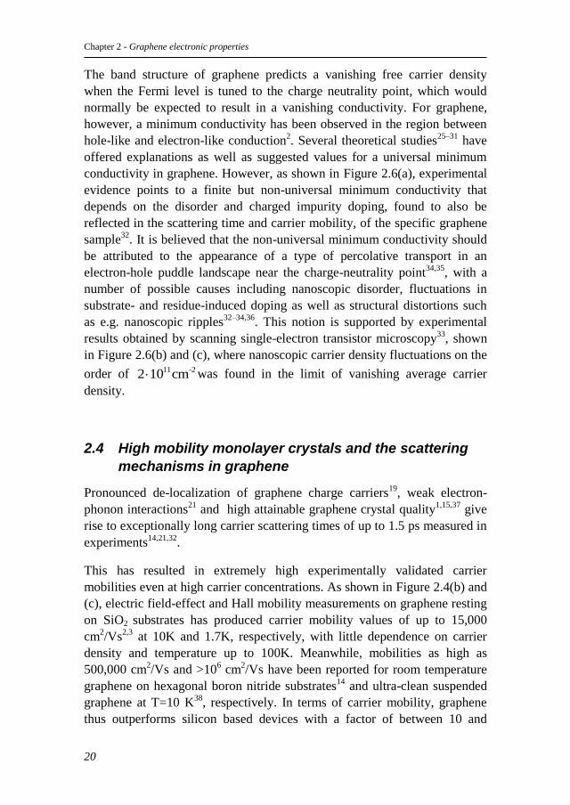
Chapter 2 - Graphene electronic properties
20
The band structure of graphene predicts a vanishing free carrier density
when the Fermi level is tuned to the charge neutrality point, which would
normally be expected to result in a vanishing conductivity. For graphene,
however, a minimum conductivity has been observed in the region between
hole-like and electron-like conduction2. Several theoretical studies
25–31 have
offered explanations as well as suggested values for a universal minimum
conductivity in graphene. However, as shown in Figure 2.6(a), experimental
evidence points to a finite but non-universal minimum conductivity that
depends on the disorder and charged impurity doping, found to also be
reflected in the scattering time and carrier mobility, of the specific graphene
sample32
. It is believed that the non-universal minimum conductivity should
be attributed to the appearance of a type of percolative transport in an
electron-hole puddle landscape near the charge-neutrality point34,35
, with a
number of possible causes including nanoscopic disorder, fluctuations in
substrate- and residue-induced doping as well as structural distortions such
as e.g. nanoscopic ripples32–34,36
. This notion is supported by experimental
results obtained by scanning single-electron transistor microscopy33
, shown
in Figure 2.6(b) and (c), where nanoscopic carrier density fluctuations on the
order of 11 -22 10 cm was found in the limit of vanishing average carrier
density.
2.4 High mobility monolayer crystals and the scattering
mechanisms in graphene
Pronounced de-localization of graphene charge carriers19
, weak electron-
phonon interactions21
and high attainable graphene crystal quality1,15,37
give
rise to exceptionally long carrier scattering times of up to 1.5 ps measured in
experiments14,21,32
.
This has resulted in extremely high experimentally validated carrier
mobilities even at high carrier concentrations. As shown in Figure 2.4(b) and
(c), electric field-effect and Hall mobility measurements on graphene resting
on SiO2 substrates has produced carrier mobility values of up to 15,000
cm2/Vs
2,3 at 10K and 1.7K, respectively, with little dependence on carrier
density and temperature up to 100K. Meanwhile, mobilities as high as
500,000 cm2/Vs and >10
6 cm
2/Vs have been reported for room temperature
graphene on hexagonal boron nitride substrates14
and ultra-clean suspended
graphene at T=10 K38
, respectively. In terms of carrier mobility, graphene
thus outperforms silicon based devices with a factor of between 10 and
Chapter 2 - Graphene electronic properties
21
~600. Significantly higher carrier mobilities have been observed in GaAs 2D
electron gases (2DEG) at cryogenic temperatures, however, as shown in
Figure 2.7 these structures show much lower mobilities at room
temperature39
, due to carrier dynamics mainly limited by phonon-
interactions.
Figure 2.7 : The mobility progress achieved at Bell Labs for GaAs 2DEGs over the
last three decades, leading up to the present mobility record of 36.000.000 cm2/Vs.
The curve labelled ‘bulk’ is for GaAs single crystal doped with the same
concentration of electrons as the 2DEGs. MBE: molecular-beam epitaxy; LN2:
liquid nitrogen; ‘undoped setback’: and undoped layer prior to the modulation
doping to further separate the ionized impurities from the 2DEG. Reprinted39.
The high mobilities and long carrier scattering times observed in graphene
experiments are quite remarkable testaments to the de-localization and weak
interaction of Dirac Fermions as well as to a high graphene crystal quality1–
3,16,37,40. This is perhaps best appreciated by considering that in a material
with a Fermi velocity as high as 6
Fv 10 m s , the observed scattering
times correspond to ballistic transport across mean free paths, vFl ,
Chapter 2 - Graphene electronic properties
22
upwards of 1.5 m at room temperature in a 2D electron gas which is at
most separated from material interfaces by a few Å1,14
.
Although the carrier scattering mechanisms in graphene include carrier-
carrier and carrier-phonon collisions, recent theoretical18,19,34,35,41
and
experimental work32,36
indicates that diffusive carrier transport is limited by
short-ranged scattering on neutral crystal defects and long-range scattering
on extrinsic charged impurities, giving rise to two qualitative different
behaviors in transport experiments.
Charge transport dominated by short-ranged scattering, with a 1 n
dependence of the momentum-averaged carrier scattering time, , predicted
from Boltzmann transport theory19,34,35
, is expected to result in a density-
independent conductivity18,19,21,34,35,42
since
2
,Fe vn
(2.11)
which is also obtained for graphene in the framework of Boltzmann transport
theory19,34,35,42
. In contrast, graphene carrier transport dominated by long-
range scattering on charged impurities yields a n dependence18,19,34,35
,
resulting in conductance that depends linearly on carrier density as expressed
by equation (2.11)18,19,34,35
, in agreement with experimental results. This also
provides a relation between carrier mobility and carrier scattering time
within the regime of long-range impurity scattering. Since en we have
.Fev
n
(2.12)
Short-range scattering is expected to have significance only when charged
impurities, with density ni, are effectively screened in the high-density-limit
when in n 19,34,35. The influence of short-range scattering is thus expected
to be observable primarily in ultra-clean samples where ni is small.
As shown in Figure 2.8(a), (b) and (c), recent transport experiments on very
clean graphene samples have shown sub-linear (Vg) consistent with
transport where both short-range and long-range scattering have significant
contributions21,32,36
. In experiments where potassium ions, acting as charged
impurities, were deposited in-situ on a graphene flake in ultra-high vacuum
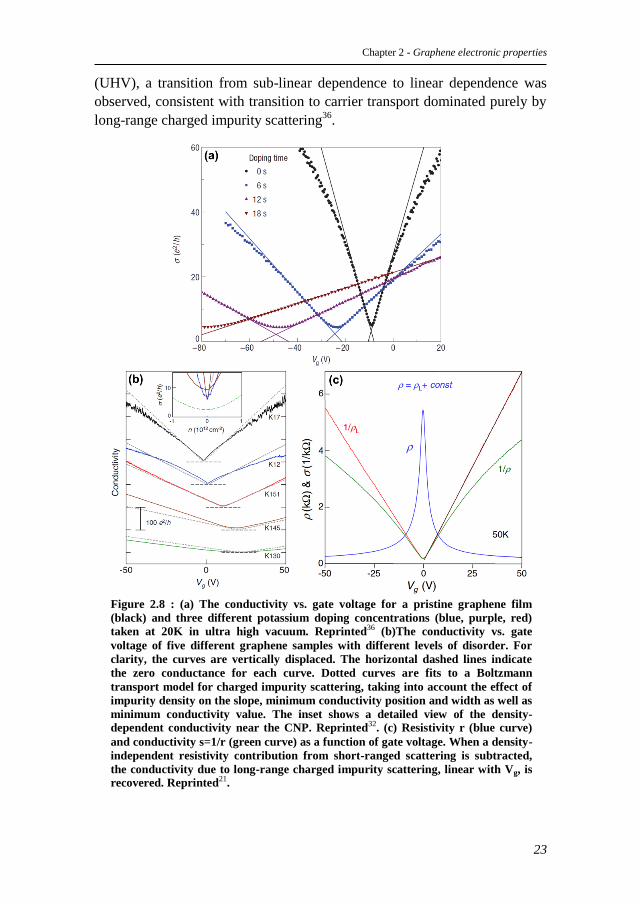
Chapter 2 - Graphene electronic properties
23
(UHV), a transition from sub-linear dependence to linear dependence was
observed, consistent with transition to carrier transport dominated purely by
long-range charged impurity scattering36
.
Figure 2.8 : (a) The conductivity vs. gate voltage for a pristine graphene film
(black) and three different potassium doping concentrations (blue, purple, red)
taken at 20K in ultra high vacuum. Reprinted36 (b)The conductivity vs. gate
voltage of five different graphene samples with different levels of disorder. For
clarity, the curves are vertically displaced. The horizontal dashed lines indicate
the zero conductance for each curve. Dotted curves are fits to a Boltzmann
transport model for charged impurity scattering, taking into account the effect of
impurity density on the slope, minimum conductivity position and width as well as
minimum conductivity value. The inset shows a detailed view of the density-
dependent conductivity near the CNP. Reprinted32. (c) Resistivity r (blue curve)
and conductivity s=1/r (green curve) as a function of gate voltage. When a density-
independent resistivity contribution from short-ranged scattering is subtracted,
the conductivity due to long-range charged impurity scattering, linear with Vg, is
recovered. Reprinted21.
Chapter 2 - Graphene electronic properties
24
Based on Boltzmann theory for graphene transport dominated by long-range
charged impurity scattering a semi-classical, Drude-type expression for the
frequency-dependent conductivity can thus be constructed18,34,41–44
:
,1
DC
i
(2.13)
where
2
.FDC
e vn
It should be noted that in this expression is the
carrier density-dependent scattering time, expected to scale with n . The
basics of the classical Drude model are explained in the following section.
2.5 The Drude model
The Drude model is a classical model for the transport dynamics of free
massive charge carriers under influence of an electric field, E, in solid state
systems in the diffusive regime. In its classical formulation presented here,
some aspects of the model, such as e.g. the notion of a finite carrier mass,
does not apply directly for description of the massless Dirac fermions in
graphene. However, graphene charge carrier dynamics have been shown to
be phenomenologically well described by the Drude form, and it may serve
as a good basis for understanding the concepts of diffusive carrier transport
in graphene, limited by random scattering events.
The Drude model considers the kinetics of the free charge carriers as
analogous to that of molecules in a gas, by describing the system as
comprised of completely free and independent carriers moving ballistically
between randomly occurring elastic scattering events. A basic assumption of
the model is that a collision results in complete randomization of the carrier
momentum and thermalization with the surroundings, and that the
occurrence of collisions is described by an average, characteristic rate,
, where is the average time between collisions. The average
equation of motion of charge carriers can be deduced by considering the first
time-derivative of carrier momentum, t dt t
t dt
p pp. According to
the model assumptions there is a CP dt chance of collision, resulting in
an average momentum 0C t dt p , while there is a 1NCP dt
Chapter 2 - Graphene electronic properties
25
chance that no collision will occur, resulting in the momentum evolving
unhindered as NC t dt t t dt p p F . The new average momentum is
thus
1 ,
C C NC NCt dt P t dt P t dt
dtt t dt
p p p
p F (2.14)
which enables evaluation of the first time-derivative of momentum,
expressing the equation of motion averaged over charge carriers
0
lim .dt
t dt t tdt
dt dt
p p ppF (2.15)
This may analogously be written as
*
* mm t e t
dt
vv E (2.16)
where m* is the effective mass of charge carriers, when moving between
collisions, e is the electronic charge, and v is the velocity of charge carriers.
The desired solution for a response to an applied electric field with
frequency , ( ) i tRe t Re e E E , is of the form
( ) i tRe t Re e v v . Inserting E(t) and v(t) in equation (2.16)
yields
*
,m
i e
v v E (2.17)
which can be rewritten as
*
,1
e m
i
v
E (2.18)
By using the definition
en
J v
E E
, we arrive at the complex,
frequency-dependent conductivity
Chapter 2 - Graphene electronic properties
26
2 *
,1 1
DCne m
i i
(2.19)
where 2 *
DC ne m is the conductivity at 0 . Explicitly separated in
real and imaginary parts, it becomes
2
1
1real DC
(2.20)
21
imag DC
(2.21)
In a steady-state situation, where 0dv dt , equation (2.16) reduces to
*
,e
m
v
E (2.22)
defining the carrier mobility, , which is the ratio of the average drift
velocity of the carrier distribution to the electric field. Combined with the
expression for DC, the well-known relation DC en is obtained.
2.6 Defects in large-scale graphene
Though initially fabricated by micro-mechanical exfoliation of graphite,
which is a labour-intensive process yielding small quantities of graphene
flakes of typically 10-100 m lateral dimensions1, a multitude of techniques
for production of graphene on a large scale are now available. Although the
performance gap is rapidly shrinking45,46
, graphene produced in large scale
methods so far provides electronic properties that are highly varying and in
most cases inferior to that of mechanically exfoliated graphene. In the
following, short descriptions are given of the most widely applied methods
for large-scale graphene production, to provide a qualitative understanding
of the type of defects expected to degrade the electronic properties of large-
area graphene compared to its mechanically exfoliated counterpart as well as
a qualitative understanding of their impact on electronic properties.
Chapter 2 - Graphene electronic properties
27
The most common large-scale fabrication techniques include bulk
production using liquid-phase exfoliation of graphite or graphite oxide47–50
and large-area synthesis by epitaxial growth from high temperature
sublimation of silicon from silicon-carbide (SiC) surfaces51–53
as well as
chemical growth by catalyzed chemical vapor deposition54,55
. In principle
there are no fundamental limitations on the size of graphene films that can be
obtained from these methods, and films with dimensions of several to tens of
inches have already been demonstrated by liquid-phase exfoliaton56
and
CVD processing57
, respectively. However, the currently available size of SiC
substrates means that the epitaxial growth method is in practice limited to 4
inch wafer sizes.
2.6.1 Liquid-phase exfoliation
In liquid-phase exfoliation, large-area films are obtained from graphene47,50
or reduced graphene oxide48
(r-GO) flakes dispersed in a liquid solution, by
e.g. spin-coating, spray-coating or Langmuir-blodgett methods. A slurry of
few-layer flakes is typically obtained by sonication of graphite or graphite
oxide in a solvent or surfactant with suitable surface energy. By subsequent
centrifugation47
, and an added chemical reduction step in the case of graphite
oxide48
, a dispersion of primarily few-layer graphene or r-GO flakes can be
obtained. The average lateral flake dimensions obtained in films prepared
from this technique is typically on the order of few m, as graphite or
graphite oxide crystallites are known to be torn during the sonication
procedure.
2.6.2 Epitaxial growth on SiC
Epitaxial growth of graphene from SiC substrates51–53
is based on the
formation of the graphene crystal structure on the surface of a SiC substrate
by thermal sublimation of silicon and decomposition of the surface at
temperatures typically in the range 1200-1800o C. Epitaxial graphene growth
in inert Argon atmosphere has been shown to allow higher growth
temperatures, resulting in larger homogeneous graphene flakes of up to few
micrometer in width and hundreds of micrometer in length, primarily limited
by terrace steps in the surface morphology of the starting SiC substrate52
.
Growth of multilayer graphene films on the SiC(0001) C-face does however
produce much larger continuous and uniform regions51,58
. Graphene layers
grown by thermal decomposition of SiC surfaces show some chemical
interaction with the underlying substrate, however, quasi-isolated graphene
layers with electronic properties similar to that of isolated graphene
Chapter 2 - Graphene electronic properties
28
monolayers are observed in parts of multi-layer structures separated from the
substrate by a few graphite inter-layer distances51
.
2.6.3 Chemical vapor deposition on metal catalysts
The chemical vapor deposition (CVD) of graphene films onto metal
substrates54,59
rely on the catalyzed decomposition of carbon pre-cursors in a
gaseous phase, often in the form of CH4 or C2H4, and their structuring into
the graphene honeycomb crystal structure. In particular, Ni59
and Cu54
have
been demonstrated as suitable catalytic growth substrates, yielding both
monolayer and few-layer large-area graphene films. The catalytic growth is
typically carried out at low pressures and temperatures close to 1000o C
54,59,
yielding poly-crystalline monolayer or multi-layer graphene films with grain
sizes on the order of 10 m across60
. The poly crystallinity of deposited
films is usually attributed to growth proceeding from a high density of
nucleation sites or discontinuous growth across metal substrate grain
boundaries60–63
. The deposited graphene films can be transferred to
insulating substrates, appropriate for electronic utilization, by a number of
techniques typically involving sacrificial etching of the metal catalyst
substrate55
. Growth and transfer of 30-inch CVD graphene films have been
demonstrated, as well as their subsequent use as transparent electrode for
touch-screens57
.
2.6.4 Extended defects in large-area graphene
Common for the above-mentioned large-scale production techniques is that
they all produce graphene with more defects than micro-mechanically
exfoliated graphene, resulting in a generally lower and highly varying
electronic quality. Imperfect growth in epitaxially grown and chemical
vapour deposited graphene as well as incomplete reduction47,50
subsequent to
graphite oxidation in liquid-phase exfoliated graphene is likely to lead to an
increased density of crystal defects.
In additions to this, it is expected that flake and grain boundaries in the poly-
crystalline graphene films can form significant extended electronic
barriers64
, which in particular are expected to degrade long-range transport62
.
In addition to degrading the DC conductivity of the graphene films, the
existence of such extended defects can lead to perturbation of the
characteristic form of the frequency-dependent conductivity, by causing
preferential back-scattering of charge carriers. In AC transport measurement,
such as a THz-TDS investigation, the probing length scale in a diffusive
Chapter 2 - Graphene electronic properties
29
regime is defined by the frequency as 2L D f , where D is the
diffusion constant and f is the frequency. This can be thought of as the
distance that a charge carrier moves within one half period of an oscillating
electric field. Back-scattering by defects on a characteristic length scale will
therefore primarily affect the conductivity response at lower frequencies
corresponding to a probing length that is larger than the characteristic defect
length scale. Put differently, a charge carrier cannot respond as effectively to
the applied field if it is confined within the probing length scale. Despite
predictions of de-localization and suppressed back-scattering at electronic
barriers, due to Klein tunneling of chiral, quasi-relativistic graphene charge
carriers18
, we present observations of pronounced signatures of preferential
back-scattering in CVD graphene in our experimental studies in chapter 4.
In the following section, the consequences for the frequency dependent
conductivity in the THz range of such extended defects and their preferential
back-scattering of charge carriers are considered in the framework of the
Drude-Smith model.
2.7 The Drude-Smith Model
The Drude-smith model is a classical model, developed by N.V. Smith, that
aims to incorporate the phenomenon of preferential carrier back-scattering,
or persistence of carrier velocity in scattering events, within a diffusive
transport picture similar to the Drude framework65
. It was developed with the
goal of reproducing the conductivity features of a range of disordered
conductive materials that could not be accurately described by the Drude
model, such as quasi-crystals65,66
, percolative systems67
, and nanocrystalline
systems68–71
. Such materials show a suppression in the low frequency
real(), rising to a peak at non-zero frequency, accompanied by a imag()
that can go negative in the low frequency range.
To account for back-scattering the Drude-Smith model parts with one of the
fundamental assumptions of the Drude model, stating that a carrier scattering
event results in complete momentum randomization. This is necessary, as
back-scattering specifically implies that the carrier momentum, k is reversed
to –k. Put differently, a key concept in the Drude-Smith model is the
introduction of a memory effect that allows the momentum of carriers prior
to a scattering event to influence the momentum subsequent to a scattering
event.
Chapter 2 - Graphene electronic properties
30
N.V. Smith introduced this memory effect on basis of the impulse response
formalism, where the frequency dependent conductivity is found as the
Fourier transform of the impulse current response function. He expressed the
current response function using Poisson statistics as
/
1
( ) / (0) e 1 ,!
n
t
n
n
tj t j c
n
(2.23)
where cn is the fraction of the carrier momentum retained after the nth
scattering event. This should be viewed in contrast to the corresponding
current impulse response function for the Drude model, which is a single
exponential decay. The Fourier transform of equation (2.23) leads to the
Drude-Smith model for frequency dependent conductivity:
1
1 ,1 1
nD
nn
cW
i i
(2.24)
where 2 *
DW ne m is the Drude-weight. Normally, persistence of
velocity is only considered for the first collision subsequent to carrier
excitation, corresponding to inclusion of only the first term in the sum in
equations (2.23) and(2.24). This has the meaning that only the first scattering
event deviates from the regular isotropic Drude scattering mechanism, and
momentum memory thus goes only as far back as prior to the last collision
experienced by the charge carrier. By inclusion of only the first term in the
sum, equation (2.24) can be written explicitly in real and imaginary parts as
2 2 2
22 2
1 ( ) 11
Dreal
Wc
(2.25)
2
22 2
1 ( ) 21
Dimag
Wc
(2.26)
where c1 is now denoted c. Here, only values of c ranging from 0 to -1 are
considered, as these correspond to the situation where velocity is
predominantly or fully negated in scattering events, therefore reflecting
back-scattering of carriers.Figure 2.9 shows the real and imaginary parts of
the Drude-Smith conductivity given in equations (2.25) and (2.26)
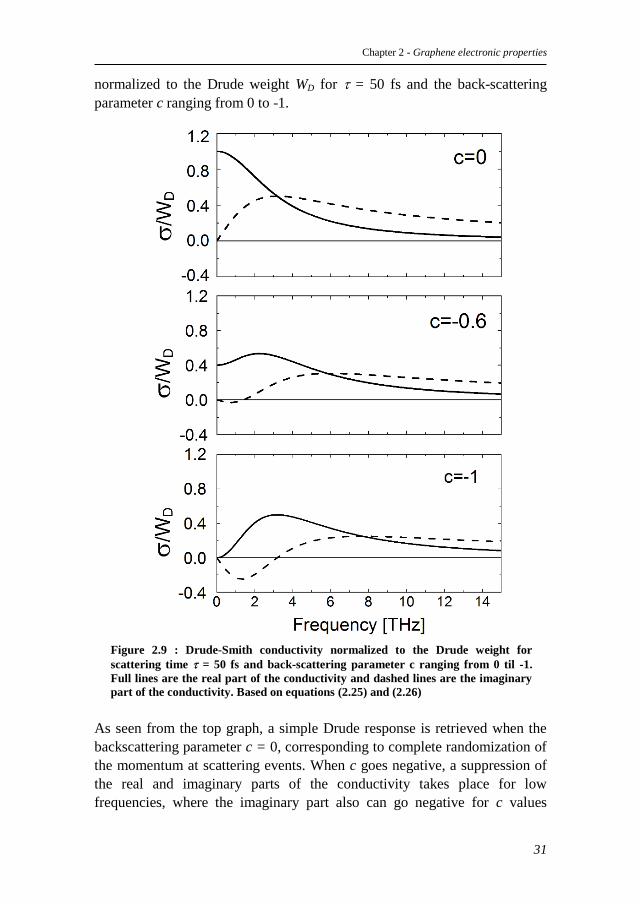
Chapter 2 - Graphene electronic properties
31
normalized to the Drude weight WD for = 50 fs and the back-scattering
parameter c ranging from 0 to -1.
Figure 2.9 : Drude-Smith conductivity normalized to the Drude weight for
scattering time = 50 fs and back-scattering parameter c ranging from 0 til -1.
Full lines are the real part of the conductivity and dashed lines are the imaginary
part of the conductivity. Based on equations (2.25) and (2.26)
As seen from the top graph, a simple Drude response is retrieved when the
backscattering parameter c = 0, corresponding to complete randomization of
the momentum at scattering events. When c goes negative, a suppression of
the real and imaginary parts of the conductivity takes place for low
frequencies, where the imaginary part also can go negative for c values
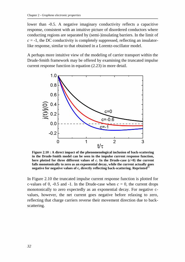
Chapter 2 - Graphene electronic properties
32
lower than -0.5. A negative imaginary conductivity reflects a capacitive
response, consistent with an intuitive picture of disordered conductors where
conducting regions are separated by (semi-)insulating barriers. In the limit of
c = -1, the DC conductivity is completely suppressed, reflecting an insulator-
like response, similar to that obtained in a Lorentz-oscillator model.
A perhaps more intuitive view of the modeling of carrier transport within the
Drude-Smith framework may be offered by examining the truncated impulse
current response function in equation (2.23) in more detail.
Figure 2.10 : A direct impact of the phenomenological inclusion of back-scattering
in the Drude-Smith model can be seen in the impulse current response function,
here plotted for three different values of c. In the Drude-case (c=0) the current
falls monotonically to zero as an exponential decay, while the current actually goes
negative for negative values of c, directly reflecting back-scattering. Reprinted65
In Figure 2.10 the truncated impulse current response function is plotted for
c-values of 0, -0.5 and -1. In the Drude-case when c = 0, the current drops
monotonically to zero expectedly as an exponential decay. For negative c-
values, however, the net current goes negative before relaxing to zero,
reflecting that charge carriers reverse their movement direction due to back-
scattering.
Chapter 2 - Graphene electronic properties
33
Chapter 2 - Graphene electronic properties
34
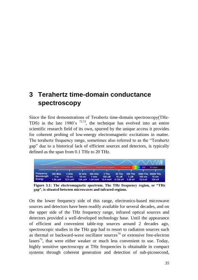
35
3 Terahertz time-domain conductance
spectroscopy
Since the first demonstrations of Terahertz time-domain spectroscopy(THz-
TDS) in the late 1980’s 72,73
, the technique has evolved into an entire
scientific research field of its own, spurred by the unique access it provides
for coherent probing of low-energy electromagnetic excitations in matter.
The terahertz frequency range, sometimes also referred to as the “Terahertz
gap” due to a historical lack of efficient sources and detectors, is typically
defined as the span from 0.1 THz to 20 THz.
Figure 3.1: The electromagnetic spectrum. The THz frequency region, or “THz
gap”, is situated between microwaves and infrared regions.
On the lower frequency side of this range, electronics-based microwave
sources and detectors have been readily available for several decades, and on
the upper side of the THz frequency range, infrared optical sources and
detectors provided a well-developed technology base. Until the appearance
of efficient and convenient table-top sources around 2 decades ago,
spectroscopic studies in the THz gap had to resort to radiation sources such
as thermal or backward-wave oscillator sources74
or extensive free-electron
lasers75
, that were either weaker or much less convenient to use. Today,
highly sensitive spectroscopy at THz frequencies is obtainable in compact
systems through coherent generation and detection of sub-picosecond,
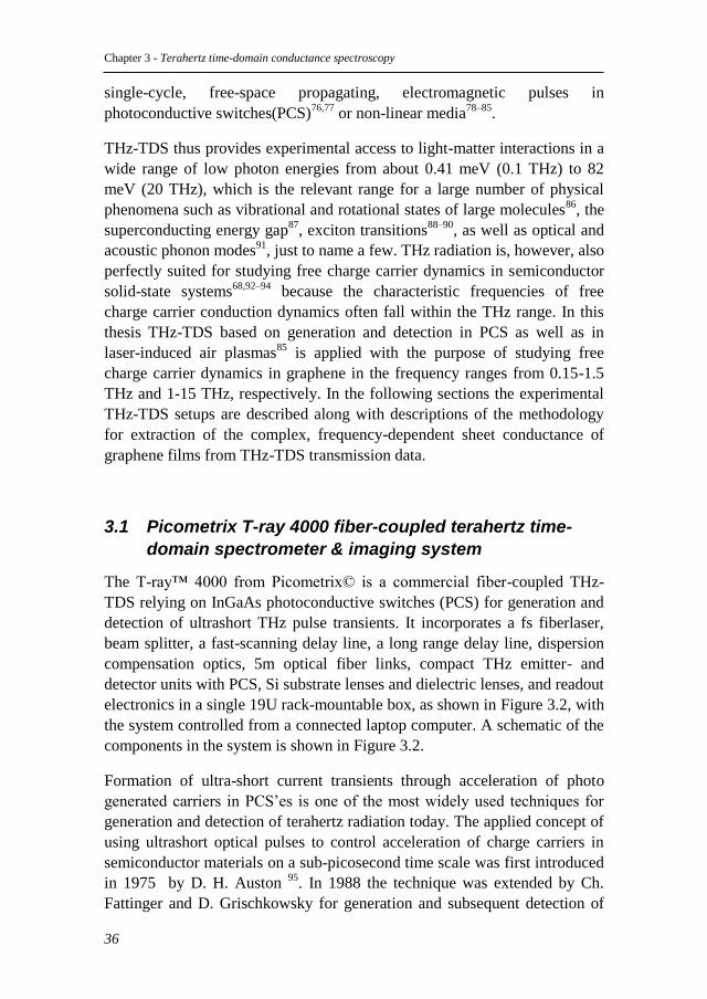
Chapter 3 - Terahertz time-domain conductance spectroscopy
36
single-cycle, free-space propagating, electromagnetic pulses in
photoconductive switches(PCS)76,77
or non-linear media78–85
.
THz-TDS thus provides experimental access to light-matter interactions in a
wide range of low photon energies from about 0.41 meV (0.1 THz) to 82
meV (20 THz), which is the relevant range for a large number of physical
phenomena such as vibrational and rotational states of large molecules86
, the
superconducting energy gap87
, exciton transitions88–90
, as well as optical and
acoustic phonon modes91
, just to name a few. THz radiation is, however, also
perfectly suited for studying free charge carrier dynamics in semiconductor
solid-state systems68,92–94
because the characteristic frequencies of free
charge carrier conduction dynamics often fall within the THz range. In this
thesis THz-TDS based on generation and detection in PCS as well as in
laser-induced air plasmas85
is applied with the purpose of studying free
charge carrier dynamics in graphene in the frequency ranges from 0.15-1.5
THz and 1-15 THz, respectively. In the following sections the experimental
THz-TDS setups are described along with descriptions of the methodology
for extraction of the complex, frequency-dependent sheet conductance of
graphene films from THz-TDS transmission data.
3.1 Picometrix T-ray 4000 fiber-coupled terahertz time-
domain spectrometer & imaging system
The T-ray™ 4000 from Picometrix© is a commercial fiber-coupled THz-
TDS relying on InGaAs photoconductive switches (PCS) for generation and
detection of ultrashort THz pulse transients. It incorporates a fs fiberlaser,
beam splitter, a fast-scanning delay line, a long range delay line, dispersion
compensation optics, 5m optical fiber links, compact THz emitter- and
detector units with PCS, Si substrate lenses and dielectric lenses, and readout
electronics in a single 19U rack-mountable box, as shown in Figure 3.2, with
the system controlled from a connected laptop computer. A schematic of the
components in the system is shown in Figure 3.2.
Formation of ultra-short current transients through acceleration of photo
generated carriers in PCS’es is one of the most widely used techniques for
generation and detection of terahertz radiation today. The applied concept of
using ultrashort optical pulses to control acceleration of charge carriers in
semiconductor materials on a sub-picosecond time scale was first introduced
in 1975 by D. H. Auston 95
. In 1988 the technique was extended by Ch.
Fattinger and D. Grischkowsky for generation and subsequent detection of
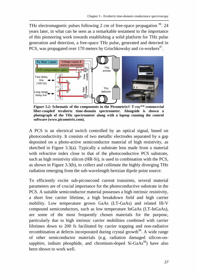
Chapter 3 - Terahertz time-domain conductance spectroscopy
37
THz electromagnetic pulses following 2 cm of free-space propagation 96
. 24
years later, in what can be seen as a remarkable testament to the importance
of this pioneering work towards establishing a solid platform for THz pulse
generation and detection, a free-space THz pulse, generated and detected in
PCS, was propagated over 170 meters by Grischkowsky and co-workers97
.
Figure 3.2: Schematic of the components in the Picometrix© T-ray™ commercial
fiber-coupled terahertz time-domain spectrometer. Alongside is shown a
photograph of the THz spectrometer along with a laptop running the control
software (www.picometrix.com).
A PCS is an electrical switch controlled by an optical signal, based on
photoconductivity. It consists of two metallic electrodes separated by a gap
deposited on a photo-active semiconductor material of high resistivity, as
sketched in Figure 3.3(a). Typically a substrate lens made from a material
with refractive index close to that of the photoconductive PCS substrate,
such as high resistivity silicon (HR-Si), is used in combination with the PCS,
as shown in Figure 3.3(b), to collect and collimate the highly diverging THz
radiation emerging from the sub-wavelength hertzian dipole point source.
To efficiently excite sub-picosecond current transients, several material
parameters are of crucial importance for the photoconductive substrate in the
PCS. A suitable semiconductor material possesses a high intrinsic resistivity,
a short free carrier lifetime, a high breakdown field and high carrier
mobility. Low temperature grown GaAs (LT-GaAs) and related III-V
compound semiconductors, such as low temperature InGaAs (LT-InGaAs),
are some of the most frequently chosen materials for the purpose,
particularly due to high intrinsic carrier mobilities combined with carrier
lifetimes down to 200 fs facilitated by carrier trapping and non-radiative
recombination at defects incorporated during crystal growth98
. A wide range
of other semiconductor materials (e.g. radiation damaged silicon-on-
sapphire, indium phosphide, and chromium-doped Si-GaAs98
) have also
been shown to work well.
Chapter 3 - Terahertz time-domain conductance spectroscopy
38
Figure 3.3: Schematic layout of traditional photoconductive switches. (a) Front
view of a PCS showing the metallic electrode and photoconductive gap forming the
Hertzian dipole antenna responsible for THz emission. (b) Side view showing the
HR-Si substrate lens used to collect and collimate the highly diverging THz
radiation emerging from the Hertzian dipole point-source. (c) Top view showing
the configurational scheme for THz generation in a PCS. (d) Top view showing the
conigurational scheme for THz detection in a PCS.
When a PCS is utilized for generation of THz pulses a bias voltage, Vbias, is
applied across the dipole gap as indicated in Figure 3.3(a). The dipole gap is
then short-circuited on an ultra-short timescale by illuminating the gap with
a fs optical laser pulse, as indicated in Figure 3.3(c). This creates a dense,
electrically conducting electron-hole gas in the gap region with a lifetime
determined by the carrier trapping time, t, of the semiconductor material.
The photo excited free electrons and holes are accelerated by the electric
field in the gap, Egap(t), which is a superposition of the applied bias field and
a time-dependent opposing field created by the separation of positive (photo-
generated holes) and negative (photo-generated electrons) charges. This
results in a current transient described by the relations
( )t en t J v (3.1)
( )t
dn nG t
dt (3.2)
*
( )gap
s
d (t) et
dt m
v vE (3.3)
( )
( ) scgap bias
tt
PE E (3.4)
Chapter 3 - Terahertz time-domain conductance spectroscopy
39
( )sc sc
r
dt
dt
P PJ (3.5)
where e is the electronic charge, v(t) is the carrier velocity, n is the density of
free carriers, G(t) describes the photo-generation of free carriers, s is the
momentum relaxation scattering time, m* is the effective carrier mass, Ebias is
the electric field due to an applied bias voltage, Psc(t) is the time-dependent
polarization due to space-charge region created by the separation of positive
(photo-generated holes) and negative (photo-generated electrons) charges,
is the permittivity of the substrate, is a geometrical factor, and r is the
carrier recombination time. The electromagnetic radiation emitted due to the
resulting current transient can be described self-consistently on basis of
Maxwell’s equations99
THz
THz
tt
t
HE (3.6)
THz
THz
t tt t
t
EH J (3.7)
where ETHz(t) is the radiated electrical field, HTHz(t) is the radiated magnetic
field and is the permeability of the substrate.
When a PCS is used for detection of THz pulses, the bias voltage source
shown in Figure 3.3(a) is replaced by a current detection across the gap. In
the PCS detection scheme the electric field of the THz pulse acts as a
transient bias on any free carriers, inducing a current transient proportional
to the THz electric field, of which the time-integrated value can be measured
as a quasi-DC signal by means of electronic readout. Relying on the short
free carrier lifetime of a PCS substrate which is much shorter than the THz
pulse, time-gating the presence of free carriers in the PCS gap on an ultra-
short timescale by photo-excitation with fs laser pulses, as indicated in
Figure 3.3(d), facilitates time-resolved measurement of the THz electric
field. The photocurrent, Jmeasured, across the PCS gap is given by the
convolution of the transient surface photoconductivity, s,photo(t), and the
THz electric field profile98
, ' ( ') '
t
measured s photo THzJ t t E t dt
(3.8)
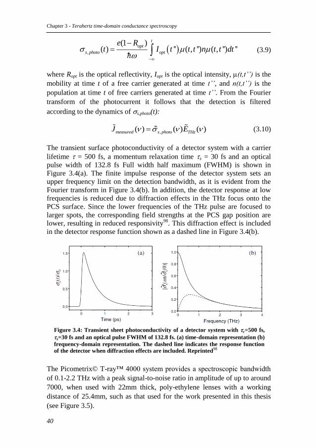
Chapter 3 - Terahertz time-domain conductance spectroscopy
40
,
(1 )( ) '' ( , '') ( , '') ''
topt
s photo opt
e Rt I t t t n t t dt
(3.9)
where Ropt is the optical reflectivity, Iopt is the optical intensity, (t,t’’) is the
mobility at time t of a free carrier generated at time t’’, and n(t,t’’) is the
population at time t of free carriers generated at time t’’. From the Fourier
transform of the photocurrent it follows that the detection is filtered
according to the dynamics of s,photo(t):
,( ) ( ) ( )measured s photo THzJ E (3.10)
The transient surface photoconductivity of a detector system with a carrier
lifetime = 500 fs, a momentum relaxation time s = 30 fs and an optical
pulse width of 132.8 fs Full width half maximum (FWHM) is shown in
Figure 3.4(a). The finite impulse response of the detector system sets an
upper frequency limit on the detection bandwidth, as it is evident from the
Fourier transform in Figure 3.4(b). In addition, the detector response at low
frequencies is reduced due to diffraction effects in the THz focus onto the
PCS surface. Since the lower frequencies of the THz pulse are focused to
larger spots, the corresponding field strengths at the PCS gap position are
lower, resulting in reduced responsivity98
. This diffraction effect is included
in the detector response function shown as a dashed line in Figure 3.4(b).
Figure 3.4: Transient sheet photoconductivity of a detector system with c=500 fs,
s=30 fs and an optical pulse FWHM of 132.8 fs. (a) time-domain representation (b)
frequency-domain representation. The dashed line indicates the response function
of the detector when diffraction effects are included. Reprinted98
The Picometrix© T-ray™ 4000 system provides a spectroscopic bandwidth
of 0.1-2.2 THz with a peak signal-to-noise ratio in amplitude of up to around
7000, when used with 22mm thick, poly-ethylene lenses with a working
distance of 25.4mm, such as that used for the work presented in this thesis
(see Figure 3.5).
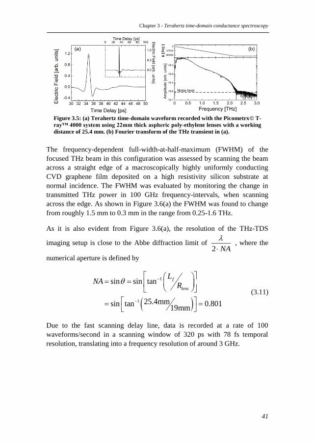
Chapter 3 - Terahertz time-domain conductance spectroscopy
41
Figure 3.5: (a) Terahertz time-domain waveform recorded with the Picometrx© T-
ray™ 4000 system using 22mm thick aspheric poly-ethylene lenses with a working
distance of 25.4 mm. (b) Fourier transform of the THz transient in (a).
The frequency-dependent full-width-at-half-maximum (FWHM) of the
focused THz beam in this configuration was assessed by scanning the beam
across a straight edge of a macroscopically highly uniformly conducting
CVD graphene film deposited on a high resistivity silicon substrate at
normal incidence. The FWHM was evaluated by monitoring the change in
transmitted THz power in 100 GHz frequency-intervals, when scanning
across the edge. As shown in Figure 3.6(a) the FWHM was found to change
from roughly 1.5 mm to 0.3 mm in the range from 0.25-1.6 THz.
As it is also evident from Figure 3.6(a), the resolution of the THz-TDS
imaging setup is close to the Abbe diffraction limit of 2 NA
, where the
numerical aperture is defined by
1
1
sin sin tan
25.4mm sin tan 0.80119mm
f
lens
LNA
R
(3.11)
Due to the fast scanning delay line, data is recorded at a rate of 100
waveforms/second in a scanning window of 320 ps with 78 fs temporal
resolution, translating into a frequency resolution of around 3 GHz.
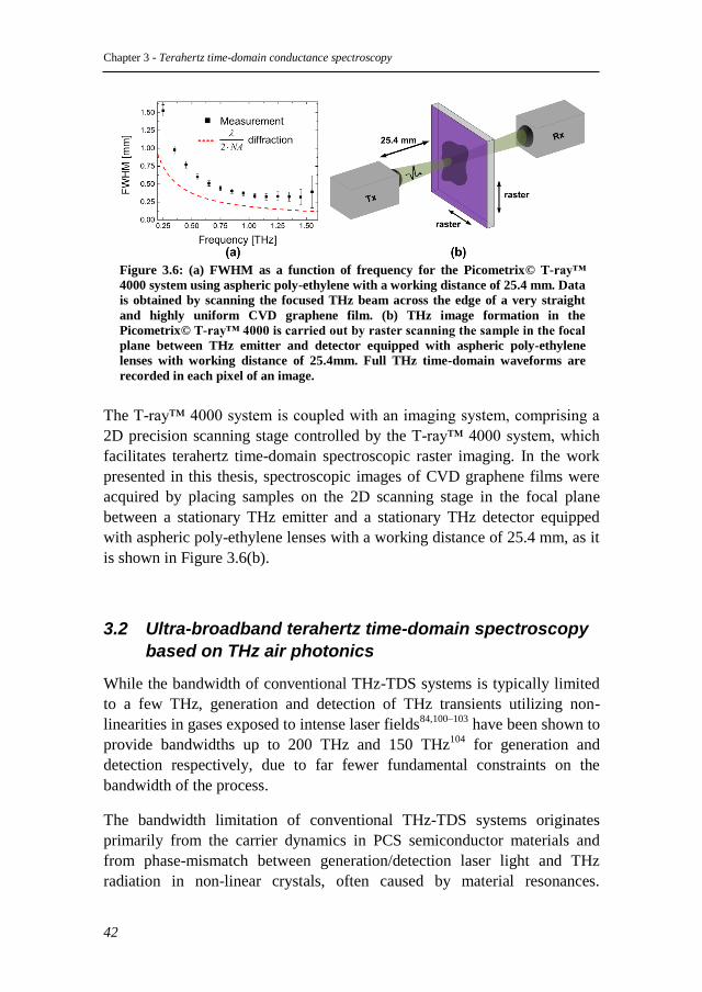
Chapter 3 - Terahertz time-domain conductance spectroscopy
42
Figure 3.6: (a) FWHM as a function of frequency for the Picometrix© T-ray™
4000 system using aspheric poly-ethylene with a working distance of 25.4 mm. Data
is obtained by scanning the focused THz beam across the edge of a very straight
and highly uniform CVD graphene film. (b) THz image formation in the
Picometrix© T-ray™ 4000 is carried out by raster scanning the sample in the focal
plane between THz emitter and detector equipped with aspheric poly-ethylene
lenses with working distance of 25.4mm. Full THz time-domain waveforms are
recorded in each pixel of an image.
The T-ray™ 4000 system is coupled with an imaging system, comprising a
2D precision scanning stage controlled by the T-ray™ 4000 system, which
facilitates terahertz time-domain spectroscopic raster imaging. In the work
presented in this thesis, spectroscopic images of CVD graphene films were
acquired by placing samples on the 2D scanning stage in the focal plane
between a stationary THz emitter and a stationary THz detector equipped
with aspheric poly-ethylene lenses with a working distance of 25.4 mm, as it
is shown in Figure 3.6(b).
3.2 Ultra-broadband terahertz time-domain spectroscopy
based on THz air photonics
While the bandwidth of conventional THz-TDS systems is typically limited
to a few THz, generation and detection of THz transients utilizing non-
linearities in gases exposed to intense laser fields84,100–103
have been shown to
provide bandwidths up to 200 THz and 150 THz104
for generation and
detection respectively, due to far fewer fundamental constraints on the
bandwidth of the process.
The bandwidth limitation of conventional THz-TDS systems originates
primarily from the carrier dynamics in PCS semiconductor materials and
from phase-mismatch between generation/detection laser light and THz
radiation in non-linear crystals, often caused by material resonances.
Chapter 3 - Terahertz time-domain conductance spectroscopy
43
Because dry air as well as nitrogen provides close to perfect phase-matching
across the entire electromagnetic spectrum and do not exhibit any absorption
resonances, THz-TDS based on generation and detection in air - coined
‘THz wave air photonics’85
– provide spectroscopic bandwidths that to a first
order is only limited by the fs laser pulse bandwidth. In addition the acquired
waveforms do not suffer from reflections in the detection media, which work
to limit the spectral resolution of other techniques. THz wave air photonics is
applied in this thesis to obtain usable bandwidth from 1-30 THz in free space
THz-TDS experiments.
3.2.1 THz pulse generation in a two-color laser-induced air
plasma
In recent years it has been shown that efficient free space THz transient
generation can be obtained from the formation of ultra-short laser induced
air plasma, by focusing of fs laser pulses with their second harmonic100,102,105
(SH). While a detailed understanding of the THz generation process requires
consideration of the electron trajectories106,107
and transient micro-
currents108,109
in the two-color air plasma as well as the influence of its finite
length on phase-matching between the fundamental and second-harmonic
beams110–113
, an approximation is offered by a four-wave mixing
description85,100,114
in the non-linear two-color air plasma environment
(3) * *
2THzE E E E (3.12)
where two fundamental photons, E*, are mixed with a SH photon, E2,
through the non-linear third-order susceptibility, (3)
, of the air plasma to
produce a THz photon. In terms of dependence on optical power the THz
field can thus be written as
(3)
2 cosTHzE I I (3.13)
where explicitly denotes the relative phase between fundamental and SH
wavelengths. Xie et al. showed that THz generation was most efficient when
fundamental, SH, and THz photons are all polarized along the same axis,
corresponding to the (3)
xxxx term of the third-order susceptibility102
.
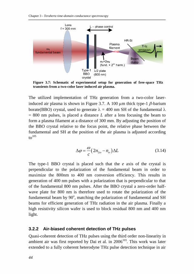
Chapter 3 - Terahertz time-domain conductance spectroscopy
44
Figure 3.7: Schematic of experimental setup for generation of free-space THz
transients from a two-color laser induced air plasma.
The utilized implementation of THz generation from a two-color laser-
induced air plasma is shown in Figure 3.7. A 100 m thick type-1 -barium
borate(BBO) crystal, used to generate = 400 nm SH of the fundamental
= 800 nm pulses, is placed a distance L after a lens focusing the beam to
form a plasma filament at a distance of 300 mm. By adjusting the position of
the BBO crystal relative to the focus point, the relative phase between the
fundamental and SH at the position of the air plasma is adjusted according
to105
22n n Lc
(3.14)
The type-1 BBO crystal is placed such that the e axis of the crystal is
perpendicular to the polarization of the fundamental beam in order to
maximize the 800nm to 400 nm conversion efficiency. This results in
generation of 400 nm pulses with a polarization that is perpendicular to that
of the fundamental 800 nm pulses. After the BBO crystal a zero-order half-
wave plate for 800 nm is therefore used to rotate the polarization of the
fundamental beam by 90o, matching the polarization of fundamental and SH
beams for efficient generation of THz radiation in the air plasma. Finally a
high resistivity silicon wafer is used to block residual 800 nm and 400 nm
light.
3.2.2 Air-biased coherent detection of THz pulses
Quasi-coherent detection of THz pulses using the third order non-linearity in
ambient air was first reported by Dai et al. in 2006103
. This work was later
extended to a fully coherent heterodyne THz pulse detection technique in air
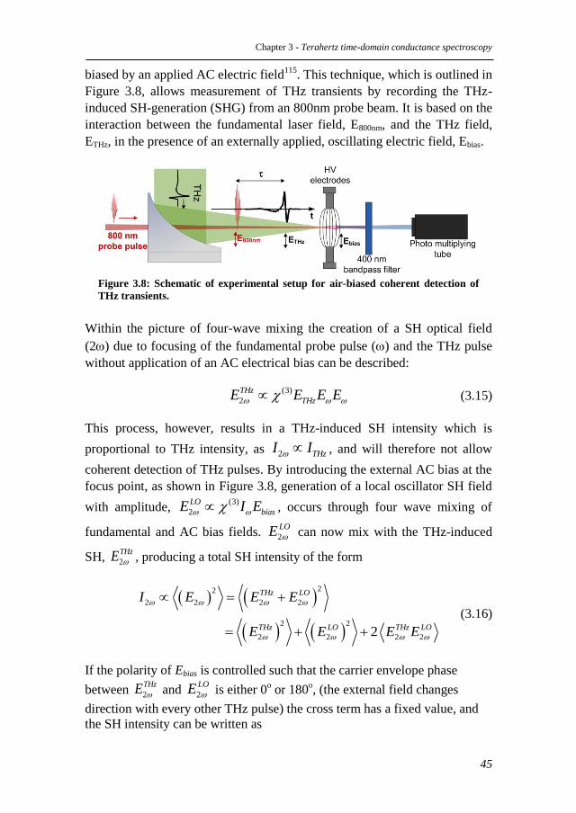
Chapter 3 - Terahertz time-domain conductance spectroscopy
45
biased by an applied AC electric field115
. This technique, which is outlined in
Figure 3.8, allows measurement of THz transients by recording the THz-
induced SH-generation (SHG) from an 800nm probe beam. It is based on the
interaction between the fundamental laser field, E800nm, and the THz field,
ETHz, in the presence of an externally applied, oscillating electric field, Ebias.
Figure 3.8: Schematic of experimental setup for air-biased coherent detection of
THz transients.
Within the picture of four-wave mixing the creation of a SH optical field
(2) due to focusing of the fundamental probe pulse () and the THz pulse
without application of an AC electrical bias can be described:
(3)
2
THz
THzE E E E (3.15)
This process, however, results in a THz-induced SH intensity which is
proportional to THz intensity, as 2 THzI I , and will therefore not allow
coherent detection of THz pulses. By introducing the external AC bias at the
focus point, as shown in Figure 3.8, generation of a local oscillator SH field
with amplitude, (3)
2
LO
biasE I E , occurs through four wave mixing of
fundamental and AC bias fields. 2
LOE can now mix with the THz-induced
SH, 2
THzE , producing a total SH intensity of the form
22
2 2 2 2
2 2
2 2 2 2 2
THz LO
THz LO THz LO
I E E E
E E E E
(3.16)
If the polarity of Ebias is controlled such that the carrier envelope phase
between 2
THzE and 2
LOE is either 0o or 180
o, (the external field changes
direction with every other THz pulse) the cross term has a fixed value, and
the SH intensity can be written as
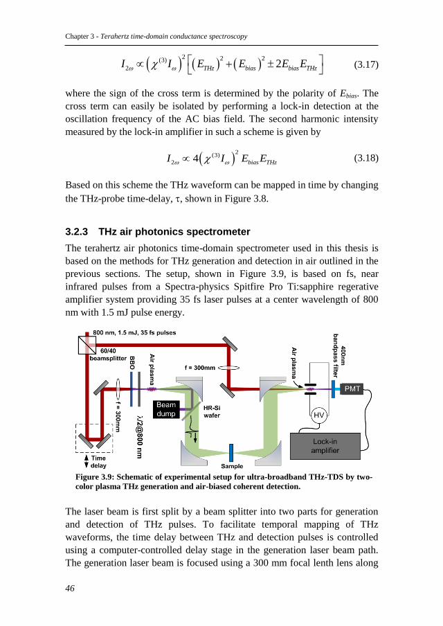
Chapter 3 - Terahertz time-domain conductance spectroscopy
46
2 2 2(3)
2 2THz bias bias THzI I E E E E
(3.17)
where the sign of the cross term is determined by the polarity of Ebias. The
cross term can easily be isolated by performing a lock-in detection at the
oscillation frequency of the AC bias field. The second harmonic intensity
measured by the lock-in amplifier in such a scheme is given by
2
(3)
2 4 bias THzI I E E (3.18)
Based on this scheme the THz waveform can be mapped in time by changing
the THz-probe time-delay, , shown in Figure 3.8.
3.2.3 THz air photonics spectrometer
The terahertz air photonics time-domain spectrometer used in this thesis is
based on the methods for THz generation and detection in air outlined in the
previous sections. The setup, shown in Figure 3.9, is based on fs, near
infrared pulses from a Spectra-physics Spitfire Pro Ti:sapphire regerative
amplifier system providing 35 fs laser pulses at a center wavelength of 800
nm with 1.5 mJ pulse energy.
Figure 3.9: Schematic of experimental setup for ultra-broadband THz-TDS by two-
color plasma THz generation and air-biased coherent detection.
The laser beam is first split by a beam splitter into two parts for generation
and detection of THz pulses. To facilitate temporal mapping of THz
waveforms, the time delay between THz and detection pulses is controlled
using a computer-controlled delay stage in the generation laser beam path.
The generation laser beam is focused using a 300 mm focal lenth lens along
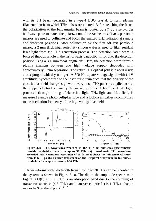
Chapter 3 - Terahertz time-domain conductance spectroscopy
47
with its SH beam, generated in a type-1 BBO crystal, to form plasma
filamentation from which THz pulses are emitted. Before reaching the focus,
the polarization of the fundamental beam is rotated by 90o by a zero-order
half wave plate to match the polarization of the SH beam. Off-axis parabolic
mirrors are used to collimate and focus the emitted THz radiation at sample
and detection positions. After collimation by the first off-axis parabolic
mirror, a 2 mm thick high resistivity silicon wafer is used to filter residual
laser light from the THz generation process. The detection laser beam is
focused through a hole in the last off-axis parabolic mirror onto the detection
position using a 300 mm focal length lens. Here, the detection beam forms a
plasma filament between two high voltage copper electrodes with
approximately 3 mm separation. The entire THz optical path is placed inside
a box purged with dry nitrogen. A 500 Hz square voltage signal with 6 kV
amplitude, synchronized to the laser pulse train such that the polarity of the
electric bias field changes sign with every other THz pulse, is applied across
the copper electrodes. Finally the intensity of the THz-induced SH light,
produced through mixing of detection light, THz light and bias field, is
measured using a photomultiplier tube and a lock-in amplifier synchronized
to the oscillation frequency of the high voltage bias field.
Figure 3.10: THz waveforms recorded in the THz air photonics spectrometer
provide bandwidth from 1 to up to 30 THz. (a) time-domain THz waveform
recorded with a temporal resolution of 10 fs. Inset shows the full temporal trace
from 0 to 3 ps (b) Fourier transform of the temporal waveform in (a) shows
bandwidth from approximately 1-30 THz
THz waveforms with bandwidth from 1 to up to 30 THz can be recorded in
the system as shown in Figure 3.10. The dip in the amplitude spectrum in
Figure 3.10(b) at 18.6 THz is an absorption band due to the coupling of
transverse acoustic (4.5 THz) and transverse optical (14.1 THz) phonon
modes in Si at the X point116,117
.

Chapter 3 - Terahertz time-domain conductance spectroscopy
48
3.2.4 Spectra-physics Spitfire Pro Ti:Sapphire regenerative
amplifier system
The Spectra-physics Spitfire Pro is a Ti:Sapphire regenerative amplifier
system providing fs laser pulses for THz air photonics spectroscopy. A
regenerative amplifier system produces high-power ultra-short laser pulses
by multiple passes of ultra-short seed pulses along with high-power pump
pulses in a gain medium inside a resonator cavity.
As indicated in Figure 3.11, the amplifier system consists of four main parts.
Two of these parts are the ‘Millennia Pro’ diode-pumped frequency doubled
solid-state pump laser delivering 4.2 W CW power and the ‘Tsunami’
Ti:Sapphire oscillator, which provides seed pulses with a duration of 25 fs,
bandwidth of 60 nm, pulse energy of approximately 5 nJ at a center
wavelength of 800 nm and a repetition rate of 76 MHz.
Figure 3.11: Spitfire Pro Ti:Sapphire regenerative amplifier system from Spectra-
physics. Reprinted118
The third part of the amplifier system is the ‘Empower’ pump laser which is
a diode-pumped, Q-switched Neodymium-doped yttrium lithium fluoride
(Nd:YLF) laser delivering frequency-doubled pump pulses with ns duration,
20 mJ pulses energy at = 527 nm and a repetition rate of 1 kHz. The fourth
part is the ‘Spitfire Pro’ regenerative amplifier comprising pulse stretching
and compression optics, Ti:Sapphire gain crystal and gain resonator, as well
as Pockel-cell-based optical switches for picking of synchronized seed and
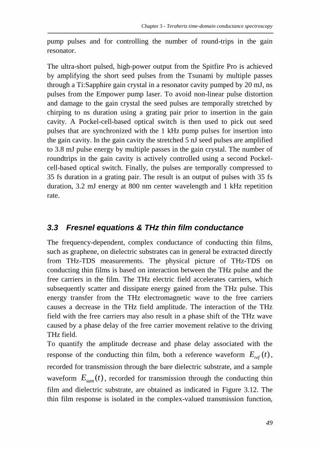
Chapter 3 - Terahertz time-domain conductance spectroscopy
49
pump pulses and for controlling the number of round-trips in the gain
resonator.
The ultra-short pulsed, high-power output from the Spitfire Pro is achieved
by amplifying the short seed pulses from the Tsunami by multiple passes
through a Ti:Sapphire gain crystal in a resonator cavity pumped by 20 mJ, ns
pulses from the Empower pump laser. To avoid non-linear pulse distortion
and damage to the gain crystal the seed pulses are temporally stretched by
chirping to ns duration using a grating pair prior to insertion in the gain
cavity. A Pockel-cell-based optical switch is then used to pick out seed
pulses that are synchronized with the 1 kHz pump pulses for insertion into
the gain cavity. In the gain cavity the stretched 5 nJ seed pulses are amplified
to 3.8 mJ pulse energy by multiple passes in the gain crystal. The number of
roundtrips in the gain cavity is actively controlled using a second Pockel-
cell-based optical switch. Finally, the pulses are temporally compressed to
35 fs duration in a grating pair. The result is an output of pulses with 35 fs
duration, 3.2 mJ energy at 800 nm center wavelength and 1 kHz repetition
rate.
3.3 Fresnel equations & THz thin film conductance
The frequency-dependent, complex conductance of conducting thin films,
such as graphene, on dielectric substrates can in general be extracted directly
from THz-TDS measurements. The physical picture of THz-TDS on
conducting thin films is based on interaction between the THz pulse and the
free carriers in the film. The THz electric field accelerates carriers, which
subsequently scatter and dissipate energy gained from the THz pulse. This
energy transfer from the THz electromagnetic wave to the free carriers
causes a decrease in the THz field amplitude. The interaction of the THz
field with the free carriers may also result in a phase shift of the THz wave
caused by a phase delay of the free carrier movement relative to the driving
THz field.
To quantify the amplitude decrease and phase delay associated with the
response of the conducting thin film, both a reference waveform ( )refE t ,
recorded for transmission through the bare dielectric substrate, and a sample
waveform ( )samE t , recorded for transmission through the conducting thin
film and dielectric substrate, are obtained as indicated in Figure 3.12. The
thin film response is isolated in the complex-valued transmission function,
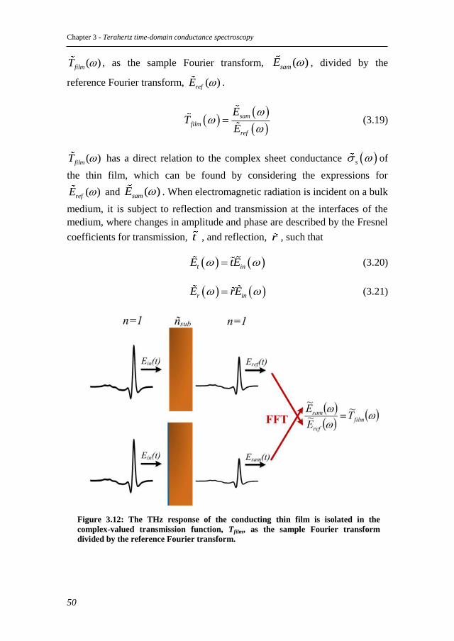
Chapter 3 - Terahertz time-domain conductance spectroscopy
50
( )filmT , as the sample Fourier transform, ( )samE , divided by the
reference Fourier transform, ( )refE .
sam
film
ref
ET
E
(3.19)
( )filmT has a direct relation to the complex sheet conductance s of
the thin film, which can be found by considering the expressions for
( )refE and ( )samE . When electromagnetic radiation is incident on a bulk
medium, it is subject to reflection and transmission at the interfaces of the
medium, where changes in amplitude and phase are described by the Fresnel
coefficients for transmission, t , and reflection, r , such that
t inE tE (3.20)
r inE rE (3.21)
Figure 3.12: The THz response of the conducting thin film is isolated in the
complex-valued transmission function, Tfilm, as the sample Fourier transform
divided by the reference Fourier transform.
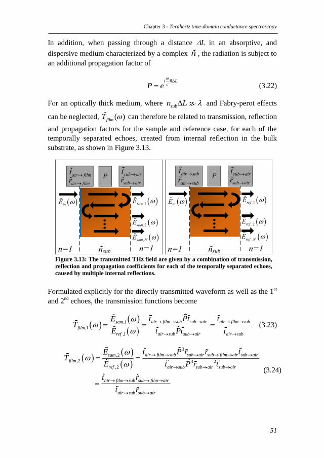
Chapter 3 - Terahertz time-domain conductance spectroscopy
51
In addition, when passing through a distance L in an absorptive, and
dispersive medium characterized by a complex n , the radiation is subject to
an additional propagation factor of
i n L
cP e
(3.22)
For an optically thick medium, where subn L and Fabry-perot effects
can be neglected, ( )filmT can therefore be related to transmission, reflection
and propagation factors for the sample and reference case, for each of the
temporally separated echoes, created from internal reflection in the bulk
substrate, as shown in Figure 3.13.
Figure 3.13: The transmitted THz field are given by a combination of transmission,
reflection and propagation coefficients for each of the temporally separated echoes,
caused by multiple internal reflections.
Formulated explicitly for the directly transmitted waveform as well as the 1st
and 2nd
echoes, the transmission functions become
,1
,1
,1
air film sub sub air air film subsam
film
ref air sub sub air air sub
t Pt tET
E t Pt t
(3.23)
3
,2
,2 3 2
,2
air film sub sub air sub film air sub airsam
film
ref air sub sub air sub air
air film sub sub film air
air sub sub air
t P r r tET
E t P r t
t r
t r
(3.24)
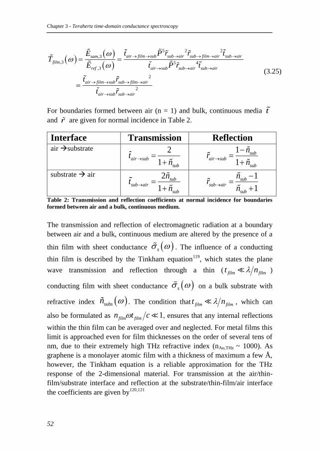
Chapter 3 - Terahertz time-domain conductance spectroscopy
52
5 2 2
,3
,3 5 4
,3
2
2
air film sub sub air sub film air sub airsam
film
ref air sub sub air sub air
air film sub sub film air
air sub sub air
t P r r tET
E t P r t
t r
t r
(3.25)
For boundaries formed between air (n = 1) and bulk, continuous media t
and r are given for normal incidence in Table 2.
Interface Transmission Reflection
air substrate 2
1air sub
sub
tn
1
1
subair sub
sub
nr
n
substrate air 2
1
subsub air
sub
nt
n
1
1
subsub air
sub
nr
n
Table 2: Transmission and reflection coefficients at normal incidence for boundaries
formed between air and a bulk, continuous medium.
The transmission and reflection of electromagnetic radiation at a boundary
between air and a bulk, continuous medium are altered by the presence of a
thin film with sheet conductance s . The influence of a conducting
thin film is described by the Tinkham equation119
, which states the plane
wave transmission and reflection through a thin ( film filmt n )
conducting film with sheet conductance s on a bulk substrate with
refractive index subsn . The condition that film filmt n , which can
also be formulated as 1film filmn t c ensures that any internal reflections
within the thin film can be averaged over and neglected. For metal films this
limit is approached even for film thicknesses on the order of several tens of
nm, due to their extremely high THz refractive index (nAu,THz ~ 1000). As
graphene is a monolayer atomic film with a thickness of maximum a few Å,
however, the Tinkham equation is a reliable approximation for the THz
response of the 2-dimensional material. For transmission at the air/thin-
film/substrate interface and reflection at the substrate/thin-film/air interface
the coefficients are given by120,121
Chapter 3 - Terahertz time-domain conductance spectroscopy
53
0
2
1air film sub
sub s
tn Z
(3.26)
0
0
1,
1
sub s
sub film air
sub s
n Zr
n Z
(3.27)
where Z0 = 377 is the vacuum impedance. Combining equations (3.23),
(3.24), (3.25), (3.26), (3.27) and expressions in Table 2, the relation between
thin film sheet conductance, s , and complex transmission function,
( )filmT , can be explicitly written for the directly transmitted THz fields as
well as the 1st echo as
,1
,1
,1 0
1
1
sam subfilm
ref sub s
E nT
E n Z
(3.28)
2
0,2
,2 2
,2 0
1 1.
1 1
sub s subsam
film
ref sub s sub
n Z nET
E n Z n
(3.29)
This results in analytical expressions for the thin film sheet conductance
,1
0
1 As A
film
nn
Z T
(3.30)
2 2 2
,2
0
4 2,
2
A A A B film A A B film
s
B film
n n n n T n n n T
n Z T
(3.31)
where 1A subn n and 1B subn n .
Chapter 3 - Terahertz time-domain conductance spectroscopy
54
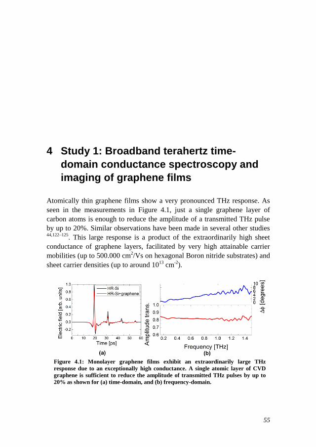
55
4 Study 1: Broadband terahertz time-
domain conductance spectroscopy and
imaging of graphene films
Atomically thin graphene films show a very pronounced THz response. As
seen in the measurements in Figure 4.1, just a single graphene layer of
carbon atoms is enough to reduce the amplitude of a transmitted THz pulse
by up to 20%. Similar observations have been made in several other studies 44,122–125
. This large response is a product of the extraordinarily high sheet
conductance of graphene layers, facilitated by very high attainable carrier
mobilities (up to 500.000 cm2/Vs on hexagonal Boron nitride substrates) and
sheet carrier densities (up to around 1013
cm-2
).
Figure 4.1: Monolayer graphene films exhibit an extraordinarily large THz
response due to an exceptionally high conductance. A single atomic layer of CVD
graphene is sufficient to reduce the amplitude of transmitted THz pulses by up to
20% as shown for (a) time-domain, and (b) frequency-domain.
Chapter 4 – Study 1: Broadband terahertz time-domain conductance spectroscopy and imaging…
56
Several Fourier transform infrared spectroscopy (FTIR)44,122,123,126,127
and
THz-TDS124,127
investigations have shown that the frequency dependent
optical absorption at THz to mid-infrared frequencies generally follows a
Drude model. These observations agree with THz-TDS measurements on
epitaxial122,123
and CVD121,125,128,129
graphene that has shown spectrally
predominantly flat THz responses in the range from 0.15-2.0 THz, consistent
with a Drude conductance response and carrier scattering rates that are
significantly higher than the measurable frequencies ( 2 f ). As will
be shown later in this chapter, however, a seemingly spectrally flat
conductance at low THz frequencies can also reflect non-Drude behavior
such as e.g. Drude-smith.
In consistency with most theoretical work on graphene, prior studies indicate
that the electrodynamic response of graphene in the THz range at low field
strengths (< 1 kV/cm) is dominated by intraband processes reflecting the AC
electrical conduction properties of the film.
In this chapter the THz response of graphene grown by CVD on single-
crystalline (S-C) Cu (111) as well as poly-crystalline (poly-C) Cu foil is
characterized from 0.15-1.5 by THz-TDS THz based on generation and
detection in photoconductive switches and from 1-15 THz by THz-TDS
based on THz wave air photonics. We show that both amplitude and phase
of the THz response is in one case well described by a Drude model and in
the other case by a Drude-Smith model for intraband conductivity. Despite
of the qualitative difference between THz conductance properties of the two
films, these observations testify that the carrier transport in both films is
diffusive in nature. By comparison to micro four-point probe measurements
we experimentally confirm that the conductance measured by THz-TDS in
the low frequency limit ( 2 f ) of the Drude spectrum for an
electrically continuous graphene film reflects the graphene DC conductance.
This observation opens up the possibility of utilization of THz-TDS as rapid,
quantitative and contact-free metrology tool for mapping of the nanoscopic
conductance of large-area graphene, suitable for in-line electrical
characterization in industrial settings. Finally, a demonstration of wafer-
scale graphene conductance mapping is presented using terahertz time-
domain spectroscopic imaging of CVD graphene.
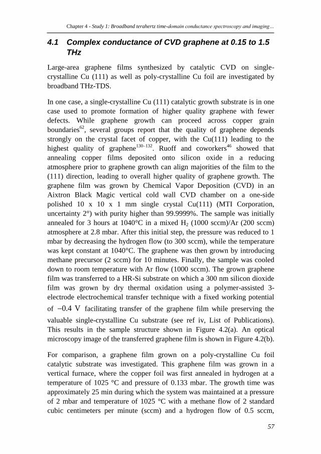
Chapter 4 - Study 1: Broadband terahertz time-domain conductance spectroscopy and imaging…
57
4.1 Complex conductance of CVD graphene at 0.15 to 1.5
THz
Large-area graphene films synthesized by catalytic CVD on single-
crystalline Cu (111) as well as poly-crystalline Cu foil are investigated by
broadband THz-TDS.
In one case, a single-crystalline Cu (111) catalytic growth substrate is in one
case used to promote formation of higher quality graphene with fewer
defects. While graphene growth can proceed across copper grain
boundaries62
, several groups report that the quality of graphene depends
strongly on the crystal facet of copper, with the Cu(111) leading to the
highest quality of graphene130–132
. Ruoff and coworkers46
showed that
annealing copper films deposited onto silicon oxide in a reducing
atmosphere prior to graphene growth can align majorities of the film to the
(111) direction, leading to overall higher quality of graphene growth. The
graphene film was grown by Chemical Vapor Deposition (CVD) in an
Aixtron Black Magic vertical cold wall CVD chamber on a one-side
polished 10 x 10 x 1 mm single crystal Cu(111) (MTI Corporation,
uncertainty 2°) with purity higher than 99.9999%. The sample was initially
annealed for 3 hours at 1040°C in a mixed H2 (1000 sccm)/Ar (200 sccm)
atmosphere at 2.8 mbar. After this initial step, the pressure was reduced to 1
mbar by decreasing the hydrogen flow (to 300 sccm), while the temperature
was kept constant at 1040°C. The graphene was then grown by introducing
methane precursor (2 sccm) for 10 minutes. Finally, the sample was cooled
down to room temperature with Ar flow (1000 sccm). The grown graphene
film was transferred to a HR-Si substrate on which a 300 nm silicon dioxide
film was grown by dry thermal oxidation using a polymer-assisted 3-
electrode electrochemical transfer technique with a fixed working potential
of 0.4 V facilitating transfer of the graphene film while preserving the
valuable single-crystalline Cu substrate (see ref iv, List of Publications).
This results in the sample structure shown in Figure 4.2(a). An optical
microscopy image of the transferred graphene film is shown in Figure 4.2(b).
For comparison, a graphene film grown on a poly-crystalline Cu foil
catalytic substrate was investigated. This graphene film was grown in a
vertical furnace, where the copper foil was first annealed in hydrogen at a
temperature of 1025 °C and pressure of 0.133 mbar. The growth time was
approximately 25 min during which the system was maintained at a pressure
of 2 mbar and temperature of 1025 °C with a methane flow of 2 standard
cubic centimeters per minute (sccm) and a hydrogen flow of 0.5 sccm,
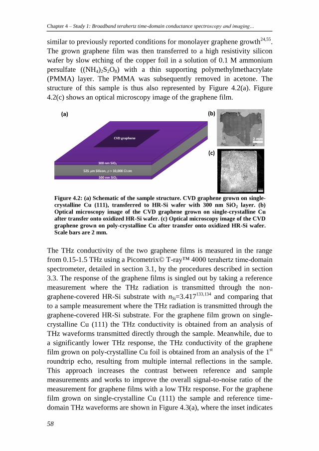
Chapter 4 – Study 1: Broadband terahertz time-domain conductance spectroscopy and imaging…
58
similar to previously reported conditions for monolayer graphene growth24,55
.
The grown graphene film was then transferred to a high resistivity silicon
wafer by slow etching of the copper foil in a solution of 0.1 M ammonium
persulfate ((NH4)2S2O8) with a thin supporting polymethylmethacrylate
(PMMA) layer. The PMMA was subsequently removed in acetone. The
structure of this sample is thus also represented by Figure 4.2(a). Figure
4.2(c) shows an optical microscopy image of the graphene film.
Figure 4.2: (a) Schematic of the sample structure. CVD graphene grown on single-
crystalline Cu (111), transferred to HR-Si wafer with 300 nm SiO2 layer. (b)
Optical microscopy image of the CVD graphene grown on single-crystalline Cu
after transfer onto oxidized HR-Si wafer. (c) Optical microscopy image of the CVD
graphene grown on poly-crystalline Cu after transfer onto oxidized HR-Si wafer.
Scale bars are 2 mm.
The THz conductivity of the two graphene films is measured in the range
from 0.15-1.5 THz using a Picometrix© T-ray™ 4000 terahertz time-domain
spectrometer, detailed in section 3.1, by the procedures described in section
3.3. The response of the graphene films is singled out by taking a reference
measurement where the THz radiation is transmitted through the non-
graphene-covered HR-Si substrate with nSi=3.417133,134
and comparing that
to a sample measurement where the THz radiation is transmitted through the
graphene-covered HR-Si substrate. For the graphene film grown on single-
crystalline Cu (111) the THz conductivity is obtained from an analysis of
THz waveforms transmitted directly through the sample. Meanwhile, due to
a significantly lower THz response, the THz conductivity of the graphene
film grown on poly-crystalline Cu foil is obtained from an analysis of the 1st
roundtrip echo, resulting from multiple internal reflections in the sample.
This approach increases the contrast between reference and sample
measurements and works to improve the overall signal-to-noise ratio of the
measurement for graphene films with a low THz response. For the graphene
film grown on single-crystalline Cu (111) the sample and reference time-
domain THz waveforms are shown in Figure 4.3(a), where the inset indicates
Chapter 4 - Study 1: Broadband terahertz time-domain conductance spectroscopy and imaging…
59
the 20 ps duration of the Fermi-filtered time-windowing that has been
applied around the first peak to the full 320 ps time trace recorded in the
measurement. Similarly, Figure 4.3(b) shows sample and reference time-
domain THz waveforms for the graphene film grown on poly-crystalline Cu
foil, where the inset indicates the 10 ps time-window that was applied
around the second peak. The time-window in Figure 4.3(b) is narrower in
order to supress features related to the directly transmitted waveform.
Figure 4.3: Sample and reference THz time-domain waveforms for CVD graphene
films grown on (a) single-crystalline Cu (111) substrate (b) poly-crystalline Cu foil.
Resulting sheet conductance spectra for (c) single-crystalline Cu (111) substrate
(d) poly-crystalline Cu foil.
By analysing the complex Fourier transforms of the time-domain waveforms
in Figure 4.3(a) and Figure 4.3(b) according to the procedures outlined in
section 3.3, the complex, frequency-dependent sheet conductance, s , of the
two graphene films could be extracted, resulting in the spectra shown in
Figure 4.3(c) and Figure 4.3(d). The time-domain measurement for the S-C
Cu (111) graphene film in Figure 4.3(a) is an average of 10 recorded time
traces, while the corresponding measurement for the poly-C Cu foil
graphene film in Figure 4.3(b) is an average of 250 recorded time traces.
This results in a wider usable spectroscopic bandwidth of 0.15 to 1.5 THz for
the poly-C Cu foil graphene data, compared to 0.15 to 1.0 THz for the S-C
Cu (111) graphene data.
Chapter 4 – Study 1: Broadband terahertz time-domain conductance spectroscopy and imaging…
60
The conductance spectrum observed for the S-C Cu (111) graphene film
shows a real part of the conductance, 1, that is slowly decreasing with
frequency and an imaginary part of the conductance, 2, that slowly
increases with frequency. This type of conductance spectrum is consistent
with the response of a Drude conductor, which is apparent from the good fit
to the Drude model with DC = 2.19 mS and = 76 fs, shown in Figure
4.3(c). The conductance spectrum that we observe for the poly-C Cu foil
graphene film in contrast shows 1 and 2 that are predominantly flat and
constant at values of around 0.73 mS and 0, respectively, in the accessible
frequency range. Such a frequency dependent conductivity, s , can also be
described by the Drude model with a scattering rate that is much higher than
the accessible frequencies. As a consequence of the very flat spectrum,
however, a finite Drude scattering time cannot be inferred from the data
obtained for the poly-C Cu foil graphene film, reflecting that the accessible
frequency range is much lower than the scattering rate in the graphene film (
2 f ).
The sheet conductance spectra resulting from the THz-TDS investigation
presented here thus strongly indicate that carrier transport in the two CVD
graphene films is diffusive and well described within a Drude-type
framework, confirming the observations made in other, similar studies of
graphene. Based on a Hall mobilities of 2733 61cm VsH and
2333 30cm VsH for the S-C Cu and poly-C Cu films, respectively,
measured using the micro four-point probe Hall effect method135
, an
estimated typical Fermi level EF for CVD graphene of –0.4 eV, and the
observation of diffusive Drude-type transport in the graphene film, the
carrier diffusivity can be estimated as136
2
2147 cm s,
2 2
F s F
s
E ED
n e e
(4.1)
and
2
266 cm s,
2 2
F s F
s
E ED
n e e
(4.2)
for the two graphene films. The carrier diffusivity allows us to also estimate
the characteristic carrier transport length, L, associated with the THz-TDS
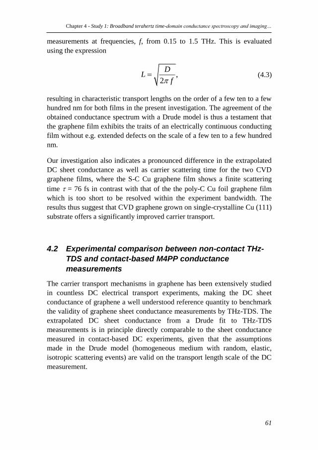
Chapter 4 - Study 1: Broadband terahertz time-domain conductance spectroscopy and imaging…
61
measurements at frequencies, f, from 0.15 to 1.5 THz. This is evaluated
using the expression
,2
DL
f (4.3)
resulting in characteristic transport lengths on the order of a few ten to a few
hundred nm for both films in the present investigation. The agreement of the
obtained conductance spectrum with a Drude model is thus a testament that
the graphene film exhibits the traits of an electrically continuous conducting
film without e.g. extended defects on the scale of a few ten to a few hundred
nm.
Our investigation also indicates a pronounced difference in the extrapolated
DC sheet conductance as well as carrier scattering time for the two CVD
graphene films, where the S-C Cu graphene film shows a finite scattering
time = 76 fs in contrast with that of the the poly-C Cu foil graphene film
which is too short to be resolved within the experiment bandwidth. The
results thus suggest that CVD graphene grown on single-crystalline Cu (111)
substrate offers a significantly improved carrier transport.
4.2 Experimental comparison between non-contact THz-
TDS and contact-based M4PP conductance
measurements
The carrier transport mechanisms in graphene has been extensively studied
in countless DC electrical transport experiments, making the DC sheet
conductance of graphene a well understood reference quantity to benchmark
the validity of graphene sheet conductance measurements by THz-TDS. The
extrapolated DC sheet conductance from a Drude fit to THz-TDS
measurements is in principle directly comparable to the sheet conductance
measured in contact-based DC experiments, given that the assumptions
made in the Drude model (homogeneous medium with random, elastic,
isotropic scattering events) are valid on the transport length scale of the DC
measurement.
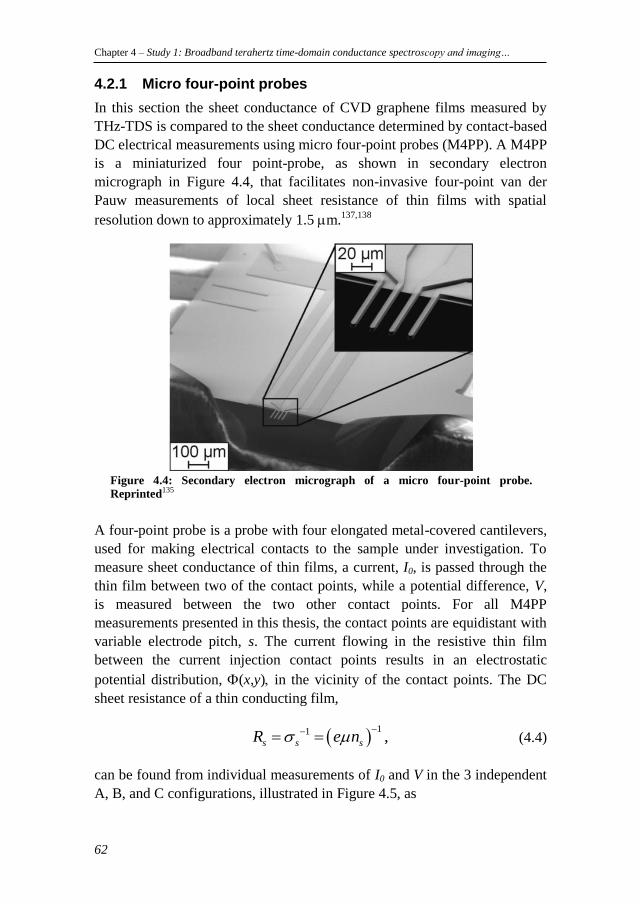
Chapter 4 – Study 1: Broadband terahertz time-domain conductance spectroscopy and imaging…
62
4.2.1 Micro four-point probes
In this section the sheet conductance of CVD graphene films measured by
THz-TDS is compared to the sheet conductance determined by contact-based
DC electrical measurements using micro four-point probes (M4PP). A M4PP
is a miniaturized four point-probe, as shown in secondary electron
micrograph in Figure 4.4, that facilitates non-invasive four-point van der
Pauw measurements of local sheet resistance of thin films with spatial
resolution down to approximately 1.5 m.137,138
Figure 4.4: Secondary electron micrograph of a micro four-point probe.
Reprinted135
A four-point probe is a probe with four elongated metal-covered cantilevers,
used for making electrical contacts to the sample under investigation. To
measure sheet conductance of thin films, a current, I0, is passed through the
thin film between two of the contact points, while a potential difference, V,
is measured between the two other contact points. For all M4PP
measurements presented in this thesis, the contact points are equidistant with
variable electrode pitch, s. The current flowing in the resistive thin film
between the current injection contact points results in an electrostatic
potential distribution, (x,y) in the vicinity of the contact points. The DC
sheet resistance of a thin conducting film,
11 ,s s sR e n (4.4)
can be found from individual measurements of I0 and V in the 3 independent
A, B, and C configurations, illustrated in Figure 4.5, as
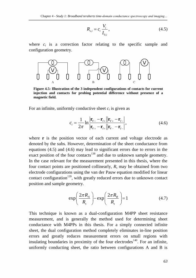
Chapter 4 - Study 1: Broadband terahertz time-domain conductance spectroscopy and imaging…
63
,
0,
,is i i
i
VR c
I (4.5)
where ci is a correction factor relating to the specific sample and
configuration geometry.
Figure 4.5: Illustration of the 3 independent configurations of contacts for current
injection and contacts for probing potential difference without presence of a
magnetic field.
For an infinite, uniformly conductive sheet ci is given as
1
ln ,2
V I V I
i
V I V I
c
r r r r
r r r r (4.6)
where r is the position vector of each current and voltage electrode as
denoted by the subs. However, determination of the sheet conductance from
equations (4.5) and (4.6) may lead to significant errors due to errors in the
exact position of the four contacts138
and due to unknown sample geometry.
In the case relevant for the measurement presented in this thesis, where the
four contact points are positioned collinearly, Rs may be obtained from two
electrode configurations using the van der Pauw equation modified for linear
contact configuration139
, with greatly reduced errors due to unknown contact
position and sample geometry.
2 2
exp exp 1A B
s s
R R
R R
(4.7)
This technique is known as a dual-configuration M4PP sheet resistance
measurement, and is generally the method used for determining sheet
conductance with M4PPs in this thesis. For a simply connected infinite
sheet, the dual configuration method completely eliminates in-line position
errors and greatly reduces measurement errors on small regions with
insulating boundaries in proximity of the four electrodes140
. For an infinite,
uniformly conducting sheet, the ratio between configurations A and B is
Chapter 4 – Study 1: Broadband terahertz time-domain conductance spectroscopy and imaging…
64
nominally 1.26, as indicated in Figure 4.6, which shows an example of data
recorded in a single dual configuration measurement.
Figure 4.6: Example of the measurement outcome in a dual configuration M4PP
sheet resistance measurement. As indicated, the ratio between resistances obtained
in the A and B configurations is nominally 1.26 for an infinite, uniformly
conducting sheet.
4.2.2 THz-TDS vs M4PP conductance: S-C Cu (111) graphene
film
The sheet conductance of the CVD graphene film grown on single-
crystalline Cu (111) was mapped by THz-TDS and dual configuration M4PP
sheet resistance line scan measurement in 200 m and in 50 m steps,
respectively, along the dashed line in Figure 4.7(a). The THz sheet
conductance values are evaluated as the average real part of the conductance
from 0.7 to 0.8 THz, a frequency range which was chosen to obtain the best
compromise between a reasonably good spatial resolution of 400 m and
sheet conductance values reasonably close to the DC-extrapolated value. A
single reference waveform recorded in a non-graphene-covered area of the
HR-Si substrate is used for the evaluation in all positions. For the M4PP line
scan, a 12 point-probe with 3 equidistant M4PP configurations of 4, 8 and 12
m probe pitch as well as 2 equidistant four point-probes with probe pitches
of 50 mm and 100 mm, were used to measure the DC sheet conductance at 5
transport lengths. For the THz-TDS conductance measurements the sample
was scanned relative to a stationary THz focus, while the M4PPs were
moved relative to the stationary sample to form the sheet conductance line
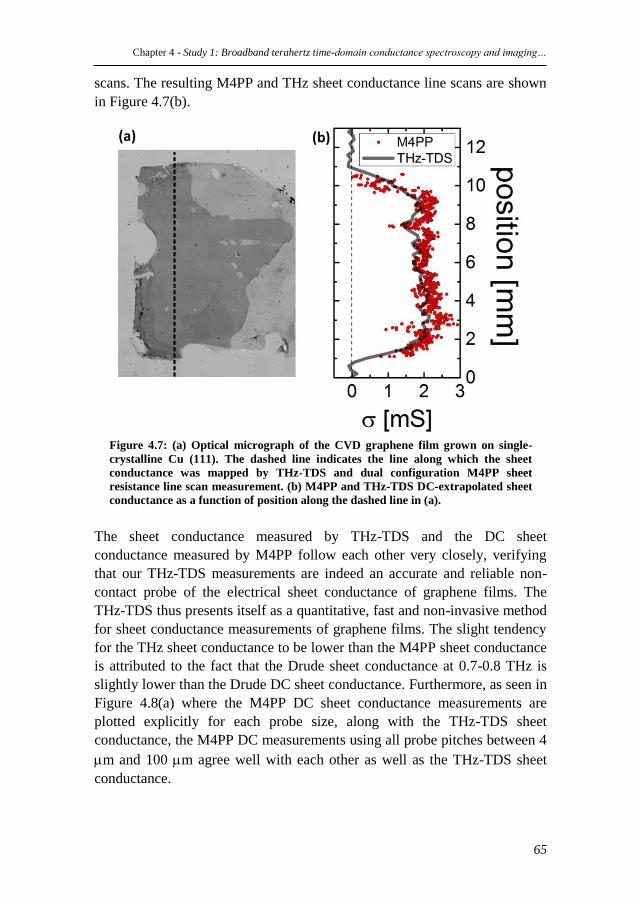
Chapter 4 - Study 1: Broadband terahertz time-domain conductance spectroscopy and imaging…
65
scans. The resulting M4PP and THz sheet conductance line scans are shown
in Figure 4.7(b).
Figure 4.7: (a) Optical micrograph of the CVD graphene film grown on single-
crystalline Cu (111). The dashed line indicates the line along which the sheet
conductance was mapped by THz-TDS and dual configuration M4PP sheet
resistance line scan measurement. (b) M4PP and THz-TDS DC-extrapolated sheet
conductance as a function of position along the dashed line in (a).
The sheet conductance measured by THz-TDS and the DC sheet
conductance measured by M4PP follow each other very closely, verifying
that our THz-TDS measurements are indeed an accurate and reliable non-
contact probe of the electrical sheet conductance of graphene films. The
THz-TDS thus presents itself as a quantitative, fast and non-invasive method
for sheet conductance measurements of graphene films. The slight tendency
for the THz sheet conductance to be lower than the M4PP sheet conductance
is attributed to the fact that the Drude sheet conductance at 0.7-0.8 THz is
slightly lower than the Drude DC sheet conductance. Furthermore, as seen in
Figure 4.8(a) where the M4PP DC sheet conductance measurements are
plotted explicitly for each probe size, along with the THz-TDS sheet
conductance, the M4PP DC measurements using all probe pitches between 4
m and 100 m agree well with each other as well as the THz-TDS sheet
conductance.
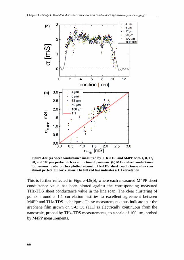
Chapter 4 – Study 1: Broadband terahertz time-domain conductance spectroscopy and imaging…
66
Figure 4.8: (a) Sheet conductance measured by THz-TDS and M4PP with 4, 8, 12,
50, and 100 m probe pitch as a function of positions. (b) M4PP sheet conductance
for various probe pitches plotted against THz-TDS sheet conductance shows an
almost perfect 1:1 correlation. The full red line indicates a 1:1 correlation
This is further reflected in Figure 4.8(b), where each measured M4PP sheet
conductance value has been plotted against the corresponding measured
THz-TDS sheet conductance value in the line scan. The clear clustering of
points around a 1:1 correlation testifies to excellent agreement between
M4PP and THz-TDS techniques. These measurements thus indicate that the
graphene film grown on S-C Cu (111) is electrically continuous from the
nanoscale, probed by THz-TDS measurements, to a scale of 100 m, probed
by M4PP measurements.
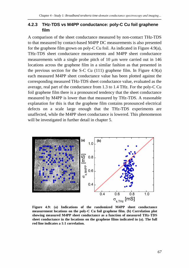
Chapter 4 - Study 1: Broadband terahertz time-domain conductance spectroscopy and imaging…
67
4.2.3 THz-TDS vs M4PP conductance: poly-C Cu foil graphene
film
A comparison of the sheet conductance measured by non-contact THz-TDS
to that measured by contact-based M4PP DC measurements is also presented
for the graphene film grown on poly-C Cu foil. As indicated in Figure 4.9(a),
THz-TDS sheet conductance measurements and M4PP sheet conductance
measurements with a single probe pitch of 10 m were carried out in 146
locations across the graphene film in a similar fashion as that presented in
the previous section for the S-C Cu (111) graphene film. In Figure 4.9(a)
each measured M4PP sheet conductance value has been plotted against the
corresponding measured THz-TDS sheet conductance value, evaluated as the
average, real part of the conductance from 1.3 to 1.4 THz. For the poly-C Cu
foil graphene film there is a pronounced tendency that the sheet conductance
measured by M4PP is lower than that measured by THz-TDS. A reasonable
explanation for this is that the graphene film contains pronounced electrical
defects on a scale large enough that the THz-TDS experiments are
unaffected, while the M4PP sheet conductance is lowered. This phenomenon
will be investigated in further detail in chapter 5.
Figure 4.9: (a) Indications of the randomized M4PP sheet conductance
measurement locations on the poly-C Cu foil graphene film. (b) Correlation plot
showing measured M4PP sheet conductance as a function of measured THz-TDS
sheet conductance in the locations on the graphene films indicated in (a). The full
red line indicates a 1:1 correlation.
Chapter 4 – Study 1: Broadband terahertz time-domain conductance spectroscopy and imaging…
68
4.3 Carrier nano-localization and preferential back-
scattering: Ultra-broadband THz conductance
spectroscopy of CVD graphene at 1 to 15 THz
Ultra-broadband THz-TDS based on THz air photonics facilitates accurate
experimental determination of the frequency-dependence of both real and
imaginary parts of the conductance of graphene films over a wide frequency
range. Due to a usable bandwidth of up to 15 THz obtained in the coherent
THz-TDS measurements presented here, we are able to resolve real and
imaginary parts of close to the entire frequency range associated with
intraband optical conductivity of the investigated graphene films.
The CVD graphene samples investigated in sections 4.1 and 4.2 were
characterized by ultra-broadband THz air photonics THz-TDS using the
experimental setup described in section 3.2. The response of the graphene
films is separated from that of the underlying HR-Si substrates by
performing sample and reference measurements in graphene-covered and
non-graphene-covered areas, respectively. Similar to the THz-TDS
investigation in section 4.1, the response of the graphene film grown on
single-crystalline Cu (111) is obtained from the directly transmitted THz
waveform, while the response of the graphene film grown on poly-
crystalline Cu foil is obtained from the 1st roundtrip echo, resulting from
multiple internal reflections in the sample. Measuring and analysing the 1st
echo increases the contrast between reference and sample measurements and
works to improve the overall signal-to-noise ratio of the measurement for
graphene films with a low THz response. At multi-THz frequencies, the
phase change due to slight variations in the thickness of the HR-Si from
sample position to reference position can be significant compared to the
phase change induced by the graphene film. As shown in Figure 4.10, it was
found that the substrate thickness of a 1 mm thick HR-Si wafer in extreme
cases can vary by more than 10 m across an area of 11.4x11.4 mm2. The
HR-Si thickness in Figure 4.10 was obtained through a fitting routine to the
THz waveform in each pixel. In this approach, an input THz time-domain
waveform, inE , is first measured with no sample in the THz-TD
spectrometer. The Fourier transform, inE , is computed, from which the
directly transmitted pulse and 1st, 2
nd, 3
rd and 4
th echoes are evaluated by the
relations
1 in air sub sub airE E t Pt (4.8)
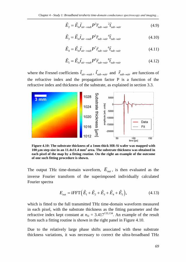
Chapter 4 - Study 1: Broadband terahertz time-domain conductance spectroscopy and imaging…
69
3 2
2 in air sub sub air sub airE E t P r t (4.9)
5 4
3 in air sub sub air sub airE E t P r t (4.10)
7 6
4 in air sub sub air sub airE E t P r t (4.11)
9 8
5 in air sub sub air sub airE E t P r t (4.12)
where the Fresnel coefficients air subt , sub airt and sub airr are functions of
the refractive index and the propagation factor P is a function of the
refractive index and thickness of the substrate, as explained in section 3.3.
Figure 4.10: The substrate thickness of a 1mm thick HR-Si wafer was mapped with
100 m step size in an 11.4x11.4 mm2 area. The substrate thickness was obtained in
each pixel of the map by a fitting routine. On the right an example of the outcome
of one such fitting procedure is shown.
The output THz time-domain waveform, outE , is then evaluated as the
inverse Fourier transform of the superimposed individually calculated
Fourier spectra
1 2 3 4 5iFFT ,outE E E E E E (4.13)
which is fitted to the full transmitted THz time-domain waveform measured
in each pixel, with the substrate thickness as the fitting parameter and the
refractive index kept constant at nSi = 3.417133,134
. An example of the result
from such a fitting routine is shown in the right panel in Figure 4.10.
Due to the relatively large phase shifts associated with these substrate
thickness variations, it was necessary to correct the ultra-broadband THz
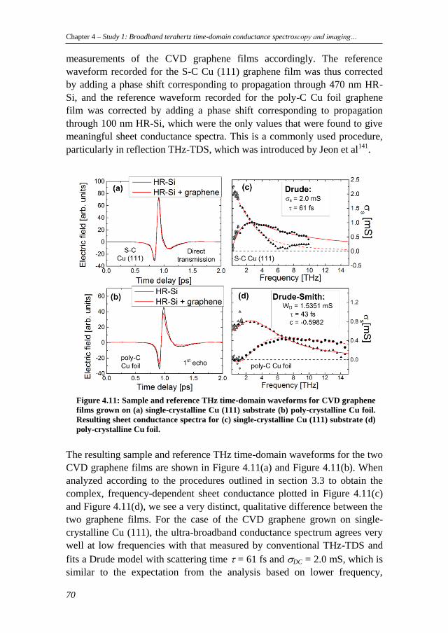
Chapter 4 – Study 1: Broadband terahertz time-domain conductance spectroscopy and imaging…
70
measurements of the CVD graphene films accordingly. The reference
waveform recorded for the S-C Cu (111) graphene film was thus corrected
by adding a phase shift corresponding to propagation through 470 nm HR-
Si, and the reference waveform recorded for the poly-C Cu foil graphene
film was corrected by adding a phase shift corresponding to propagation
through 100 nm HR-Si, which were the only values that were found to give
meaningful sheet conductance spectra. This is a commonly used procedure,
particularly in reflection THz-TDS, which was introduced by Jeon et al141
.
Figure 4.11: Sample and reference THz time-domain waveforms for CVD graphene
films grown on (a) single-crystalline Cu (111) substrate (b) poly-crystalline Cu foil.
Resulting sheet conductance spectra for (c) single-crystalline Cu (111) substrate (d)
poly-crystalline Cu foil.
The resulting sample and reference THz time-domain waveforms for the two
CVD graphene films are shown in Figure 4.11(a) and Figure 4.11(b). When
analyzed according to the procedures outlined in section 3.3 to obtain the
complex, frequency-dependent sheet conductance plotted in Figure 4.11(c)
and Figure 4.11(d), we see a very distinct, qualitative difference between the
two graphene films. For the case of the CVD graphene grown on single-
crystalline Cu (111), the ultra-broadband conductance spectrum agrees very
well at low frequencies with that measured by conventional THz-TDS and
fits a Drude model with scattering time = 61 fs and DC = 2.0 mS, which is
similar to the expectation from the analysis based on lower frequency,
Chapter 4 - Study 1: Broadband terahertz time-domain conductance spectroscopy and imaging…
71
conventional THz-TDS. Under an assumption of a Fermi velocity of vF = 106
m/s, the measured carrier scattering time translates to a mean free path of
6 1510 m s 61 10 s 61 nm,mfp Fl v (4.14)
It should be noted that although the graphene Fermi velocity is widely
accepted to be close to 106 m/s, recent studies have shown that vF can in
certain circumstances differ significantly from this value142
.
Under assumption of carrier transport dominated by long-range charged
impurity scattering, the carrier density can subsequently be obtained from
the measured DC = 2.0 mS as described in section 0.
2212 -2
4 2 25.7 10 cm ,DC
F
ne v
(4.15)
using a Fermi velocity 610 m s Fv .
In addition, the carrier mobility of the film can subsequently be evaluated as
also described in section 0.
2cm2208
Vs
Fev
n
(4.16)
In the case of the CVD graphene grown on poly-crystalline Cu foil good
agreement is also found at low frequencies with the flat conductance
spectrum obtained by conventional THz-TDS in the few-THz range. The flat
low-frequency conductance spectrum was initially expected to reflect a
Drude-type conductance with a very short scattering time. The measured
ultra-broadband conductance spectrum reveals, however, that the THz
conductance response of this film in fact shows a slight, but distinct
suppression of the real conductivity from DC to around 2 THz, accompanied
by an imaginary conductivity that goes slightly negative (although very close
to 0), which cannot be reproduced by the Drude model.
It is noteworthy that very similar conductance spectra have commonly been
observed in nano-disordered, nano-defected or nano-patterned systems such
as e.g. semiconductor nano-crystal systems68–71
. It may therefore provide
further understanding to interpret the measured conductance spectrum for the
poly-C Cu graphene film in an analogous picture. In the previous studies of
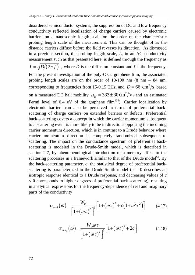
Chapter 4 – Study 1: Broadband terahertz time-domain conductance spectroscopy and imaging…
72
disordered semiconductor systems, the suppression of DC and low frequency
conductivity reflected localization of charge carriers caused by electronic
barriers on a nanoscopic length scale on the order of the characteristic
probing length scale of the measurement. This can be thought of as the
distance carriers diffuse before the field reverses its direction. As discussed
in a previous section, the probing length scale, L, in an AC conductivity
measurement such as that presented here, is defined through the frequency as
2L D f , where D is the diffusion constant and f is the frequency.
For the present investigation of the poly-C Cu graphene film, the associated
probing length scales are on the order of 10-100 nm (8 nm – 84 nm,
corresponding to frequencies from 15-0.15 THz, and 266 cm sD based
on a measured DC hall mobility 2333 30cm VsH and an estimated
Fermi level of 0.4 eV of the graphene film136
). Carrier localization by
electronic barriers can also be perceived in terms of preferential back-
scattering of charge carriers on extended barriers or defects. Preferential
back-scattering covers a concept in which the carrier momentum subsequent
to a scattering event is more likely to be in directions opposing the incoming
carrier momentum direction, which is in contrast to a Drude behavior where
carrier momentum direction is completely randomized subsequent to
scattering. The impact on the conductance spectrum of preferential back-
scattering is modeled in the Drude-Smith model, which is described in
section 2.7, by phenomenological introduction of a memory effect to the
scattering processes in a framework similar to that of the Drude model65
. By
the back-scattering parameter, c, the statistical degree of preferential back-
scattering is parameterized in the Drude-Smith model (c = 0 describes an
isotropic response identical to a Drude response, and decreasing values of c
< 0 corresponds to higher degrees of preferential back-scattering), resulting
in analytical expressions for the frequency-dependence of real and imaginary
parts of the conductivity
2 2 2
22
1 1
1
Dreal
Wc
(4.17)
2
22
1 2
1
Dimag
Wc
(4.18)
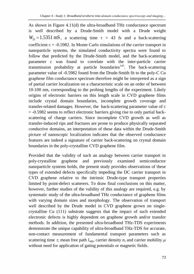
Chapter 4 - Study 1: Broadband terahertz time-domain conductance spectroscopy and imaging…
73
As shown in Figure 4.11(d) the ultra-broadband THz conductance spectrum
is well described by a Drude-Smith model with a Drude weight
1.5351 mSDW , a scattering time = 43 fs and a back-scattering
coefficient c = -0.5982. In Monte Carlo simulations of the carrier transport in
nanoparticle systems, the simulated conductivity spectra were found to
follow that predicted by the Drude-Smith model, and the back-scattering
parameter c was found to correlate with the inter-particle carrier
transmission probability at particle boundaries143
. The back-scattering
parameter value of -0.5982 found from the Drude-Smith fit to the poly-C Cu
graphene film conductance spectrum therefore might be interpreted as a sign
of partial carrier localization on a characteristic scale on an order of between
10-100 nm, corresponding to the probing lengths of the experiment. Likely
origins of electronic barriers on this length scale in CVD graphene films
include crystal domain boundaries, incomplete growth coverage and
transfer-related damages. However, the back-scattering parameter value of c
= -0.5982 seems to reflect electronic barriers giving rise to only partial back-
scattering of charge carriers. Since incomplete CVD growth as well as
transfer-induced rips and fractures are prone to produce physically separated
conductive domains, an interpretation of these data within the Drude-Smith
picture of nanoscopic localization indicates that the observed conductance
features are indeed a signature of carrier back-scattering on crystal domain
boundaries in the poly-crystalline CVD graphene film.
Provided that the validity of such an analogy between carrier transport in
poly-crystalline graphene and previously examined semiconductor
nanoparticle systems holds, the present study provides observations of these
types of extended defects specifically impeding the DC carrier transport in
CVD graphene relative to the intrinsic Drude-type transport properties
limited by point-defect scatterers. To draw final conclusions on this matter,
however, further studies of the validity of this analogy are required, e.g. by
systematic study of the ultra-broadband THz conductance of graphene films
with varying domain sizes and morphology. The observation of transport
well described by the Drude model in CVD graphene grown on single-
crystalline Cu (111) substrate suggests that the impact of such extended
electronic defects is highly dependent on graphene growth and/or transfer
methods. In addition, the presented ultra-broadband THz-TDS experiments
demonstrate the unique capability of ultra-broadband THz-TDS for accurate,
non-contact measurement of fundamental transport parameters such as
scattering time , mean free path lmfp, carrier density ns and carrier mobility
without need for application of gating potentials or magnetic fields.
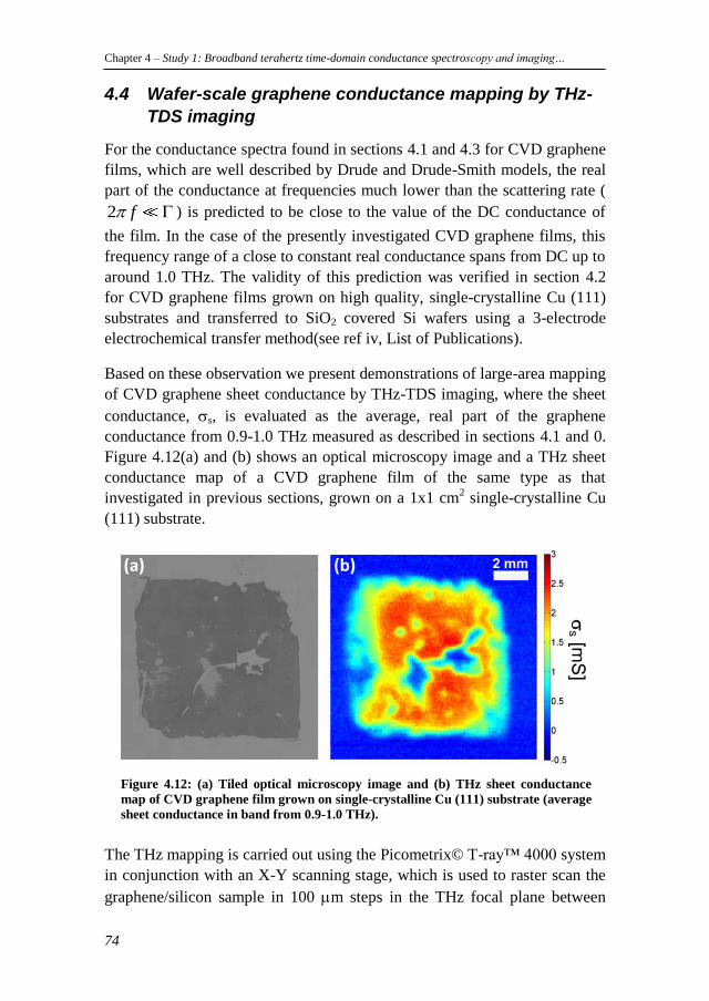
Chapter 4 – Study 1: Broadband terahertz time-domain conductance spectroscopy and imaging…
74
4.4 Wafer-scale graphene conductance mapping by THz-
TDS imaging
For the conductance spectra found in sections 4.1 and 4.3 for CVD graphene
films, which are well described by Drude and Drude-Smith models, the real
part of the conductance at frequencies much lower than the scattering rate (
2 f ) is predicted to be close to the value of the DC conductance of
the film. In the case of the presently investigated CVD graphene films, this
frequency range of a close to constant real conductance spans from DC up to
around 1.0 THz. The validity of this prediction was verified in section 4.2
for CVD graphene films grown on high quality, single-crystalline Cu (111)
substrates and transferred to SiO2 covered Si wafers using a 3-electrode
electrochemical transfer method(see ref iv, List of Publications).
Based on these observation we present demonstrations of large-area mapping
of CVD graphene sheet conductance by THz-TDS imaging, where the sheet
conductance, s, is evaluated as the average, real part of the graphene
conductance from 0.9-1.0 THz measured as described in sections 4.1 and 0.
Figure 4.12(a) and (b) shows an optical microscopy image and a THz sheet
conductance map of a CVD graphene film of the same type as that
investigated in previous sections, grown on a 1x1 cm2 single-crystalline Cu
(111) substrate.
Figure 4.12: (a) Tiled optical microscopy image and (b) THz sheet conductance
map of CVD graphene film grown on single-crystalline Cu (111) substrate (average
sheet conductance in band from 0.9-1.0 THz).
The THz mapping is carried out using the Picometrix© T-ray™ 4000 system
in conjunction with an X-Y scanning stage, which is used to raster scan the
graphene/silicon sample in 100 m steps in the THz focal plane between
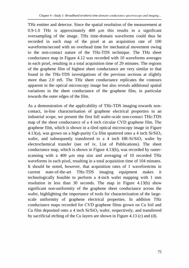
Chapter 4 - Study 1: Broadband terahertz time-domain conductance spectroscopy and imaging…
75
THz emitter and detector. Since the spatial resolution of the measurement at
0.9-1.0 THz is approximately 400 m this results in a significant
oversampling of the image. THz time-domain waveforms could thus be
recorded in each map of the pixel at an acquisition rate of 100
waveforms/second with no overhead time for mechanical movement owing
to the non-contact nature of the THz-TDS technique. The THz sheet
conductance map in Figure 4.12 was recorded with 10 waveforms averages
in each pixel, resulting in a total acquisition time of 29 minutes. The regions
of the graphene film of highest sheet conductance are very similar to that
found in the THz-TDS investigations of the previous sections at slightly
more than 2.0 mS. The THz sheet conductance replicates the contours
apparent in the optical microscopy image but also reveals additional spatial
variations in the sheet conductance of the graphene film, in particular
towards the outer edges of the film.
As a demonstration of the applicability of THz-TDS imaging towards non-
contact, in-line characterisation of graphene electrical properties in an
industrial scope, we present the first full wafer-scale non-contact THz-TDS
map of the sheet conductance of a 4 inch circular CVD graphene film. The
graphene film, which is shown in a tiled optical microscopy image in Figure
4.13(a), was grown on a high-purity Cu film sputtered onto a 4 inch Si/SiO2
wafer, and subsequently transferred to a 4 inch HR-Si/SiO2 wafer by
electrochemical transfer (see ref iv, List of Publications). The sheet
conductance map, which is shown in Figure 4.13(b), was recorded by raster-
scanning with a 400 m step size and averaging of 10 recorded THz
waveforms in each pixel, resulting in a total acquisition time of 104 minutes.
It should be noted, however, that acquisition rates of 1 waveform/ms in
current state-of-the-art THz-TDS imaging equipment makes it
technologically feasible to perform a 4-inch wafer mapping with 1 mm
resolution in less than 30 seconds. The map in Figure 4.13(b) show
significant non-uniformity of the graphene sheet conductance across the
wafer, highlighting the importance of tools for characterization of the large-
scale uniformity of graphene electrical properties. In addition THz
conductance maps recorded for CVD graphene films grown on Cu foil and
Cu film deposited onto a 4 inch Si/SiO2 wafer, respectively, and transferred
by sacrificial etching of the Cu layers are shown in Figure 4.13 (c) and (d).
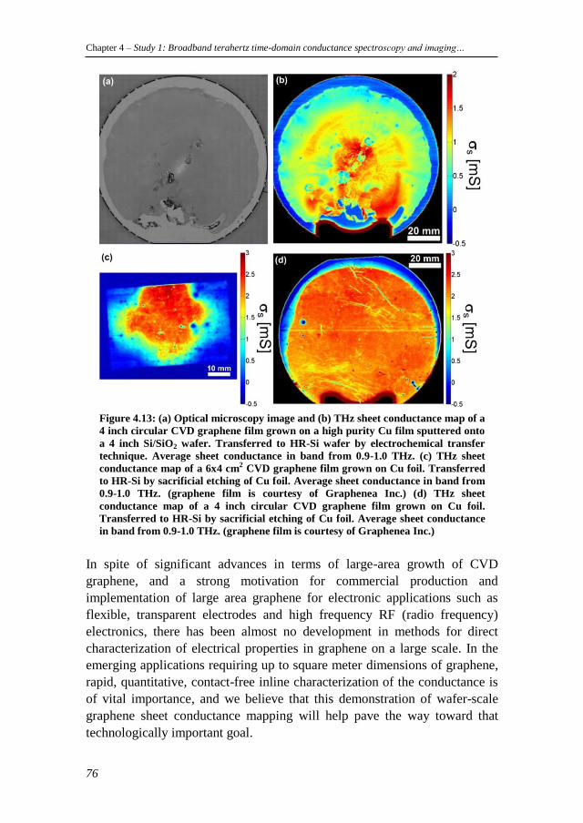
Chapter 4 – Study 1: Broadband terahertz time-domain conductance spectroscopy and imaging…
76
Figure 4.13: (a) Optical microscopy image and (b) THz sheet conductance map of a
4 inch circular CVD graphene film grown on a high purity Cu film sputtered onto
a 4 inch Si/SiO2 wafer. Transferred to HR-Si wafer by electrochemical transfer
technique. Average sheet conductance in band from 0.9-1.0 THz. (c) THz sheet
conductance map of a 6x4 cm2 CVD graphene film grown on Cu foil. Transferred
to HR-Si by sacrificial etching of Cu foil. Average sheet conductance in band from
0.9-1.0 THz. (graphene film is courtesy of Graphenea Inc.) (d) THz sheet
conductance map of a 4 inch circular CVD graphene film grown on Cu foil.
Transferred to HR-Si by sacrificial etching of Cu foil. Average sheet conductance
in band from 0.9-1.0 THz. (graphene film is courtesy of Graphenea Inc.)
In spite of significant advances in terms of large-area growth of CVD
graphene, and a strong motivation for commercial production and
implementation of large area graphene for electronic applications such as
flexible, transparent electrodes and high frequency RF (radio frequency)
electronics, there has been almost no development in methods for direct
characterization of electrical properties in graphene on a large scale. In the
emerging applications requiring up to square meter dimensions of graphene,
rapid, quantitative, contact-free inline characterization of the conductance is
of vital importance, and we believe that this demonstration of wafer-scale
graphene sheet conductance mapping will help pave the way toward that
technologically important goal.
Chapter 4 - Study 1: Broadband terahertz time-domain conductance spectroscopy and imaging…
77
Chapter 4 – Study 1: Broadband terahertz time-domain conductance spectroscopy and imaging…
78
79
5 Study 2: THz and M4PP large area
conductance mapping and correlation – a
new light on defects
5.1 Corrections
It should be noted that new insight into the carrier dynamics of one of the
graphene films presented in this chapter have been obtained after the time of
the presented investigation. A more complete view of the carrier dynamics
was facilitated by the ultra-broadband THz-TDS measurements presented in
section 3.2. These indicate that in spite of early observations of a frequency-
independent conductance response from 0.15-1.5 THz, the conductance of
the graphene film is to some extent affected by extended electrical defects on
a nanoscopic scale. Some of the conclusions relating to the nanoscopic
electrical continuity of the investigated graphene films may therefore be
subject to modifications. The investigation in section 4.3, suggests that the
DC conductance of the investigated films may be suppressed due to
extended electrical defects on the nanoscopic scale. The key conclusion of
this chapter, stating that the microscopic DC conductance is reduced relative
to the nanoscopic counterpart due to electrical defects on a scale on the order
of 10 m, however, remains unaffected.
Chapter 5 – Study 2: THz and M4PP large are conductance mapping and correlation – a new light…
80
5.2 Introduction
After the seminal work on graphene1,3
, its potential use in commercially
lucrative technologies has initiated impressive progress in research into
graphene-based technologies. Examples of electronic applications include
integrated circuits144
, THz bandwidth RF electronics145
and spintronics146
,
and photonic and optoelectronic applications include photovoltaic55
and
light-emitting devices147
, saturable absorbers148
, optical limiters149
, nonlinear
frequency conversion150
, and THz devices151
. In particular, extended areas of
single- or few-layer graphene will have a strong, positive impact as
transparent conductors in photovoltaic devices and touch-screen devices,
with the potential of replacing expensive and scarce materials152
such as
indium tin oxide. The potential use of graphene in this range of important
technologies has sparked impressive progress in the number of available
techniques for the large-scale synthesis of high-quality graphene in terms of
electrical, mechanical and optical properties over large areas54,57,136,153,154
.
However, development of techniques targeting electrical characterization of
graphene on a large scale has not kept pace, leaving the rapidly progressing
field with inadequate means of assessing the electrical uniformity of
synthesized films.
The electrical characterization of large area graphene that takes place today
comprises ‘off-line’ transport measurements in lithographically defined
structures such as Hall bar devices or time-consuming scanning tunneling
microscopy and conductance atomic force microscopy measurements. None
of these methods are suitable for high throughput characterization or for
investigation of the large-scale uniformity and quality of graphene films with
respect to electronic properties.
In recent years it has been shown that THz spectroscopy155
, used extensively
to measure frequency-resolved conductance of bulk semiconductors156
and
semiconductor nanostructures68
, is a powerful method for investigating the
electronic response of graphene, either in the embodiment of THz Fourier-
Transform Infrared Spectroscopy44
or THz time-domain spectroscopy (THz-
TDS)122–124,127,128
, the latter also enabling ultrafast pump-probe investigations
of THz conductance. It was also recently shown that the electronic response
of single atomic layer of chemical vapor deposited (CVD) graphene can be
imaged using THz-TDS121,157
. Because of the non-contact nature of the THz-
TDS technique, mapping of unimpaired electronic properties, which can
otherwise be affected by formation of ohmic graphene-metal contact
interfaces158–161
, can be carried out without risk of damage, and with a
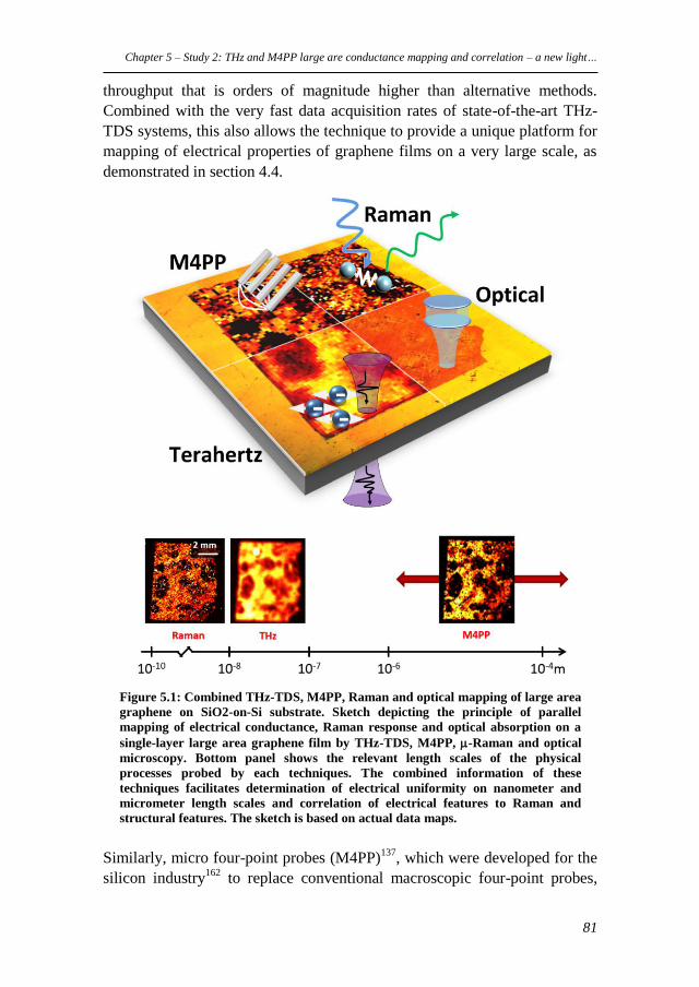
Chapter 5 – Study 2: THz and M4PP large are conductance mapping and correlation – a new light…
81
throughput that is orders of magnitude higher than alternative methods.
Combined with the very fast data acquisition rates of state-of-the-art THz-
TDS systems, this also allows the technique to provide a unique platform for
mapping of electrical properties of graphene films on a very large scale, as
demonstrated in section 4.4.
Figure 5.1: Combined THz-TDS, M4PP, Raman and optical mapping of large area
graphene on SiO2-on-Si substrate. Sketch depicting the principle of parallel
mapping of electrical conductance, Raman response and optical absorption on a
single-layer large area graphene film by THz-TDS, M4PP, -Raman and optical
microscopy. Bottom panel shows the relevant length scales of the physical
processes probed by each techniques. The combined information of these
techniques facilitates determination of electrical uniformity on nanometer and
micrometer length scales and correlation of electrical features to Raman and
structural features. The sketch is based on actual data maps.
Similarly, micro four-point probes (M4PP)137
, which were developed for the
silicon industry162
to replace conventional macroscopic four-point probes,
Chapter 5 – Study 2: THz and M4PP large are conductance mapping and correlation – a new light…
82
van der Pauw technique, and spreading resistance probes because these
methods lack reliability163–168
and spatial resolution162,169
when applied to
advanced semiconductor layered structures, have recently been demonstrated
as a tool for non-destructive characterization of graphene sheet
conductance170
. In sections 4.2.2 and 4.2.3, the M4PP technique was also
applied for measurement of the microscopic/macroscopic DC conductance
of CVD graphene films. For a description of the technique, the reader is
referred to section 4.2.1.
In this chapter, a demonstration of correlated M4PP and non-contact THz-
TDS measurements for centimeter scale quantitative mapping of the sheet
conductance of large-area CVD graphene films is presented. It is shown that
dual configuration M4PP measurements provide valuable statistical insight
into the influence on the conductance of micro-scale defects, while THz-
TDS imaging can probe the influence of nano-scale defects. THz-TDS
furthermore has potential as a fast, non-contact metrology method for
mapping of the spatially averaged nanoscopic conductance on wafer-scale
graphene, with scan times of less than a minute for a 4 inch wafer.
The combination of M4PP and THz-TDS conductance measurements,
supported by micro Raman spectroscopy and optical imaging reveals that the
film is electrically continuous on the nanoscopic scale, but dominated in its
micro-scale conductance by microscopic defects, likely originating from the
transfer process. The conductance maps measured by M4PP and THz-TDS
agree qualitatively with each other, showing a correlation indicative of the
sensitivity of the two techniques towards electrical defects on different
length scales, in agreement with the observations made in section 4.2.3. The
M4PP measurements probe the microscopic sheet conductance and are
particularly sensitive to micro-scale electrical defects in the graphene sheet,
while THz-TDS measurements probe the spatially averaged nanoscopic
sheet conductance, due to the very high frequency alternating current (AC)
electric fields of the THz radiation. Through correlation of M4PP and THz-
TDS maps, it is found that microscopic defects, likely originating from the
transfer process dominate the micro-scale conductance of the investigated
graphene film. Correlations with micro Raman spectroscopy (-Raman)
maps and optical images of the CVD graphene film support this notion.
Chapter 5 – Study 2: THz and M4PP large are conductance mapping and correlation – a new light…
83
5.3 Experimental details
Mapping of the electrical conductance uniformity is carried out by M4PP
and non-contact THz-TDS as well as mapping of the Raman response of
centimeter scale CVD graphene transferred onto high resistivity silicon (
5,000 Ω cm ) substrates covered with 90 nm SiO2, cf. Figure 5.1(a).
Two graphene samples grown by different recipes and transfer processes
were investigated.
The first sample (labeled “sample 1” in the following) is the apparently least
damaged graphene film, with dimensions of 2x2 cm2. It was grown in a
vertical furnace, where a 25 m thick copper foil was first annealed in
hydrogen at a temperature of 1025o
C and pressure of 0.133 mbar. The
growth time was approximately 25 minutes during which the system was
maintained at a pressure of 2 mbar and temperature of 1025 oC, with a
methane flow of 2 standard cubic centimeters per minute (sccm) and a
hydrogen flow of 0.5 sccm. These parameters are similar to previously
reported conditions for monolayer graphene growth24,54
. The grown graphene
film was then transferred to a high resistivity silicon wafer by slow etching
the copper foil in a solution of 0.1M ammonium persulfate ((NH4)2S2O8)
with a thin supporting polymethylmethacrylate (PMMA) layer. The PMMA
was subsequently removed in acetone.
The second sample (labeled “sample 2”) is a 6 7 mm graphene film with
distinct optically visible damages. It was grown in a cold-wall CVD system
using pre-diluted CH4 (5% in Ar) as carbon precursor. The deposition
temperature was nominally 1000o
C and the growth time was 5 min. H2 and
Ar were used as auxiliary gases, where the partial pressure of CH4 was kept
very low (<0.01 mbar) to suppress the formation of multilayer flakes and
enhance the quality and domain size of the graphene. More details about this
CVD procedure are reported elsewhere171–173
. The as-deposited graphene was
subsequently transferred onto high resistivity silicon by a standard wet
transfer process using PMMA as mechanical support and a dilute, aqueous
HNO3 solution to etch the copper film54,171
. Finally, the polymer was
removed by acetone.
The Raman response of the samples was mapped using a Thermo Fisher
Scientific DXR -Raman microscope with a 532 nm excitation laser and a 2
m spotsize. Spatial maps of the samples were produced with 200 µm and
75 µm lateral resolution for sample 1 and sample 2, respectively, providing
spectroscopic information between 1100 and 3000 cm-1
(1 cm-1
resolution) in
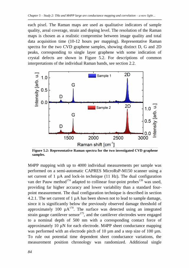
Chapter 5 – Study 2: THz and M4PP large are conductance mapping and correlation – a new light…
84
each pixel. The Raman maps are used as qualitative indicators of sample
quality, areal coverage, strain and doping level. The resolution of the Raman
maps is chosen as a realistic compromise between image quality and total
data acquisition time (10-12 hours per mapping). Representative Raman
spectra for the two CVD graphene samples, showing distinct D, G and 2D
peaks, corresponding to single layer graphene with some indication of
crystal defects are shown in Figure 5.2. For descriptions of common
interpretations of the individual Raman bands, see section 2.2.
Figure 5.2: Representative Raman spectra for the two investigated CVD graphene
samples.
M4PP mapping with up to 4000 individual measurements per sample was
performed on a semi-automatic CAPRES MicroRsP-M150 scanner using a
set current of 1 µA and lock-in technique (11 Hz). The dual configuration
van der Pauw method174
adapted to collinear four-point probes139
was used,
providing far higher accuracy and lower variability than a standard four-
point measurement. The dual configuration technique is described in section
4.2.1. The set current of 1 µA has been shown not to lead to sample damage,
since it is significantly below the previously observed damage threshold of
approximately 100 µA170
. The surface was detected using an integrated
strain gauge cantilever sensor175
, and the cantilever electrodes were engaged
to a nominal depth of 500 nm with a corresponding contact force of
approximately 10 µN for each electrode. M4PP sheet conductance mapping
was performed with an electrode pitch of 10 µm and a step size of 100 µm.
To rule out potential time dependent sheet conductance variations, the
measurement position chronology was randomized. Additional single
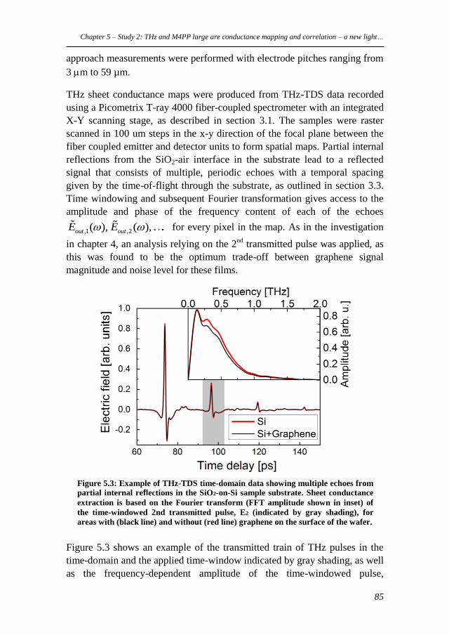
Chapter 5 – Study 2: THz and M4PP large are conductance mapping and correlation – a new light…
85
approach measurements were performed with electrode pitches ranging from
3 m to 59 µm.
THz sheet conductance maps were produced from THz-TDS data recorded
using a Picometrix T-ray 4000 fiber-coupled spectrometer with an integrated
X-Y scanning stage, as described in section 3.1. The samples were raster
scanned in 100 um steps in the x-y direction of the focal plane between the
fiber coupled emitter and detector units to form spatial maps. Partial internal
reflections from the SiO2-air interface in the substrate lead to a reflected
signal that consists of multiple, periodic echoes with a temporal spacing
given by the time-of-flight through the substrate, as outlined in section 3.3.
Time windowing and subsequent Fourier transformation gives access to the
amplitude and phase of the frequency content of each of the echoes
,1 ,2( ), ( ),out outE E for every pixel in the map. As in the investigation
in chapter 4, an analysis relying on the 2nd
transmitted pulse was applied, as
this was found to be the optimum trade-off between graphene signal
magnitude and noise level for these films.
Figure 5.3: Example of THz-TDS time-domain data showing multiple echoes from
partial internal reflections in the SiO2-on-Si sample substrate. Sheet conductance
extraction is based on the Fourier transform (FFT amplitude shown in inset) of
the time-windowed 2nd transmitted pulse, E2 (indicated by gray shading), for
areas with (black line) and without (red line) graphene on the surface of the wafer.
Figure 5.3 shows an example of the transmitted train of THz pulses in the
time-domain and the applied time-window indicated by gray shading, as well
as the frequency-dependent amplitude of the time-windowed pulse,
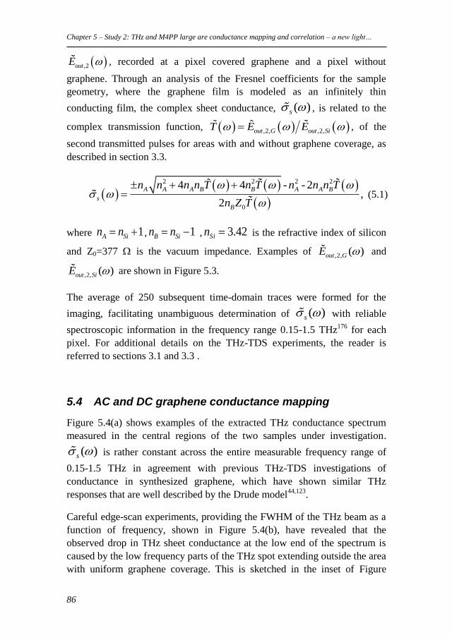
Chapter 5 – Study 2: THz and M4PP large are conductance mapping and correlation – a new light…
86
,2outE , recorded at a pixel covered graphene and a pixel without
graphene. Through an analysis of the Fresnel coefficients for the sample
geometry, where the graphene film is modeled as an infinitely thin
conducting film, the complex sheet conductance, ( )s , is related to the
complex transmission function, ,2, ,2,out G out SiT E E , of the
second transmitted pulses for areas with and without graphene coverage, as
described in section 3.3.
2 2 2 2
0
4 4 - - 2,
2
A A A B B A A B
s
B
n n n n T n T n n n T
n Z T
(5.1)
where 1A Sin n , 1B Sin n , 42.3Sin is the refractive index of silicon
and Z0=377 is the vacuum impedance. Examples of ,2, ( )out GE
and
,2, ( )out SiE are shown in Figure 5.3.
The average of 250 subsequent time-domain traces were formed for the
imaging, facilitating unambiguous determination of ( )s with reliable
spectroscopic information in the frequency range 0.15-1.5 THz176
for each
pixel. For additional details on the THz-TDS experiments, the reader is
referred to sections 3.1 and 3.3 .
5.4 AC and DC graphene conductance mapping
Figure 5.4(a) shows examples of the extracted THz conductance spectrum
measured in the central regions of the two samples under investigation.
( )s is rather constant across the entire measurable frequency range of
0.15-1.5 THz in agreement with previous THz-TDS investigations of
conductance in synthesized graphene, which have shown similar THz
responses that are well described by the Drude model44,123
.
Careful edge-scan experiments, providing the FWHM of the THz beam as a
function of frequency, shown in Figure 5.4(b), have revealed that the
observed drop in THz sheet conductance at the low end of the spectrum is
caused by the low frequency parts of the THz spot extending outside the area
with uniform graphene coverage. This is sketched in the inset of Figure
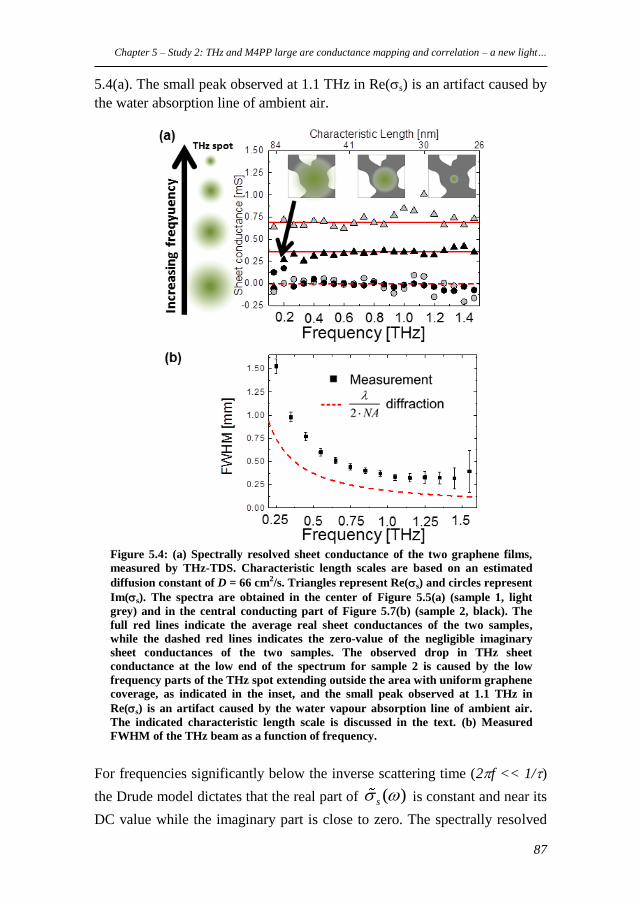
Chapter 5 – Study 2: THz and M4PP large are conductance mapping and correlation – a new light…
87
5.4(a). The small peak observed at 1.1 THz in Re(s) is an artifact caused by
the water absorption line of ambient air.
Figure 5.4: (a) Spectrally resolved sheet conductance of the two graphene films,
measured by THz-TDS. Characteristic length scales are based on an estimated
diffusion constant of D = 66 cm2/s. Triangles represent Re(s) and circles represent
Im(s). The spectra are obtained in the center of Figure 5.5(a) (sample 1, light
grey) and in the central conducting part of Figure 5.7(b) (sample 2, black). The
full red lines indicate the average real sheet conductances of the two samples,
while the dashed red lines indicates the zero-value of the negligible imaginary
sheet conductances of the two samples. The observed drop in THz sheet
conductance at the low end of the spectrum for sample 2 is caused by the low
frequency parts of the THz spot extending outside the area with uniform graphene
coverage, as indicated in the inset, and the small peak observed at 1.1 THz in
Re(s) is an artifact caused by the water vapour absorption line of ambient air.
The indicated characteristic length scale is discussed in the text. (b) Measured
FWHM of the THz beam as a function of frequency.
For frequencies significantly below the inverse scattering time (2f << 1/)
the Drude model dictates that the real part of ( )s is constant and near its
DC value while the imaginary part is close to zero. The spectrally resolved
Chapter 5 – Study 2: THz and M4PP large are conductance mapping and correlation – a new light…
88
THz-TDS conductance measurement can thus be replaced by a single, real-
valued quantity which can be compared directly to DC sheet conductance
value as determined by M4PP measurements. In the sheet conductance
mappings the THz-frequency conductance is represented by its average
value in the region 1.3-1.4 THz as this range offers the optimum trade-off
between the obtainable spatial resolution and signal-to-noise ratio of the
measurements. With increased bandwidth, the THz-TDS technique also
allows determination of the Drude carrier scattering time through fitting of
the characteristic Drude model to the spectrum, as shown in chapter 0.
Figure 5.4(b) shows the full-width-at-half-maximum (FWHM) of the THz
beam as a function of frequency, inferred from the average rise distance of
the THz amplitude response on the left edge of the graphene film in Figure
5.5. These measurements show that the THz spot diameter is approximately
0.32 mm FWHM in the 1.3-1.4 THz frequency range. This results in some
blurring, as variations on a smaller length scale are not accurately
reproduced.
Figure 5.5: Images of homogeneous CVD grown graphene film on 90 nm SiO2 on
Si (sample 1). Scale bars are 2 mm. (a) THz sheet conductance map. Average sheet
conductance in 1.3-1.4 THz band. (b) Tiled optical microscope image.
Figure 5.5(a) shows direct mapping of the magnitude and uniformity of s,THz
at 1.3-1.4 THz recorded by THz-TDS across the CVD graphene film with
dimensions of approximately 2 x 2 cm2 (sample 1), revealing an electrically
homogeneous film. The Raman maps of the graphene film are fairly
homogeneous, as shown in Figure 5.6, with the exception of one region of
spectral redshift of the Raman D, G and 2D peaks, as shown in Figure
5.6(d), (e) and (f). This type of redshift is commonly interpreted as an
indicator of local strain in the graphene film24
. This strain does not seem to
have a significant influence on s,THz of this particular graphene film,
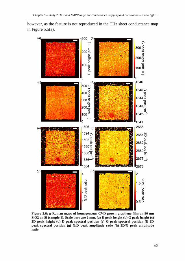
Chapter 5 – Study 2: THz and M4PP large are conductance mapping and correlation – a new light…
89
however, as the feature is not reproduced in the THz sheet conductance map
in Figure 5.5(a).
Figure 5.6: -Raman maps of homogeneous CVD grown graphene film on 90 nm
SiO2 on Si (sample 1). Scale bars are 2 mm. (a) D peak height (b) G peak height (c)
2D peak height (d) D peak spectral position (e) G peak spectral position (f) 2D
peak spectral position (g) G/D peak amplitude ratio (h) 2D/G peak amplitude
ratio.
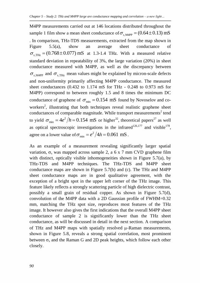
Chapter 5 – Study 2: THz and M4PP large are conductance mapping and correlation – a new light…
90
M4PP measurements carried out at 146 locations distributed throughout the
sample 1 film show a mean sheet conductance of ,M4PP (0.64 0.13) mSs
. In comparison, THz-TDS measurements, extracted from the map shown in
Figure 5.5(a), show an average sheet conductance of
,THz (0.768 0.077) mSs at 1.3-1.4 THz. With a measured relative
standard deviation in repeatability of 3%, the large variation (20%) in sheet
conductance measured with M4PP, as well as the discrepancy between
,M4PPs and ,THzs mean values might be explained by micron-scale defects
and non-uniformity primarily affecting M4PP conductance. The measured
sheet conductances (0.432 to 1.174 mS for THz - 0.248 to 0.973 mS for
M4PP) correspond to between roughly 1.5 and 8 times the minimum DC
conductance of graphene of min 0.154 mS found by Novoselov and co-
workers2, illustrating that both techniques reveal realistic graphene sheet
conductances of comparable magnitude. While transport measurements2 tend
to yield 2
min 4 0.154 mSe h or higher32
, theoretical papers27
as well
as optical spectroscopic investigations in the infrared126,177
and visible178
,
agree on a lower value of2
min 4 0.061 mSe .
As an example of a measurement revealing significantly larger spatial
variation, s was mapped across sample 2, a 6 x 7 mm CVD graphene film
with distinct, optically visible inhomogeneities shown in Figure 5.7(a), by
THz-TDS and M4PP techniques. The THz-TDS and M4PP sheet
conductance maps are shown in Figure 5.7(b) and (c). The THz and M4PP
sheet conductance maps are in good qualitative agreement, with the
exception of a bright spot in the upper left corner of the THz image. This
feature likely reflects a strongly scattering particle of high dielectric contrast,
possibly a small grain of residual copper. As shown in Figure 5.7(d),
convolution of the M4PP data with a 2D Gaussian profile of FWHM=0.32
mm, matching the THz spot size, reproduces most features of the THz
image. It however also gives the first indications that the overall M4PP sheet
conductance of sample 2 is significantly lower than the THz sheet
conductance, as will be discussed in detail in the next section. A comparison
of THz and M4PP maps with spatially resolved -Raman measurements,
shown in Figure 5.8, reveals a strong spatial correlation, most prominent
between s and the Raman G and 2D peak heights, which follow each other
closely.
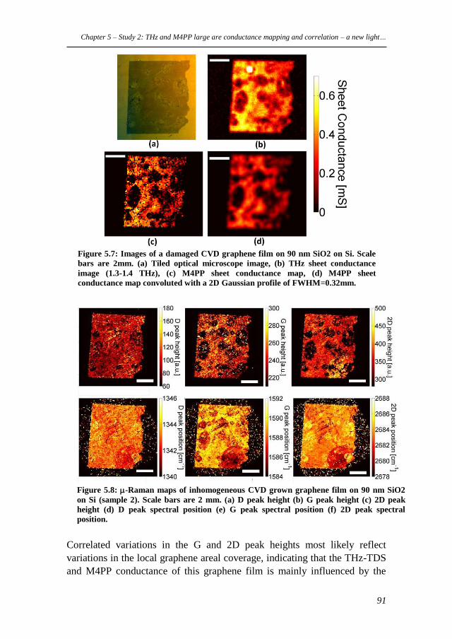
Chapter 5 – Study 2: THz and M4PP large are conductance mapping and correlation – a new light…
91
Figure 5.7: Images of a damaged CVD graphene film on 90 nm SiO2 on Si. Scale
bars are 2mm. (a) Tiled optical microscope image, (b) THz sheet conductance
image (1.3-1.4 THz), (c) M4PP sheet conductance map, (d) M4PP sheet
conductance map convoluted with a 2D Gaussian profile of FWHM=0.32mm.
Figure 5.8: -Raman maps of inhomogeneous CVD grown graphene film on 90 nm SiO2
on Si (sample 2). Scale bars are 2 mm. (a) D peak height (b) G peak height (c) 2D peak
height (d) D peak spectral position (e) G peak spectral position (f) 2D peak spectral
position.
Correlated variations in the G and 2D peak heights most likely reflect
variations in the local graphene areal coverage, indicating that the THz-TDS
and M4PP conductance of this graphene film is mainly influenced by the
Chapter 5 – Study 2: THz and M4PP large are conductance mapping and correlation – a new light…
92
local density of rips and defects induced by the transfer or by incomplete
growth coverage. Other parameters identifiable by -Raman analysis, such
as atomic defects, doping level and strain seem to be of secondary
importance. There are also spatial features in the measured sheet
conductance that are not reflected in the -Raman data, showing that direct
sheet conductance mapping of CVD graphene films provide valuable
additional information about sheet conductance uniformity that cannot be
inferred from Raman analysis.
5.5 New light on electrical defects: Correlating THz and
DC conductivity
A quantitative correlation analysis between THz and M4PP images of
sample 2 (Figure 5.7(b) and (c)) is shown in Figure 5.9(a) and (b), where the
corresponding values for s,M4PP and s,THz have been plotted against each
other for all pixels where the M4PP measurement yielded a finite and non-
zero conductance.
The subset of points with= s,M4PP/s,THz > 1.1, shown with red dots in
Figure 5.9(a) and (b), is related to a lowering of the measured s,THz near
edges of the film due to spot size blurring. If the measurements caused by
this edge effect are ignored, it is evident that there is a tendency for the
M4PP sheet conductance to be lower than that measured by THz-TDS.
Although based on a smaller measurement population, the same tendency is
observed in the correlation plot of THz and M4PP measurement from sample
1, shown in Figure 5.9(a). As will be discussed below, this behavior stems
from the different ways in which THz and M4PP measurements are affected
by micron-scale defects such as rips, wrinkles (transfer defects) and domain
boundaries (growth defects) in the graphene film.
The M4PP conductance measurement probes carrier transport on the scale of
the 10 m electrode pitch, and is therefore very sensitive to microscopic
defects. Rip-like defects or domain boundaries smaller than the electrode
pitch of 10 m may substantially decrease the measureds,M4PP, even by
orders of magnitude, compared to the case of a defect-free sheet179,180
. Also
insulating rips or boundaries of dimensions similar to the electrode pitch can
in the worst case result in an underestimation of the sheet conductance by up
to a factor of two140
. The presence of a high density of defects of dimensions
similar to the electrode pitch is indeed indicated in the graphene sample
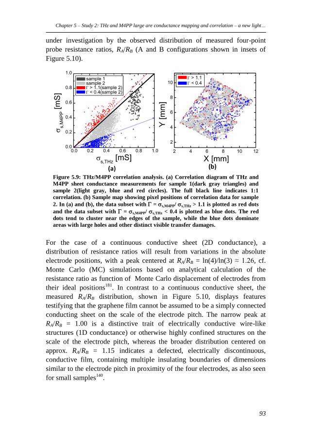
Chapter 5 – Study 2: THz and M4PP large are conductance mapping and correlation – a new light…
93
under investigation by the observed distribution of measured four-point
probe resistance ratios, RA/RB (A and B configurations shown in insets of
Figure 5.10).
Figure 5.9: THz/M4PP correlation analysis. (a) Correlation diagram of THz and
M4PP sheet conductance measurements for sample 1(dark gray triangles) and
sample 2(light gray, blue and red circles). The full black line indicates 1:1
correlation. (b) Sample map showing pixel positions of correlation data for sample
2. In (a) and (b), the data subset with = s,M4PP/ s,THz > 1.1 is plotted as red dots
and the data subset with = s,M4PP/ s,THz < 0.4 is plotted as blue dots. The red
dots tend to cluster near the edges of the sample, while the blue dots dominate
areas with large holes and other distinct visible transfer damages.
For the case of a continuous conductive sheet (2D conductance), a
distribution of resistance ratios will result from variations in the absolute
electrode positions, with a peak centered at RA/RB = ln(4)/ln(3) ≈ 1.26, cf.
Monte Carlo (MC) simulations based on analytical calculation of the
resistance ratio as function of Monte Carlo displacement of electrodes from
their ideal positions181
. In contrast to a continuous conductive sheet, the
measured RA/RB distribution, shown in Figure 5.10, displays features
testifying that the graphene film cannot be assumed to be a simply connected
conducting sheet on the scale of the electrode pitch. The narrow peak at
RA/RB = 1.00 is a distinctive trait of electrically conductive wire-like
structures (1D conductance) or otherwise highly confined structures on the
scale of the electrode pitch, whereas the broader distribution centered on
approx. RA/RB = 1.15 indicates a defected, electrically discontinuous,
conductive film, containing multiple insulating boundaries of dimensions
similar to the electrode pitch in proximity of the four electrodes, as also seen
for small samples140
.
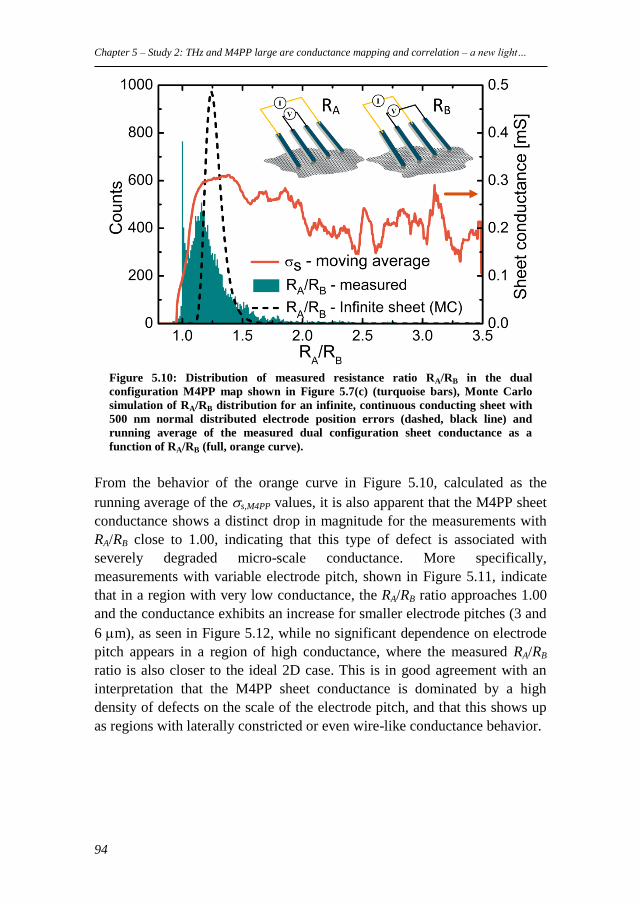
Chapter 5 – Study 2: THz and M4PP large are conductance mapping and correlation – a new light…
94
Figure 5.10: Distribution of measured resistance ratio RA/RB in the dual
configuration M4PP map shown in Figure 5.7(c) (turquoise bars), Monte Carlo
simulation of RA/RB distribution for an infinite, continuous conducting sheet with
500 nm normal distributed electrode position errors (dashed, black line) and
running average of the measured dual configuration sheet conductance as a
function of RA/RB (full, orange curve).
From the behavior of the orange curve in Figure 5.10, calculated as the
running average of the s,M4PP values, it is also apparent that the M4PP sheet
conductance shows a distinct drop in magnitude for the measurements with
RA/RB close to 1.00, indicating that this type of defect is associated with
severely degraded micro-scale conductance. More specifically,
measurements with variable electrode pitch, shown in Figure 5.11, indicate
that in a region with very low conductance, the RA/RB ratio approaches 1.00
and the conductance exhibits an increase for smaller electrode pitches (3 and
6 m), as seen in Figure 5.12, while no significant dependence on electrode
pitch appears in a region of high conductance, where the measured RA/RB
ratio is also closer to the ideal 2D case. This is in good agreement with an
interpretation that the M4PP sheet conductance is dominated by a high
density of defects on the scale of the electrode pitch, and that this shows up
as regions with laterally constricted or even wire-like conductance behavior.
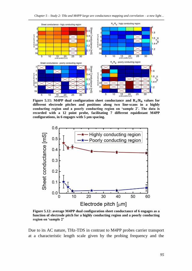
Chapter 5 – Study 2: THz and M4PP large are conductance mapping and correlation – a new light…
95
Figure 5.11: M4PP dual configuration sheet conductance and RA/RB values for
different electrode pitches and positions along two line-scans in a highly
conducting region and a poorly conducting region on ‘sample 2’. The data is
recorded with a 12 point probe, facilitating 7 different equidistant M4PP
configurations, in 6 engages with 5 µm spacing.
Figure 5.12: average M4PP dual configuration sheet conductance of 6 engages as a
function of electrode pitch for a highly conducting region and a poorly conducting
region on ‘sample 2’
Due to its AC nature, THz-TDS in contrast to M4PP probes carrier transport
at a characteristic length scale given by the probing frequency and the
Chapter 5 – Study 2: THz and M4PP large are conductance mapping and correlation – a new light…
96
material diffusion constant67,136
. Under the assumption of a diffusive
transport regime, this characteristic length scale can be estimated as
,2
DL
f (5.2)
2
,2 2
F s F
s
E ED
n e e
(5.3)
where L is the characteristic length scale, D is the diffusion constant, f is the
frequency, EF is the Fermi level, ns is the carrier density, e is the elementary
charge, s is the sheet conductance and is the carrier mobility. L is on the
order of 10-8
to 10-7
m (approximately 84 nm and 26 nm at 0.15 and 1.5 THz,
respectively, as indicated in Figure 5.4) for an estimated D = (66±15) cm2/s
(corresponding to a Hall mobility of 2 2(3.3 0.7) 10 cm /Vs measured
in a high conductance area and thus an estimated Fermi level of
(0.40 0.04) eVFE ). This means that the measured THz conductance
reflects the spatially averaged nanoscopic conductance of the graphene film,
and is thus far less affected by the microscopic defects found to greatly
affect the M4PP conductance of this graphene film. The THz conductance is,
however, highly sensitive to defects on the nanoscopic scale. The THz
conductance spectrum for sample 2, shown in Figure 5.4(a), which displays
no significant frequency dependence is an indication of an electrically
homogeneous and continuous film on the scale from a few tens of nm to
around a hundred nm.
The behavior of the graphene film as a continuous sheet on the nanoscopic
probing length scale of THz conductance measurements in contrast to its
behavior as a highly defected sheet on the microscopic transport length scale
of the M4PP conductance measurements is the most obvious explanation for
the discrepancy between THz-TDS and M4PP sheet conductance values.
These two results in combination suggest that this sample is electrically
continuous on the few tens to around a hundred nanometer length scale
while dominated in its micro-scale electrical response by a high density of
insulating defects of dimensions similar to the M4PP electrode pitch of 10
m. The origin of such insulating micro-scale defects could be damage
occurring during the transfer process as well as incomplete growth coverage
or crystal growth defects, as certain graphene crystal domain boundaries
have been shown to produce perfectly reflecting interfaces for low energy
Chapter 5 – Study 2: THz and M4PP large are conductance mapping and correlation – a new light…
97
charge carriers64
. For sample 2, however, it is likely that the defects are
transfer-related as the typical domain size obtained with the low partial
pressure growth procedure is around 200 m63,171
. This conclusion is
supported by the fact that the pixels shown as blue dots in Figure 5.9(a) and
(b) with= s,M4PP/s,THz > 0.4, i.e. pixels where M4PP sheet conductance is
most substantially lowered by micro-scale defects, tend to cluster around
holes in the film and regions of very distinct optically visible transfer
damage.-Raman mapping results also support this notion, as they indicate
strong correlation between M4PP and THz-TDS sheet conductance and
graphene coverage.
5.6 Conclusions
In summary direct, quantitative mapping of the sheet conductance of cm-
scale CVD graphene films by M4PP and non-contact THz-TDS was
demonstrated, facilitating characterization of the electrical uniformity of
large area graphene films. It was shown that the THz-TDS measurement
probes the spatially averaged nanoscopic transport properties of the graphene
film while the M4PP microscopic transport measurement is highly sensitive
to micro-scale defects. The THz conductance measurement thus provides the
natural upper limit for M4PP sheet conductance measurement in graphene. A
correlation analysis of quantitative M4PP and THz-TDS mappings of the
sheet conductance of a large area CVD graphene film reveals that the film is
electrically continuous on the characteristic length scale associated with the
THz-TDS measurement of a few tens of nanometers to a few hundred
nanometers, while its micro-scale sheet conductance probed by M4PP, is
dominated by a high density of insulating defects with dimensions similar to
the electrode pitch of 10 m. µ-Raman mapping of the sample shows that
both M4PP and THz-TDS conductances are strongly correlated to the
graphene coverage, indicating that the microscopic insulating defects
originate from the transfer process or from incomplete growth coverage.
Both the M4PP and the THz-TDS conductance mapping techniques, as
demonstrated and quantified here for cm-size graphene areas, are
immediately scalable to full wafer dimensions and straightforwardly
extended to work on a wide range of substrates, including thin, flexible
polymers and doped semiconductors. A THz-TDS scan time of less than 1
minute (1 ms/pixel) for a 4” wafer is technologically possible today (5
s/pixel for M4PP), making this technique particularly promising as a high-
Chapter 5 – Study 2: THz and M4PP large are conductance mapping and correlation – a new light…
98
throughput, non-contact metrology tool for mapping of the spatially
averaged nanoscopic conductance on wafer-scale graphene. In a wider
perspective, the application of THz-TDS for nanoscopic conductance
mapping can be extended to various electrically non-uniform or structured
materials, such as for instance polymer-based, polycrystalline or structured
photovoltaic materials. In addition, the combination of M4PP and THz-TDS
offers the exciting potential of directly mapping both the Hall mobility135
and
the carrier scattering time156,182
across wafer-scale areas of graphene films,
without need for post-process patterning.
In emerging applications requiring up to square meter dimensions of
graphene (electronics, displays, touch screens, photovoltaic applications),
rapid, quantitative, contact-free inline characterization of the conductance is
of vital importance. The results presented here may help pave the way
towards that technologically important goal.
Chapter 5 – Study 2: THz and M4PP large are conductance mapping and correlation – a new light…
99
Chapter 5 – Study 2: THz and M4PP large are conductance mapping and correlation – a new light…
100
101
6 Study 3: Gated THz conductance
mapping for non-contact graphene
mobility mapping
Graphene2 is finding its uses in an increasing number of commercially
oriented applications55,56,144,148,183–186
and industrial development
environments57,59,187
, motivated by its combination of exceptional electronic,
optical, and mechanical properties as well as the increasing availability of
synthesized large-area graphene films. In particular, there is a profound
interest in the commercial adaptation of large-area graphene of high
electrical quality for electronic applications, including terahertz (THz)
electronics as well as transparent, flexible, and durable electrodes for
graphene-based touch-sceens and solar cells188
.
There have been several demonstrations of the unique suitability of terahertz
time-domain spectroscopy for rapid and contact-free conductance
measurements of large-area graphene122,123,125,
including the work presented
in this thesis. Rapid data acquisition and non-contact nature of the technique
facilitates practical implementations of in-line spatial mapping of graphene
sheet conductance on a large scale121,129,189
. For typical electronic
applications190
, however, the conductance of a graphene film in itself gives
an insufficient picture in terms of its expected performance, necessitating an
insight into more fundamental material properties. For many scientific as
well as commercial applications, the carrier mobility, , and the carrier
density, ns, are essential figures of merit14,54
, and the most straightforward
way to obtain information on and ns is through the electric field effect,
which requires a variable gate potential. In contact-based electrical
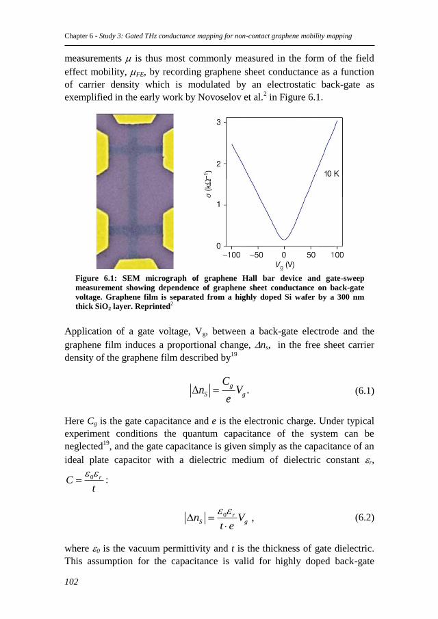
Chapter 6 - Study 3: Gated THz conductance mapping for non-contact graphene mobility mapping
102
measurements is thus most commonly measured in the form of the field
effect mobility, FE, by recording graphene sheet conductance as a function
of carrier density which is modulated by an electrostatic back-gate as
exemplified in the early work by Novoselov et al.2 in Figure 6.1.
Figure 6.1: SEM micrograph of graphene Hall bar device and gate-sweep
measurement showing dependence of graphene sheet conductance on back-gate
voltage. Graphene film is separated from a highly doped Si wafer by a 300 nm
thick SiO2 layer. Reprinted2
Application of a gate voltage, Vg, between a back-gate electrode and the
graphene film induces a proportional change, ns, in the free sheet carrier
density of the graphene film described by19
.g
S g
Cn V
e (6.1)
Here Cg is the gate capacitance and e is the electronic charge. Under typical
experiment conditions the quantum capacitance of the system can be
neglected19
, and the gate capacitance is given simply as the capacitance of an
ideal plate capacitor with a dielectric medium of dielectric constant r,
0 rCt
:
0 ,rS gn V
t e
(6.2)
where 0 is the vacuum permittivity and t is the thickness of gate dielectric.
This assumption for the capacitance is valid for highly doped back-gate
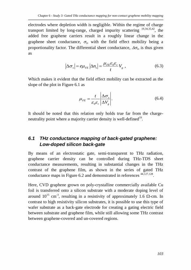
Chapter 6 - Study 3: Gated THz conductance mapping for non-contact graphene mobility mapping
103
electrodes where depletion width is negligible. Within the regime of charge
transport limited by long-range, charged impurity scattering 19,34,35,42
, the
added free graphene carriers result in a roughly linear change in the
graphene sheet conductance, s, with the field effect mobility being a
proportionality factor. The differential sheet conductance, s, is thus given
as
0 ,FE rs FE s ge n V
t
(6.3)
Which makes it evident that the field effect mobility can be extracted as the
slope of the plot in Figure 6.1 as
0
.sFE
r g
t
V
(6.4)
It should be noted that this relation only holds true far from the charge-
neutrality point where a majority carrier density is well-defined19
.
6.1 THz conductance mapping of back-gated graphene:
Low-doped silicon back-gate
By means of an electrostatic gate, semi-transparent to THz radiation,
graphene carrier density can be controlled during THz-TDS sheet
conductance measurements, resulting in substantial changes in the THz
contrast of the graphene film, as shown in the series of gated THz
conductance maps in Figure 6.2 and demonstrated in references 44,127,128
.
Here, CVD graphene grown on poly-crystalline commercially available Cu
foil is transferred onto a silicon substrate with a moderate doping level of
around 1015
cm-3
, resulting in a resistivity of approximately 1.6 -cm. In
contrast to high resistivity silicon substrates, it is possible to use this type of
wafer substrate as a back-gate electrode for creating a gating electric field
between substrate and graphene film, while still allowing some THz contrast
between graphene-covered and un-covered regions.
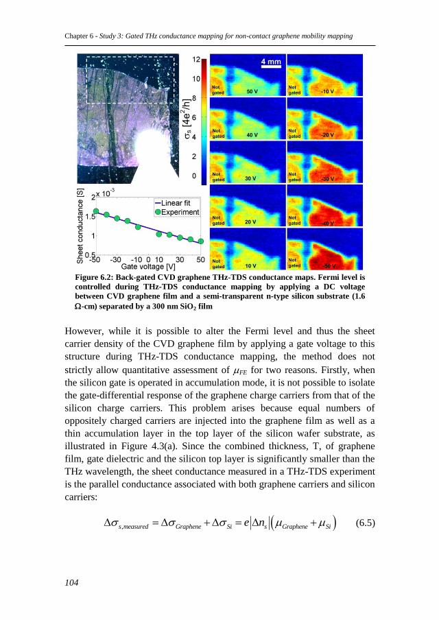
Chapter 6 - Study 3: Gated THz conductance mapping for non-contact graphene mobility mapping
104
Figure 6.2: Back-gated CVD graphene THz-TDS conductance maps. Fermi level is
controlled during THz-TDS conductance mapping by applying a DC voltage
between CVD graphene film and a semi-transparent n-type silicon substrate (1.6
-cm) separated by a 300 nm SiO2 film
However, while it is possible to alter the Fermi level and thus the sheet
carrier density of the CVD graphene film by applying a gate voltage to this
structure during THz-TDS conductance mapping, the method does not
strictly allow quantitative assessment of FE for two reasons. Firstly, when
the silicon gate is operated in accumulation mode, it is not possible to isolate
the gate-differential response of the graphene charge carriers from that of the
silicon charge carriers. This problem arises because equal numbers of
oppositely charged carriers are injected into the graphene film as well as a
thin accumulation layer in the top layer of the silicon wafer substrate, as
illustrated in Figure 4.3(a). Since the combined thickness, T, of graphene
film, gate dielectric and the silicon top layer is significantly smaller than the
THz wavelength, the sheet conductance measured in a THz-TDS experiment
is the parallel conductance associated with both graphene carriers and silicon
carriers:
,s measured Graphene Si s Graphene Sie n (6.5)
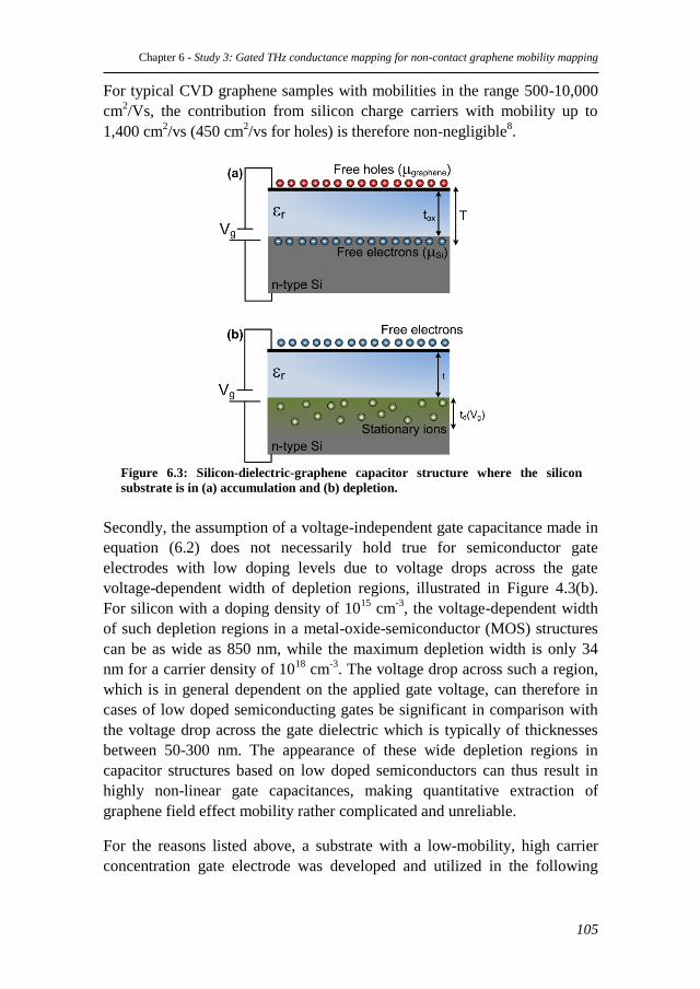
Chapter 6 - Study 3: Gated THz conductance mapping for non-contact graphene mobility mapping
105
For typical CVD graphene samples with mobilities in the range 500-10,000
cm2/Vs, the contribution from silicon charge carriers with mobility up to
1,400 cm2/vs (450 cm
2/vs for holes) is therefore non-negligible
8.
Figure 6.3: Silicon-dielectric-graphene capacitor structure where the silicon
substrate is in (a) accumulation and (b) depletion.
Secondly, the assumption of a voltage-independent gate capacitance made in
equation (6.2) does not necessarily hold true for semiconductor gate
electrodes with low doping levels due to voltage drops across the gate
voltage-dependent width of depletion regions, illustrated in Figure 4.3(b).
For silicon with a doping density of 1015
cm-3
, the voltage-dependent width
of such depletion regions in a metal-oxide-semiconductor (MOS) structures
can be as wide as 850 nm, while the maximum depletion width is only 34
nm for a carrier density of 1018
cm-3
. The voltage drop across such a region,
which is in general dependent on the applied gate voltage, can therefore in
cases of low doped semiconducting gates be significant in comparison with
the voltage drop across the gate dielectric which is typically of thicknesses
between 50-300 nm. The appearance of these wide depletion regions in
capacitor structures based on low doped semiconductors can thus result in
highly non-linear gate capacitances, making quantitative extraction of
graphene field effect mobility rather complicated and unreliable.
For the reasons listed above, a substrate with a low-mobility, high carrier
concentration gate electrode was developed and utilized in the following
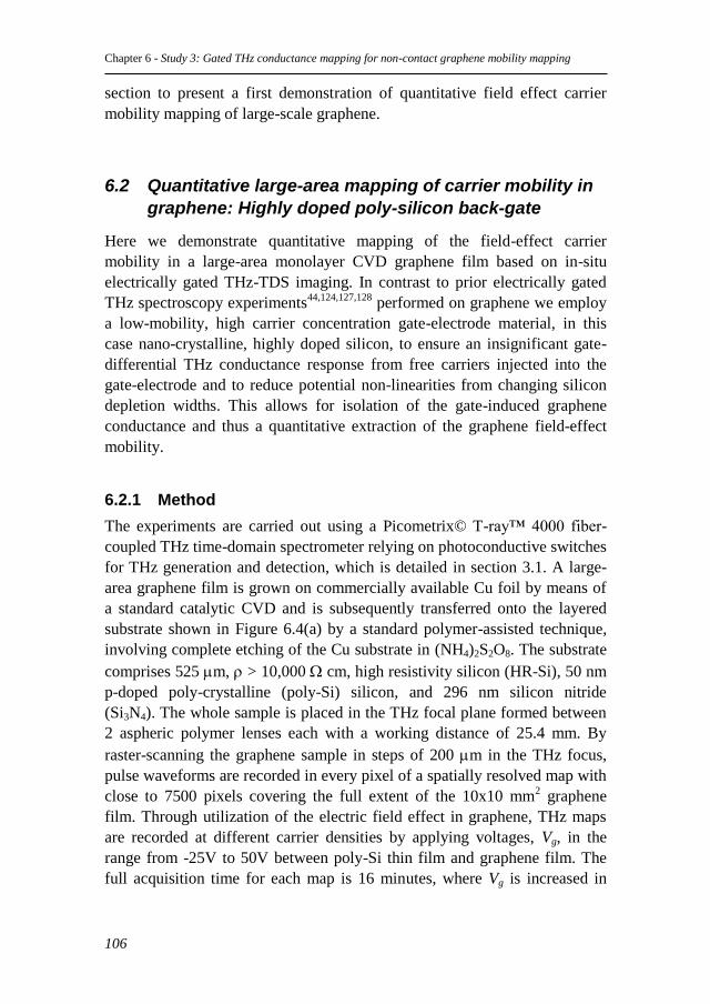
Chapter 6 - Study 3: Gated THz conductance mapping for non-contact graphene mobility mapping
106
section to present a first demonstration of quantitative field effect carrier
mobility mapping of large-scale graphene.
6.2 Quantitative large-area mapping of carrier mobility in
graphene: Highly doped poly-silicon back-gate
Here we demonstrate quantitative mapping of the field-effect carrier
mobility in a large-area monolayer CVD graphene film based on in-situ
electrically gated THz-TDS imaging. In contrast to prior electrically gated
THz spectroscopy experiments44,124,127,128
performed on graphene we employ
a low-mobility, high carrier concentration gate-electrode material, in this
case nano-crystalline, highly doped silicon, to ensure an insignificant gate-
differential THz conductance response from free carriers injected into the
gate-electrode and to reduce potential non-linearities from changing silicon
depletion widths. This allows for isolation of the gate-induced graphene
conductance and thus a quantitative extraction of the graphene field-effect
mobility.
6.2.1 Method
The experiments are carried out using a Picometrix© T-ray™ 4000 fiber-
coupled THz time-domain spectrometer relying on photoconductive switches
for THz generation and detection, which is detailed in section 3.1. A large-
area graphene film is grown on commercially available Cu foil by means of
a standard catalytic CVD and is subsequently transferred onto the layered
substrate shown in Figure 6.4(a) by a standard polymer-assisted technique,
involving complete etching of the Cu substrate in (NH4)2S2O8. The substrate
comprises 525 m, > 10,000 cm, high resistivity silicon (HR-Si), 50 nm
p-doped poly-crystalline (poly-Si) silicon, and 296 nm silicon nitride
(Si3N4). The whole sample is placed in the THz focal plane formed between
2 aspheric polymer lenses each with a working distance of 25.4 mm. By
raster-scanning the graphene sample in steps of 200 m in the THz focus,
pulse waveforms are recorded in every pixel of a spatially resolved map with
close to 7500 pixels covering the full extent of the 10x10 mm2 graphene
film. Through utilization of the electric field effect in graphene, THz maps
are recorded at different carrier densities by applying voltages, Vg, in the
range from -25V to 50V between poly-Si thin film and graphene film. The
full acquisition time for each map is 16 minutes, where Vg is increased in
Chapter 6 - Study 3: Gated THz conductance mapping for non-contact graphene mobility mapping
107
discrete steps of 5V between each map, resulting in an average gate voltage
sweep rate of 0.3125 V/min.
Figure 6.4: a) Schematic of sample consisting of large-area monolayer CVD
graphene film residing on layered substrate comprising 525 mm HR-Si, 50 nm
boron-doped poly-crystalline silicon with n ≈ 1018 cm-3, and 300 nm Si3N4. Au
contacts are used for contacting the graphene film and the poly-crystalline silicon
film. (b) Time-domain waveforms of THz pulses transmitted through a bare HR-Si
substrate and a layered HR-Si/poly-Si/Si3N4 substrate (c) Amplitude transmission
coefficient and phase-shift for poly-Si and Si3N4 films. The THz response of the
thin films is found to be negligible.
The THz response of the poly-Si and Si3N4 films was characterized by
performing transmission measurements on a bare HR-Si substrate as well as
the layered HR-Si/poly-Si/Si3N4 structure, as shown in Figure 6.4(b). It was
found that the THz response of the poly-Si and Si3N4 films is negligible, as
also evidenced by the frequency-independent transmission of 100%, shown
in Figure 6.4(c). The 2-point contact DC sheet conductance of the poly-Si
thin film was also measured at a value of s=0.03 mS, which is at the limit of
sensitivity of the spectrometer. The 2-point sheet conductance value is
Chapter 6 - Study 3: Gated THz conductance mapping for non-contact graphene mobility mapping
108
consistent with an expected carrier mobility191
of 40 cm2/Vs and carrier
density of 1018
cm-3
, as measured by secondary ion mass spectroscopy
profiling. The phase-shift of 2 degrees, seen in Figure 6.4(c), is attributed to
slight differences in HR-Si substrate thickness between the positions of the
reference and sample measurements. The THz response of poly-Si and Si3N4
layers are therefore neglected in the data analysis. Finally, contacts to poly-
Si thin film and contacts for a subsequently transferred CVD graphene film
is defined by electron-beam deposition of 5 nm Ti and 100 nm Au through
an aluminium shadow mask.
6.2.2 Substrate fabrication
As described above, the utilization of a back-gate material combining a
sufficiently low carrier mobility relative to that of CVD graphene and a
carrier density high enough to suppress the impact of a voltage-dependent
depletion width on the gate capacitance of the system is essential for
quantitative extraction of field effect mobility in electrically gated THz-TDS
studies of graphene. In addition, a suitable substrate also has to provide a
useful contrast between graphene-covered and non-graphene-covered areas.
In practical terms for transmission THz-TDS measurements, this requires
that the total sheet conductance of the substrate is kept low enough that a
substantial amount of THz radiation is transmitted through the substrate.
Since no off-the-shelf substrates offer the combination of low mobility, high
carrier density and low total sheet conductance, substrates were designed and
fabricated specifically for this purpose. To keep the sheet conductance of the
substrate low, while allowing the use of a high carrier density gate material,
an approach was chosen where a deposited thin film is used as back gate. To
meet the requirements of low carrier mobility and high carrier density, a
boron-doped chemical vapor deposited poly-crystalline silicon thin film was
chosen, as it yields a carrier mobility of less than 40 cm2/Vs
191 and
facilitates high doping densities.
The entire fabrication process is outlined in Figure 6.5. The CVD process
that was used introduces 80 sccm of SiH4 and 7 sccm of B2H6 during low
pressure chemical vapor deposition at 620o C for in-growth doping to a
carrier density of 1018
cm-3
. Using this method, 50 nm thick boron-doped
poly-crystalline silicon films were deposited on high resistivity double-side-
polished silicon wafers ( ρ 10,000 Ω cm ), resulting in a sheet
conductance of the thin film of s=0.03 mS. As shown in Figure 6.4(b) and
(c), this results in negligible absorption and reflection of THz radiation. The
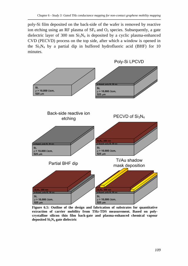
Chapter 6 - Study 3: Gated THz conductance mapping for non-contact graphene mobility mapping
109
poly-Si film deposited on the back-side of the wafer is removed by reactive
ion etching using an RF plasma of SF6 and O2 species. Subsequently, a gate
dielectric layer of 300 nm Si3N4 is deposited by a cyclic plasma-enhanced
CVD (PECVD) process on the top side, after which a window is opened in
the Si3N4 by a partial dip in buffered hydrofluoric acid (BHF) for 10
minutes.
Figure 6.5: Outline of the design and fabrication of substrates for quantitative
extraction of carrier mobility from THz-TDS measurement. Based on poly-
crystalline silicon thin film back-gate and plasma-enhanced chemical vapour
deposited Si3N4 gate dielectric
Chapter 6 - Study 3: Gated THz conductance mapping for non-contact graphene mobility mapping
110
6.2.3 Results and Discussion
THz maps of the CVD graphene film were recorded at 15 different gate
voltages between -25V and 50V, as shown in Figure 6.6(a) where the data is
represented by images showing the transmitted THz power. Since the CVD
graphene film is heavily p-doped, most likely due to exposure to the
(NH4)2S2O8 Cu etchant62
, the conductance and therefore the THz response of
the graphene film are lowest in the Vg = 35V THz map.
The differential gate-induced sheet conductance of the graphene film was
extracted in each pixel of the THz maps based on its direct relation, shown in
equation(6.7), to the complex-valued transmission coefficient, T .
Equation (6.7) is derived from Fresnel coefficients for the boundaries in the
sample geometry, which is modeled as an infinitely thin conducting surface
of sheet conductance, s 94,119 on a thick HR-Si dielectric medium
with refractive index nSi=3.417133
. The complex transmission function is
calculated as the ratio of the Fourier transform of the transmitted THz
waveform, NE , to that of the corresponding pixel in the Vg = 35 V map,
35VE .
35 0
1( ) .
1
N Si
V Si s
E nT
E n Z
(6.6)
From this relation it follows that the differential sheet conductance is
0
111 ,
( )
Sis Si
nn
Z T
(6.7)
where Z0 = 377 is the vacuum impedance. Figure 6.6(b) shows an example
of the extracted s spectrum from the central region of the graphene
film with low THz transmission. The gate-induced THz sheet conductance
exhibits a constant real part of the conductance with magnitude varying with
gate voltage and a constant imaginary part of the conductance, which is
generally close to zero in the accessible frequency range of 0.15-1.4 THz.
This is consistent with a Drude conductance response, which has been
reported for graphene in numerous prior investigations44,122–124,126–128
.
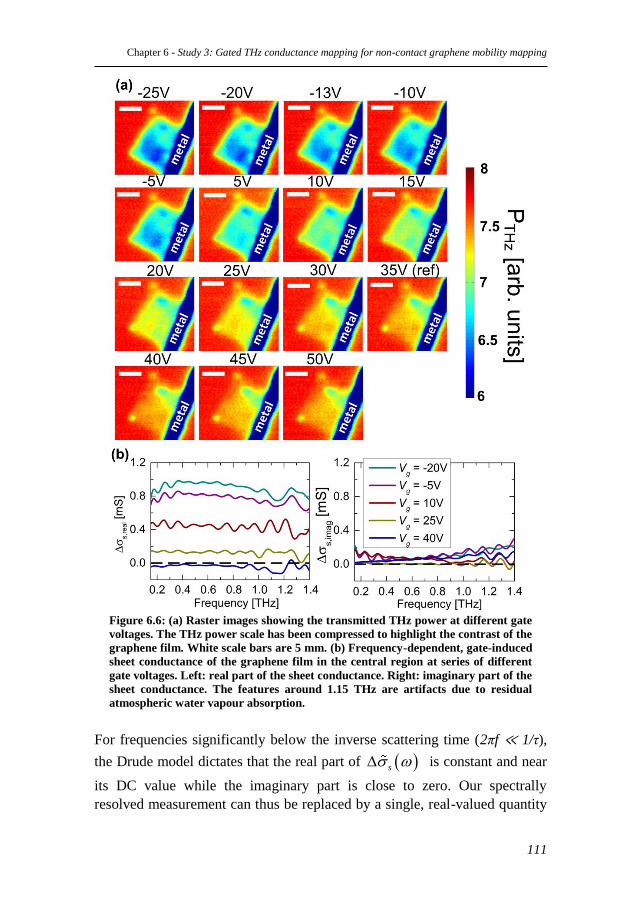
Chapter 6 - Study 3: Gated THz conductance mapping for non-contact graphene mobility mapping
111
Figure 6.6: (a) Raster images showing the transmitted THz power at different gate
voltages. The THz power scale has been compressed to highlight the contrast of the
graphene film. White scale bars are 5 mm. (b) Frequency-dependent, gate-induced
sheet conductance of the graphene film in the central region at series of different
gate voltages. Left: real part of the sheet conductance. Right: imaginary part of the
sheet conductance. The features around 1.15 THz are artifacts due to residual
atmospheric water vapour absorption.
For frequencies significantly below the inverse scattering time (2πf ≪ 1/τ),
the Drude model dictates that the real part of s is constant and near
its DC value while the imaginary part is close to zero. Our spectrally
resolved measurement can thus be replaced by a single, real-valued quantity
Chapter 6 - Study 3: Gated THz conductance mapping for non-contact graphene mobility mapping
112
reflecting the gate-induced DC conductance. In Figure 6.7 we have used this
approach to form spatial maps of the gate-induced graphene sheet
conductance, represented by the average value of Re s between
0.5-0.9 THz, from here on referred to as s. The evolution of s with
varying Vg in the series of images in Figure 6.7 is a result of the electric field
effect in graphene and thus provides vital information on the carrier mobility
in the film. Figure 6.8(a) shows s as a function of Vg for 3 distinct
positions of the mapped area with highly conducting graphene, less
conducting graphene, and no graphene coverage. In contrast to recent back-
gated THz spectroscopy investigations of CVD graphene44,127,128
, our
measurement of s shows a linear dependence on the applied gate voltage
in the range from Vg = -25V to Vg = 30V with different slopes throughout the
extent of the graphene film reflecting the local field-effect mobility. This
observation is found to be representative throughout the graphene film area.
The linear dependence of s on Vg is expected for graphene films where
long-range, charged impurity scattering dominates over short-range neutral
defect scattering19,41
, and typically observed in DC transport measurements
of samples with field effect mobility < 10.000 cm2/Vs
2,32,36. In DC
transport measurements, a sub-linear regime is normally only observed in
ultra-clean exfoliated graphene flakes deposited on substrates with very low
interaction with the graphene layer32,192
. For gate voltages 30V < Vg < 50V a
plateau with close to constant s is found, which is consistent with a gate-
independent charge-puddle regime near the charge-neutrality-point (CNP) in
graphene19
. Application of a gate voltage, Vg, between the poly-Si thin film
and the graphene film induces a proportional change in the free carrier
density, ns, in the poly-Si and graphene films, as described by equation(6.8)
. Within the regime of long-range, charged impurity scattering, the added
free graphene carriers result in a roughly linear change in the graphene sheet
conductance, s, with the field effect mobility being a proportionality
factor. The differential sheet conductance, s, of the graphene film is thus
described by the relations19
:
0 ,
g SiNS g g
Cn V V
e t e
(6.8)
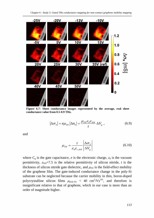
Chapter 6 - Study 3: Gated THz conductance mapping for non-contact graphene mobility mapping
113
Figure 6.7: Sheet conductance images represented by the average, real sheet
conductance value from 0.5-0.9 THz.
0 ,FE SiNS FE S ge n V
t
(6.9)
and
0 ,
SFE
r SiN g
t
V
(6.10)
where Cg is the gate capacitance, e is the electronic charge, 0 is the vacuum
permittivity, SiN=7.5 is the relative permittivity of silicon nitride, t is the
thickness of silicon nitride gate dielectric, and FE is the field-effect mobility
of the graphene film. The gate-induced conductance change in the poly-Si
substrate can be neglected because the carrier mobility in thin, boron-doped
polycrystalline silicon films poly-Si, < 40 cm2/Vs
191, and therefore is
insignificant relative to that of graphene, which in our case is more than an
order of magnitude higher.
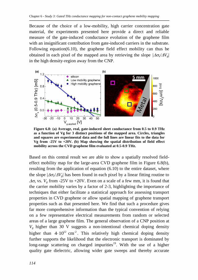
Chapter 6 - Study 3: Gated THz conductance mapping for non-contact graphene mobility mapping
114
Because of the choice of a low-mobility, high carrier concentration gate
material, the experiments presented here provide a direct and reliable
measure of the gate-induced conductance evolution of the graphene film
with an insignificant contribution from gate-induced carriers in the substrate.
Following equation(6.10), the graphene field effect mobility can thus be
obtained in each pixel of the mapped area by retrieving the slope |s/Vg|
in the high density-region away from the CNP.
Figure 6.8: (a) Average, real, gate-induced sheet conductance from 0.5 to 0.9 THz
as a function of Vg for 3 distinct positions of the mapped area. Circles, triangles
and squares are experimental data and the full lines are linear fits to the data for
Vg from -25V to +20V. (b) Map showing the spatial distribution of field effect
mobility across the CVD graphene film evaluated at 0.5-0.9 THz.
Based on this central result we are able to show a spatially resolved field-
effect mobility map for the large-area CVD graphene film in Figure 6.8(b),
resulting from the application of equation (6.10) to the entire dataset, where
the slope |s/Vg| has been found in each pixel by a linear fitting routine to
s vs. Vg from -25V to +20V. Even on a scale of a few mm, it is found that
the carrier mobility varies by a factor of 2-3, highlighting the importance of
techniques that either facilitate a statistical approach for assessing transport
properties in CVD graphene or allow spatial mapping of graphene transport
properties such as that presented here. We find that such a procedure gives
far more comprehensive information than the typical convention of relying
on a few representative electrical measurements from random or selected
areas of a large graphene film. The general observation of a CNP position at
Vg higher than 30 V suggests a non-intentional chemical doping density
higher than 12 -24 10 cm . This relatively high chemical doping density
further supports the likelihood that the electronic transport is dominated by
long-range scattering on charged impurities19
. With the use of a higher
quality gate dielectric, allowing wider gate sweeps and thereby accurate
Chapter 6 - Study 3: Gated THz conductance mapping for non-contact graphene mobility mapping
115
observations of the CNP for each pixel, the presented method can be
straightforwardly extended to provide independent probing and spatially
resolved mapping of carrier density and chemical impurity doping density in
large-area graphene films.
It should be noted that the local carrier mobilities obtained in these
measurements are expected to be a slight underestimate of the actual carrier
mobilities of the graphene film. Due to the low gate sweep rate of 0.3125
V/min, water adsorption and trapping of charges in the silicon nitride is
expected to reduce the effective gate voltage significantly193,194
. This issue
may be explored further by a transition to a measurement protocol, where the
gate voltage instead is swept for each raster-position of the sample, allowing
for variation of the gate sweep rate in a range (typically around 1 V/s193,194
)
relevant for the processes leading to gate hysteresis.
We anticipate that such quantitative, non-contact mapping of graphene
carrier mobility will have a significant technological importance for the
advancement of production and implementations of large-area graphene in
commercial electronic applications and that it can contribute to the
fundamental insight into charge carrier dynamics of the graphene solid-state-
system by paving the way for investigations of transport dynamics with
unprecedented statistical basis.
6.2.4 Conclusion
In conclusion, we have presented non-contact, quantitative mapping of
graphene field effect mobility in a 10x10 mm2 large-area CVD film by in-
situ electrically gated THz-TDS measurements. A THz-TDS scan time of
less than 1 min (1 ms/pixel) for a 4” wafer is technologically possible today,
making the presented method immediately scalable to full wafer dimensions.
While THz-TDS is based on an optical characterization, the frequency range
is well below the inverse scattering time of graphene, and thus the
spectroscopically obtained conductance can be directly extrapolated to its
DC value. The technique thus opens up the possibility for assessment of
fundamental electrical transport properties such as carrier mobility and
chemical impurity doping density on basis of large statistical ensembles, or
large-area spatial mapping of carrier mobility and carrier density. Far from
the charge-neutrality-point, our measurements show a linear dependence of
the THz sheet conductance on carrier density, which is a signature of
electrical transport limited by long-range, charged impurity scattering, also
observed in most DC transport measurements on graphene. On a scale of just
Chapter 6 - Study 3: Gated THz conductance mapping for non-contact graphene mobility mapping
116
few mm, we find significant spatial variations of a factor of 2-3 in carrier
mobility, which highlights the importance of techniques that facilitate highly
statistical or spatially resolved approaches for assessing transport properties
in CVD graphene.
Chapter 6 - Study 3: Gated THz conductance mapping for non-contact graphene mobility mapping
117
Chapter 6 - Study 3: Gated THz conductance mapping for non-contact graphene mobility mapping
118
119
7 Conclusions
The main goal of the work presented in this thesis has been to utilize
terahertz time-domain spectroscopy for assessing the terahertz transport
dynamics of graphene charge carriers. Specifically, the efforts have been
directed towards two aspects of terahertz time-domain spectroscopy
measurements on graphene; (1) investigation of the fundamental carrier
transport dynamics at femtosecond to picosecond timescales and (2) the
application of terahertz time-domain spectroscopy to commercially relevant
non-contact, large-area electrical characterization of graphene.
Investigations of chemical vapor deposited graphene films, combining
conventional and ultra-broadband terahertz time-domain spectroscopy,
revealed qualitatively different terahertz transport dynamics in graphene
films grown on poly-crystalline copper foils and single-crystalline copper
(111) substrates. While the terahertz conductance of graphene grown on
single-crystalline copper agreed with predictions of a Drude-type electrical
response in graphene, the terahertz conductance of graphene grown on poly-
crystalline copper foil was found to be distinctly better described by the
Drude-Smith model. This astounding observation was interpreted in the
context of preferential carrier back-scattering on extended electronic barriers
with a characteristic length scale corresponding to the probing length scale
of the AC field on the order of 10-100 nm. Although the cause of such back-
scattering was not experimentally identified, the most likely origin of
partially reflecting electronic barriers on this length scale in CVD graphene
films is crystal domain boundaries in the poly-crystalline CVD graphene
film. Direct and accurate measurement of the carrier scattering time and the
Drude weight in graphene grown on single-crystalline copper allowed
Chapter 7 - Conclusions
120
evaluation of the mean free path, carrier density and carrier mobility within
the framework of diffusive transport limited by long-range scattering on
charged impurities. These results underline the unique potential of ultra-
broadband terahertz time-domain spectroscopy for non-contact measurement
of the nature of conduction and fundamental electrical transport parameters
without need for application of external gating potentials or magnetic fields.
The observed Drude and Drude-Smith spectra imply that the THz
conductance of the films is close to its DC value at frequencies well below
the scattering rate. This was confirmed in experiments, systematically
comparing line scans of terahertz AC and micro four-point probe DC sheet
conductance, based on which full wafer-scale, non-contact mapping of CVD
graphene electrical sheet conductance was demonstrated by terahertz time-
domain spectroscopic imaging. This demonstration shows that THz-TDS can
indeed facilitate the rapid and reliable large-scale measurement of electronic
properties and their uniformity in large-scale graphene, which might be
viewed as a vital requirement for industrial implementation of the material.
The correlation between terahertz AC conductance and micro four-point
probe DC conductance was investigated in detail based on concurrent
conductance mapping by terahertz time-domain spectroscopy and micro
four-point probe measurements in centimeter-scale CVD graphene films. On
the statistical basis of more than 4000 individual electrical conductance
measurements it was found that the micrometer-scale conductance of the
investigated film was dominated by electrical defects on a characteristic
scale on the order of 10 m. Even though the recent ultra-broadband
terahertz spectroscopy results presented in this thesis show presence of
electrical defects also on the nanoscopic scale, the micro four-point probe
microscopic conductance was thus found to be significantly reduced relative
to the terahertz nanoscopic conductance. The terahertz conductance therefore
provides a natural upper limit for the micro four-point probe conductance in
the graphene film.
Finally, large-scale, quantitative, non-contact mapping of field effect
mobility in a 10x10 mm2 CVD graphene film was demonstrated by in-situ
electrically gated terahertz time-domain spectroscopic imaging. Quantitative
extraction of the field effect mobility was enabled by the use of designed and
fabricated substrates with a low-mobility, high-carrier density poly-
crystalline silicon back-gate, which ensures an insignificant gate-induced
conductance response from carriers injected into the gate electrode. Far from
the charge-neutrality-point, the terahertz sheet conductance shows a linear
dependence on carrier density, which is a signature of electrical transport
Chapter 7 - Conclusions
121
limited by long-range, charged impurity scattering, also observed in most
DC transport measurements on graphene. Significant spatial variations in
carrier mobility of a factor of 2-3 was found on a scale of just few
millimeters, highlighting the importance of techniques that facilitate highly
statistical or spatially resolved approaches for assessment of transport
properties in CVD graphene.
Chapter 7 - Conclusions
122
Bibliography
123
8 Bibliography
8.1 List of references
1. Novoselov, K. S. et al. Electric Field Effect in Atomically Thin
Carbon Films. Science (80-. ). 306, 666–669 (2004).
2. Novoselov, K. S. et al. Two-dimensional gas of massless Dirac
fermions in graphene. Nature 438, 197–200 (2005).
3. Zhang, Y., Tan, Y.-W., Stormer, H. L. & Kim, P. Experimental
observation of the quantum Hall effect and Berry’s phase in
graphene. Nature 438, 201–204 LA – en (2005).
4. Ad-hoc-working-group (European commision). Critical raw
materials for the EU - Report of the Ad-hoc Working Group on
defining critical raw materials. 1–84 (2010).
5. De, S. & Coleman, J. N. Are there fundamental limitations on the
sheet resistance and transmittance of thin graphene films? ACS Nano
4, 2713–20 (2010).
6. Hecht, D. S., Hu, L. & Irvin, G. Emerging transparent electrodes
based on thin films of carbon nanotubes, graphene, and metallic
nanostructures. Adv. Mater. 23, 1482–513 (2011).
7. Schwierz, F. Graphene transistors. Nat. Nanotechnol. 5, 487–496
(2010).
Bibliography
124
8. Jacoboni, C., Canali, C., Ottaviani, G. & Alberigi Quaranta, A. A
review of some charge transport properties of silicon. Solid. State.
Electron. 20, 77–89 (1977).
9. Fistul, V. I., Iglitsyn, M. I. & Omelyanovskii, E. M. Mobility of
electrons in germanium strongly doped with arsenic. Sov. Physics-
Solid Sate 4, 784–785 (1962).
10. Jacoboni, C., Nava, F., Canali, C. & Ottaviani, G. Electron drift
velocity and diffusivity in germanium. Phys. Rev. B 24, 1014–1026
(1981).
11. Blakemore, J. S. Semiconducting and other major properties of
gallium arsenide. J. Appl. Phys. 53, R123 (1982).
12. Karataev, V. V., Milvidskii, M. G., Rytova, N. S. & Fistul, V. I.
Compensation in n-type InAs. Sov. Phys. Semicond. 11, 1009–1011
(1977).
13. Dürkop, T., Getty, S. A., Cobas, E. & Fuhrer, M. S. Extraordinary
Mobility in Semiconducting Carbon Nanotubes. Nano Lett. 4, 35–39
(2004).
14. Mayorov, A. S. et al. Micrometer-scale ballistic transport in
encapsulated graphene at room temperature. Nano Lett. 11, 2396–9
(2011).
15. Geim, A. K. & Novoselov, K. S. The rise of graphene. Nat Mater 6,
183–191 (2007).
16. Novoselov, K. S. et al. Two-dimensional atomic crystals. Proc. Natl.
Acad. Sci. 102, 10451–10453 (2005).
17. Charlier, J.-C., Eklund, P. C. & Ferrari, A. C. in Carbon Nanotub.
Adv. Top. Synth. Struct. Prop. Appl. 111, 673–709 (Springer Berlin
Heidelberg, 2008).
18. Castro Neto, A. H., Peres, N. M. R., Novoselov, K. S. & Geim, A. K.
The electronic properties of graphene. Rev. Mod. Phys. 81, 109–162
(2009).
Bibliography
125
19. Das Sarma, S., Adam, S., Hwang, E. H. & Rossi, E. Electronic
transport in two-dimensional graphene. Rev. Mod. Phys. 83, 407–470
(2011).
20. Geim, A. K. & MacDonald, A. H. Graphene: Exploring carbon
flatland. Phys. Today 60, 35–41 (2007).
21. Morozov, S. et al. Giant Intrinsic Carrier Mobilities in Graphene and
Its Bilayer. Phys. Rev. Lett. 100, 016602 (2008).
22. Ferrari, A. C. Raman spectroscopy of graphene and graphite:
Disorder, electron-phonon coupling, doping and nonadiabatic
effects. Solid State Commun. 143, 47–57 (2007).
23. Ferrari, A. C. & Basko, D. M. Raman spectroscopy as a versatile tool
for studying the properties of graphene. Nat. Nanotechnol. 8, 235–46
(2013).
24. Yu, V., Whiteway, E., Maassen, J. & Hilke, M. Raman spectroscopy
of the internal strain of a graphene layer grown on copper tuned by
chemical vapor deposition. Phys. Rev. B 84, (2011).
25. Aleiner, I. L. & Efetov, K. B. Effect of Disorder on Transport in
Graphene. Phys. Rev. Lett. 97, 236801 (2006).
26. Altland, A. Low-Energy Theory of Disordered Graphene. Phys. Rev.
Lett. 97, 236802 (2006).
27. Peres, N. M. R., Guinea, F. & Castro Neto, A. H. Electronic
properties of disordered two-dimensional carbon. Phys. Rev. B 73,
125411 (2006).
28. Tworzydło, J., Trauzettel, B., Titov, M., Rycerz, A. & Beenakker, C.
Sub-Poissonian Shot Noise in Graphene. Phys. Rev. Lett. 96, 246802
(2006).
29. Bardarson, J., Tworzydło, J., Brouwer, P. & Beenakker, C. One-
Parameter Scaling at the Dirac Point in Graphene. Phys. Rev. Lett. 99,
106801 (2007).
30. Kashuba, A. Conductivity of defectless graphene. Phys. Rev. B 78,
085415 (2008).
Bibliography
126
31. Fritz, L., Schmalian, J., Müller, M. & Sachdev, S. Quantum critical
transport in clean graphene. Phys. Rev. B 78, 085416 (2008).
32. Tan, Y.-W. et al. Measurement of Scattering Rate and Minimum
Conductivity in Graphene. Phys. Rev. Lett. 99, 246803 (2007).
33. Martin, J. et al. Observation of electron–hole puddles in graphene
using a scanning single-electron transistor. Nat. Phys. 4, 144–148
(2007).
34. Hwang, E., Adam, S. & Sarma, S. Carrier Transport in Two-
Dimensional Graphene Layers. Phys. Rev. Lett. 98, 186806 (2007).
35. Adam, S., Hwang, E. H., Galitski, V. M. & Das Sarma, S. A self-
consistent theory for graphene transport. Proc. Natl. Acad. Sci. U. S.
A. 104, 18392–7 (2007).
36. Chen, J.-H. et al. Charged-impurity scattering in graphene. Nat. Phys.
4, 377–381 (2008).
37. Meyer, J. C. et al. The structure of suspended graphene sheets.
Nature 446, 60–3 (2007).
38. Mayorov, A. S. et al. How Close Can One Approach the Dirac Point
in Graphene Experimentally? Nano Lett. 12, 4629–34 (2012).
39. Schlom, D. G. & Pfeiffer, L. N. Oxide electronics: Upward mobility
rocks! Nat. Mater. 9, 881–3 (2010).
40. Geim, A. K. & Novoselov, K. S. The rise of graphene. Nat. Mater. 6,
183–91 (2007).
41. Ando, T. Screening Effect and Impurity Scattering in Monolayer
Graphene. J. Phys. Soc. Japan 75, 074716 (2006).
42. Nomura, K. & MacDonald, A. H. Quantum Transport of Massless
Dirac Fermions. Phys. Rev. Lett. 98, 076602 (2007).
43. Peres, N., Lopes dos Santos, J. & Stauber, T. Phenomenological
study of the electronic transport coefficients of graphene. Phys. Rev.
B 76, 073412 (2007).
Bibliography
127
44. Horng, J. et al. Drude conductivity of Dirac fermions in graphene.
Phys. Rev. B 83, 165113 (2011).
45. Petrone, N. et al. Chemical vapor deposition-derived graphene with
electrical performance of exfoliated graphene. Nano Lett. 12, 2751–6
(2012).
46. Tao, L. et al. Uniform Wafer-Scale Chemical Vapor Deposition of
Graphene on Evaporated Cu (111) Film with Quality Comparable to
Exfoliated Monolayer. J. Phys. Chem. C 116, 24068–24074 (2012).
47. Hernandez, Y. et al. High-yield production of graphene by liquid-
phase exfoliation of graphite. Nat. Nanotechnol. 3, 563–8 (2008).
48. Stankovich, S. et al. Synthesis of graphene-based nanosheets via
chemical reduction of exfoliated graphite oxide. Carbon N. Y. 45,
1558–1565 (2007).
49. Li, X. et al. Highly conducting graphene sheets and Langmuir–
Blodgett films. Nat. Nanotechnol. 3, 538–542 (2008).
50. Lotya, M. et al. Liquid phase production of graphene by exfoliation
of graphite in surfactant/water solutions. J. Am. Chem. Soc. 131,
3611–20 (2009).
51. First, P. N. et al. Epitaxial Graphenes on Silicon Carbide. MRS Bull.
35, 296–305 (2011).
52. Emtsev, K. V et al. Towards wafer-size graphene layers by
atmospheric pressure graphitization of silicon carbide. Nat. Mater. 8,
203–7 (2009).
53. Berger, C. et al. Ultrathin Epitaxial Graphite: 2D Electron Gas
Properties and a Route toward Graphene-based Nanoelectronics. J.
Phys. Chem. B 108, 19912–19916 (2004).
54. Li, X. et al. Large-Area Synthesis of High-Quality and Uniform
Graphene Films on Copper Foils. Science (80-. ). 324, 1312 –1314
(2009).
55. Li, X. et al. Transfer of Large-Area Graphene Films for High-
Performance Transparent Conductive Electrodes. Nano Lett. 9, 4359–
4363 (2009).
Bibliography
128
56. Eda, G., Fanchini, G. & Chhowalla, M. Large-area ultrathin films of
reduced graphene oxide as a transparent and flexible electronic
material. Nat. Nanotechnol. 3, 270–4 (2008).
57. Bae, S. et al. Roll-to-roll production of 30-inch graphene films for
transparent electrodes. Nat. Nanotechnol. 5, 574–578 (2010).
58. Hass, J. et al. Structural properties of the multilayer graphene/4H-
SiC(0001¯) system as determined by surface x-ray diffraction. Phys.
Rev. B 75, 214109 (2007).
59. Kim, K. S. et al. Large-scale pattern growth of graphene films for
stretchable transparent electrodes. Nature 457, 706–710 (2009).
60. Li, X. et al. Large-Area Graphene Single Crystals Grown by Low-
Pressure Chemical Vapor Deposition of Methane on Copper. J. Am.
Chem. Soc. 133, 2816–2819 (2011).
61. Li, X. et al. Graphene films with large domain size by a two-step
chemical vapor deposition process. Nano Lett. 10, 4328–34 (2010).
62. Yu, Q. et al. Control and characterization of individual grains and
grain boundaries in graphene grown by chemical vapour deposition.
Nat. Mater. 10, 443–9 (2011).
63. Kim, D. W., Kim, Y. H., Jeong, H. S. & Jung, H.-T. Direct
visualization of large-area graphene domains and boundaries by
optical birefringency. Nat. Nanotechnol. 7, 29–34 (2011).
64. Yazyev, O. V. & Louie, S. G. Electronic transport in polycrystalline
graphene. Nat. Mater. 9, 806–809 (2010).
65. Smith, N. V. Classical generalization of the Drude formula for the
optical conductivity. Phys. Rev. B 64, 155106 (2001).
66. Homes, C. et al. Optical conductivity of the stable icosahedral
quasicrystal Al_{63.5}Cu_{24.5}Fe_{12}. Phys. Rev. Lett. 67,
2694–2696 (1991).
67. Henning, P. F. et al. Infrared Studies of the Onset of Conductivity in
Ultrathin Pb Films. Phys. Rev. Lett. 83, 4880–4883 (1999).
Bibliography
129
68. Cooke, D. G. et al. Transient terahertz conductivity in photoexcited
silicon nanocrystal films. Phys. Rev. B 73, 193311 (2006).
69. Cooke, D. G., Meldrum, A. & Uhd Jepsen, P. Ultrabroadband
terahertz conductivity of Si nanocrystal films. Appl. Phys. Lett. 101,
211107 (2012).
70. Gordon M. Turner, Matthew C. Beard, and & Schmuttenmaer*, C. A.
Carrier Localization and Cooling in Dye-Sensitized Nanocrystalline
Titanium Dioxide. (2002).
71. Beard, M. C. et al. Electronic Coupling in InP Nanoparticle Arrays.
Nano Lett. 3, 1695–1699 (2003).
72. Cheung, K. P. & Auston, D. H. A novel technique for measuring far-
infrared absorption and dispersion. Infrared Phys. 26, 23–27 (1986).
73. Exter, M. van, Fattinger, C. & Grischkowsky, D. Terahertz time-
domain spectroscopy of water vapor. Opt. Lett. 14, 1128 (1989).
74. Winnewisser, G. Spectroscopy in the terahertz region. Vib. Spectrosc.
8, 241–253 (1995).
75. Černe, J. et al. Terahertz Dynamics of Excitons in GaAs/AlGaAs
Quantum Wells. Phys. Rev. Lett. 77, 1131–1134 (1996).
76. Auston, D. H., Cheung, K. P. & Smith, P. R. Picosecond
photoconducting Hertzian dipoles. Appl. Phys. Lett. 45, 284 (1984).
77. Fattinger, C. & Grischkowsky, D. Terahertz beams. Appl. Phys. Lett.
54, 490 (1989).
78. Yang, K. H., Richards, P. L. & Shen, Y. R. Generation of Far-
Infrared Radiation by Picosecond Light Pulses in LiNbO3. Appl.
Phys. Lett. 19, 320 (1971).
79. Hu, B. B., Zhang, X.-C., Auston, D. H. & Smith, P. R. Free-space
radiation from electro-optic crystals. Appl. Phys. Lett. 56, 506 (1990).
80. Nahata, A., Weling, A. S. & Heinz, T. F. A wideband coherent
terahertz spectroscopy system using optical rectification and electro-
optic sampling. Appl. Phys. Lett. 69, 2321 (1996).
Bibliography
130
81. Wu, Q. & Zhang, X.-C. Free-space electro-optic sampling of
terahertz beams. Appl. Phys. Lett. 67, 3523 (1995).
82. Jepsen, P. et al. Detection of THz pulses by phase retardation in
lithium tantalate. Phys. Rev. E 53, R3052–R3054 (1996).
83. Nahata, A., Auston, D. H., Heinz, T. F. & Wu, C. Coherent detection
of freely propagating terahertz radiation by electro-optic sampling.
Appl. Phys. Lett. 68, 150 (1996).
84. Thomson, M. D., Blank, V. & Roskos, H. G. Terahertz white-light
pulses from an air plasma photo-induced by incommensurate two-
color optical fields. Opt. Express 18, 23173–82 (2010).
85. Dai, J., Liu, J. & Zhang, X.-C. Terahertz Wave Air Photonics:
Terahertz Wave Generation and Detection With Laser-Induced Gas
Plasma. IEEE J. Sel. Top. Quantum Electron. 17, 183–190 (2011).
86. Walther, M., Plochocka, P., Fischer, B., Helm, H. & Uhd Jepsen, P.
Collective vibrational modes in biological molecules investigated by
terahertz time-domain spectroscopy. Biopolymers 67, 310–3 (2002).
87. Nuss, M. C. et al. Terahertz time-domain measurement of the
conductivity and superconducting band gap in niobium. J. Appl.
Phys. 70, 2238 (1991).
88. Kaindl, R. A., Carnahan, M. A., Hägele, D., Lövenich, R. & Chemla,
D. S. Ultrafast terahertz probes of transient conducting and insulating
phases in an electron-hole gas. Nature 423, 734–8 (2003).
89. Huber, R., Kaindl, R., Schmid, B. & Chemla, D. Broadband terahertz
study of excitonic resonances in the high-density regime in
GaAs∕AlxGa1−xAs quantum wells. Phys. Rev. B 72, 161314 (2005).
90. Huber, R. et al. How many-particle interactions develop after
ultrafast excitation of an electron-hole plasma. Nature 414, 286–289
(2001).
91. Schall, M., Walther, M. & Uhd Jepsen, P. Fundamental and second-
order phonon processes in CdTe and ZnTe. Phys. Rev. B 64, 094301
(2001).
Bibliography
131
92. Schmuttenmaer, C. A. Exploring dynamics in the far-infrared with
terahertz spectroscopy. Chem. Rev. 104, 1759–79 (2004).
93. Schall, M. & Jepsen, P. U. Photoexcited GaAs surfaces studied by
transient terahertz time-domain spectroscopy. Opt. Lett. 25, 13
(2000).
94. Lui, K. P. H. & Hegmann, F. A. Ultrafast carrier relaxation in
radiation-damaged silicon on sapphire studied by optical-pump–
terahertz-probe experiments. Appl. Phys. Lett. 78, 3478 (2001).
95. Auston, D. H. Picosecond optoelectronic switching and gating in
silicon. Appl. Phys. Lett. 26, 101 (1975).
96. Fattinger, C. & Grischkowsky, D. Point source terahertz optics. Appl.
Phys. Lett. 53, 1480 (1988).
97. Yang, Y., Mandehgar, M. & Grischkowsky, D. Time domain
measurement of the THz refractivity of water vapor. Opt. Express 20,
26208–18 (2012).
98. Lee, Y.-S. Principles of Terahertz Science and Technology.
(Springer, 2008).
99. Jepsen, P. U., Jacobsen, R. H. & Keiding, S. R. Generation and
detection of terahertz pulses from biased semiconductor antennas. J.
Opt. Soc. Am. B 13, 2424–2436 (1996).
100. Cook, D. J. & Hochstrasser, R. M. Intense terahertz pulses by four-
wave rectification in air. Opt. Lett. 25, 1210 (2000).
101. ffler, T., Jacob, F. & Roskos, H. G. Generation of terahertz pulses
by photoionization of electrically biased air. Appl. Phys. Lett. 77, 453
(2000).
102. Xie, X., Dai, J. & Zhang, X.-C. Coherent Control of THz Wave
Generation in Ambient Air. Phys. Rev. Lett. 96, 075005 (2006).
103. Dai, J., Xie, X. & Zhang, X.-C. Detection of Broadband Terahertz
Waves with a Laser-Induced Plasma in Gases. Phys. Rev. Lett. 97,
(2006).
Bibliography
132
104. Matsubara, E., Nagai, M. & Ashida, M. Coherent infrared
spectroscopy system from terahertz to near infrared using air plasma
produced by 10-fs pulses. J. Opt. Soc. Am. B 30, 1627 (2013).
105. Kress, M., Löffler, T., Eden, S., Thomson, M. & Roskos, H. G.
Terahertz-pulse generation by photoionization of air with laser pulses
composed of both fundamental and second-harmonic waves. Opt.
Lett. 29, 1120 (2004).
106. Karpowicz, N. & Zhang, X.-C. Coherent Terahertz Echo of Tunnel
Ionization in Gases. Phys. Rev. Lett. 102, 093001 (2009).
107. Dai, J., Karpowicz, N. & Zhang, X.-C. Coherent Polarization Control
of Terahertz Waves Generated from Two-Color Laser-Induced Gas
Plasma. Phys. Rev. Lett. 103, 023001 (2009).
108. Kim, K.-Y., Glownia, J. H., Taylor, A. J. & Rodriguez, G. Terahertz
emission from ultrafast ionizing air in symmetry-broken laser fields.
Opt. Express 15, 4577 (2007).
109. Kim, K. Y., Taylor, A. J., Glownia, J. H. & Rodriguez, G. Coherent
control of terahertz supercontinuum generation in ultrafast laser–gas
interactions. Nat. Photonics 2, 605–609 (2008).
110. Zhong, H., Karpowicz, N. & Zhang, X.-C. Terahertz emission profile
from laser-induced air plasma. Appl. Phys. Lett. 88, 261103 (2006).
111. You, Y. S., Oh, T. I. & Kim, K. Y. Off-Axis Phase-Matched
Terahertz Emission from Two-Color Laser-Induced Plasma
Filaments. Phys. Rev. Lett. 109, 183902 (2012).
112. Klarskov, P., Strikwerda, A. C., Iwaszczuk, K. & Jepsen, P. U.
Experimental three-dimensional beam profiling and modeling of a
terahertz beam generated from a two-color air plasma. New J. Phys.
15, 075012 (2013).
113. Klarskov, P., Wang, T., Buron, J. D., Strikwerda, A. C. & Jepsen, P.
U. Spatial properties of a terahertz beam generated from a two-color
air plasma. in SPIE Opt. Eng. + Appl. (Razeghi, M., Baranov, A. N.
& Zavada, J. M.) 88460R–88460R–9 (International Society for
Optics and Photonics, 2013). doi:10.1117/12.2023821
Bibliography
133
114. Xie, X., Dai, J. & Zhang, X.-C. Coherent Control of THz Wave
Generation in Ambient Air. Phys. Rev. Lett. 96, (2006).
115. Karpowicz, N. et al. Coherent heterodyne time-domain spectrometry
covering the entire “terahertz gap.”Appl. Phys. Lett. 92, 011131
(2008).
116. Wang, C. S., Chen, J. M., Becker, R. & Zdetsis, A. Second order
Raman spectrum and phonon density of states of silicon. Phys. Lett. A
44, 517–518 (1973).
117. Wei, S. & Chou, M. Phonon dispersions of silicon and germanium
from first-principles calculations. Phys. Rev. B 50, 2221–2226
(1994).
118. Zalkovskij, M. Terahertz time-domain spectroscopy of chalcogenide
glasses and devices for terahertz radiation manipulation. (2013).
119. Glover, R. & Tinkham, M. Conductivity of Superconducting Films
for Photon Energies between 0.3 and 40kTc. Phys. Rev. 108, 243–
256 (1957).
120. Cooke, D. G. Time-resolved terahertz spectroscopy of bulk and
nanoscale semiconductors. 194 LA – English (2006).
121. Tomaino, J. L. et al. Terahertz imaging and spectroscopy of large-
area single-layer graphene. Opt. Express 19, 141–146 (2011).
122. Dawlaty, J. M. et al. Measurement of the optical absorption spectra
of epitaxial graphene from terahertz to visible. Appl. Phys. Lett. 93,
131905–131905–3 (2008).
123. Choi, H. et al. Broadband electromagnetic response and ultrafast
dynamics of few-layer epitaxial graphene. Appl. Phys. Lett. 94,
172102 (2009).
124. Jnawali, G., Rao, Y., Yan, H. & Heinz, T. F. Observation of a
transient decrease in terahertz conductivity of single-layer graphene
induced by ultrafast optical excitation. Nano Lett. 13, 524–30 (2013).
125. Liu, W., Valdés Aguilar, R., Hao, Y., Ruoff, R. S. & Armitage, N. P.
Broadband microwave and time-domain terahertz spectroscopy of
Bibliography
134
chemical vapor deposition grown graphene. J. Appl. Phys. 110,
083510–083510–5 (2011).
126. Li, Z. Q. et al. Dirac charge dynamics in graphene by infrared
spectroscopy. Nat. Phys. 4, 532–535 (2008).
127. Ren, L. et al. Terahertz and Infrared Spectroscopy of Gated Large-
Area Graphene. Nano Lett. 12, 3711–3715 (2012).
128. Maeng, I. et al. Gate-Controlled Nonlinear Conductivity of Dirac
Fermion in Graphene Field-Effect Transistors Measured by Terahertz
Time-Domain Spectroscopy. Nano Lett. 12, 551–555 (2012).
129. Buron, J. D. et al. Graphene Conductance Uniformity Mapping. Nano
Lett. 12, 5074–5081 (2012).
130. Hu, B. et al. Epitaxial growth of large-area single-layer graphene
over Cu(111)/sapphire by atmospheric pressure CVD. Carbon N. Y.
50, 57–65 (2012).
131. Wood, J. D., Schmucker, S. W., Lyons, A. S., Pop, E. & Lyding, J.
W. Effects of polycrystalline cu substrate on graphene growth by
chemical vapor deposition. Nano Lett. 11, 4547–54 (2011).
132. Gao, L., Guest, J. R. & Guisinger, N. P. Epitaxial Graphene on
Cu(111). (2010).
133. Grischkowsky, D. R., Keiding, S., Vanexter, M. & Fattinger, C. Far-
infrared time-domain spectroscopy with terahertz beams of
dielectrics and semiconductors. J. Opt. Soc. Am. B-Optical Phys. 7,
2006–2015 (1990).
134. Dai, J., Zhang, J., Zhang, W. & Grischkowsky, D. Terahertz time-
domain spectroscopy characterization of the far-infrared absorption
and index of refraction of high-resistivity, float-zone silicon. J. Opt.
Soc. Am. B 21, 1379 (2004).
135. Petersen, D. H., Hansen, O., Lin, R. & Nielsen, P. F. Micro-four-
point probe Hall effect measurement method. J. Appl. Phys. 104,
013710–013710–10 (2008).
136. Berger, C. et al. Electronic confinement and coherence in patterned
epitaxial graphene. Science 312, 1191–6 (2006).
Bibliography
135
137. Petersen, C. . et al. Scanning microscopic four-point conductivity
probes. Sensors Actuators A Phys. 96, 53–58 (2002).
138. Petersen, D. H., Hansen, O., Hansen, T. M., Petersen, P. R. E. &
Bøggild, P. Static contact micro four-point probes with <11nm
positioning repeatability. Microelectron. Eng. 85, 1092–1095 (2008).
139. Rymaszewski, R. Relationship between the correction factor of the
four-point probe value and the selection of potential and current
electrodes. J. Phys. E. 2, 170–174 (1969).
140. Thorsteinsson, S. et al. Accurate microfour-point probe sheet
resistance measurements on small samples. Rev. Sci. Instrum. 80,
53902–53910 (2009).
141. Jeon, T.-I. & Grischkowsky, D. Characterization of optically dense,
doped semiconductors by reflection THz time domain spectroscopy.
Appl. Phys. Lett. 72, (1998).
142. Hwang, C. et al. Fermi velocity engineering in graphene by substrate
modification. Sci. Rep. 2, (2012).
143. Němec, H., Kužel, P. & Sundstr m, V. Far-infrared response of free
charge carriers localized in semiconductor nanoparticles. Phys. Rev.
B 79, 115309 (2009).
144. Lin, Y.-M. et al. Wafer-Scale Graphene Integrated Circuit. Science
(80-. ). 332, 1294–1297 (2011).
145. Liao, L. et al. Sub-100 nm Channel Length Graphene Transistors.
Nano Lett. 10, 3952–3956 (2010).
146. Son, Y.-W., Cohen, M. L. & Louie, S. G. Half-metallic graphene
nanoribbons. Nature 444, 347–349 (2006).
147. Matyba, P. et al. Graphene and Mobile Ions: The Key to All-Plastic,
Solution-Processed Light-Emitting Devices. ACS Nano 4, 637–642
(2010).
148. Bao, Q. et al. Atomic-Layer Graphene as a Saturable Absorber for
Ultrafast Pulsed Lasers. Adv. Funct. Mater. 19, 3077–3083 (2009).
Bibliography
136
149. Feng, M., Zhan, H. & Chen, Y. Nonlinear optical and optical limiting
properties of graphene families. Appl. Phys. Lett. 96, 033107–
033107–3 (2010).
150. Gu, T. et al. Regenerative oscillation and four-wave mixing in
graphene optoelectronics. Nat. Photonics 6, 554–559 (2012).
151. Boubanga-Tombet, S. et al. Ultrafast carrier dynamics and terahertz
emission in optically pumped graphene at room temperature. Phys.
Rev. B 85, (2012).
152. Bonaccorso, F., Sun, Z., Hasan, T. & Ferrari, A. C. Graphene
photonics and optoelectronics. Nat. Photonics 4, 611–622 (2010).
153. Sutter, P. W., Flege, J.-I. & Sutter, E. A. Epitaxial graphene on
ruthenium. Nat. Mater. 7, 406–411 (2008).
154. Reina, A. et al. Large Area, Few-Layer Graphene Films on Arbitrary
Substrates by Chemical Vapor Deposition. Nano Lett. 9, 30–35
(2008).
155. Jepsen, P. U., Cooke, D. G. & Koch, M. Terahertz spectroscopy and
imaging – Modern techniques and applications. Laser Photon. Rev. 5,
124–166 (2011).
156. Katzenellenbogen, N. & Grischkowsky, D. Electrical characterization
to 4 THz of N- and P-type GaAs using THz time-domain
spectroscopy. Appl. Phys. Lett. 61, 840 (1992).
157. Sensale-Rodriguez, B. et al. Broadband graphene terahertz
modulators enabled by intraband transitions. Nat. Commun. 3, 780
(2012).
158. Barraza- opez, S., Vanević, M., Kindermann, M. & Chou, M. Y.
Effects of Metallic Contacts on Electron Transport through
Graphene. Phys. Rev. Lett. 104, (2010).
159. Huard, B., Stander, N., Sulpizio, J. A. & Goldhaber-Gordon, D.
Evidence of the role of contacts on the observed electron-hole
asymmetry in graphene. Phys. Rev. B 78, 121402 (2008).
Bibliography
137
160. J. H. Lee, E., Balasubramanian, K., Weitz, R. T., Burghard, M. &
Kern, K. Contact and edge effects in graphene devices. Nat.
Nanotechnol. 3, 486–490 (2008).
161. Khomyakov, P. A., Starikov, A. A., Brocks, G. & Kelly, P. J.
Nonlinear screening of charges induced in graphene by metal
contacts. Phys. Rev. B 82, 115437 (2010).
162. Petersen, D. H. et al. Comparative study of size dependent four-point
probe sheet resistance measurement on laser annealed ultra-shallow
junctions. J. Vac. Sci. Technol. B Microelectron. Nanom. Struct. 26,
362 (2008).
163. Clarysse, T. et al. in (Pawlak, B., Jones, K., Felch, S. & Hane, M.)
912, 197–202 (Materials Research Society, 2006).
164. Clarysse, T. et al. Photovoltage versus microprobe sheet resistance
measurements on ultrashallow structures. J. Vac. Sci. Technol. B
Microelectron. Nanom. Struct. 28, C1C8 (2010).
165. Clarysse, T. et al. Advanced carrier depth profiling on Si and Ge with
micro four-point probe. J. Vac. Sci. Technol. B Microelectron.
Nanom. Struct. 26, 317 (2008).
166. Clarysse, T. et al. On the analysis of the activation mechanisms of
sub-melt laser anneals. Mater. Sci. Eng. B 154–155, 24–30 (2008).
167. Clarysse, T., Eyben, P., Hantschel, T. & Vandervorst, W. Towards
sub-10 nm carrier profiling with spreading resistance techniques.
Mater. Sci. Semicond. Process. 4, 61–66 (2001).
168. Vandervorst, W. USJ metrology : from 0D to 3D analysis. AIP Conf.
Proc. 931, 233–245 (2007).
169. Wang, F., Petersen, D. H., Osterberg, F. W. & Hansen, O. Accuracy
of micro four-point probe measurements on inhomogeneous samples:
A probe spacing dependence study. in 2009 17th Int. Conf. Adv.
Therm. Process. Semicond. 1–6 (IEEE, 2009).
doi:10.1109/RTP.2009.5373449
170. Klarskov, M. B. et al. Fast and direct measurements of the electrical
properties of graphene using micro four-point probes.
Nanotechnology 22, 445702 (2011).
Bibliography
138
171. Sun, J. et al. Low Partial Pressure Chemical Vapor Deposition of
Graphene on Copper. IEEE Trans. Nanotechnol. 11, 255–260 (2012).
172. Sun, J., Lindvall, N., Cole, M. T., Teo, K. B. K. & Yurgens, A.
Large-area uniform graphene-like thin films grown by chemical
vapor deposition directly on silicon nitride. Appl. Phys. Lett. 98,
252103–252107 (2011).
173. Sun, J., Cole, M. T., Lindvall, N., Teo, K. B. K. & Yurgens, A.
Noncatalytic chemical vapor deposition of graphene on high-
temperature substrates for transparent electrodes. Appl. Phys. Lett.
100, 22102–22103 (2012).
174. Van Der Pauw, L. J. A method of measuring the resistivity and Hall
coefficient on lamellae of arbitrary shape. 20, 220–224 (1958).
175. Petersen, D. H. et al. Review of electrical characterization of ultra-
shallow junctions with micro four-point probes. J. Vac. Sci. Technol.
B Microelectron. Nanom. Struct. 28, C1C27 (2010).
176. Jepsen, P. U. & Fischer, B. Dynamic range in terahertz time-domain
transmission and reflectionspectroscopy. Opt. Lett. 30, 29–31 (2005).
177. Mak, K. F. et al. Measurement of the Optical Conductivity of
Graphene. Phys. Rev. Lett. 101, 196405 (2008).
178. Nair, R. R. et al. Fine Structure Constant Defines Visual
Transparency of Graphene. Science (80-. ). 320, 1308–1308 (2008).
179. Koon, D. W. & Knickerbocker, C. J. What do you measure when you
measure resistivity? Rev. Sci. Instrum. 63, 207–210 (1992).
180. Herring, C. Effect of Random Inhomogeneities on Electrical and
Galvanomagnetic Measurements. J. Appl. Phys. 31, 1939–1953
(1960).
181. Petersen, D. H. et al. High precision micro-scale Hall effect
characterization method using in-line micro four-point probes. in
16th IEEE Int. Conf. Adv. Therm. Process. Semicond. 2008. RTP
2008 251 –256 (IEEE, 2008). doi:10.1109/RTP.2008.4690563
Bibliography
139
182. Cooke, D. G., Krebs, F. C. & Jepsen, P. U. Direct Observation of
Sub-100 fs Mobile Charge Generation in a Polymer-Fullerene Film.
Phys. Rev. Lett. 108, 056603 (2012).
183. Su, F.-Y. et al. Flexible and planar graphene conductive additives for
lithium-ion batteries. J. Mater. Chem. 20, 9644 (2010).
184. Liao, L. et al. High-speed graphene transistors with a self-aligned
nanowire gate. Nature 467, 305–308 (2010).
185. Lin, Y.-M. et al. Operation of Graphene Transistors at Gigahertz
Frequencies. Nano Lett. 9, 422–426 (2009).
186. Xia, F., Mueller, T., Lin, Y., Valdes-Garcia, A. & Avouris, P.
Ultrafast graphene photodetector. Nat. Nanotechnol. 4, 839–843
(2009).
187. www.investorintel.com. Game Changer: Grafoid’s new patent-
pending MesoGrafTM
technology sets the standard for high-energy-
density graphene -.
188. Novoselov, K. S. et al. A roadmap for graphene. Nature 490, 192–
200 (2012).
189. Paul, M. J. et al. Terahertz imaging of inhomogeneous
electrodynamics in single-layer graphene embedded in dielectrics.
Appl. Phys. Lett. 101, 091109 (2012).
190. Avouris, P. & Xia, F. Graphene applications in electronics and
photonics. MRS Bull. 37, 1225–1234 (2012).
191. Kamins, T. I. Hall Mobility in Chemically Deposited Polycrystalline
Silicon. J. Appl. Phys. 42, 4357 (1971).
192. Dean, C. R. et al. Boron nitride substrates for high-quality graphene
electronics. Nat. Nanotechnol. 5, 722–6 (2010).
193. Wang, H., Wu, Y., Cong, C., Shang, J. & Yu, T. Hysteresis of
electronic transport in graphene transistors. ACS Nano 4, 7221–8
(2010).
194. Kalon, G., Jun Shin, Y., Giang Truong, V., Kalitsov, A. & Yang, H.
The role of charge traps in inducing hysteresis: Capacitance–voltage
Bibliography
140
measurements on top gated bilayer graphene. Appl. Phys. Lett. 99,
083109 (2011).
Bibliography
141
8.2 List of Publications
8.2.1 Peer reviewed Journal publications
i. Jonas Due Buron, Dirch Hjorth Petersen, Peter Bøggild, David G.
Cooke, Michael Hilke, Jie Sun, Eric Whiteway, Peter F. Nielsen,
Ole Hansen, August Yurgens and Peter Uhd Jepsen, “Graphene
conductance uniformity mapping”. Nano Letters, vol. 12, issue nr.
10, pages 5074-5081, oct. 2012.
ii. Jonas Due Buron, Filippo Pizzocchero, Peter Uhd Jepsen and Peter
Bøggild, “Large-area mapping of carrier mobility in graphene by
electrically gated terahertz time-domain spectroscopy”, Submitted
to Small, oct. 2013.
iii. Jonas Due Buron, Filippo Pizzocchero, Peter Bøggild, Michael
Hilke, Eric Whiteway and Peter Uhd Jepsen, “Observation of nano-
localization by carrier back-scattering at THz frequencies in CVD
graphene”, in preparation.
iv. Filippo Pizzocchero, Jonas Due Buron, Natalie Kostesha, Bjarke
Sørensen Jessen, Daved MacKenzie, Adam C. Stoot, Martin B. B.
Larsen, Dirch Hjorth Petersen, P. Greenwood, Peter Uhd Jepsen,
Peter Bøggild and Tim Booth, “Bubble-free electrochemical
transfer of arbitrarily large graphene films from reusable
substrate”, in preparation
v. Filippo Pizzocchero, Dirch Hjorth Petersen, Jonas Due Buron,
Bjarke Sørensen Jessen, Tim Booth, Peter Folmer Nielsen, Ole
Hansen, Peter Uhd Jepsen and Peter Bøggild, “Electrically
continuous synthesized graphene from single crystal copper
(111)”, in preparation
8.2.2 Conference Proceedings
Jonas Due Buron, Dirch Hjorth Petersen, Peter Bøggild, David G.
Cooke, Jie Sun, Michael Hilke, Eric Whiteway, Peter Folmer
Nielsen, Avgust Yurgens and Peter Uhd Jepsen, “Quantitative
mapping of large area graphene conductance”, proceedings for
Bibliography
142
The 37th International Conference on Infrared, Terahertz and
Millimeter waves, Wollongong, Australia, 23-28 Oct. 2012.
Pernille Klarskov Pedersen, Tianwu Wang, Jonas Due Buron,
Andrew C. Strikwerda and Peter Uhd Jepsen, “Spatial properties of
a terahertz beam generated from a two-color air plasma”, SPIE
Optical Engineering + Applications, pages 88460R-88460R-9, 2013
8.2.3 Conference contributions
Presenter is underlined.
Jonas Due Buron, Peter Uhd Jepsen, “Terahertz optical technology
for sensing and spectroscopy”, presentation at PIERS 2013:
Progress in electromagnetics research symposium, Stockholm,
Sweden, 12-15 august 2013.
Morten Møller, Jonas Due Buron, Martin B. B. Larsen, Peter
Bøggild, David MacKenzie, Filippo Pizzocchero, Tim Booth and
Peter Uhd Jepsen, “Large area THz mapping of electrically
controlled graphene conductance”, presentation at International
workshop on Optical Terahertz Science and Technology 2013,
Kyoto, Japan, 1-5 April 2013.
Jonas Due Buron, Dirch Hjorth Petersen, Morten Møller, Peter
Bøggild, David G. Cooke, Jie Sun, Eric Whiteway, Michael Hilke,
Alba Centeno, A. Pesquera, Amaia Zurutuza and Peter Uhd Jepsen,
“Terahertz dynamics of graphene charge carriers”, poster at
International workshop on the electronic properties of novel
materials 2013, Kirchberg, Austria, 2-9 March 2013.
Jonas Due Buron, Dirch Hjorth Petersen, Peter Bøggild, David G.
Cooke, Jie Sun, Michael Hilke, Eric Whiteway, Peter Folmer
Nielsen, Avgust Yurgens and Peter Uhd Jepsen, “Correlation
between THz AC and micro-four-point-probe DC conductivity
Bibliography
143
mapping of graphene sheets”, presentation at Laser and Tera-Hertz
Science and Technology, Wuhan, China, 1-2 November, 2012.
Jonas Due Buron, Dirch Hjorth Petersen, Peter Bøggild, David G.
Cooke, Jie Sun, Michael Hilke, Eric Whiteway, Peter Folmer
Nielsen, Avgust Yurgens and Peter Uhd Jepsen, “Quantitative
mapping of large area graphene conductance”, presentation at The
37th International Conference on Infrared, Terahertz and Millimeter
waves, Wollongong, Australia, 23-28 Oct. 2012.
Jonas Due Buron, Dirch Hjorth Petersen, Peter Bøggild, David G.
Cooke, Jie Sun, Michael Hilke, Eric Whiteway, Peter Folmer
Nielsen, Avgust Yurgens and Peter Uhd Jepsen, “Terahertz and
micro four point probe conductance mapping of large area
graphene – a new light on defects”, presentation at Carbonhagen
2012, Copenhagen, Denmark, 25-26 June 2012.
Jonas Due Buron, Dirch Hjorth Petersen, Peter Bøggild, David G.
Cooke, Jie Sun, Michael Hilke, Eric Whiteway, Peter Folmer
Nielsen, Avgust Yurgens and Peter Uhd Jepsen, “Terahertz and
M4PP conductivity mapping of large area CVD grown graphene
films”, presentation at 3rd
EOS topical meeting on terahertz science
and technology 2012, Prague, Czech Republic, 17-20 June 2012
Jonas Due Buron, Dirch Hjorth Petersen, Peter Bøggild, David G.
Cooke, Jie Sun, Michael Hilke, Eric Whiteway, Peter Folmer
Nielsen, Avgust Yurgens and Peter Uhd Jepsen, “Correlation
between THz AC conductivity and DC conductivity mapping of
large-area graphene”, presentation at International Conference on
Optical, Optoelectronic and Photonics Materials and Applications,
Nara, Japan, 3-7 June 2012.
Jonas Due Buron, David G. Cooke, Tim Booth, Peter Bøggild and
Peter Uhd Jepsen, “Terahertz dynamics of graphene charge
carriers”, poster at Carbonhagen 2010, Copenhagen, Denmark, 15-
16 November 2010.
Bibliography
144
8.2.4 Patent applications
European patent application number 13188295.3 METHOD FOR CHARACTERISATION OF ELECTRICAL PROPERTIES
OF ULTRA-SHALLOW JUNCTIONS
Inventors:
Jonas Christian Due Buron
Peter Uhd Jepsen Dirch Hjort Petersen
Filed with the European Patent Office on October 11 2013
European patent application number 13188296.1 METHOD FOR CHARACTERISATION OF ELECTRICAL PROPERTIES
OF AN ARRAY OF LINEAR, PARTIALLY LINEAR, SUBSTANTIALLY
LINEAR, OR OTHER ROTATIONALLY ANISOTROPIC CONDUCTIVE
ELEMENTS
Inventors:
Jonas Christian Due Buron
Peter Uhd Jepsen Dirch Hjort Petersen
Peter Bøggild
Filed with the European Patent Office on October 11 2013