an in situ tem study of the surface oxidation of palladium
TRANSCRIPT

Registered charity number: 207890
Showcasing work from State Key Laboratory of Silicon
Materials, School of Materials Science and Engineering,
Zhejiang University, Hangzhou, China, and Nanoscale Physics
Research Laboratory, School of Physics and Astronomy,
University of Birmingham, Birmingham, United Kingdom.
An In situ TEM study of the surface oxidation of palladium
nanocrystals assisted by electron irradiation
The surface oxidation of palladium nanocrystals plays an
important role in changing the active sites and subsequently
infl uencing the catalytic reactivity. We present an in situ atomic
scale study of the surface oxidation behavior of Pd nanocrystals,
induced by electron beam irradiation using an environmental
transmission electron microscope. The surface oxidation initially
started at the edge sites with atomic steps or vertex sites. Then,
nanometer-sized PdO islands were formed and showed a
crystallography preferential growth on the {111} surface.
Nanoscalersc.li/nanoscale
ISSN 2040-3372
COMMUNICATION Mario Lanza et al. Enhanced piezoelectric eff ect at the edges of stepped molybdenum disulfi de nanosheets
Volume 9 Number 19 21 May 2017 Pages 6189–6608
As featured in:
rsc.li/nanoscale
See Chuanhong Jin, Z. Y. Li, Jixue Li et al. , Nanoscale , 2017, 9 , 6327.
Nanoscale
PAPER
Cite this: Nanoscale, 2017, 9, 6327
Received 9th November 2016,Accepted 13th February 2017
DOI: 10.1039/c6nr08763a
rsc.li/nanoscale
An In situ TEM study of the surface oxidation ofpalladium nanocrystals assisted by electronirradiation†
Dejiong Zhang,a Chuanhong Jin,*a He Tian,a Yalin Xiong,a Hui Zhang,a
Peisheng Qiao,b Jie Fan,b Ze Zhang,a Z. Y. Li*c and Jixue Li*a
The surface oxidation of palladium nanocrystals plays an important role in changing the active sites and
subsequently influencing the catalytic reactivity. Such a microscopy study on surface oxidation, down to
the atomic scale, is essential for understanding the structure–property correlations of palladium nano-
crystal based catalysts. Herein, we present an in situ atomic scale study on the surface oxidation behavior
of palladium nanocrystals, which is induced by electron beam irradiation under low oxygen partial
pressure and at room temperature inside an environmental transmission electron microscope. We found
that: (i) surface oxidation initially started at the edge sites with atomic steps or vertex sites, which served
as active sites for oxidation; (ii) the oxidation reaction proceeded with a much faster rate on the {111}
surface, indicating a certain crystallography preference; (iii) nanometer-sized palladium monoxide islands
were formed on the surfaces eventually. The results from our in situ studies provide insightful knowledge,
and will be of certain importance for the design of improved functional catalysts in future.
1 Introduction
Heterogeneous catalysts have attracted enormous interest inboth science and the chemical industry. Nanocrystal based cat-alysts are developed because of their high surface-area-to-volume ratio compared to the bulk materials as well as theirhigh surface energy.1,2 Among them, noble metal nanocrystalbased catalysts are widely exploited and employed owing totheir fascinating properties and excellent catalytic perform-ance in a wide range of reactions from carbonic oxide (CO) oxi-dation to hydrogenation/dehydrogenation and from inorganicreactions to organic reactions,3–5 in which the reaction yieldand selectivity are mainly determined by the nature of sur-faces. For most metals, the unavoidable surface oxidationcould lead to substantial changes in both the surface struc-tures and electronic properties, thus changing the catalyticactivity. Hendriksen et al. reported that during the CO oxi-
dation on Pt(110), the surface with an oxide state had a highercatalytic activity.6 Over et al. indicated that the Ru(0001)surface first oxidized to form an RuO2(110) film under O2-richconditions and at appropriate temperatures,7 and RuO2 wasthe active working surface in catalytic CO oxidation under stoi-chiometric CO/O2 conditions and pressures.8 For the methaneoxidation reaction, Lyubovsky et al. found that metallic palla-dium (Pd) was more active than the oxidized form of palla-dium monoxide (PdO) at high temperatures;9 while at lowtemperatures, PdO was thought to be the catalytically activephase.10 However, transmission electron microscopy (TEM)studies suggested that the coexistence of Pd and PdO phasesfunctioned as the most active catalysis in methane oxidationreaction.11 The results from these early studies suggested thatsurface oxidations had significant impacts on the catalyticactivity, either positive or negative, due to the formation ofsurface oxide layers. Hence, an understanding of the surfaceoxidation of noble metal catalysis at the atomic scale is in highdemand.
Pd nanocrystal based catalysts have been widely used inmany important industrial catalytic processes, such as hydro-genation reactions,5,12 and oxidation/reduction reactions infuel cells.13,14 It has long been recognized that the catalyticactivity and selectivity of Pd nanocatalysis are dependent ontheir sizes,15,16 shapes,17–19 facets and surface structures.20–22
A number of techniques have been successfully applied incharacterizing the oxygen adsorption/desorption and/or the
†Electronic supplementary information (ESI) available. See DOI: 10.1039/c6nr08763a
aState Key Laboratory of Silicon Materials, School of Materials Science and
Engineering, Zhejiang University, Hangzhou, Zhejiang, 310027, P. R. China.
E-mail: [email protected], [email protected] Lab of Applied Chemistry of Zhejiang Province, Department of Chemistry,
Zhejiang University, Hangzhou, Zhejiang, 310027, P. R. ChinacNanoscale Physics Research Laboratory, School of Physics and Astronomy, University
of Birmingham, Edgbaston, Birmingham, B152TT, UK. E-mail: [email protected]
This journal is © The Royal Society of Chemistry 2017 Nanoscale, 2017, 9, 6327–6333 | 6327
Ope
n A
cces
s A
rtic
le. P
ublis
hed
on 1
5 Fe
brua
ry 2
017.
Dow
nloa
ded
on 1
1/25
/202
1 7:
30:4
2 A
M.
Thi
s ar
ticle
is li
cens
ed u
nder
a C
reat
ive
Com
mon
s A
ttrib
utio
n 3.
0 U
npor
ted
Lic
ence
.
View Article OnlineView Journal | View Issue
subsequent surface oxidation on the surface of Pd metal,including ellipsometry,23 temperature programmed desorption(TPD),24–27 low-energy electron diffraction (LEED),23–25,28,29
photoemission spectroscopy (PES),30 Auger electron spec-troscopy (AES),23,26 X-ray photoelectron spectroscopy(XPS),23,29,31 scanning tunnelling microscopy (STM),32,33 andhigh resolution electron energy loss spectroscopy (HREELS).29
These previous successes substantially deepened our under-standing on the oxidation mechanisms of Pd. However, mostof these studies focused on the oxidation process of bulk Pdcrystals, and little was known about that in nanocrystals,where the surfaces mainly functioned. It is expected that morestudies could be conducted, particularly through microscopydown to the atomic scale, to investigate the structure evolutionor atom movements during the oxidation of Pd nanocrystals.
A high resolution transmission electron microscope(HRTEM) is an ideal tool to investigate the structures and pro-perties of nanomaterials at the atomic scale, and more impor-tantly, it allows real-time imaging. Using in situ experimentaltechniques, it is convenient to visualize atoms in real space,and thus explore the dynamic structural changes under nearreactor conditions.34–41 In this work, we employed an in situenvironmental transmission electron microscope (ETEM) tostudy the surface oxidation of Pd nanocrystals under lowoxygen partial pressure and at room temperature. It was con-cluded that electron beam irradiation during the ETEM observ-ations activated the surface oxidation of nanocrystals non-thermally. We confirmed the on-set and the evolution ofsurface oxidation and the oxidation products on Pd nanocrys-tals. Based on these results, we proposed possible schemes ofthe reaction pathway.
2 Experimental
To compare the influence of the surface structure and facetson the oxidation, here we chose two types of Pd nanocrystalswith different morphologies: octahedral21 and spherical42
shape. As-received Pd nanocrystals were firstly dispersed in de-ionized water and then deposited onto a molybdenum (Mo)mesh. Before loading into the TEM vacuum chamber, thesamples containing the Mo mesh were plasma cleaned(Plasma Cleaner Model 1020, power of 660 W, FischioneInstruments) for ten minutes to remove the amorphous con-tamination (mostly hydrocarbons) surrounding the nanocrys-tals. During this process, high-frequency plasma was generatedwith a gas mixture (25% oxygen and 75% argon in volume, at atotal pressure of 80 kPa). After plasma cleaning, the Pdsamples were checked using a probe-corrected scanning trans-mission electron microscope (STEM) attached with an energydispersive spectrometer (EDS) (Titan ChemiSTEM, FEI), oper-ated at an acceleration voltage of 200 kV. The correspondinghigh angle annular dark field (HAADF) collection angles were50–200 mrad with a camera length of 135 mm, the sphericalaberration was 0.6 µm and the average cumulative dose usedwas about 1.1 × 10⁻³ e nm−2. In situ TEM studies were per-
formed inside an environmental transmission electron micro-scope (H-9500, Hitachi) operated at an acceleration voltage of300 kV, which could provide a point resolution of 0.19 nmunder optimum conditions. This microscope was equippedwith a bottom mounted direct detection device camera (DE-12,Direct Electron), and a time resolution of 10 frames per secondwas set for image recording. All TEM experiments were carriedout at room temperature.
3 Results
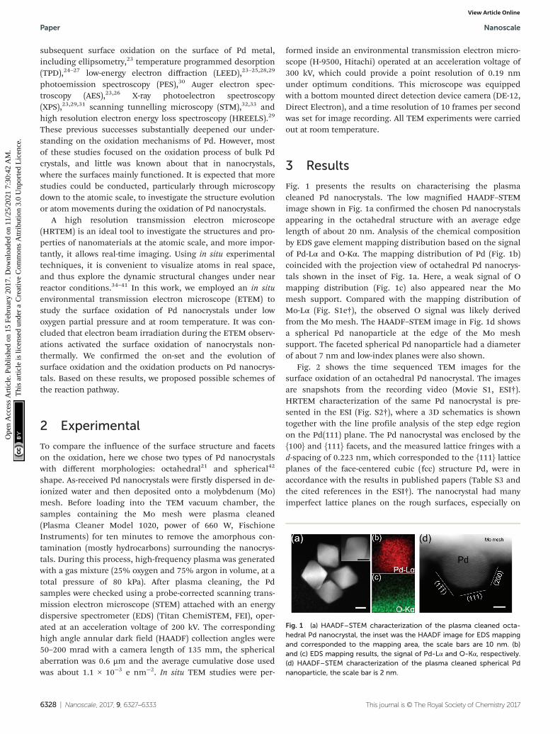
Fig. 1 presents the results on characterising the plasmacleaned Pd nanocrystals. The low magnified HAADF–STEMimage shown in Fig. 1a confirmed the chosen Pd nanocrystalsappearing in the octahedral structure with an average edgelength of about 20 nm. Analysis of the chemical compositionby EDS gave element mapping distribution based on the signalof Pd-Lα and O-Kα. The mapping distribution of Pd (Fig. 1b)coincided with the projection view of octahedral Pd nanocrys-tals shown in the inset of Fig. 1a. Here, a weak signal of Omapping distribution (Fig. 1c) also appeared near the Momesh support. Compared with the mapping distribution ofMo-Lα (Fig. S1e†), the observed O signal was likely derivedfrom the Mo mesh. The HAADF–STEM image in Fig. 1d showsa spherical Pd nanoparticle at the edge of the Mo meshsupport. The faceted spherical Pd nanoparticle had a diameterof about 7 nm and low-index planes were also shown.
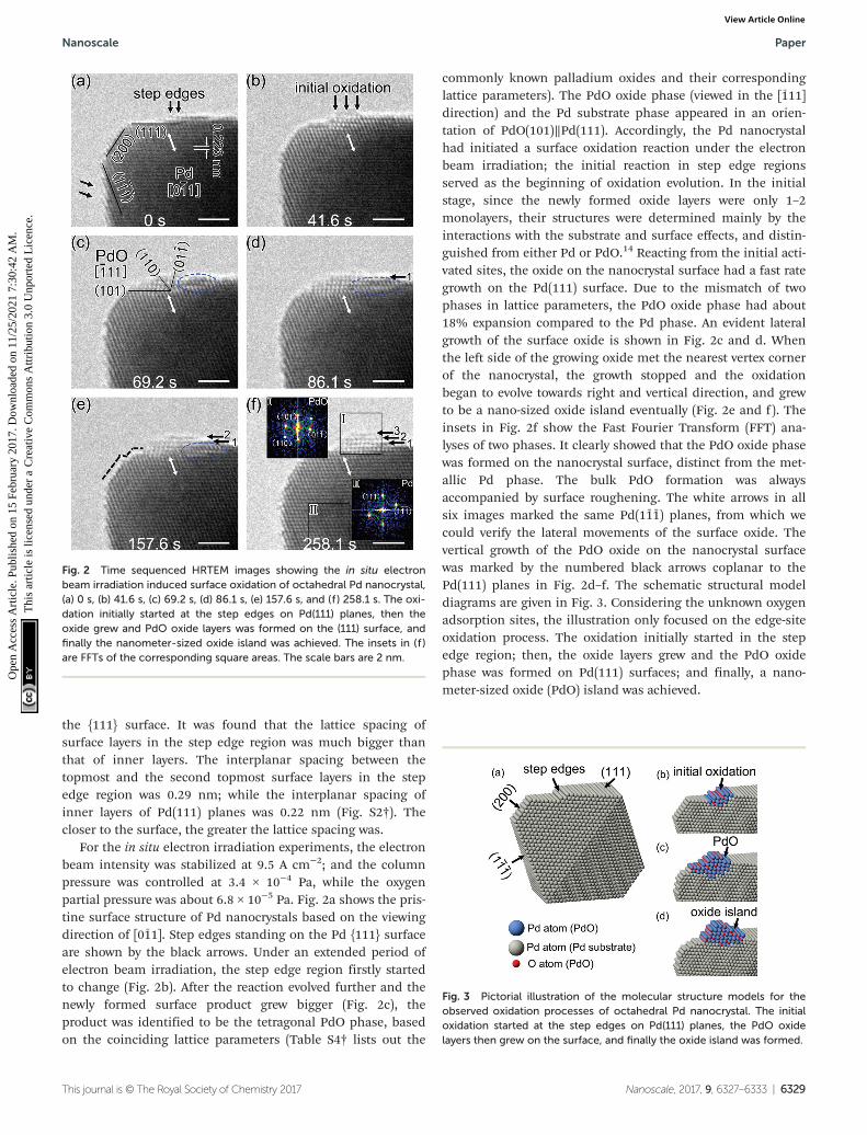
Fig. 2 shows the time sequenced TEM images for thesurface oxidation of an octahedral Pd nanocrystal. The imagesare snapshots from the recording video (Movie S1, ESI†).HRTEM characterization of the same Pd nanocrystal is pre-sented in the ESI (Fig. S2†), where a 3D schematics is showntogether with the line profile analysis of the step edge regionon the Pd(111) plane. The Pd nanocrystal was enclosed by the{100} and {111} facets, and the measured lattice fringes with ad-spacing of 0.223 nm, which corresponded to the {111} latticeplanes of the face-centered cubic (fcc) structure Pd, were inaccordance with the results in published papers (Table S3 andthe cited references in the ESI†). The nanocrystal had manyimperfect lattice planes on the rough surfaces, especially on
Fig. 1 (a) HAADF–STEM characterization of the plasma cleaned octa-hedral Pd nanocrystal, the inset was the HAADF image for EDS mappingand corresponded to the mapping area, the scale bars are 10 nm. (b)and (c) EDS mapping results, the signal of Pd-Lα and O-Kα, respectively.(d) HAADF–STEM characterization of the plasma cleaned spherical Pdnanoparticle, the scale bar is 2 nm.
Paper Nanoscale
6328 | Nanoscale, 2017, 9, 6327–6333 This journal is © The Royal Society of Chemistry 2017
Ope
n A
cces
s A
rtic
le. P
ublis
hed
on 1
5 Fe
brua
ry 2
017.
Dow
nloa
ded
on 1
1/25
/202
1 7:
30:4
2 A
M.
Thi
s ar
ticle
is li
cens
ed u
nder
a C
reat
ive
Com
mon
s A
ttrib
utio
n 3.
0 U
npor
ted
Lic
ence
.View Article Online
the {111} surface. It was found that the lattice spacing ofsurface layers in the step edge region was much bigger thanthat of inner layers. The interplanar spacing between thetopmost and the second topmost surface layers in the stepedge region was 0.29 nm; while the interplanar spacing ofinner layers of Pd(111) planes was 0.22 nm (Fig. S2†). Thecloser to the surface, the greater the lattice spacing was.
For the in situ electron irradiation experiments, the electronbeam intensity was stabilized at 9.5 A cm−2; and the columnpressure was controlled at 3.4 × 10⁻⁴ Pa, while the oxygenpartial pressure was about 6.8 × 10⁻⁵ Pa. Fig. 2a shows the pris-tine surface structure of Pd nanocrystals based on the viewingdirection of [01̄1]. Step edges standing on the Pd {111} surfaceare shown by the black arrows. Under an extended period ofelectron beam irradiation, the step edge region firstly startedto change (Fig. 2b). After the reaction evolved further and thenewly formed surface product grew bigger (Fig. 2c), theproduct was identified to be the tetragonal PdO phase, basedon the coinciding lattice parameters (Table S4† lists out the
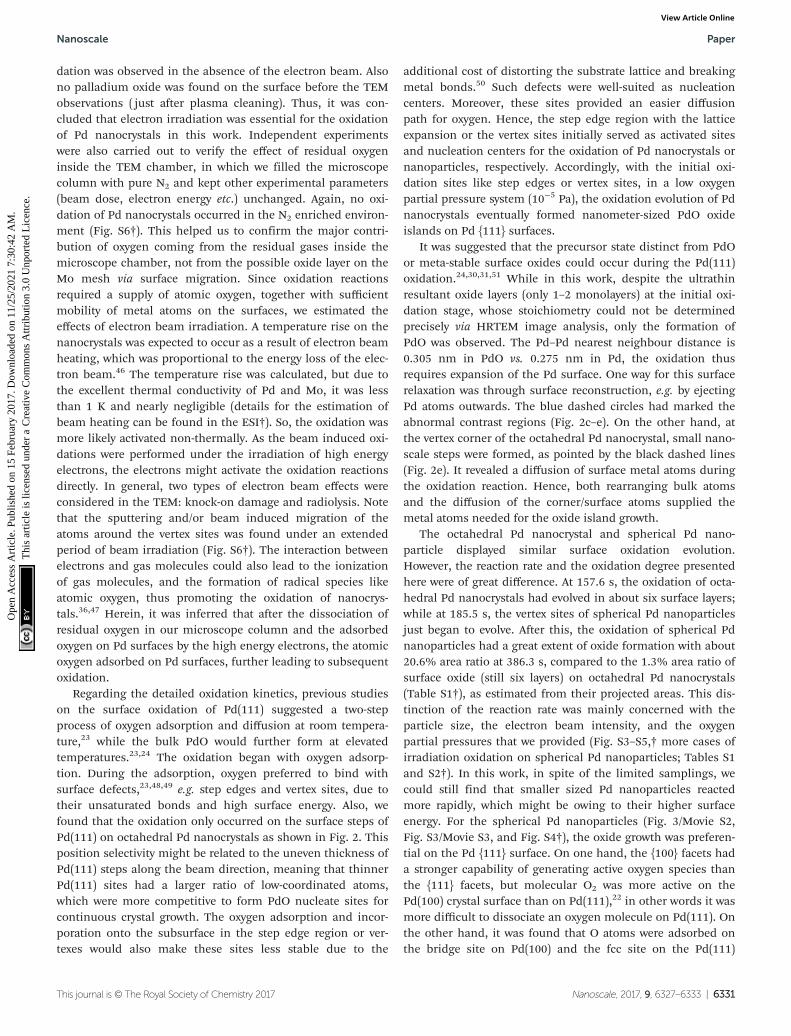
commonly known palladium oxides and their correspondinglattice parameters). The PdO oxide phase (viewed in the [1̄11]direction) and the Pd substrate phase appeared in an orien-tation of PdO(101)∥Pd(111). Accordingly, the Pd nanocrystalhad initiated a surface oxidation reaction under the electronbeam irradiation; the initial reaction in step edge regionsserved as the beginning of oxidation evolution. In the initialstage, since the newly formed oxide layers were only 1–2monolayers, their structures were determined mainly by theinteractions with the substrate and surface effects, and distin-guished from either Pd or PdO.14 Reacting from the initial acti-vated sites, the oxide on the nanocrystal surface had a fast rategrowth on the Pd(111) surface. Due to the mismatch of twophases in lattice parameters, the PdO oxide phase had about18% expansion compared to the Pd phase. An evident lateralgrowth of the surface oxide is shown in Fig. 2c and d. Whenthe left side of the growing oxide met the nearest vertex cornerof the nanocrystal, the growth stopped and the oxidationbegan to evolve towards right and vertical direction, and grewto be a nano-sized oxide island eventually (Fig. 2e and f). Theinsets in Fig. 2f show the Fast Fourier Transform (FFT) ana-lyses of two phases. It clearly showed that the PdO oxide phasewas formed on the nanocrystal surface, distinct from the met-allic Pd phase. The bulk PdO formation was alwaysaccompanied by surface roughening. The white arrows in allsix images marked the same Pd(11̄1̄) planes, from which wecould verify the lateral movements of the surface oxide. Thevertical growth of the PdO oxide on the nanocrystal surfacewas marked by the numbered black arrows coplanar to thePd(111) planes in Fig. 2d–f. The schematic structural modeldiagrams are given in Fig. 3. Considering the unknown oxygenadsorption sites, the illustration only focused on the edge-siteoxidation process. The oxidation initially started in the stepedge region; then, the oxide layers grew and the PdO oxidephase was formed on Pd(111) surfaces; and finally, a nano-meter-sized oxide (PdO) island was achieved.
Fig. 2 Time sequenced HRTEM images showing the in situ electronbeam irradiation induced surface oxidation of octahedral Pd nanocrystal,(a) 0 s, (b) 41.6 s, (c) 69.2 s, (d) 86.1 s, (e) 157.6 s, and (f ) 258.1 s. The oxi-dation initially started at the step edges on Pd(111) planes, then theoxide grew and PdO oxide layers was formed on the (111) surface, andfinally the nanometer-sized oxide island was achieved. The insets in (f )are FFTs of the corresponding square areas. The scale bars are 2 nm.
Fig. 3 Pictorial illustration of the molecular structure models for theobserved oxidation processes of octahedral Pd nanocrystal. The initialoxidation started at the step edges on Pd(111) planes, the PdO oxidelayers then grew on the surface, and finally the oxide island was formed.
Nanoscale Paper
This journal is © The Royal Society of Chemistry 2017 Nanoscale, 2017, 9, 6327–6333 | 6329
Ope
n A
cces
s A
rtic
le. P
ublis
hed
on 1
5 Fe
brua
ry 2
017.
Dow
nloa
ded
on 1
1/25
/202
1 7:
30:4
2 A
M.
Thi
s ar
ticle
is li
cens
ed u
nder
a C
reat
ive
Com
mon
s A
ttrib
utio
n 3.
0 U
npor
ted
Lic
ence
.View Article Online

Spherical Pd nanoparticles were also employed in ourinvestigations to show that the beam induced surface oxi-dation of octahedral Pd nanocrystals was not an exceptionalcase. Sequential TEM images showing the structure evolutionof a spherical Pd nanoparticle, which was also induced by elec-tron irradiation, are presented in Fig. 4. TEM experiments werecarried out using the same procedure as that of the octahedralPd nanocrystals. Herein, the electron beam intensity was con-trolled at 3.3 A cm−2 by considering reaction rate control for amuch smaller-sized Pd nanoparticle, and the column pressurewas stabilized at 9.5 × 10⁻⁴ Pa, with an oxygen partial pressureof about 1.9 × 10⁻⁴ Pa. Fig. 4a shows the Mo mesh supportedspherical Pd nanoparticle with a size of about 7 nm in dia-meter. It had a faceted structure. A few low-index planes wereshown based on the viewing direction of [011̄]. The measuredlattice fringes with a d-spacing of 0.224 nm corresponded tothe Pd {111} planes. The initial reaction started from the vertex
sites of Pd(111) and Pd(11̄1̄) planes, highlighted by blackarrows (Fig. 4b). With further irradiation, the reaction evolu-tion spread from the vertex sites to the Pd(11̄1̄) surface(Fig. 4c). But this spreading stopped at the other side ofPd(11̄1̄) planes, marked by black triangles (Fig. 4c and d). Inthe following stage, the resultant began a three-dimensionalgrowth on the Pd(11̄1̄) surface (Fig. 4e). As shown in Fig. 4f,the reaction resultant was also confirmed to be PdO based onthe interplanar spacing measurements. The d-spacings of0.263 nm corresponded to the (101) and (101̄) planes of a tetra-gonal PdO, in the viewing direction of [01̄0]; and the on-surface PdO oxide was found to be PdO(101)∥Pd(11̄1̄).Schematic diagrams of the observed oxidation for the sphericalPd nanoparticles are drawn and shown in Fig. 5. The oxidationof faceted Pd nanoparticles started at the vertex sites and PdOoxide was formed on the Pd(11̄1̄) surface eventually.
4 Discussions
We firstly discussed the effects of plasma cleaning for theadsorption and subsequent oxidation of Pd nanocrystals. Theintroduced oxygen would be plasma excited to form differenttypes of radical species, such as O2+, O2−, O2*, O3, O, O
+, O−,O*, etc., and some of them could further interact with thesurface of nanocrystals, physically and/or chemically.43 Forinstance, Kim et al. confirmed the formation of an oxygen-enriched surface on the surface of Pt.44 As per our studies, theoxygen adsorption and atom/ion implantation might occurduring the plasma treatment and cause weak oxidation on theoutermost layers. For the octahedral Pd nanocrystal, we hadobserved an expansion of about 32% in the outermost layer inthe step edge region standing on the Pd(111) surface (Fig. S2†)which was likely exacerbated by the plasma bombardment,and/or the knock-on damage of energetic electrons duringTEM imaging. Nevertheless, the adsorption of oxygen onto thePd surface was reported to be a spontaneous process.22,45 Dueto the limitation of our TEM, we were not able to capture theadsorbed oxygen molecules on the surface of Pd nanocrystals.
Back to the oxidation evolution, the energetic electronbeam and the oxidation mechanism were much relevant. ForPd nanocrystals loaded on the same Mo grid, no obvious oxi-
Fig. 4 Sequential HRTEM images showing the in situ oxidation of afaceted Pd nanoparticle, (a) 0 s, (b) 185.5 s, (c) 206.3 s, (d) 227.4 s, (e)351.9 s, and (f ) 386.3 s. The oxidation started at the vertex of Pd(111) andPd(11̄1̄) planes, then evolved towards the Pd(11̄1̄) surface, but stopped atthe other side of Pd(11̄1̄) planes. Continuously, the oxide began a three-dimensional growth on the Pd(11̄1̄) surface and the PdO oxide wasformed finally. The scale bars are 2 nm.
Fig. 5 Schematic diagrams for the observed oxidation of a spherical Pdnanoparticle. The oxidation started from the vertex sites of Pd(111) andPd(11̄1̄) planes, and the PdO oxide was formed on the Pd(11̄1̄) surfaceeventually.
Paper Nanoscale
6330 | Nanoscale, 2017, 9, 6327–6333 This journal is © The Royal Society of Chemistry 2017
Ope
n A
cces
s A
rtic
le. P
ublis
hed
on 1
5 Fe
brua
ry 2
017.
Dow
nloa
ded
on 1
1/25
/202
1 7:
30:4
2 A
M.
Thi
s ar
ticle
is li
cens
ed u
nder
a C
reat
ive
Com
mon
s A
ttrib
utio
n 3.
0 U
npor
ted
Lic
ence
.View Article Online
dation was observed in the absence of the electron beam. Alsono palladium oxide was found on the surface before the TEMobservations ( just after plasma cleaning). Thus, it was con-cluded that electron irradiation was essential for the oxidationof Pd nanocrystals in this work. Independent experimentswere also carried out to verify the effect of residual oxygeninside the TEM chamber, in which we filled the microscopecolumn with pure N2 and kept other experimental parameters(beam dose, electron energy etc.) unchanged. Again, no oxi-dation of Pd nanocrystals occurred in the N2 enriched environ-ment (Fig. S6†). This helped us to confirm the major contri-bution of oxygen coming from the residual gases inside themicroscope chamber, not from the possible oxide layer on theMo mesh via surface migration. Since oxidation reactionsrequired a supply of atomic oxygen, together with sufficientmobility of metal atoms on the surfaces, we estimated theeffects of electron beam irradiation. A temperature rise on thenanocrystals was expected to occur as a result of electron beamheating, which was proportional to the energy loss of the elec-tron beam.46 The temperature rise was calculated, but due tothe excellent thermal conductivity of Pd and Mo, it was lessthan 1 K and nearly negligible (details for the estimation ofbeam heating can be found in the ESI†). So, the oxidation wasmore likely activated non-thermally. As the beam induced oxi-dations were performed under the irradiation of high energyelectrons, the electrons might activate the oxidation reactionsdirectly. In general, two types of electron beam effects wereconsidered in the TEM: knock-on damage and radiolysis. Notethat the sputtering and/or beam induced migration of theatoms around the vertex sites was found under an extendedperiod of beam irradiation (Fig. S6†). The interaction betweenelectrons and gas molecules could also lead to the ionizationof gas molecules, and the formation of radical species likeatomic oxygen, thus promoting the oxidation of nanocrys-tals.36,47 Herein, it was inferred that after the dissociation ofresidual oxygen in our microscope column and the adsorbedoxygen on Pd surfaces by the high energy electrons, the atomicoxygen adsorbed on Pd surfaces, further leading to subsequentoxidation.
Regarding the detailed oxidation kinetics, previous studieson the surface oxidation of Pd(111) suggested a two-stepprocess of oxygen adsorption and diffusion at room tempera-ture,23 while the bulk PdO would further form at elevatedtemperatures.23,24 The oxidation began with oxygen adsorp-tion. During the adsorption, oxygen preferred to bind withsurface defects,23,48,49 e.g. step edges and vertex sites, due totheir unsaturated bonds and high surface energy. Also, wefound that the oxidation only occurred on the surface steps ofPd(111) on octahedral Pd nanocrystals as shown in Fig. 2. Thisposition selectivity might be related to the uneven thickness ofPd(111) steps along the beam direction, meaning that thinnerPd(111) sites had a larger ratio of low-coordinated atoms,which were more competitive to form PdO nucleate sites forcontinuous crystal growth. The oxygen adsorption and incor-poration onto the subsurface in the step edge region or ver-texes would also make these sites less stable due to the
additional cost of distorting the substrate lattice and breakingmetal bonds.50 Such defects were well-suited as nucleationcenters. Moreover, these sites provided an easier diffusionpath for oxygen. Hence, the step edge region with the latticeexpansion or the vertex sites initially served as activated sitesand nucleation centers for the oxidation of Pd nanocrystals ornanoparticles, respectively. Accordingly, with the initial oxi-dation sites like step edges or vertex sites, in a low oxygenpartial pressure system (10−5 Pa), the oxidation evolution of Pdnanocrystals eventually formed nanometer-sized PdO oxideislands on Pd {111} surfaces.
It was suggested that the precursor state distinct from PdOor meta-stable surface oxides could occur during the Pd(111)oxidation.24,30,31,51 While in this work, despite the ultrathinresultant oxide layers (only 1–2 monolayers) at the initial oxi-dation stage, whose stoichiometry could not be determinedprecisely via HRTEM image analysis, only the formation ofPdO was observed. The Pd–Pd nearest neighbour distance is0.305 nm in PdO vs. 0.275 nm in Pd, the oxidation thusrequires expansion of the Pd surface. One way for this surfacerelaxation was through surface reconstruction, e.g. by ejectingPd atoms outwards. The blue dashed circles had marked theabnormal contrast regions (Fig. 2c–e). On the other hand, atthe vertex corner of the octahedral Pd nanocrystal, small nano-scale steps were formed, as pointed by the black dashed lines(Fig. 2e). It revealed a diffusion of surface metal atoms duringthe oxidation reaction. Hence, both rearranging bulk atomsand the diffusion of the corner/surface atoms supplied themetal atoms needed for the oxide island growth.
The octahedral Pd nanocrystal and spherical Pd nano-particle displayed similar surface oxidation evolution.However, the reaction rate and the oxidation degree presentedhere were of great difference. At 157.6 s, the oxidation of octa-hedral Pd nanocrystals had evolved in about six surface layers;while at 185.5 s, the vertex sites of spherical Pd nanoparticlesjust began to evolve. After this, the oxidation of spherical Pdnanoparticles had a great extent of oxide formation with about20.6% area ratio at 386.3 s, compared to the 1.3% area ratio ofsurface oxide (still six layers) on octahedral Pd nanocrystals(Table S1†), as estimated from their projected areas. This dis-tinction of the reaction rate was mainly concerned with theparticle size, the electron beam intensity, and the oxygenpartial pressures that we provided (Fig. S3–S5,† more cases ofirradiation oxidation on spherical Pd nanoparticles; Tables S1and S2†). In this work, in spite of the limited samplings, wecould still find that smaller sized Pd nanoparticles reactedmore rapidly, which might be owing to their higher surfaceenergy. For the spherical Pd nanoparticles (Fig. 3/Movie S2,Fig. S3/Movie S3, and Fig. S4†), the oxide growth was preferen-tial on the Pd {111} surface. On one hand, the {100} facets hada stronger capability of generating active oxygen species thanthe {111} facets, but molecular O2 was more active on thePd(100) crystal surface than on Pd(111),22 in other words it wasmore difficult to dissociate an oxygen molecule on Pd(111). Onthe other hand, it was found that O atoms were adsorbed onthe bridge site on Pd(100) and the fcc site on the Pd(111)
Nanoscale Paper
This journal is © The Royal Society of Chemistry 2017 Nanoscale, 2017, 9, 6327–6333 | 6331
Ope
n A
cces
s A
rtic
le. P
ublis
hed
on 1
5 Fe
brua
ry 2
017.
Dow
nloa
ded
on 1
1/25
/202
1 7:
30:4
2 A
M.
Thi
s ar
ticle
is li
cens
ed u
nder
a C
reat
ive
Com
mon
s A
ttrib
utio
n 3.
0 U
npor
ted
Lic
ence
.View Article Online

surface, and O atoms had much higher adsorption energies onPd(100) (−4.70 eV) than on the Pd(111) (−4.49 eV) surface.52
The irradiation of high energy electrons not only decomposedoxygen molecules into atomic oxygen promoting the oxidationas mentioned above, but could also desorb oxygen from themetal/metal oxide surfaces due to the knock-on effect andsurface sputtering. The balance of the competing effectsdepended on the partial pressure of gases, the electron currentdensity and the orientation of surfaces with respect to the elec-tron beam.36 Herein, the {111} surface was likely to havehigher oxygen coverage under the provided experimental con-ditions, thus a preferential oxide growth on Pd {111} surfaceswas observed on spherical Pd nanoparticles. It would be inter-esting to control these factors, like oxygen pressure, electronbeam intensity and temperature, to identify their contri-butions. Although here we used an electron beam to decom-pose O2 and activated the oxidation, the ion diffusion and oxi-dation features, like the initial reaction at step edges or vertexsites, and the crystallography preference, could offer guidancefor understanding the oxidation mechanisms of metals at thenanoscale, especially at low oxygen pressure and low tempera-ture involved oxidation reactions.
5 Conclusions
In summary, we have presented an in situ study on the surfaceoxidation behaviour of Pd nanocrystals induced by electronbeam irradiation using two types of Pd nanocrystals, as octa-hedral and spherical structures. Valuable insights into thesurface oxidation process and surface diffusion are obtained.The observations at the atomic scale showed that the oxidationpreferred to launch reactions at the active sites, like the stepedges or the vertex sites. The faceted spherical Pd nano-particles showed a crystallography preference for the surfaceoxidation, which was on the Pd {111} surface. Both Pd nano-crystals were oxidized and formed nanometer-sized PdO oxideislands. The electron beam in the microscope had promotedthe oxidation on Pd nanocrystals. The oxidation layer thick-ness and/or the island size depend on the oxygen partialpressure in the column, the irradiation time and the e-beamdose on the samples.
Acknowledgements
This work was financially supported by the National NaturalScience Foundation of China (Grant No. 11227403, 51472215,51222202 and 91545113), and the Cyrus Tang Center for SensorMaterials and Applications. The work in the UK was supportedby Engineering and Physical Sciences Research Council (GrantNo. EP/G070326/1). Z. Y. Li thanks the Qiushi Foundation for avisiting Chair Professorship in ZJU. The collaboration betweenUK and CN side was supported by the 111 project under grantNo. B16042. This work made use of the resources of the Centerof Electron Microscopy of Zhejiang University.
Notes and references
1 K. Zhou and Y. Li, Angew. Chem., Int. Ed., 2012, 51, 602–613.
2 J. Park, J. Joo, S. G. Kwon, Y. Jang and T. Hyeon, Angew.Chem., Int. Ed., 2007, 46, 4630–4660.
3 Y. Zhou, Z. Wang and C. Liu, Catal. Sci. Technol., 2015, 5,69–81.
4 W. Zang, G. Li, L. Wang and X. Zhang, Catal. Sci. Technol.,2015, 5, 2532–2553.
5 Y. Han, Z. Y. He, S. L. Wang, W. Li and J. L. Zhang, Catal.Sci. Technol., 2015, 5, 2630–2639.
6 B. L. Hendriksen and J. W. Frenken, Phys. Rev. Lett., 2002,89, 046101.
7 H. Over, Y. D. Kim, A. P. Seitsonen, S. Wendt, E. Lundgren,M. Schmid, P. Varga, A. Morgante and G. Ertl, Science,2000, 287, 1474–1476.
8 D. W. Goodman, C. H. F. Peden and M. S. Chen, Surf. Sci.,2007, 601, L124–L126.
9 M. Lyubovsky and L. Pfefferle, Catal. Today, 1999, 47, 29–44.
10 J. G. McCarty, Catal. Today, 1995, 26, 283–293.11 M. Lyubovsky, L. Pfefferle, A. Datye, J. Bravo and T. Nelson,
J. Catal., 1999, 187, 275–284.12 M. Crespo-Quesada, A. Yarulin, M. Jin, Y. Xia and L. Kiwi-
Minsker, J. Am. Chem. Soc., 2011, 133, 12787–12794.13 E. Antolini, Energy Environ. Sci., 2009, 2, 915–931.14 D. Ciuparu, M. R. Lyubovsky, E. Altman, L. D. Pfefferle and
A. Datye, Catal. Rev.: Sci. Eng., 2002, 44, 593–649.15 M. Jin, H. Liu, H. Zhang, Z. Xie, J. Liu and Y. Xia, Nano
Res., 2010, 4, 83–91.16 Y. Piao, Y. Jang, M. Shokouhimehr, I. S. Lee and T. Hyeon,
Small, 2007, 3, 255–260.17 X. Zhang, H. Yin, J. Wang, L. Chang, Y. Gao, W. Liu and
Z. Tang, Nanoscale, 2013, 5, 8392–8397.18 S. Cheong, J. D. Watt and R. D. Tilley, Nanoscale, 2010, 2,
2045–2053.19 R. Wang, H. He, L. C. Liu, H. X. Dai and Z. Zhao, Catal. Sci.
Technol., 2012, 2, 575–580.20 B. L. Hendriksen, M. D. Ackermann, R. van Rijn, D. Stoltz,
I. Popa, O. Balmes, A. Resta, D. Wermeille, R. Felici,S. Ferrer and J. W. Frenken, Nat. Chem., 2010, 2, 730–734.
21 M. S. Jin, H. Zhang, Z. X. Xie and Y. N. Xia, Energy Environ.Sci., 2012, 5, 6352–6357.
22 R. Long, K. Mao, X. Ye, W. Yan, Y. Huang, J. Wang, Y. Fu,X. Wang, X. Wu, Y. Xie and Y. Xiong, J. Am. Chem. Soc.,2013, 135, 3200–3207.
23 E. H. Voogt, A. J. M. Mens, O. L. J. Gijzeman andJ. W. Geus, Surf. Sci., 1997, 373, 210–220.
24 G. Zheng and E. I. Altman, Surf. Sci., 2000, 462, 151–168.25 G. Zheng and E. I. Altman, Surf. Sci., 2002, 504, 253–270.26 J. Han, D. Y. Zemlyanov and F. H. Ribeiro, Surf. Sci., 2006,
600, 2752–2761.27 H. H. Kan, R. B. Shumbera and J. F. Weaver, Surf. Sci.,
2008, 602, 1337–1346.28 T. W. Orent and S. D. Bader, Surf. Sci., 1982, 115, 323–334.
Paper Nanoscale
6332 | Nanoscale, 2017, 9, 6327–6333 This journal is © The Royal Society of Chemistry 2017
Ope
n A
cces
s A
rtic
le. P
ublis
hed
on 1
5 Fe
brua
ry 2
017.
Dow
nloa
ded
on 1
1/25
/202
1 7:
30:4
2 A
M.
Thi
s ar
ticle
is li
cens
ed u
nder
a C
reat
ive
Com
mon
s A
ttrib
utio
n 3.
0 U
npor
ted
Lic
ence
.View Article Online

29 F. P. Leisenberger, G. Koller, M. Sock, S. Surnev,M. G. Ramsey, F. P. Netzer, B. Klotzer and K. Hayek, Surf.Sci., 2000, 445, 380–393.
30 G. Ketteler, D. F. Ogletree, H. Bluhm, H. Liu,E. L. Hebenstreit and M. Salmeron, J. Am. Chem. Soc., 2005,127, 18269–18273.
31 H. Gabasch, W. Unterberger, K. Hayek, B. Klötzer,E. Kleimenov, D. Teschner, S. Zafeiratos, M. Hävecker,A. Knop-Gericke, R. Schlögl, J. Han, F. H. Ribeiro,B. Aszalos-Kiss, T. Curtin and D. Zemlyanov, Surf. Sci.,2006, 600, 2980–2989.
32 M. K. Rose, A. Borg, J. C. Dunphy, T. Mitsui, D. F. Ogletreeand M. Salmeron, Surf. Sci., 2003, 547, 162–170.
33 M. K. Rose, A. Borg, J. C. Dunphy, T. Mitsui, D. F. Ogletreeand A. Salmeron, Surf. Sci., 2004, 561, 69–78.
34 H. Yoshida, Y. Kuwauchi, J. R. Jinschek, K. Sun, S. Tanaka,M. Kohyama, S. Shimada, M. Haruta and S. Takeda,Science, 2012, 335, 317–319.
35 T. Fujita, T. Tokunaga, L. Zhang, D. Li, L. Chen, S. Arai,Y. Yamamoto, A. Hirata, N. Tanaka, Y. Ding and M. Chen,Nano Lett., 2014, 14, 1172–1177.
36 H. Yoshida, H. Omote and S. Takeda, Nanoscale, 2014, 6,13113–13118.
37 X. Huang, T. Jones, H. Fan and M.-G. Willinger, Adv. Mater.Interfaces, 2016, 3, 1600751.
38 Y. Jiang, G. Zhu, F. Lin, H. Zhang, C. Jin, J. Yuan, D. Yangand Z. Zhang, Nano Lett., 2014, 14, 3761–3765.
39 W. Yuan, Y. Wang, H. Li, H. Wu, Z. Zhang, A. Selloni andC. Sun, Nano Lett., 2016, 16, 132–137.
40 W. Liu, K. Sun and R. Wang, Nanoscale, 2013, 5, 5067–5072.
41 X. Xiang, J. Nie, K. Sun, L. Zhang, W. Liu, J. Schwank,S. Wang, M. Zhong, F. Gao and X. Zu, Nanoscale, 2014, 6,12898–12904.
42 N. Zheng, J. Fan and G. D. Stucky, J. Am. Chem. Soc., 2006,128, 6550–6551.
43 M. Mozetic, U. Cvelbar, M. K. Sunkara and S. Vaddiraju,Adv. Mater., 2005, 17, 2138–2142.
44 S. Y. Kim, K. Hong, K. Kim, H. K. Yu, W.-K. Kim andJ.-L. Lee, J. Appl. Phys., 2008, 103, 076101.
45 Z. X. Wang, X. F. Jia and R. Wang, J. Chem. Phys. A, 2004,108, 5424–5430.
46 R. F. Egerton, P. Li and M. Malac, Micron, 2004, 35, 399–409.
47 J. B. Wagner, F. Cavalca, C. D. Damsgaard, L. D. Duchsteinand T. W. Hansen, Micron, 2012, 43, 1169–1175.
48 M. Okada, L. Vattuone, M. Rocca and Y. Teraoka, J. Chem.Phys., 2012, 136, 094704.
49 L. Li, L. Luo, J. Ciston, W. A. Saidi, E. A. Stach, J. C. Yangand G. Zhou, Phys. Rev. Lett., 2014, 113, 136104.
50 M. Todorova, W. X. Li, M. V. Ganduglia-Pirovano,C. Stampfl, K. Reuter and M. Scheffler, Phys. Rev. Lett.,2002, 89, 096103.
51 J. Klikovits, E. Napetschnig, M. Schmid, N. Seriani,O. Dubay, G. Kresse and P. Varga, Phys. Rev. B: Condens.Matter, 2007, 76, 045405.
52 C. Q. Lv, K. C. Ling and G. C. Wang, J. Chem. Phys., 2009,131, 144704.
Nanoscale Paper
This journal is © The Royal Society of Chemistry 2017 Nanoscale, 2017, 9, 6327–6333 | 6333
Ope
n A
cces
s A
rtic
le. P
ublis
hed
on 1
5 Fe
brua
ry 2
017.
Dow
nloa
ded
on 1
1/25
/202
1 7:
30:4
2 A
M.
Thi
s ar
ticle
is li
cens
ed u
nder
a C
reat
ive
Com
mon
s A
ttrib
utio
n 3.
0 U
npor
ted
Lic
ence
.View Article Online