an automatic antenna matching method for monostatic fmcw...
TRANSCRIPT

An automatic antenna matching method for monostatic FMCW
radars
Professor: Prof. Dr.-Ing. Klaus SolbachSupervisor: Dipl. -Ing. Michael ThielStudent: Yan Shen

Outline
• Introduction • System Development and Design• Impedance Tuner Design• Test Results• Controller Algorithm• Conclusions and Further Work

IntroductionHardware Realization of the FMCW Monostatic Radar
)]2cos()[cos(2
21)]cos()[cos(21)]cos(2)][cos(1[ 1212121 ωωωωωωωωω +Δ+Δ=++−==×AAAAAARXTX
RXRXnTXRXRXnTXRX ××+×=×+× )(
If RX and TX are not well decoupled:DC offset
Reduced performance of the mixer due to changed DC operation.
fd Δ≈ /1

if Zimage(V1,V2) = Zantenna, RX and TX are well decoupled.
Impedance tuner
Decoupling Diplexers
Antenna impedance changes
Rat-race coupler
Temperatures, radiation environments

• Rat-race Coupler• Wilkinson Power Divider• Gilbert Cell Mixer• Patch Antenna• System Modelling and Development
System Design and Development

Rat-race CouplerADS layout Schematic VS Momentum
P1
P2 P3
P4

Wilkinson Power DividerADS layout
P1
P2
P3
Schematic VS Momentum

Gilbert Cell Mixer
y1
y2
IF output
LO input
RF input
V_DCSRC4Vdc=5.6 V
RR7R=1200 Ohm
RR9R=0.6 kOhm
RR10R=0.6 kOhm
CC5C=1 pF
OpAmpAMP1
VCC=5 VVEE=-5 VZero1=Pole1=BW=500 MHzVOS=200 uVIOS=0.2 uASlewRate=5e+8CCom=1 pFRCom=1 MOhmCDiff=1 pFRDiff=15 kOhmRout=100 OhmCMR=75 dBGain=60 dB
PortP3Num=3
RR8R=1200 Ohm
PortP2Num=2
V_DCSRC2Vdc=1.9 V
RR1R=10 Ohm
I_DCSRC3Idc=0.06 mA
V_DCSRC1Vdc=2.9 V
RR2R=10 Ohm
npnH3shp4Q5Icmax=8 mA
rpndR5
Imax=0.24 mAl=5.72 umw=0.48 umR=3 kOhm
npnH3shp4Q1Icmax=8 mA
rpndR4
Imax=0.24 mAl=5.72 umw=0.48 umR=3 kOhm
PortP1Num=1
rpndR6
Imax=0.24 mAl=5.72 umw=0.48 umR=3 kOhm
npnH3shp8Q7Icmax=16 mA
rpndR3
Imax=0.24 mAl=5.72 umw=0.48 umR=3 kOhm
cmimC4
l=54.71 umw=54.71 umc=3 pF
cmimC3
l=54.71 umw=54.71 umc=3 pF
cmimC2
l=54.71 umw=54.71 umc=3 pF
cmimC1
l=54.71 umw=54.71 umc=3 pF
npnH3shp4Q6Icmax=8 mA
npnH3shp4Q4Icmax=8 mA
npnH3shp4Q2Icmax=8 mA
npnH3shp4Q3Icmax=8 mA
Mixer schematic Power level test

Single inset-fed patch antenna
Twin inset-fed patch antenna
Quad inset-fed patch antenna
larger bandwidth
Patch Antenna
largest bandwidth

System Modelling
Case 1 Case 2 IF_gain=20log(1.015/0.066)=24dB!
Case 1:R_image=50 Ohm, E_image=0Case 2:R_image=25 Ohm, E_image=80

@10.00G
-21.10dBm
1.34dBm
@10.01G
-26.23dBm
-40.97dBm
DC�0.486V10 MHz�1.613V
System Matching

Reflection Tuner
The traditional transmission tuner: Additional induced losses on thefeed line due to multiple reflections and losses in the ATU itself:
The reflection tuner:Losses on the tuner has no influence to the system.
Tuner Design
Transmission Tuner

Principle of our tuner
C1: 0~90°tune the phase
Simulation result:
TLINTL1
F=10 GHzE=C1Z=50.0 Ohm
RR1R=RX Ohm
TermTerm1
Z=50 OhmNum=1
RX: 33.3~75 Ohmtune the amplitude
Tuner schematic:
Phase shifterVariable resistor

FET as Voltage-controlled Resistorsnonlinear Triquint MGF1402 package.
Ugs:-0.5913 ~ -0.5101 V
MGF1402
Rds~Ugs

Phase Shifter Design
Variable reactance reflection phase shifter
Lange coupler
Branch-line coupler
90°hybrid coupler:

Phase shifter schematic:Branch-line coupler and Silicon tunning Varactor SMV 2019-108
Phase shift: 218°
Simulation result:P1 P2
Udiode: 0~20 V

Tuner Schematic:
Udiode: 0~20V
Ufet: -0.6~0V
Simulation result: PCB:

PCB of the Final Radar System

Test ResultsRat-race coupler Power divider
PCB VS Momentum
Branch-line coupler
NWA

Antenna Tuner
Phase shift is not enough;FET works good.
Two ways to improve
Too high series inductance
PCB VS Momentum

(a)
(b)
(c)

Controller SystemReal control system
),( UdiodeUfetfUdc =
Original data set Interpolation
in Matlab
Udc=Interp(Udiode, Ufet)
Minisearch function in Matlab
Starting points
Udcmin
Udiode, Ufet
HP 4142BModularDC
Source
SMU0
SMU1
Udiode
Ufet
Radar system
Udc
OptimizerDAQInstrument
Control algorithm
Simulated control system
Optimizer ADS model
Aim: Minimize Udc

Three dimentional plotted graph Original data set, Column 1 is Udiode and Column 2 is Ufet. Column 3 is Udc.

1. [x, fval, history, DC] = func2 ([1, 0]) Result: x = 4.7380 -0.0219
fval = 2.5215e-005
2. [x,fval,history,DC]=func2([3,-0.4])Result: x = 4.9778 -0.2191
fval = 5.0413e-010
Examples
3. [x,fval,history,DC]=func2([2,-0.5])Result: x = 2.0001 -0.7000
fval = 2.0723

ConclusionsThis master thesis developed a dynamic method to minimize the DC offset at the output of the mixer. A demonstrator was built on an RF grade circuit board (PCB) working at an RF of 10 GHz and consisting of a voltage controlled oscillator (VCO), a Rat- race coupler, a power divider, a tunable impedance network, a Gilbert cell mixer. The hardware is shown below.

• There is a large space for the optimization of the tuner. Some methods can be found out to reduce the series inductance in order to increase the phase shift, which will lead to a larger range of realizable impedance values as shown in the ADS simulation.
• The performance of the dynamic method to minimize the DC offset can be improved by using an I/Q mixer. An IQ-mixer consists of two balanced mixers and two hybrids. It provides two IF signals with equal amplitudes which are in phase quadrature. Two outputs provide two DC values which can be used better to control the two control voltages for the tuner.
• In the future, this work can be transferred into an integrated circuit solution working at much higher frequencies (e.g. 77) based on CMOS or BICMOS technology, where resistors, capacitors, diodes, transistors and multi level metals conductorsare available.
Further Work
A 10-bit data multiplexor manufactured in a SiGe BiCMOS process.

Patch Antenna
• Let the substrate dielectric constant, thickness, patch length, patch width, be denoted by , h, L, W respectively.
• In this experiment the patch will be fed by a microstrip transmission line, which usually has a 50 Ohm impedance. The antenna is usually fed at the radiating edge along the width (W) as it gives good polarisation, however the disadvantages are the spurious radiation and the need for impedance matching.
• Here, an inset feed is used to match the antenna, because the resistance varies as a cosine squared function along the length of the patch. A 50 Ohm can be found in a distance from the edge of the patch. This distance is called the inset distance.
rε
Appendix A

1) Width of the patch
Where c = the velocity of light= operating frequency
2) Because the electric field lines reside in the substrate and parts of some lines in air. This transmission line cannot support pure transverse-electric-magnetic (TEM) mode of transmission, since the phase velocities would be different in the air and the substrate, an effective dielectric constant must be obtained in order to account for the fringing and the wave propagation in the line.Effective dielectric constant:
212 0
+=
rf
cWε
0f
21
)121(2
12
1 −+
−+
+=
Whrr
reffεεε

3) The length may also be specified by calculating the half-wavelength value and then subtracting a small length to take into account the fringing fields as:
LLL eff Δ−= 2
)8.0)(258.0(
)264.0)(3.0(412.0
+−
++=Δ
hW
hW
hLreff
reff
ε
ε
4) For a given resonance frequency, the effective length is given as:
We get:W=9.945mm, L=7.801mm
reffeff f
cLε02
=

We use the curve fit formula to find the exact inset length to achieve 50 Ohm input impedance for the commonly used thin dielectric substrates.
2669740439.2561
69.682187.931783.61376.0001669.010
2
345674
0Ly
rr
rrrr r ×⎪⎭
⎪⎬⎫
⎪⎩
⎪⎨⎧
+−+
−+−+= −
εε
εεεεε
we get:=2.220y
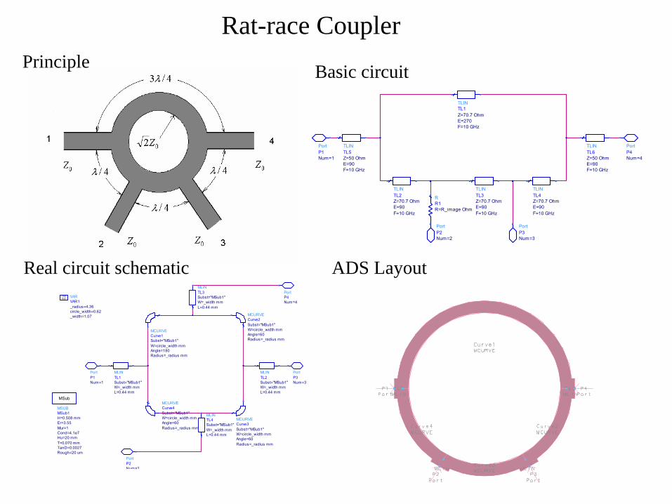
Rat-race Coupler
TLINTL6
F=10 GHzE=90Z=50 Ohm
PortP4Num=4
TLINTL5
F=10 GHzE=90Z=50 Ohm
PortP1Num=1
TLINTL4
F=10 GHzE=90Z=70.7 Ohm
TLINTL3
F=10 GHzE=90Z=70.7 Ohm
TLINTL2
F=10 GHzE=90Z=70.7 Ohm
TLINTL1
F=10 GHzE=270Z=70.7 Ohm
PortP3Num=3
PortP2Num=2
RR1R=R_image Ohm
VARVAR1
_width=1.07circle_width=0.62_radius=4.36
EqnVar
PortP2Num=2
MSUBMSub1
Rough=20 umTanD=0.0027T=0.070 mmHu=20 mmCond=4.1e7Mur=1Er=3.55H=0.508 mm
MSub
MLINTL4
L=0.44 mmW=_width mmSubst="MSub1"
PortP1Num=1
PortP3Num=3
PortP4Num=4
MLINTL2
L=0.44 mmW=_width mmSubst="MSub1"
MCURVECurve3
Radius=_radius mmAngle=60W=circle_width mmSubst="MSub1"
MCURVECurve2
Radius=_radius mmAngle=60W=circle_width mmSubst="MSub1"
MCURVECurve4
Radius=_radius mmAngle=60W=circle_width mmSubst="MSub1"
MCURVECurve1
Radius=_radius mmAngle=180W=circle_width mmSubst="MSub1"
MLINTL3
L=0.44 mmW=_width mmSubst="MSub1"
MLINTL1
L=0.44 mmW=_width mmSubst="MSub1"
Principle
Real circuit schematic ADS Layout
Basic circuit

Wilkinson power divider
TLINTL7
F=10 GHzE=90Z=50 Ohm
TLINTL4
F=10 GHzE=90Z=50 Ohm
TLINTL3
F=10 GHzE=90Z=50 Ohm
PortP1Num=1
RR1R=100 Ohm
TLINTL1
F=10 GHzE=90Z=70.7 Ohm
TLINTL2
F=10 GHzE=90Z=70.7 Ohm
PortP3Num=3
PortP2Num=2
VARVAR1
_length2=1.04503 {o}_length1=2.13804 {o}_length=_radius-circle_width/2+0.26_radius=2.3_width=0.533843 {o}_width2=0.400138 {o}circle_width=0.70009 {o}
EqnVar
MLINTL8
L=0.5 mmW=1.07 mmSubst="MSub1"
MLINTL9
L=0.5 mmW=1.07 mmSubst="MSub1"
MSUBMSub1
Rough=20 umTanD=0.0027T=0.070 mmHu=20 mmCond=4.1e7Mur=1Er=3.55H=0.508 mm
MSub
MTEE_ADSTee1
W3=1.07 mmW2=circle_width mmW1=circle_width mmSubst="MSub1"
MSTEPStep1
W2=_width2 mmW1=1.07 mmSubst="MSub1"
MSTEPStep2
W2=_width2 mmW1=1.07 mmSubst="MSub1"
MLINTL7
L=1 mmW=1.07 mmSubst="MSub1"
MTEE_ADSTee3
W3=_width mmW2=_width2 mmW1=circle_width mmSubst="MSub1"
MTEE_ADSTee2
W3=_width mmW2=_width2 mmW1=circle_width mmSubst="MSub1"
MLINTL6
L=_length2 mmW=_width2 mmSubst="MSub1"
MLINTL5
L=_length2 mmW=_width2 mmSubst="MSub1"
MLINTL3
L=_length1 mmW=circle_width mmSubst="MSub1"
MLINTL4
L=_length1 mmW=circle_width mmSubst="MSub1"
PortP3Num=3
PortP2Num=2
PortP1Num=1
MLINTL2
L=_length mmW=_width mmSubst="MSub1"
R_Pad1R1
L1=0.5 mmS=0.15 mmW=0.4 mmR=100 Ohm
MLINTL1
L=_length mmW=_width mmSubst="MSub1"
MCURVECurve1
Radius=_radius mmAngle=90W=circle_width mmSubst="MSub1"
MCURVECurve2
Radius=_radius mmAngle=90W=circle_width mmSubst="MSub1"
Principle Basic circuit
Real circuit schematic ADS Layout

rein UUU +=
WuZUu
L
== ][; WiZIi L =×= ][;
Lrein ZUUI /)( −=
L
re
L
in
ZUb
ZUa == ,
baibau −=+= ; 2/)(2
)(L
L
ZIZUiua ×+=
+= 2/)(
2)(
LL
ZIZUiub ×−=
−=
22
21;
21 bPaP rein ==
Relative voltage and current:
Wave variables:
So
Power:
wave variable

Appendix B
Tuner with Branchline coupler and SMV 2019-108
Tuner with Branchline coupler and SMV 1245-011

Mixer testing circuit board
System circuit board

Appendix CTuner test results

Appendix DInterpolation
• function v3=interpolation(v1,v2)• userdata = importdata('final.txt');• data = userdata.data;• Ufet=-0.7:0.05:0;• Udiode=0:1:6;• Udc1=data(1:15,3)';• Udc2=data(16:30,3)';• Udc3=data(31:45,3)';• Udc4=data(46:60,3)';• Udc5=data(61:75,3)';• Udc6=data(76:90,3)';• Udc7=data(91:105,3)';• Udc=[Udc1;Udc2;Udc3;Udc4;Udc5;Udc6;Udc7];• v3=interp2(Ufet,Udiode,Udc,v2,v1);• v3=abs(v3);
Optimization
• function [x fval history DC] = func2(x0)• history = [];• options = optimset('OutputFcn', @myoutput);• [x fval] = fminsearch(@(x)
interpolation(x(1),x(2)),x0,options); • function stop = myoutput(x,optimvalues,state);• stop = false;• if state == 'iter'• history = [history; x];• end• end• DC=interpolation(history(:,1),history(:,2));• plot3(history(:,1),history(:,2),DC,'-*')• xlabel('Udiode'),ylabel('Ufet'),zlabel('Udc');• grid on• axis ([0 6 -0.8 0 -2 6])• end