a novel multi-probe resistivity approach to inspect green
TRANSCRIPT

Journal of Nondestructive Evaluation, Vol. 16, No. 4. 1997
A Novel Multi-Probe Resistivity Approach to Inspect Green-State Metal Powder Compacts
J. Stander,1 J. Plunkett,1 W. Michalson,1 J. McNeill,1 and R. Ludwig1
Received February 2, 1997; September 6, 1997
This paper describes a new instrumentation approach to the nondestructive testing of green-statepowdered metallurgy components. These samples are likely to generate surface-breaking and sub-surface defects prior to sintering. Exploiting the principles of electric resistivity or potential dropmeasurements in solids, a system is configured which is capable of recording surface voltagedistributions due to impressed current inputs. At the heart of this novel testing procedure is amultiple-pin sensor which allows for flexible measurement conditions in order to cover wide sur-face areas. Practical tests with production samples compare well with both analytical and numericalmodeling techniques in predicting surface voltage distributions. Furthermore, initial studies ofsurface-breaking flaws exhibit excellent defect detectability.
KEY WORDS: Green-state powder metallurgy compacts; resistivity testing; multi-probe sensor.
1. INTRODUCTION
The nondestructive testing of finished, postsinteredpowdered metallurgy (P/M) parts has primarily relied ontraditional NDE techniques such as ultrasonic and eddycurrent inspections.(1) From a manufacturing point ofview, it is however very desirable to detect the occur-rence of cracks in the compacting stage prior to sinter-ing. At this point, the PM compounds or green partshave been subjected to mechanical compression wherepress alignment, tooling, and material mixtures play amajor role in determining the quality of the final part.(2)
An NDE technique at this stage would permit the inter-ception and modification of the manufacturing processbefore sintering, thus avoiding the production of oftenthousands of faulty end specimens at associated highcosts. Unfortunately very little work has been devotedtoward the inspection of green parts,(3) since the loosely-connected microscopic particle compositions represent
1 Department of Electrical and Computer Engineering, Worcester Pol-ytechnic Institute, Worcester, Massachusetts 01609.
high attenuation to elastic waves. In addition, electro-magnetic properties, primarily the low conductivity, theoften ferrous material nature as well as high surface re-flectivity to heat energy make PM parts not suitable foreddy current and thermal inspections.
The focus of this investigation is concentrating onthe electric resistivity or impedance properties of P/Mparts,(4-7) mainly because
• they possess sufficient conductivity/resistivitywhich can be exploited as a physical qualityparameter,
• the testing methods appear sufficiently robust inthat small production-related changes in materialcomposition such as density variations do notimpede the detection of cracks, and
• the equipment development is not prohibitivelyexpensive.
It is pointed out that this type of testing exploitsspatial changes in conductivity only, i.e., the mechanicalprocesses of compacting and machining must be corre-lated with a single electric material parameter.(8) The as-sociated mathematical task of inverting the underlying
2050195-9298/97/1200-0205$12.50/0 © 1997 Plenum Publishing Corporation

206 Stander, Plunkett, Michalson, McNeill, and Ludwig
problem. Current input and current output to the speci-men are modeled by imposing Neumann-type of bound-ary conditions at point locations on the surface. Theinjected current establishes electric field and potentialdistributions throughout the sample region as well asover the surface. It is the differential voltage betweenpoint contacts on the surface which is of interest sinceit is measured by our instrument. Therefore the startingpoint of the theoretical analysis is Laplace's equation inthe form
where <j>(r) is the voltage distribution, and a representsthe spatially dependent conductivity. The localizedsource current density at discrete surface locations is ap-plied through the boundary condition
Fig. 1. Generic test configuration of a cross-section of a rectangularPM part with point currents located at surface.
while over the remaining surface locations either fluxfree, or potential
conditions are imposed. Since closed-form solutions toEq. (1) can only be found for the simplest geometriccases, numerical methods such as finite difference, finiteelements, boundary elements are employed when real-istic problems have to be investigated. In particular, thefinite element approach converts Eq. (1) into a linearmatrix equation
where [S] contains spatial information regarding CT andvectors {(]>} and {J} denote the unknown nodal potentialand known source distributions throughout the solutiondomain.(2) The nodal potential values {<}>} can subse-quently be processed into voltage distributions <$>(x, z)via suitable local approximation or shape functions.With (|> determined via matrix inversion, the electric fieldE is found through the gradient operation E = -V<|>. Abasic electrostatic test configuration for an unflawedsample of length a is shown in Fig. 1. In this model oneinjects and receives a known current I0 along F, whichis specified as Neumann-type boundary condition. Thelocation of the point current contacts at a/4 and 3a/4 aredescribed by shifted delta functions &(x - a/4) and 8(x- 3a/4) of strength 1% and /o. In addition, the followingboundary conditions are imposed:
elliptic partial differential equations for the unknownconductivity distribution has yielded rather low qualityimages as the medical field has shown.(9)
From an instrumentation point of view, sensitivityand reproducibility have to be established. Key pointsof the investigation include such parameters as flaw sizeand orientation vs. detectable voltage response, numberand placement of sensors, contact needle pressure, cur-rent strength, conductivity variations from sample-to-sample as well as within the individual sample, etc.
In order to aid in the preparation of controlled sam-ples as well as providing data for the instrumentationeffort, a theoretical model attempting to simulate phys-ical reality is necessary. On the basis of the finite ele-ment method, a numerical model has been devisedwhich predicts voltage distributions due to currentsource inputs. Results from this model are subsequentlyemployed to calibrate the voltage recording of the in-strument.
The organization of this paper is as follows: Sect.2 introduces the basic theory and the generic model con-figuration followed by the numerical formulation and itsanalytical verification. Section 3 then discusses the an-alog and digital instrumentation approach which allowsthe recording of surface voltage distributions based onknown current inputs. In Section 4, preliminary mea-surement results of P/M specimens are placed in contextwith the theoretical modeling approach.
2. THEORETICAL BASIS
The DC impedance testing of green-state P/M partscan mathematically be described as a static current flow

Green-State Metal Powder Compacts 207
In order to test the fidelity of the numerical model forthe geometry depicted in Fig. 1, analytical solutions arederived based on a standard Separation of Variable(SOV) approach which yields for boundary conditiontype (4b)
and for boundary condition type (4c)
Fig. 2. Voltage distribution as a function of depth for <$>(x, 0) = 0.
WITwhere an = — and /„, /o are the impressed positive and
anegative currents. Both boundary conditions can easilybe enforced in the experiment by either grounding thebottom surface or by placing the PM sample on an in-sulating contact plane. For instance, with current of +/-1 A, a = 20 cm, c = 5 cm, Fig. 2 shows five typicalvoltage distributions at various depth layers starting fromthe top surface (z = 5 cm) down to z = 4 cm. Figure 3quantifies the effect of sample thickness variations forthe two types of boundary conditions imposed on F4. Asexpected, both solutions (5) and (6) yield the same sur-face voltages for a thick sample (Fig. 3a), but begin todiffer as the sample thickness is reduced (Fig. 3b). Thedrop in maximum voltage signal strength as a functionof depth into the specimen is depicted in Fig. 4 forgrounded F4. Here z = 5 cm corresponds again to thesurface location at the positive current injection point x= a/4 = 5 cm. To appreciate the fidelity of the finiteelement method, Fig. 5 compares the numerical predic-tions with the flux-free voltage distribution of a 5-cm-thick sample.
To extend the numerical model to simulate a sur-face-breaking flaw of 0.5 mm width and 3 mm depth,Fig. 6 shows the surface voltage distribution across theflaw versus the no-flaw situation. Since the flaw is mod-
Fig. 3. Voltage distribution <$>(x, c) for potential fixed (4>(x,0) = 0)and flux free boundary conditions as a function of sample thicknessfor (a) c = 5 cm, and (b) c = 3 cm.

208 Stander, Plunkett, Michalson, McNeill, and Ludwig
Fig. 4. Maximum signal strength as a function of sample depth.Fig. 7. Surface gradient predictions of Fig. 6.
Fig. 5. Comparison between analytical solution (solid line) andnumerical prediction (circles) for flux-free boundary condition.
Fig. 8. Flaw depth as a function of recorded surface voltagegradient.
Fig. 6. Numerical surface voltage prediction for no-flaw and surface-breaking flaw condition.
Fig. 9. Cross-sectional 2-D simulation of a growing subsurface defect.The flaw is initially 1 cm below the surface and extends all the wayto the bottom. The distance flaw tip-sample surface, d, is then reducedto 0.25 cm, 0.15 cm, and 0.025 cm.

Green-State Metal Powder Compacts 209
eled as a discontinuity in conductivity from CT0 = 20 S/mto CT = 0, one observes a localized increase in the surfacevoltage slope. As expected, in moving beyond the flawregion the voltage approaches again the no-flaw distri-bution.
The increase in the surface voltage gradient acrossthe flaw suggests a differential voltage plot as shown inFig. 7 which clearly delineates the flaw location and itsdepth profile. In fact, plotting flaw depth as a functionof peak value of the recorded surface voltage gradientresults in a linear graph as shown in Fig. 8. An increas-ing subsurface flaw is simulated in Fig. 9 where a 0.5-mm-wide and 2-cm-long inclusion is growing toward thesurface in five increments.
3. ANALOG AND DIGITALINSTRUMENTATION
In order to exploit the physical principles of theimpedance measurement technique an instrument hasbeen constructed which is capable of injecting a constantcurrent into the P/M compact and which samples theresulting voltage distribution on the surface accuratelyand repeatably. A key feature of this instrument is a
Fig. 10. Multiprobe sensor consisting of an array of 8 X 8 spring-loaded needles.
multiprobe sensor depicted in Fig. 10. The sensor con-sists of spring-loaded (sharp tip) pins configured in aplanar square array. The outer probes are used to injectcurrent and the inner probes record the voltage distri-
Fig. 11. Sensor in contact with green-state P/M part.

210 Stander, Plunkett, Michalson, McNeill, and Ludwig
Fig. 12. Block diagram of instrument.
bution. Since we rely on differential voltage processing(see Fig. 7), the system has to record signals betweennearest neighbor pins. This configuration yields highflexibility and large surface coverage of the P/M part.To maximize the flaw signal response, the voltage isinitially recorded at an orthogonal direction with respectto the current flow. At present the measurement arrayconsists of an 8 X 8 pin array with a pin-to-pin spacingof 2.54 mm resulting in a 37.6 mm2 planar sensor areawhich contacts the P/M part having a total surface areaof 50 mm X 75 mm (Fig. 11). The spacing is chosen toensure maximum surface coverage while maintainingsufficient measurement accuracy.
To acquire and process these voltages several sys-tem components are required as shown in Fig. 12. AFig. 13. Computed and measured voltage gradient over the surface
of an unflawed P/M part.

Green-State Metal Powder Compacts 211
Fig. 14. Voltage averaging over four production green-state P/M samples in order to establish a baseline.
constant current source injects a DC current of up to 1Ainto the outer pins of the probe. Through a mold theP/M part is positioned accurately under the multipin sen-sor to ensure repeatable measurements from sample tosample. The probe is attached to an arbor press whichmechanically brings the sensor in contact with the partfor good electrical contact. Under computer control sen-sor pins can then be selected for current input as wellas voltage recording. The selection of the various volt-age pins is achieved with the aid of an analog multi-plexer. Because the acquired voltages are on the orderof a few mV, analog signal processing is required toamplify and filter the signals. A 12 bit analog-to-digitalconverter saves the data in files for further digital pro-cessing and display. The software control is handledthrough the Lab View package of National Instruments.
4. MEASUREMENT RESULTS
The instrument was first used to record voltagemeasurements on unflawed samples to establish a base-line and to compare the practical data against the theo-retical modeling predictions. Figure 13 providesmeasured and computed gradient voltages over the sur-
face of a P/M part. Even though the agreement is ingeneral good, one should keep in mind several possibleerror sources. First, the simulation model assumes anhomogeneous sample whereas in reality parts have oftenstatistically known variations in homogeneity. In addi-tion, shape and size of the part can cause edge effectsnot taken into considerations by the theoretical model.Finally, errors associated with small misalignments ofthe probe placement can influence the voltage recording.Since these errors occur in a predictable manner, theycan be taken into account by establishing a baseline asdiscussed below.
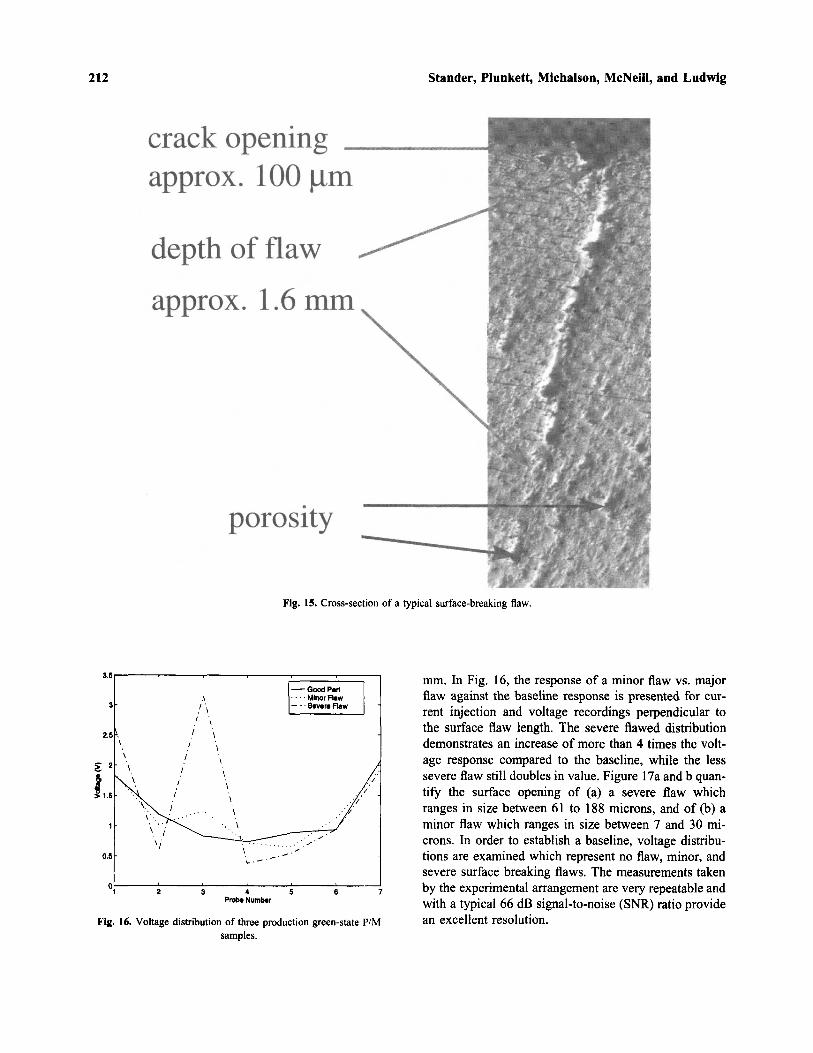
As a next step, the prototype was applied to thetesting of surface breaking flaws in production samples.Since the surface voltage profile, even for unflawed sam-ples, changes slightly from sample-to-sample due to con-tact misalignments and manufacturing-related variationsin density and material composition, a baseline was es-tablished. This can be accomplished by averaging themeasured voltage distribution over several specimens asshown in Fig. 14 for four unflawed samples. To obtainan appreciation of the type of surface-breaking flaw thatcan be detected, Fig. 15 depicts the magnified cross-section of a typical hair-line crack with a surface open-ing of approximately 100 microns and a depth of 1.6
212 Stander, Plunkett, Michalson, McNeill, and Ludwig
Fig. 15. Cross-section of a typical surface-breaking flaw.
Fig. 16. Voltage distribution of three production green-state P/Msamples.
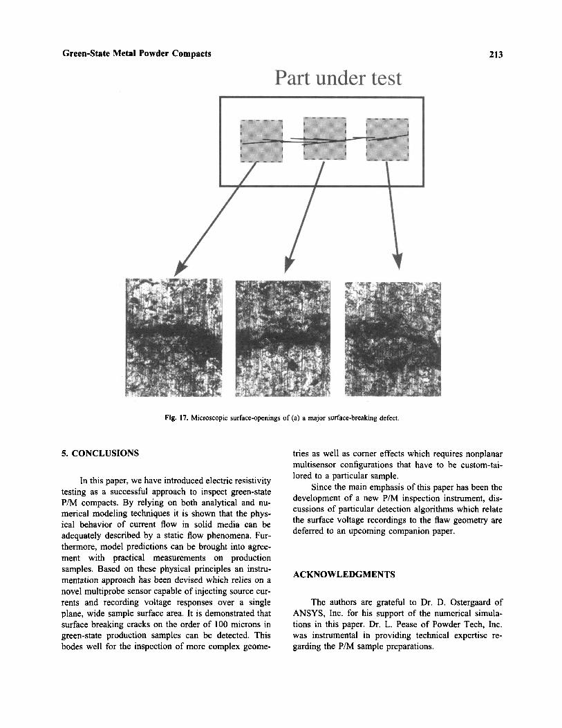
mm. In Fig. 16, the response of a minor flaw vs. majorflaw against the baseline response is presented for cur-rent injection and voltage recordings perpendicular tothe surface flaw length. The severe flawed distributiondemonstrates an increase of more than 4 times the volt-age response compared to the baseline, while the lesssevere flaw still doubles in value. Figure 17a and b quan-tify the surface opening of (a) a severe flaw whichranges in size between 61 to 188 microns, and of (b) aminor flaw which ranges in size between 7 and 30 mi-crons. In order to establish a baseline, voltage distribu-tions are examined which represent no flaw, minor, andsevere surface breaking flaws. The measurements takenby the experimental arrangement are very repeatable andwith a typical 66 dB signal-to-noise (SNR.) ratio providean excellent resolution.
Green-State Metal Powder Compacts 213
Fig. 17. Microscopic surface-openings of (a) a major surface-breaking defect.
5. CONCLUSIONS
In this paper, we have introduced electric resistivitytesting as a successful approach to inspect green-stateP/M compacts. By relying on both analytical and nu-merical modeling techniques it is shown that the phys-ical behavior of current flow in solid media can beadequately described by a static flow phenomena. Fur-thermore, model predictions can be brought into agree-ment with practical measurements on productionsamples. Based on these physical principles an instru-mentation approach has been devised which relies on anovel multiprobe sensor capable of injecting source cur-rents and recording voltage responses over a singleplane, wide sample surface area. It is demonstrated thatsurface breaking cracks on the order of 100 microns ingreen-state production samples can be detected. Thisbodes well for the inspection of more complex geome-
tries as well as corner effects which requires nonplanarmultisensor configurations that have to be custom-tai-lored to a particular sample.
Since the main emphasis of this paper has been thedevelopment of a new P/M inspection instrument, dis-cussions of particular detection algorithms which relatethe surface voltage recordings to the flaw geometry aredeferred to an upcoming companion paper.
ACKNOWLEDGMENTS
The authors are grateful to Dr. D. Ostergaard ofANSYS, Inc. for his support of the numerical simula-tions in this paper. Dr. L. Pease of Powder Tech, Inc.was instrumental in providing technical expertise re-garding the P/M sample preparations.

214 Stander, Plunkett, Michalson, McNeill, and Ludwig
Fig. 17. Continued. Microscopic surface-openings of (b) minor surface breaking defect.
REFERENCES
1. L. F. Pease, Flaw Detection in P/M Parts via Real-Time X-RayAnalysis, Eddy currents and electrical resistivity. InternationalPowder Metallurgy Conference (1988), pp. 478-480.
2. D. Zenger and H. Cai, The Common Cracks in Green P/M Com-pacts Handbook, Powder Metallurgy Research Center Report,Worcester Polytechnic Institute, Worcester, MA (March 1996).
3. L. F. Pease, Crack Detection in Green and Sintered P/M Parts.Presented at the Powder Metallurgy World Congress, San Fran-cisco (June 21-26, 1992).
4. R. L. Cohen and K. W. West, Characterization of metals and al-loys by electrical resistivity measurements, Mater. Eval. 41:1074-1077 (1983).
5. S. Nath, T. J. Rudolphi, and W. Lord, Comparative study of finiteelement and boundary element analysis of the DC potential dropmethod. Mater. Eval. 50:51-55 (1992).
6. A. Lewis and D. Bush, Resistivity measurements of evaluation ofcoating thickness. Mater. Eval. 49:132-135 (1991).
7. H. M. Bauschke and K. H. Schwalbe, Measurement of the depthof surface cracks using the direct current potential drop method.Zeitsch. Werkst. 16:156-165 (1985).
8. E. R. Leheup and J. R. Moon, Electrical conductivity changesduring compaction of pure iron powder. Powder Metall. 4:195-198 (1978).
9. H. M. Powell, D. C. Barber, and I. L. Freeston, Impedance im-aging using linear electrode arrays. Phys. Physiol. Meas. 8:109-118 (1987).
10. A. Uhlir, The potentials of infinite systems of sources and nu-merical solutions of problems in semiconductor engineering. BellSyst. Technol. J. 105-128 (1995).
11. G. H. Aronson and R. O. Ritchie, Optimization of the electricpotential technique for crack growth monitoring on compact testpieces using finite element analysis. J. Test. Eval. 7:208-215(1979).