a 5-gb/s 66 db cmos variable-gain amplifier with
TRANSCRIPT

2169-3536 (c) 2018 IEEE. Translations and content mining are permitted for academic research only. Personal use is also permitted, but republication/redistribution requires IEEE permission. Seehttp://www.ieee.org/publications_standards/publications/rights/index.html for more information.
This article has been accepted for publication in a future issue of this journal, but has not been fully edited. Content may change prior to final publication. Citation information: DOI 10.1109/ACCESS.2018.2867227, IEEEAccess
1
Abstract—This paper proposes a variable gain amplifier (VGA) with reconfigurable DC-offset cancellation (DCOC) for multi-standard applications. In this design, a cell-based design method and some bandwidth extension technologies are adopted to achieve a high data rate and a wide gain control range simultaneously. In addition, the DCOC having a tunable lower-cutoff frequency can make an optimum compromise between BER and SNR according to the specified baseband standard. The measurements show that the VGA achieves a gain control range from -6 dB to 60 dB, a bandwidth beyond 3 GHz, and a tunable lower-cutoff frequency from 0 to 300 kHz. When entering a 223-1 pseudo-random bit sequence (PRBS) signal at 5 Gb/s, the VGA consumes 17 mW from a 1.2-V supply and the output data peak-to-peak jitter is less than 40 ps. The VGA is fabricated in a 90-nm CMOS process with a chip size (including all pads) of 0.52×0.5 mm2.
Index Terms—CMOS VGA, cell-based design, high data rate, reconfigurable, multi-standard applications.
I. INTRODUCTION
CENTLY, the development of wireless transceivers with high data transfer rate has attracted increasing attention
from both the industry and the academia [1]. Among them, the variable-gain amplifier (VGA) as a key module is allocated between RF front-end and baseband circuit to maintain the input signal amplitude within a reasonable range, which can effectively enhance the entire system dynamic range and linearity. In most broadband receivers, the VGA usually operates at low frequency but high data rate (Gb/s). For such applications, a thoughtful circuit design is needed for the VGA to ensure sufficient gain range and wide bandwidth
Fabrication of VGAs in CMOS process remains attractive for low price and ease of integration. However, compared with the high-speed III-V processes such as GaAs or InP, the inferior driving capability and the intrinsic large substrate loss of CMOS severely restrict the design of a high-gain broadband amplifier [2]. For the VGA, these drawbacks have greater impact. Particular limitations are the gain and control range in
a broadband VGA. Besides, the dc offset at the input of the VGA is another critical issue, which needs to be eliminated to avoid saturating the following stages [3]. Therefore, a dc-offset cancellation (DCOC) is required, especially for high gain VGAs [4]. In DCOC, the lower-cutoff frequency (fL) is a key specification for baseband standards [5]. For example, some signals (i.e., random binary or M-ary data) gather the most of energy at dc of the spectrum, they may be corrupted if filtered with a high fL [6]. However, a low fL close to dc may also cause temporary data loss under wrong initial conditions and a long loop settling time [5]. To solve this contradiction, fL should better be adjusted according to the given system requirements. Until now, studies have rarely focused on the DCOC tuning scheme in the VGA design. In [7]-[9], digitally-assisted DCOC methods are provided with an adjustable fL. Nevertheless, an ADC and a DAC are indispensable in the DCOC loop, which makes them unsuitable for high-speed (multi-Gb/s) applications and often consumes a relatively high dc power with increased data rate. Although there are some reconfigurable RF front-end techniques for broadband interface, some insufficiencies have not been solved. In [10], an active RC filter with an array of switched binary-weighted capacitors is adopted. However, it needs a lot of duplicated components to ensure a certain degree of redundancy and thus occupies a large chip area. To resolve this problem, a dual-mode complex filter [11] is realized by the opamp-based RC filter, which only requires less than 20% area occupation for the tuning components. However, it causes a more complex circuit implementation due to the high-order filters. In [12], a programmable complex integrator based on the current division network (CDN) is proposed. It has wider tuning range and higher tuning resolution, but at cost of additional power consumption and more loss in signal path owing to the use of two opamps per integrator.
In this paper, a CMOS VGA with reconfigurable DCOC is presented. By adopting a cell-based design method [13], the limitation on gain-bandwidth product (GBW) of each cascaded variable gain cell is alleviated. Thus, the gain and bandwidth of the whole VGA can be improved simultaneously. Meanwhile, other broadband technologies like the second-order active feedback and the neutralization capacitance are incorporated in the unit variable gain cell (VGC) to further enhance the bandwidth. Besides, the VGA features a reconfigurable DCOC with a voltage controlled lower-cutoff frequency, making it suitable for multi-standard applications.
A 5-Gb/s 66 dB CMOS Variable-Gain Amplifier with Reconfigurable DC-Offset Cancellation for
Multi-standard Applications Zhiqing Liu, Student Member, IEEE, Yunqiu Wu, Member, IEEE, Chenxi Zhao, Member, IEEE,
Johannes Benedikt, and Kai Kang, Member, IEEE
R
This work is supported by National Natural Science Foundation of China
(Grant No. 61331006,61771115), National Science and Technology MajorProject of the Ministry of Science and Technology of China (Grand No.2016ZX03001015-004), Fundamental Research Funds for the CentralUniversities (Grant No. ZYGX2016J036)
Z. Liu, Y. Wu, C. Zhao and K. Kang (corresponding author) are with the School of Electronic Engineering, University of Electronic Science andTechnology of China, Chengdu, China (e-mail: [email protected]).
J. Benedikt is with the School of Engineering, Cardiff University, PrifysgolCaerdydd, United Kingdom.

2169-3536 (c) 2018 IEEE. Translations and content mining are permitted for academic research only. Personal use is also permitted, but republication/redistribution requires IEEE permission. Seehttp://www.ieee.org/publications_standards/publications/rights/index.html for more information.
This article has been accepted for publication in a future issue of this journal, but has not been fully edited. Content may change prior to final publication. Citation information: DOI 10.1109/ACCESS.2018.2867227, IEEEAccess
2
II. CIRCUIT DESIGN AND ANALYSIS
Conventionally, most of wideband VGAs [14]-[16] are realized in a single variable gain stage with cascading one or several fixed gain stages. In this way, the gain range and the bandwidth are mainly determined by the variable gain stage. Besides, in order to make a gain control more efficient and not affecting the common-mode output voltage, the variable gain stage often adopts the Gilbert structure. However, it suffers from a high parasitic capacitance at the output node owing to the cross-coupled differential transistors. To eliminate this effect, Fig. 1 reviews some high-speed Gilbert structures. In Fig.1 (a), a pair of series inductors is adopted as an inductive peaking at the output load terminal [14]. This method can significantly improve the bandwidth. However, an excessive chip area may be required due to the introduction of on-chip inductors, especially when cascading multi-stage of such amplifier. To alleviate the area problem, the active inductor is an alternative to suppress the affect of the parasitic capacitance by introducing impedance peaking at the -3 dB frequency [17]. Fig. 1(b) shows the typical implementation. R1 and C1 together construct a high-pass network so that the high-frequency signal can be bypassed to the gate of transistors M5-8, leading to positive feedback in this active load and thus a gain compensation at high frequency. Although the active inductor can save chip area, it introduces large noise, nonlinearity and additional load capacitance. In addition, since the gain-control transistors M1-2 operate in the triode region, extra nonlinearity may be brought when there is a large signal input, particularly at low-gain state [16]. Fig. 1(c) shows another way to make up the gain loss in high frequency. By introducing peaking in the post amplifiers rather than in the load of the gain core itself [15], a flat frequency response can be achieved if the compensated peaking is situated right in the −3 dB frequency of the variable gain core. However, due to the existence of process and temperature variations, there may be an intolerable peaking for cascaded stages of post amplifiers. Therefore, it is difficult to realize a large gain and gain control range while maintaining a high-speed operation only by using a single variable gain stage.
A. Analysis of the Cell-Based Design Method
For any active device, its GBW is inherently fixed. In other words, if a single-stage amplifier achieves a high gain, then its bandwidth is limited. To solve this contradiction, the single-stage amplifier can be regarded as an individual cell for compromising its gain and bandwidth. Then, making several identical cells cascaded to obtain a high gain and a wide bandwidth simultaneously. Generally, such a cell-based design method has often been employed in an amplifier requiring a wide bandwidth [18]. If this method is applied to the design of a broadband VGA, there is more space for implementation of a large gain control range by adopting a multi-stage structure. Fig. 2 shows the architecture of this cell-based VGA. Assuming that
Fig. 1. (a) Gilbert core with peaking inductor load, (b) differential cascode structure using active inductor load, and (c) Gilbert core using gain-peaking post amplifierfor a fast speed.
Fig. 2. (a) The architecture of the cell-based VGA, and (b) the required GBW vs. the number of stages for Atot = 50 dB and BWtot = 4 GHz.
2169-3536 (c) 2018 IEEE. Translations and content mining are permitted for academic research only. Personal use is also permitted, but republication/redistribution requires IEEE permission. Seehttp://www.ieee.org/publications_standards/publications/rights/index.html for more information.
This article has been accepted for publication in a future issue of this journal, but has not been fully edited. Content may change prior to final publication. Citation information: DOI 10.1109/ACCESS.2018.2867227, IEEEAccess
3
the VGA consists of n VGCs with mth-order Butterworth frequency response, the required GBW of each VGC is [2]
2 2 1
tot nVGC tot
m n
BWGBW A
(1)
where Atot is the overall gain of the cascaded VGCs, BWtot is the overall bandwidth. If Atot=50 dB and BWtot=4 GHz are targeted, the required GBWVGC under m=1, 2, 3 is a decreasing function of stage n as shown in Fig. 2(b). Note that the required GBWVGC
can be alleviated rapidly if using large n and m. However, with the maximum number of stage and order, some practical factors also need to be considered, i.e., power consumption and noise. Power consumption increases with the large n and m. In addition, it results in a reduced gain per stage due to a fixed total gain and thus makes a rapid noise accumulation from the gain stages. As a result, the input-referred noise figure (NF) of the whole VGC stage is significantly degraded. This effect can be quantified by [19]
1 1
1 1 1p p
NF
NF A
(2)
where NF∞ denotes the NF of an infinite number of cascaded gain stages, NFp is the NF of each gain stage and Ap is the gain of each stage. Therefore, n=3 and m=2 are chosen to trade-off power consumption, GBW, and NF in this design.
It is significant to note that the gain range of the VGA can be enlarged effectively by cascading multiple VGCs, but there still exists some challenges in implementation of such a cell. Firstly, the gain error of each cell must be as small as possible to keep the whole accumulated error not exceed the accepted value. Secondly, since a very wideband cell is required due to the gain-bandwidth tradeoff, then some broadband techniques are indispensable for the cell design. Thirdly, the cell should be designed with low power consumption and minimum chip occupation, or else that the total cost of the entire VGA will be excessive. Accordingly, a simple topology is preferred while it is helpful to achieve a wide bandwidth owning to the inherently less parasitic capacitance.
B. Design of the VGC with Extended Bandwidth
The bandwidth of the overall cascaded VGCs is given by 2 2 1m n
tot cellBW BW (3)
where BWcell is the bandwidth of unit VGC. Note that the total bandwidth of the VGA will decrease with the number of n. Thus,
each VGC should have a sufficient bandwidth space to allow for this shrinkage. To enhance the bandwidth of the VGC without sacrificing large chip area or voltage headroom, a second-order gain structure with active feedback is employed. Fig. 3 shows the schematic, where G1, G2 are the gain stages and Gf is the feedback stage. The Gf consists of a differential pair (M5~M6) with a shared resistive load R1 to make a trade-off between bandwidth and gain.
For the convenience of analysis, both the gain and feedback stages can be expressed by the single-pole response functions:
1 2( ) ( )1
mG RG s G s
sRC
(4)
( )1
mff
G RG s
sRC
(5)
where R is the resistive load, C is the parasitic capacitance of the differential pairs, and the corresponding transconductances of the stages are Gm and Gmf. Since a fraction of output signal is returned to the input of G1 by Gf, the transfer function of the second-order VGC is thus given by
2nd
2 2
2 2
20
20 0
( )(1 )
(1 )
m
m mf
G RH s
sRC G G R
A
s A
(6)
where 0=1/RC, A0=GmR and =GmfR. So the first dominant pole is
1 0 0(1 )p A (7)
Fig. 3. Schematic of the 2-order VGC using active feedback.
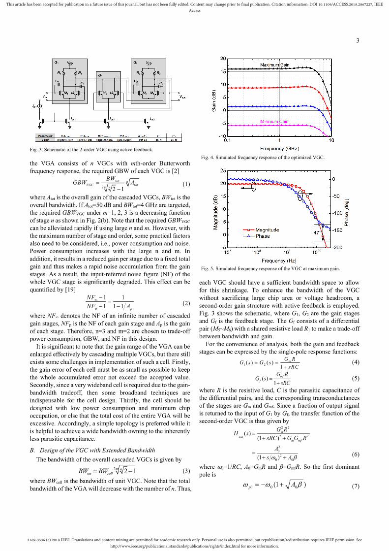
Fig. 4. Simulated frequency response of the optimized VGC.
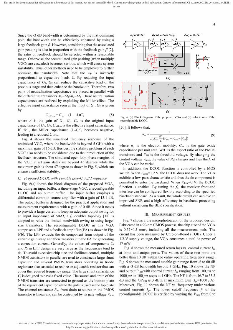
Fig. 5. Simulated frequency response of the VGC at maximum gain.
2169-3536 (c) 2018 IEEE. Translations and content mining are permitted for academic research only. Personal use is also permitted, but republication/redistribution requires IEEE permission. Seehttp://www.ieee.org/publications_standards/publications/rights/index.html for more information.
This article has been accepted for publication in a future issue of this journal, but has not been fully edited. Content may change prior to final publication. Citation information: DOI 10.1109/ACCESS.2018.2867227, IEEEAccess
4
Since the -3 dB bandwidth is determined by the first dominant pole, the bandwidth can be effectively enhanced by using a large feedback gain . However, considering that the associated gain peaking is also in proportion with the feedback gain [2], the ratio of feedback should be selected within a reasonable range. Otherwise, the accumulated gain peaking (when multiply VGCs are cascaded) becomes serious, which will cause system instability. Thus, other methods need to be employed to further optimize the bandwidth. Note that the 0 is inversely proportional to capacitive loads C. By reducing the input capacitance of G1, G2 can reduce the capacitive load of the previous stage and then enhance the bandwidth. Therefore, two pairs of neutralization capacitance are placed in parallel with the differential transistors M1~M2/M3~M4. These neutralization capacitances are realized by exploiting the Miller-effect. The effective input capacitance seen at the input of G1, G2 is given by
1= (1 )eff in inC C A C (8)
where A is the gain of G1, G2, Cin is the original input capacitance of G1, G2, C’
eff-in is the effective input capacitance. If A>1, the Miller capacitance (1-A)C1 becomes negative, leading to a reduced C’
eff-in. Fig. 4 shows the simulated frequency response of the
optimized VGC, where the bandwidth is beyond 5 GHz with a maximum gain of 16 dB. Besides, the stability problem of each VGC also needs to be considered due to the introduction of the feedback structure. The simulated open-loop phase margins of the VGC at all gain states are beyond 45 degrees while the maximum gain is about 47 degree as shown in Fig. 5, which can ensure a sufficient stability.
C. Proposed DCOC with Tunable Low-Cutoff Frequency
Fig. 6(a) shows the block diagram of the proposed VGA, including an input buffer, a three-stage VGC, a reconfigurable DCOC and an output buffer. The input buffer employs a differential common-source amplifier with a gain of 13.1 dB. The output buffer is designed for the practical application and measurement requirements with a gain of 0 dB. Since it needs to provide a large current to keep an adequate output swing for an input impedance of 50-Ω, a fT doubler topology [18] is adopted to relax the limited bandwidth owing to using large-size transistors. The reconfigurable DCOC in this VGA comprises a LPF and a feedback amplifier (FA) as shown in Fig. 6(b). The LPF extracts the dc component from output of the variable gain stage and then transfers it to the FA for generating a correction current. Generally, the values of components Cf and Rf in LPF design are very large as the frequencies tend to dc. To avoid excessive chip size and facilitate control, multiple NMOS transistors in parallel are used to construct a large shunt capacitor and several PMOS transistors operating in triode region are also cascaded to realize an adjustable resistor that can cover the required frequency range. The large shunt capacitance Cf is designed to have a fixed value. The source and drain of the NMOS transistor are connected to ground as the bottom plate of the equivalent capacitor while the gate is used as the top plate. The channel resistance Ron from drain to source in the PMOS transistor is linear and can be controlled by its gate voltage Vtune
[20]. It follows that, 1
( )on
p ox DD tune TH
RW
C V V VL
(9)
where μp is the electron mobility, Cox is the gate oxide capacitance per unit area, W/L is the aspect ratio of the PMOS transistors and VTH is the threshold voltage. By changing the control voltage Vtune, the value of Ron changes and then the fL of the VGA can be varied.
In addition, the DCOC function is controlled by a MOS switch. When Vdcoc=1.2 V, the DCOC does not work. The VGA exhibits a low-pass characteristic and thus the dc component is permitted to enter the baseband. When Vdcoc=0 V, the DCOC function is enabled. By tuning the fL, the receiver front-end interface can be configured flexibly according to the specified baseband standard. As a result, the whole circuit can achieve an improved SNR and a high efficiency in baseband processing without sacrificing the BER specification.
III. MEASUREMENT RESULTS
Fig. 7 shows a die microphotograph of the proposed design. Fabricated in a 90-nm CMOS process, the chip size of the VGA is 0.52×0.5 mm2, including all the measurement pads. The circuit has been measured by Chip-on-Board (COB). Under a 1.2-V supply voltage, the VGA consumes a total dc power of 17 mW.
Fig. 8 shows the measured return loss vs. control current Igc at input and output ports. The values of these two ports are better than 10 dB within the entire operating frequency range. Fig. 9 shows the measured tunable gain range from -6 to 60 dB with a -3 dB bandwidth beyond 3 GHz. Fig. 10 shows the NF and output P1dB with control current Igc ranging from 100 μA to 1000 μA in 100 μA steps at 1 GHz. The NF is from 16.7 to 33.5 dB and the OP1dB is 3 dBm at maximum gain (Igc=1000 μA). Moreover, Fig. 11 shows the NF vs. frequency under various control currents Igc. The lower cutoff frequency fL of the reconfigurable DCOC is verified by varying the Vtune from 0 to
Fig. 6. (a) Block diagram of the proposed VGA and (b) sub-circuits of the reconfigurable DCOC.

2169-3536 (c) 2018 IEEE. Translations and content mining are permitted for academic research only. Personal use is also permitted, but republication/redistribution requires IEEE permission. Seehttp://www.ieee.org/publications_standards/publications/rights/index.html for more information.
This article has been accepted for publication in a future issue of this journal, but has not been fully edited. Content may change prior to final publication. Citation information: DOI 10.1109/ACCESS.2018.2867227, IEEEAccess
5
1 V after activating this function (Vdcoc=0 V). The obtained fL at different gains are shown in Fig. 12. The output eye diagram and data jitter of the VGA are characterized by a Tektronix AWG7000 arbitrary waveform generator and a Tektronix MSO71604C oscilloscope. Fig. 13 shows the output eye diagrams under 5 Gb/s 223-1 PRBS signals with different input swings. Both of them have a vertical eye opening larger than 300 mV. Under an input signal level of 20 mV, the peak-to- peak jitter for 5 Gb/s is 39 ps.
Table I summarizes and compares the performance of this VGA with other previous reported works [15]-[16], [21]-[24]. The proposed VGA has wider bandwidth, larger gain and gain
control range as compared to the works [21]-[24]. Although the design in [15]-[16] has an excellent data rate than the proposed VGA design, they occupy a relatively large power consumption and chip area. Moreover, this work realizes a reconfigurable DCOC, attaining a tunable lower cutoff frequency range.
IV. CONCLUSION
A CMOS variable gain amplifier with reconfigurable DCOC for multi-standard applications has been demonstrated in this work. Since a cell-based design method and some bandwidth extension technologies are adopted, a gain control range of 66 dB and a data rate up to 5 Gb/s are achieved simultaneously
Fig. 7. Die photo of the fabricated VGA.
Fig. 8. Measured return loss vs. various control currents Igc at input and outputports.
Fig. 9. Measured voltage gain in various control currents Igc vs. frequency.
Fig. 10. Measured NF and OP1dB at 1 GHz vs. various control currents Igc.
Fig. 11. Measured NF vs. frequency under various control currents Igc.
Fig. 12. Measured fL of the reconfigurable DCOC vs. Vtune at different gains.

2169-3536 (c) 2018 IEEE. Translations and content mining are permitted for academic research only. Personal use is also permitted, but republication/redistribution requires IEEE permission. Seehttp://www.ieee.org/publications_standards/publications/rights/index.html for more information.
This article has been accepted for publication in a future issue of this journal, but has not been fully edited. Content may change prior to final publication. Citation information: DOI 10.1109/ACCESS.2018.2867227, IEEEAccess
6
with a small data jitter of 39 ps. Moreover, the reconfigurable DCOC with tunable fL from 0 to 300 kHz provides an optimum compromise between BER and SNR requirements of the specified baseband standard. Accordingly, the VGA can be well utilized in high-speed transceiver systems sustaining multiple baseband standards. Meanwhile, its design concepts with non-passive inductor topology can be also easily migrated to more advanced CMOS technologies (e.g., 40 nm or 28 nm) for further improving bandwidth and data rate without robustness concerns and sacrificing other performances.
REFERENCES [1] Y. Yu, H. Liu, Y. Wu, and K. Kang, “A 54.4–90 GHz Low-Noise
Amplifier in 65-nm CMOS,” IEEE J. Solid-State Circuits, vol. 52, no. 11, pp. 2892–2904, Nov. 2017.
[2] H.- Y. Huang, J.-C. Chien and L.-H. Lu, “A 10-Gb/s Inductorless CMOS Limiting Amplifier With Third-Order Interleaving Active Feedback,” IEEE J. Solid-State Circuits, vol. 42, no. 5, pp. 1111–1120, May. 2007.
[3] K. Kang, F. J. Lin, D.-D. Pham, J. Brinkhoff, C.-H. Heng, Y. X. Guo and X. J. Yuan, “A 60-GHz OOK Receiver With an On-chip Antenna in 90
nm CMOS,” IEEE J. Solid-State Circuits, vol. 45, no. 9, pp. 1720–1730, Sep. 2010.
[4] Y. Wang, B. Afshar, T.-Y. Cheng, V. Gaudet, and A. Niknejad, “A 2.5mW Inductorless Wideband VGA with Dual Feedback DC-Offset Correction in 90 nm CMOS Technology,” in Proc. IEEE Radio Freq. Integr. Circuits Symp., 2008, pp. 91–94.
[5] A. Emira, A. Valdes-Garcia, B. Xia, A. Mohieldin, A. Valero-Lopez, S. Moon, C. Xin, and E. Sanchez-Sinencio, “Chameleon: A Dual-mode 802.11b/Bluetooth Receiver System Design,” IEEE Trans. Circuits Syst. I, Reg. Papers, vol. 53, no. 5, pp. 992–1003, May 2006.
[6] B. Razavi, “Design Considerations for Direct-Conversion Receivers,” IEEE Trans. Circuits Syst. II, Analog Digit. Signal Process, vol. 44, no. 6, pp. 428–435, Jun. 1997.
[7] G. Retz, et al., “A Highly Integrated Low-Power 2.4GHz Transceiver Using a Direct-Conversion Diversity Receiver in 0.18um CMOS for IEEE802.15.4 WPAN,” in IEEE ISSCC, Feb. 2009, pp. 414-415.
[8] H. Okuni, et al., “A Direct Conversion Receiver with Fast-Settling DC Offset Canceller,” in IEEE Symp. PIMRC, 2007, pp. 1-5.
[9] H. Yoshida, et al., “DC Offset Canceller in a Direct Conversion Receiver for QPSK Signal Reception,” in IEEE Symp. PIMRC, 1998, pp.1314-1318.
[10] H. Darabi, J. Chiu, S. Khorram, H. J. Kim, Z. Zhou, H.-M. Chien, B. Ibrahim, E. Geronaga, L. H. Tran, and A. Rofougaran, “A Dual-mode 802.11b/bluetooth Radio in 0.35 µm CMOS,” IEEE J. Solid-State Circuits, vol. 40, no. 3, pp. 698–706, Mar. 2005.
[11] T. Cho, D. Kang, C. Heng, and B. Song, “A 2.4 GHz Dual-mode 0.18 µm CMOS Transceiver for Bluetooth and 802.11b,” IEEE J. Solid-State Circuits, vol. 39, no. 11, pp. 1916–1926, Nov. 2004.
[12] H. A. Alzaher, “A CMOS Highly Linear Digitally Programmable Active-RC Design Approach,” IEEE Trans. Circuits Syst. I, Reg. Papers, vol. 58, no. 11, pp. 2636–2646, Nov. 2011.
[13] H. Liu, X. Zhu, C. C. Boon, X. F. He, “Cell-Based Variable Gain Amplifiers with Accurate dB-Linear Characteristic in 0.18-um CMOS Technology,” IEEE J. Solid-State Circuits, vol. 50, no. 2, pp. 586-596, Feb. 2015.
[14] C.-F. Liao and S.-L. Liu, “A 10 Gb/s CMOS AGC Amplifier with 35 dB Dynamic Range for 10Gb Ethernet,” in IEEE ISSCC Dig. Tech. Papers, Feb. 2006, pp. 2092–2101.
[15] C. Liu, Y.-P. Yan, W.-L. Goh, Y.-X. Xiong, L.-J. Zhang and M. Madihian, “A 5-Gb/s Automatic Gain Control Amplifier With Temperature Compensation,” IEEE J. Solid-State Circuits, vol. 47, no. 6, pp. 1323–1333, Jun. 2012.
[16] S. Ray and M. -M. Hella, “A 10 Gb/s Inductorless AGC Amplifier With 40 dB Linear Variable Gain Control in 0.13 µm CMOS,” IEEE J. Solid-State Circuits, vol. 51, no. 2, pp. 440–456, Feb. 2016.
[17] H. D. Lee, K. A. Lee, and S. Hong, “A Wideband CMOS Variable Gain Amplifier with an Exponential Gain Control,” IEEE Trans. Microw. Theory Techn., vol. 55, no. 6, pp. 1363–1373, Jun. 2007.
[18] S. Galal and B. Razavi, “10-Gb/s Limiting Amplifier and Laser/modulator Driver in 0.18-µm CMOS technology,” IEEE J. Solid-State Circuits, vol. 38, no. 12, pp. 2138–2146, Dec. 2003.
TABLE I PERFORMANCE COMPARISON OF THE STATE-OF-THE-ART VGAS
Ref. Tech. Control mode
Freq. (GHz)
Gain range (dB)
Data rate(Gb/s)
NF (dB)
Jitter(pp)
OP1dB
(dBm) Reconfig.
DCOC Power (mW)
Chip Area (mm2)
[15] 2012 JSSC
0.13-μm SiGe BiCMOS
Analog voltage
0.0002-7.5 -10 to 30 5 -- 40 ps - N 72*@1.2V 1*
[21] 2012 TCSI
90-nm CMOS
Analog voltage
0.0002-2.2 -10 to 50 - 17 to 30 - -3 N 2.5 @1.0V 0.7
[22] 2013 RFIC
65-nm CMOS
Digital current
0.02-1 +3 to +31 - 6 to 21 - 0 N 48 @1.1V 1**
[23] 2014 TMTT
0.18-μm SiGe BiCMOS
Digital current
0.003-1.17 -1.4 to 30.2 2 24 to 52 - -10 N 35 @1.8V 0.25***
[24] 2016 MWCL
65-nm CMOS
Analog current
(0~0.0002)-4
-39.4 to 20.2 - 10 to 27 - -9.8 Y 26 @1.2V 0.32
[16] 2016 JSSC
0.13-μm CMOS
Analog voltage
0.0001-5 -15 to 25 10 - 44 ps - N 50 @1.2V 1.07
[25] 2016 TMTT
65-nm CMOS
Analog voltage
0.0004-2 2 to 24 - 24 to 29 - 1.8 N 3.5*** @
1.2V 0.01***
This work 90-nm CMOS
Analog current
(0~0.0003)-3.3
-6 to 60 5 15.2 to 29 39 ps 3 Y
(0-300kHz) 17 @1.2V 0.26
*=With Temperature Compensation Block; **=With Digital Control; ***= VGA core only
Fig. 13. Measured output eye diagram at (a) 5 mVpp, (b) 20 mVpp, 5 Gb/s 223-1 PRBS input data (Horizontal scale: 50 ps/div, Vertical scale: 100 mV/div).

2169-3536 (c) 2018 IEEE. Translations and content mining are permitted for academic research only. Personal use is also permitted, but republication/redistribution requires IEEE permission. Seehttp://www.ieee.org/publications_standards/publications/rights/index.html for more information.
This article has been accepted for publication in a future issue of this journal, but has not been fully edited. Content may change prior to final publication. Citation information: DOI 10.1109/ACCESS.2018.2867227, IEEEAccess
7
[19] R. P. Jindal, “Gigahertz-Band High-Gain Low-Noise AGC Amplifiers in Fine-Line NMOS,” IEEE J. Solid-State Circuits, vol. SC-22, pp. 512–521, Aug. 1987.
[20] B. Razavi, Design of Analog CMOS Integrated Circuits. Xian, China: Xian Jiaotong University Press, 2002.
[21] Y. Wang, B. Afshar, Y. Lu, V. C. Gaudet, and A. M. Niknejad, “Design of A Low Power, Inductorless Wideband Variable-gain Amplifier for Highspeed Receiver Systems,” IEEE Trans. Circuits Syst. I, Reg. Papers, vol. 59, no. 4, pp. 696–707, Apr. 2012.
[22] Y. Wang, C. Hull, G. Murata, and S. Ravid, “A Linear-in-dB Analog Baseband Circuit for Low Power 60 GHz Receiver in Standard 65 nm CMOS,” in Proc. IEEE Radio Freq. Integr. Circuits Symp., Seattle, WA, 2013, pp. 225–228.
[23] T.-B. Kumar, K. Ma, K.-S. Yeo, and W. Yang, “A 35-mW 30-dB Gain Control Range Current Mode Linear-in-Decibel Programmable Gain Amplifier with Bandwidth Enhancement,” IEEE Trans. Microw. Theory Techn., vol. 62, no. 12, pp. 3465–3475, Feb. 2014.
[24] T.-B. Kumar, et al., “A 4 GHz 60 dB Variable Gain Amplifier with Tunable DC Offset Cancellation in 65 nm CMOS,” IEEE Microw. Wireless Compon. Lett., vol. 25, no. 1, pp. 37–39, Oct. 2015.
[25] H. Liu, C.-C. Boon, X. He, X. Zhu, X. Yi, L. Kong and M.-C Heimlich, “A Wideband Analog-Controlled Variable-Gain Amplifier With dB-Linear Characteristic for High-Frequency Applications,” IEEE Trans. Microw. Theory Techn., vol. 64, no. 2, pp. 533–540, Feb. 2016.