9.5 Ω ron, ±15 v/+12 v/±5 v icmos, serially-controlled ... Ω r on, ±15 v/+12 v/±5 v icmos,...
TRANSCRIPT
9.5 Ω RON, ±15 V/+12 V/±5 V iCMOS, Serially-Controlled Octal SPST Switches
Data Sheet ADG1414
Rev. B Document Feedback Information furnished by Analog Devices is believed to be accurate and reliable. However, no responsibility is assumed by Analog Devices for its use, nor for any infringements of patents or other rights of third parties that may result from its use. Specifications subject to change without notice. No license is granted by implication or otherwise under any patent or patent rights of Analog Devices. Trademarks and registered trademarks are the property of their respective owners.
One Technology Way, P.O. Box 9106, Norwood, MA 02062-9106, U.S.A.Tel: 781.329.4700 ©2009–2015 Analog Devices, Inc. All rights reserved. Technical Support www.analog.com
FEATURES SPI interface Supports daisy-chain mode 9.5 Ω on resistance at 25°C and ±15 V dual supply 1.6 Ω on-resistance flatness at 25°C and ±15 V dual supply Fully specified at ±15 V, +12 V, ±5 V 3 V logic-compatible inputs Rail-to-rail operation 24-lead TSSOP and 24-lead, 4 mm × 4 mm LFCSP
APPLICATIONS Automatic test equipment Data acquisition systems Battery-powered systems Sample-and-hold systems Audio signal routing Video signal routing Communication systems
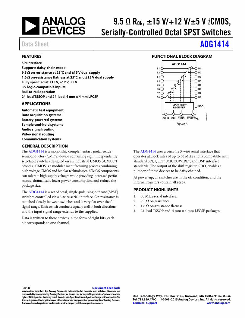
FUNCTIONAL BLOCK DIAGRAM
D8
SDO
D7
D6
D5
D4
D3
D2
D1
S8
S7
S6
S5
S4
S3
S2
S1
INPUT SHIFTREGISTER
SCLK DIN SYNC RESET/VL
ADG1414
0849
7-0
01
Figure 1.
GENERAL DESCRIPTION The ADG1414 is a monolithic complementary metal-oxide semiconductor (CMOS) device containing eight independently selectable switches designed on an industrial CMOS (iCMOS®) process. iCMOS is a modular manufacturing process combining high voltage CMOS and bipolar technologies. iCMOS components can tolerate high supply voltages while providing increased perfor-mance, dramatically lower power consumption, and reduce the package size.
The ADG1414 is a set of octal, single-pole, single-throw (SPST) switches controlled via a 3-wire serial interface. On resistance is matched closely between switches and is very flat over the full signal range. Each switch conducts equally well in both directions and the input signal range extends to the supplies.
Data is written to these devices in the form of eight bits; each bit corresponds to one channel.
The ADG1414 uses a versatile 3-wire serial interface that operates at clock rates of up to 50 MHz and is compatible with standard SPI, QSPI™, MICROWIRE™, and DSP interface standards. The output of the shift register, SDO, enables a number of these devices to be daisy chained.
At power-up, all switches are in the off condition, and the internal registers contain all zeros.
PRODUCT HIGHLIGHTS 1. 50 MHz serial interface. 2. 9.5 Ω on resistance. 3. 1.6 Ω on-resistance flatness. 4. 24-lead TSSOP and 4 mm × 4 mm LFCSP packages.
ADG1414 Data Sheet
Rev. B | Page 2 of 19
TABLE OF CONTENTS Features .............................................................................................. 1 Applications ....................................................................................... 1 Functional Block Diagram .............................................................. 1 Product Highlights ........................................................................... 1 Revision History ............................................................................... 2 Specifications ..................................................................................... 3
±15 V Dual Supply ....................................................................... 3 12 V Single Supply ........................................................................ 4 ±5 V Dual Supply ......................................................................... 6 Continuous Current per Channel .............................................. 7 Timing Characteristics ................................................................ 8
Absolute Maximum Ratings ............................................................ 9 Thermal Resistance ...................................................................... 9
ESD Caution...................................................................................9 Pin Configurations and Function Descriptions ......................... 10 Typical Performance Characteristics ........................................... 12 Test Circuits ..................................................................................... 15 Terminology .................................................................................... 17 Theory of Operation ...................................................................... 18
Serial Interface ............................................................................ 18 Input Shift Register .................................................................... 18 Power-On Reset .......................................................................... 18 Daisy Chaining ........................................................................... 18
Outline Dimensions ....................................................................... 19 Ordering Guide .......................................................................... 19
REVISION HISTORY 11/15—Rev. A to Rev. B Changes to VDD/VSS Parameter, Table 2 ......................................... 5 Updated Outline Dimensions ....................................................... 19 1/13—Rev. 0 to Rev. A Changes to RESET/VL Pin Description Column, Table 9 ......... 11 Changes to Power-On Reset Section ............................................ 19 Updated Outline Dimensions ....................................................... 20 10/09—Revision 0: Initial Version
Data Sheet ADG1414
Rev. B | Page 3 of 19
SPECIFICATIONS ±15 V DUAL SUPPLY VDD = 15 V ± 10%, VSS = −15 V ± 10%, VL = 2.7 V to 5.5 V, GND = 0 V, unless otherwise noted.
Table 1.
Parameter +25°C −40°C to +85°C
−40°C to +125°C Unit Test Conditions/Comments
ANALOG SWITCH Analog Signal Range VSS to VDD V On Resistance (RON) 9.5 Ω typ VDD = +13.5 V, VSS = −13.5 V, VS = ±10 V,
IS = −10 mA; see Figure 23 11.5 14 16 Ω max On-Resistance Match Between Channels (ΔRON) 0.55 Ω typ VDD = +13.5 V, VSS = −13.5 V, VS = ±10 V,
IS = −10 mA 1 1.5 1.7 Ω max
On-Resistance Flatness (RFLAT (ON)) 1.6 Ω typ VDD = +13.5 V, VSS = −13.5 V, VS = ±10 V, IS = −10 mA
1.9 2.15 2.3 Ω max LEAKAGE CURRENTS VDD = +16.5 V, VSS = −16.5 V
Source Off Leakage, IS (Off ) ±0.05 nA typ VS = ±10 V, VD = ∓10 V; see Figure 24 ±0.15 ±1 ±2 nA max Drain Off Leakage, ID (Off ) ±0.05 nA typ VS = ±10 V, VD = ∓10 V; see Figure 24 ±0.15 ±1 ±2 nA max Channel On Leakage, ID, IS (On) ±0.1 nA typ VS = VD = ±10 V; see Figure 25 ±0.3 ±2 ±4 nA max
DIGITAL INPUTS Input High Voltage (VINH) 2.0 V min Input Low Voltage (VINL) 0.8 V max Input Current ±0.001 µA typ VIN = VGND or VL ±0.1 µA max Digital Input Capacitance (CIN) 4 pF typ
LOGIC OUTPUTS (SDO) Output Low Voltage (VOL)1 0.4 V max ISINK = 3 mA 0.6 V max ISINK = 6 mA High Impedance Leakage Current 0.001 µA typ ±1 µA max High Impedance Output Capacitance1 4 pF typ
DYNAMIC CHARACTERISTICS1 tON 75 ns typ RL = 100 Ω, CL = 35 pF 93 110 120 ns max VS = 10 V; see Figure 30 tOFF 25 ns typ RL = 100 Ω, CL = 35 pF 35 35 35 ns max VS = 10 V; see Figure 30 Charge Injection 10 pC typ VS = 0 V, RS = 0 Ω, CL = 1 nF; see Figure 31 Off Isolation −73 dB typ RL = 50 Ω, CL = 5 pF, f = 1 MHz; see Figure 26 Channel-to-Channel Crosstalk −75 dB typ RL = 50 Ω, CL = 5 pF, f = 1 MHz; see Figure 27 Total Harmonic Distortion (THD + N) 0.05 % typ RL = 110 Ω, 15 V p-p, f = 20 Hz to 20 kHz;
see Figure 29 −3 dB Bandwidth 256 MHz typ RL = 50 Ω, CL = 5 pF; see Figure 28 Insertion Loss 0.55 dB typ RL = 50 Ω, CL = 5 pF, f = 1 MHz; see Figure 28 CD, CS (Off ) 8 pF typ f = 1 MHz CD, CS (On) 32 pF typ f = 1 MHz
ADG1414 Data Sheet
Rev. B | Page 4 of 19
Parameter +25°C −40°C to +85°C
−40°C to +125°C Unit Test Conditions/Comments
POWER REQUIREMENTS VDD = +16.5 V, VSS = −16.5 V IDD 0.001 µA typ Digital inputs = 0 V or VL 1 µA max IL Inactive 0.3 µA typ Digital inputs = 0 V or VL 1 µA max IL Active at 30 MHz 0.26 mA typ Digital inputs toggle between 0 V and VL 0.3 0.35 mA max IL Active at 50 MHz 0.42 mA typ Digital inputs toggle between 0 V and VL 0.5 0.55 mA max ISS 0.001 µA typ Digital inputs = 0 V or VL 1 µA max VDD/VSS ±4.5/±16.5 V min/max
1 Guaranteed by design, not subject to production test.
12 V SINGLE SUPPLY VDD = 12 V ± 10%, VSS = 0 V, VL = 2.7 V to 5.5 V, GND = 0 V, unless otherwise noted.
Table 2.
Parameter +25°C −40°C to +85°C
−40°C to +125°C Unit Test Conditions/Comments
ANALOG SWITCH Analog Signal Range 0 to VDD V On Resistance (RON) 18 Ω typ VDD = 10.8 V, VSS = 0 V; VS = 0 V to 10 V,
IS = −10 mA; see Figure 23 21.5 26 28.5 Ω max On-Resistance Match Between Channels (ΔRON) 0.55 Ω typ VDD = 10.8 V, VSS = 0 V; VS = 0 V to 10 V,
IS = −10 mA 1.2 1.6 1.8 Ω max
On-Resistance Flatness (RFLAT (ON)) 5 Ω typ VDD = 10.8 V, VSS = 0 V; VS = 0 V to 10 V, IS = −10 mA
6 6.9 7.3 Ω max LEAKAGE CURRENTS VDD = 10.8 V
Source Off Leakage, IS (Off ) ±0.02 nA typ VS = 1 V/10 V, VD = 10 V/1 V; see Figure 24 ±0.15 ±1 ±2 nA max Drain Off Leakage, ID (Off ) ±0.02 nA typ VS = 1 V/10 V, VD = 10 V/1 V; see Figure 24
±0.15 ±1 ±2 nA max Channel On Leakage, ID, IS (On) ±0.05 nA typ VS = VD = 1 V or 10 V; see Figure 25
±0.3 ±2 ±4 nA max DIGITAL INPUTS
Input High Voltage (VINH) 2.0 V min Input Low Voltage (VINL) 0.8 V max Input Current ±0.001 µA typ VIN = VGND or VL ±0.1 µA max Digital Input Capacitance (CIN) 4 pF typ
LOGIC OUTPUTS (SDO) Output Low Voltage (VOL)1 0.4 V max ISINK = 3 mA 0.6 V max ISINK = 6 mA High Impedance Leakage Current ±1 µA max High Impedance Output Capacitance1 4 pF typ
Data Sheet ADG1414
Rev. B | Page 5 of 19
Parameter +25°C −40°C to +85°C
−40°C to +125°C Unit Test Conditions/Comments
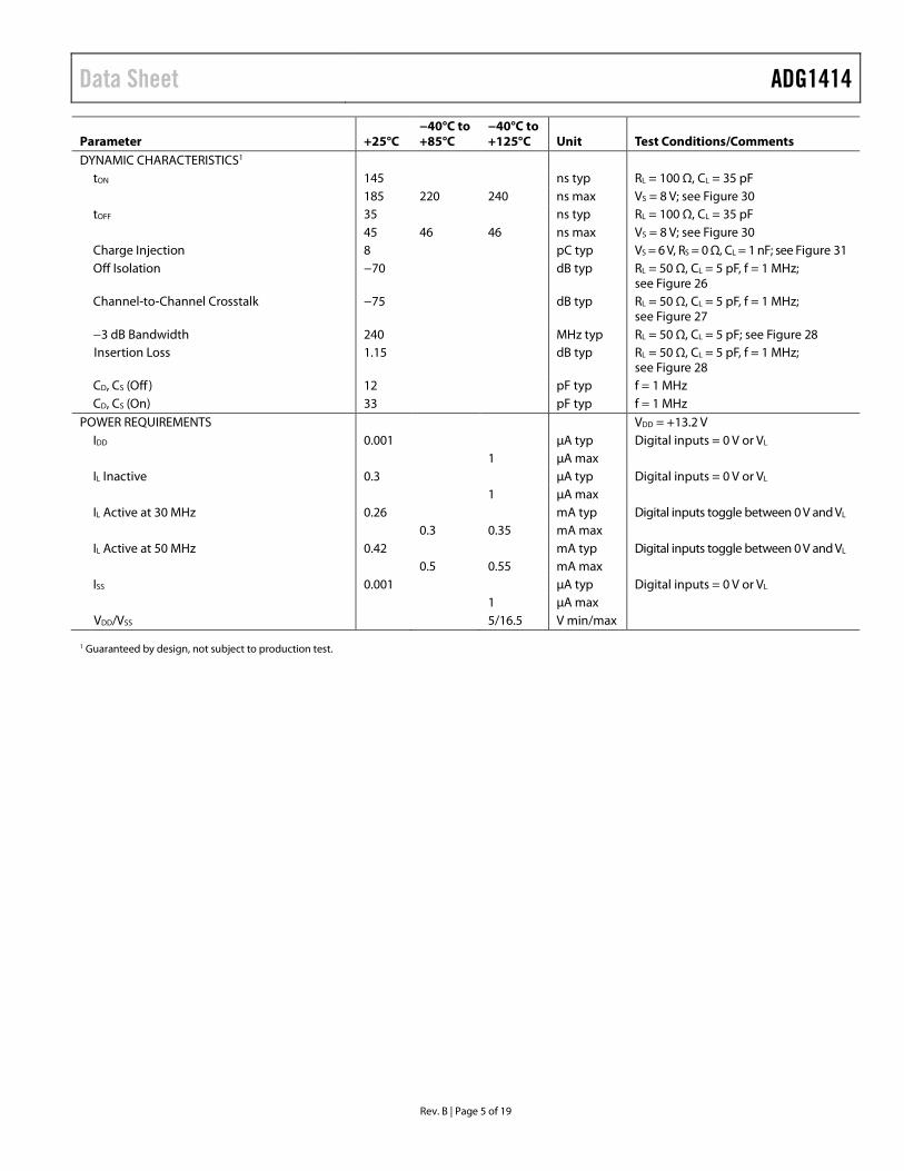
DYNAMIC CHARACTERISTICS1 tON 145 ns typ RL = 100 Ω, CL = 35 pF 185 220 240 ns max VS = 8 V; see Figure 30 tOFF 35 ns typ RL = 100 Ω, CL = 35 pF
45 46 46 ns max VS = 8 V; see Figure 30 Charge Injection 8 pC typ VS = 6 V, RS = 0 Ω, CL = 1 nF; see Figure 31 Off Isolation −70 dB typ RL = 50 Ω, CL = 5 pF, f = 1 MHz;
see Figure 26 Channel-to-Channel Crosstalk −75 dB typ RL = 50 Ω, CL = 5 pF, f = 1 MHz;
see Figure 27 −3 dB Bandwidth 240 MHz typ RL = 50 Ω, CL = 5 pF; see Figure 28 Insertion Loss 1.15 dB typ RL = 50 Ω, CL = 5 pF, f = 1 MHz;
see Figure 28 CD, CS (Off ) 12 pF typ f = 1 MHz CD, CS (On) 33 pF typ f = 1 MHz
POWER REQUIREMENTS VDD = +13.2 V IDD 0.001 µA typ Digital inputs = 0 V or VL 1 µA max IL Inactive 0.3 µA typ Digital inputs = 0 V or VL 1 µA max IL Active at 30 MHz 0.26 mA typ Digital inputs toggle between 0 V and VL 0.3 0.35 mA max IL Active at 50 MHz 0.42 mA typ Digital inputs toggle between 0 V and VL 0.5 0.55 mA max ISS 0.001 µA typ Digital inputs = 0 V or VL 1 µA max VDD/VSS 5/16.5 V min/max
1 Guaranteed by design, not subject to production test.
ADG1414 Data Sheet
Rev. B | Page 6 of 19
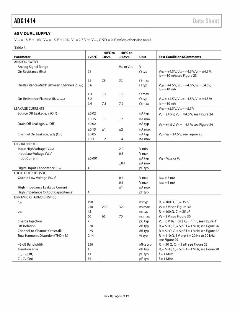
±5 V DUAL SUPPLY VDD = +5 V ± 10%, VSS = −5 V ± 10%, VL = 2.7 V to VDD, GND = 0 V, unless otherwise noted.
Table 3.
Parameter +25°C −40°C to +85°C
−40°C to +125°C Unit Test Conditions/Comments
ANALOG SWITCH Analog Signal Range VSS to VDD V On Resistance (RON) 21 Ω typ VDD = +4.5 V, VSS = −4.5 V, VS = ±4.5 V,
IS = −10 mA; see Figure 23 25 29 32 Ω max On-Resistance Match Between Channels (ΔRON) 0.6 Ω typ VDD = +4.5 V, VSS = −4.5 V, VS = ±4.5V,
IS = −10 mA 1.3 1.7 1.9 Ω max
On-Resistance Flatness (RFLAT (ON)) 5.2 Ω typ VDD = +4.5 V, VSS = −4.5 V, VS = ±4.5 V; 6.4 7.3 7.6 Ω max IS = −10 mA
LEAKAGE CURRENTS VDD = +5.5 V, VSS = −5.5 V Source Off Leakage, IS (Off ) ±0.02 nA typ VS = ±4.5 V, VD = ∓4.5 V; see Figure 24 ±0.15 ±1 ±2 nA max Drain Off Leakage, ID (Off ) ±0.02 nA typ VS = ±4.5 V, VD = ∓4.5 V; see Figure 24
±0.15 ±1 ±2 nA max Channel On Leakage, ID, IS (On) ±0.05 nA typ VS = VD = ±4.5 V; see Figure 25
±0.3 ±2 ±4 nA max DIGITAL INPUTS
Input High Voltage (VINH) 2.0 V min Input Low Voltage (VINL) 0.8 V max Input Current ±0.001 µA typ VIN = VGND or VL ±0.1 µA max Digital Input Capacitance (CIN) 4 pF typ
LOGIC OUTPUTS (SDO) Output Low Voltage (VOL)1 0.4 V max ISINK = 3 mA 0.6 V max ISINK = 6 mA High Impedance Leakage Current ±1 µA max High Impedance Output Capacitance1 4 pF typ
DYNAMIC CHARACTERISTICS1 tON 190 ns typ RL = 100 Ω, CL = 35 pF 250 290 320 ns max VS = 3 V; see Figure 30 tOFF 45 ns typ RL = 100 Ω, CL = 35 pF 60 65 70 ns max VS = 3 V; see Figure 30 Charge Injection 7 pC typ VS = 0 V, RS = 0 Ω, CL = 1 nF; see Figure 31 Off Isolation –70 dB typ RL = 50 Ω, CL = 5 pF, f = 1 MHz; see Figure 26 Channel-to-Channel Crosstalk –75 dB typ RL = 50 Ω, CL = 5 pF, f = 1 MHz; see Figure 27 Total Harmonic Distortion (THD + N) 0.14 % typ RL = 110 Ω, 5 V p-p, f = 20 Hz to 20 kHz;
see Figure 29 −3 dB Bandwidth 256 MHz typ RL = 50 Ω, CL = 5 pF; see Figure 28 Insertion Loss 1 dB typ RL = 50 Ω, CL = 5 pF, f = 1 MHz; see Figure 28 CD, CS (Off ) 11 pF typ f = 1 MHz CD, CS (On) 35 pF typ f = 1 MHz
Data Sheet ADG1414
Rev. B | Page 7 of 19
Parameter +25°C −40°C to +85°C
−40°C to +125°C Unit Test Conditions/Comments
POWER REQUIREMENTS VDD = +5.5 V, VSS = −5.5 V IDD 0.001 µA typ Digital inputs = 0 V or VL 1 µA max IL Inactive 0.3 µA typ Digital inputs = 0 V or VL 1 µA max IL Active at 30 MHz 0.26 mA typ Digital inputs toggle between 0 V and VL 0.3 0.35 mA max IL Active at 50 MHz 0.42 mA typ Digital inputs toggle between 0 V and VL 0.5 0.55 mA max ISS 0.001 µA typ Digital inputs = 0 V or VL 1 µA max VDD/VSS ±4.5/±16.5 V min/max
1 Guaranteed by design, not subject to production test.
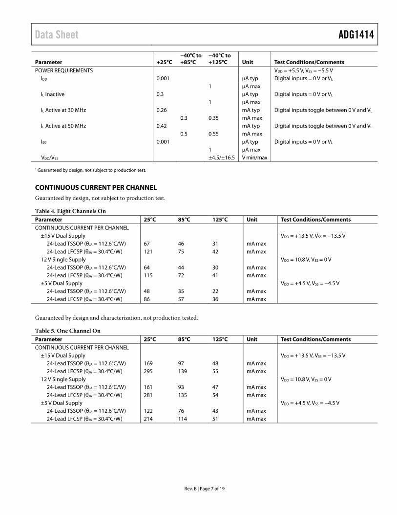
CONTINUOUS CURRENT PER CHANNEL Guaranteed by design, not subject to production test.
Table 4. Eight Channels On Parameter 25°C 85°C 125°C Unit Test Conditions/Comments CONTINUOUS CURRENT PER CHANNEL
±15 V Dual Supply VDD = +13.5 V, VSS = −13.5 V 24-Lead TSSOP (θJA = 112.6°C/W) 67 46 31 mA max 24-Lead LFCSP (θJA = 30.4°C/W) 121 75 42 mA max
12 V Single Supply VDD = 10.8 V, VSS = 0 V 24-Lead TSSOP (θJA = 112.6°C/W) 64 44 30 mA max 24-Lead LFCSP (θJA = 30.4°C/W) 115 72 41 mA max
±5 V Dual Supply VDD = +4.5 V, VSS = −4.5 V 24-Lead TSSOP (θJA = 112.6°C/W) 48 35 22 mA max 24-Lead LFCSP (θJA = 30.4°C/W) 86 57 36 mA max
Guaranteed by design and characterization, not production tested.
Table 5. One Channel On Parameter 25°C 85°C 125°C Unit Test Conditions/Comments CONTINUOUS CURRENT PER CHANNEL
±15 V Dual Supply VDD = +13.5 V, VSS = −13.5 V 24-Lead TSSOP (θJA = 112.6°C/W) 169 97 48 mA max 24-Lead LFCSP (θJA = 30.4°C/W) 295 139 55 mA max
12 V Single Supply VDD = 10.8 V, VSS = 0 V 24-Lead TSSOP (θJA = 112.6°C/W) 161 93 47 mA max 24-Lead LFCSP (θJA = 30.4°C/W) 281 135 54 mA max
±5 V Dual Supply VDD = +4.5 V, VSS = −4.5 V 24-Lead TSSOP (θJA = 112.6°C/W) 122 76 43 mA max 24-Lead LFCSP (θJA = 30.4°C/W) 214 114 51 mA max
ADG1414 Data Sheet
Rev. B | Page 8 of 19
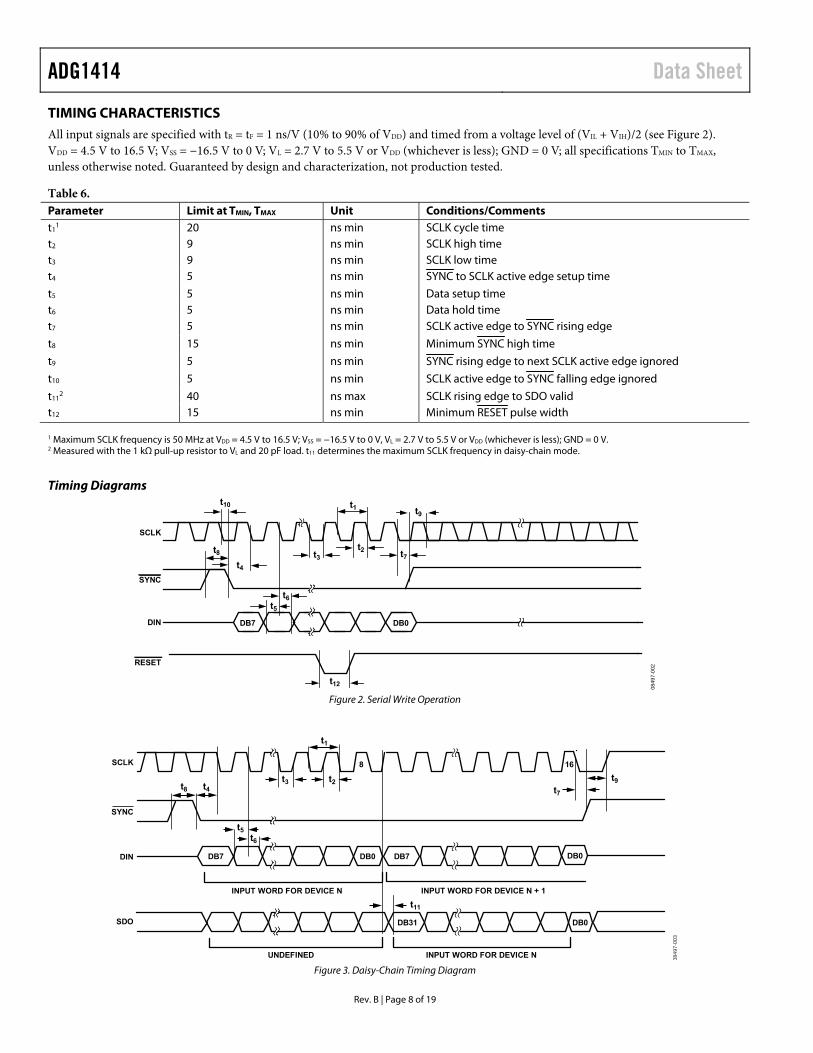
TIMING CHARACTERISTICS All input signals are specified with tR = tF = 1 ns/V (10% to 90% of VDD) and timed from a voltage level of (VIL + VIH)/2 (see Figure 2). VDD = 4.5 V to 16.5 V; VSS = −16.5 V to 0 V; VL = 2.7 V to 5.5 V or VDD (whichever is less); GND = 0 V; all specifications TMIN to TMAX, unless otherwise noted. Guaranteed by design and characterization, not production tested.
Table 6. Parameter Limit at TMIN, TMAX Unit Conditions/Comments t1
1 20 ns min SCLK cycle time t2 9 ns min SCLK high time t3 9 ns min SCLK low time t4 5 ns min SYNC to SCLK active edge setup time
t5 5 ns min Data setup time t6 5 ns min Data hold time t7 5 ns min SCLK active edge to SYNC rising edge
t8 15 ns min Minimum SYNC high time
t9 5 ns min SYNC rising edge to next SCLK active edge ignored
t10 5 ns min SCLK active edge to SYNC falling edge ignored
t112 40 ns max SCLK rising edge to SDO valid
t12 15 ns min Minimum RESET pulse width 1 Maximum SCLK frequency is 50 MHz at VDD = 4.5 V to 16.5 V; VSS = −16.5 V to 0 V, VL = 2.7 V to 5.5 V or VDD (whichever is less); GND = 0 V. 2 Measured with the 1 kΩ pull-up resistor to VL and 20 pF load. t11 determines the maximum SCLK frequency in daisy-chain mode.
Timing Diagrams
t4
t3
SCLK
DIN
t1
t2
t5
t6
t7t8
DB7
t9
t10
SYNC
t12
RESET
DB0
0849
7-0
02
Figure 2. Serial Write Operation
t8 t4
t3
t6
t11
t7
t9
t5
8 16SCLK
SYNC
DIN
SDO
UNDEFINED
INPUT WORD FOR DEVICE N
INPUT WORD FOR DEVICE N
INPUT WORD FOR DEVICE N + 1
t1
t2
DB0DB7 DB0DB7
DB31 DB0
084
97-0
03
Figure 3. Daisy-Chain Timing Diagram
Data Sheet ADG1414
Rev. B | Page 9 of 19
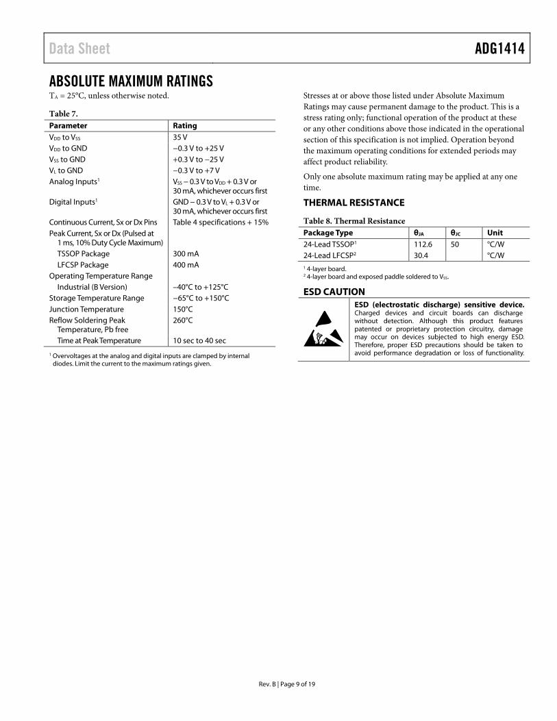
ABSOLUTE MAXIMUM RATINGS TA = 25°C, unless otherwise noted.
Table 7. Parameter Rating VDD to VSS 35 V VDD to GND −0.3 V to +25 V VSS to GND +0.3 V to −25 V VL to GND −0.3 V to +7 V Analog Inputs1 VSS − 0.3 V to VDD + 0.3 V or
30 mA, whichever occurs first Digital Inputs1 GND − 0.3 V to VL + 0.3 V or
30 mA, whichever occurs first Continuous Current, Sx or Dx Pins Table 4 specifications + 15% Peak Current, Sx or Dx (Pulsed at
1 ms, 10% Duty Cycle Maximum)
TSSOP Package 300 mA LFCSP Package 400 mA
Operating Temperature Range Industrial (B Version) –40°C to +125°C
Storage Temperature Range −65°C to +150°C Junction Temperature 150°C Reflow Soldering Peak
Temperature, Pb free 260°C
Time at Peak Temperature 10 sec to 40 sec
1 Overvoltages at the analog and digital inputs are clamped by internal diodes. Limit the current to the maximum ratings given.
Stresses at or above those listed under Absolute Maximum Ratings may cause permanent damage to the product. This is a stress rating only; functional operation of the product at these or any other conditions above those indicated in the operational section of this specification is not implied. Operation beyond the maximum operating conditions for extended periods may affect product reliability.
Only one absolute maximum rating may be applied at any one time.
THERMAL RESISTANCE
Table 8. Thermal Resistance Package Type θJA θJC Unit 24-Lead TSSOP1 112.6 50 °C/W 24-Lead LFCSP2 30.4 °C/W 1 4-layer board. 2 4-layer board and exposed paddle soldered to VSS.
ESD CAUTION
ADG1414 Data Sheet
Rev. B | Page 10 of 19
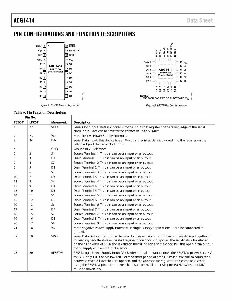
PIN CONFIGURATIONS AND FUNCTION DESCRIPTIONS
1
2
3
4
5
6
7
8
9
10
12
11
VDD
DIN
GND
S2
D1
S1
SCLK
D2
S3
D4
S4
D3
20
21
22
23
24
19
18
17
16
15
14
13
RESET/VL
SDO
VSS
S7
D8
S8
D7
S6
D5
S5
D6
SYNC
ADG1414TOP VIEW
(Not to Scale)
084
97-0
04
Figure 4. TSSOP Pin Configuration
GND
S1
D1
S2
D2
S3
S7
D8
S8
VSS
D7
S6
D3
S4
D4
S5
D6
D5
SY
NC
SC
LK
VD
D
DIN
RE
SE
T/V
L
SD
O
084
97-0
05
2
1
3
4
5
6
18
17
16
15
14
13
8 9 10 117 12
20 1921222324
NOTES1. EXPOSED PAD TIED TO SUBSTRATE, VSS.
ADG1414TOP VIEW
(Not to Scale)
Figure 5. LFCSP Pin Configuration
Table 9. Pin Function Descriptions Pin No.
Mnemonic Description TSSOP LFCSP 1 22 SCLK Serial Clock Input. Data is clocked into the input shift register on the falling edge of the serial
clock input. Data can be transferred at rates of up to 50 MHz. 2 23 VDD Most Positive Power Supply Potential. 3 24 DIN Serial Data Input. This device has an 8-bit shift register. Data is clocked into the register on the
falling edge of the serial clock input. 4 1 GND Ground (0 V) Reference. 5 2 S1 Source Terminal 1. This pin can be an input or an output. 6 3 D1 Drain Terminal 1. This pin can be an input or an output. 7 4 S2 Source Terminal 2. This pin can be an input or an output. 8 5 D2 Drain Terminal 2. This pin can be an input or an output. 9 6 S3 Source Terminal 3. This pin can be an input or an output. 10 7 D3 Drain Terminal 3. This pin can be an input or an output. 11 8 S4 Source Terminal 4. This pin can be an input or an output. 12 9 D4 Drain Terminal 4. This pin can be an input or an output. 13 10 D5 Drain Terminal 5. This pin can be an input or an output. 14 11 S5 Source Terminal 5. This pin can be an input or an output. 15 12 D6 Drain Terminal 6. This pin can be an input or an output. 16 13 S6 Source Terminal 6. This pin can be an input or an output. 17 14 D7 Drain Terminal 7. This pin can be an input or an output. 18 15 S7 Source Terminal 7. This pin can be an input or an output. 19 16 D8 Drain Terminal 8. This pin can be an input or an output. 20 17 S8 Source Terminal 8. This pin can be an input or an output. 21 18 VSS Most Negative Power Supply Potential. In single-supply applications, it can be connected to
ground. 22 19 SDO Serial Data Output. This pin can be used for daisy-chaining a number of these devices together or
for reading back the data in the shift register for diagnostic purposes. The serial data is transferred on the rising edge of SCLK and is valid on the falling edge of the clock. Pull this open-drain output to the supply with an external resistor.
23 20 RESET/VL RESET/Logic Power Supply Input (VL). Under normal operation, drive the RESET/VL pin with a 2.7 V to 5 V supply. Pull the pin low (<0.8 V) for a short period of time (15 ns is sufficient) to complete a hardware reset. All switches are opened, and the appropriate registers are cleared to 0. When using the RESET/VL pin to complete a hardware reset, all other SPI pins (SYNC, SCLK, and DIN) must be driven low.
Data Sheet ADG1414
Rev. B | Page 11 of 19
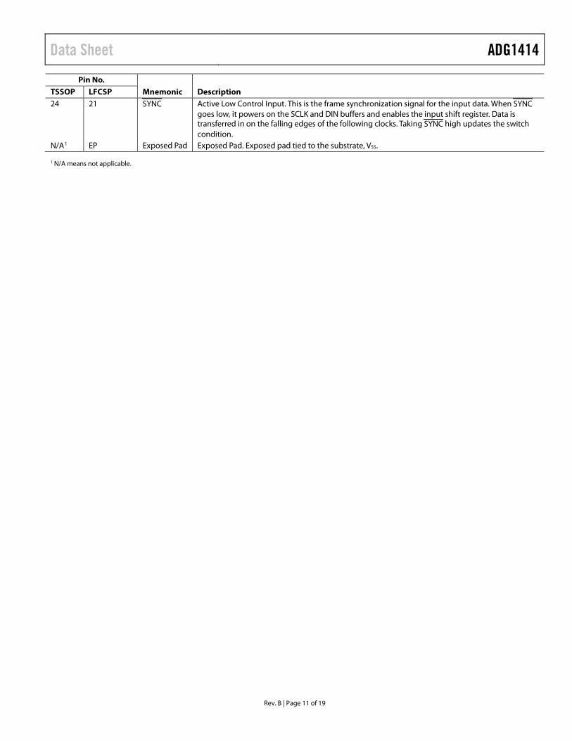
Pin No. Mnemonic Description TSSOP LFCSP
24 21 SYNC Active Low Control Input. This is the frame synchronization signal for the input data. When SYNC goes low, it powers on the SCLK and DIN buffers and enables the input shift register. Data is transferred in on the falling edges of the following clocks. Taking SYNC high updates the switch condition.
N/A1 EP Exposed Pad Exposed Pad. Exposed pad tied to the substrate, VSS. 1 N/A means not applicable.
ADG1414 Data Sheet
Rev. B | Page 12 of 19
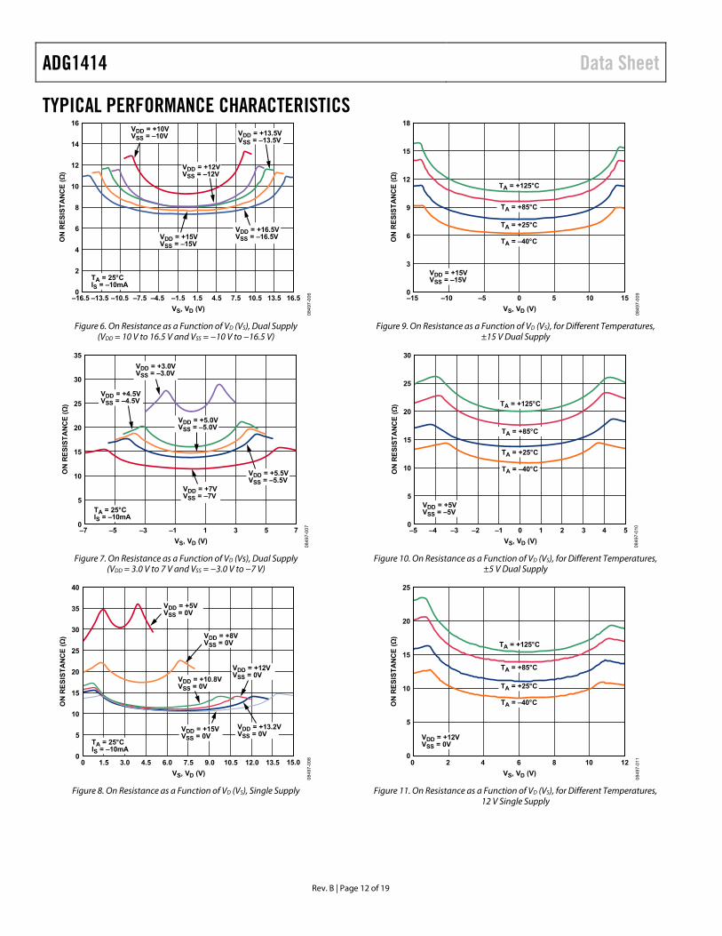
TYPICAL PERFORMANCE CHARACTERISTICS 16
14
12
10
8
6
4
2
0–16.5 –13.5 –4.5 4.5 16.5
ON
RES
ISTA
NC
E (Ω
)
VS, VD (V)–10.5 –1.5 7.5–7.5 1.5 10.5 13.5
VDD = +10VVSS = –10V
VDD = +15VVSS = –15V
VDD = +12VVSS = –12V
VDD = +13.5VVSS = –13.5V
VDD = +16.5VVSS = –16.5V
TA = 25°CIS = –10mA
0849
7-00
6
Figure 6. On Resistance as a Function of VD (VS), Dual Supply (VDD = 10 V to 16.5 V and VSS = −10 V to −16.5 V)
35
30
25
20
15
10
5
0–7 –1 7
ON
RES
ISTA
NC
E (Ω
)
VS, VD (V)–5 1–3 3 5
VDD = +3.0VVSS = –3.0V
VDD = +7VVSS = –7V
VDD = +4.5VVSS = –4.5V
VDD = +5.5VVSS = –5.5V
VDD = +5.0VVSS = –5.0V
TA = 25°CIS = –10mA
0849
7-00
7
Figure 7. On Resistance as a Function of VD (Vs), Dual Supply
(VDD = 3.0 V to 7 V and VSS = −3.0 V to −7 V)
40
35
30
25
20
15
10
5
01.50
ON
RES
ISTA
NC
E (Ω
)
VS, VD (V)3.0 4.5 6.0 7.5 9.0 10.5 12.0 13.5 15.0
VDD = +5VVSS = 0V
VDD = +8VVSS = 0V
VDD = +10.8VVSS = 0V
TA = 25°CIS = –10mA
VDD = +12VVSS = 0V
VDD = +13.2VVSS = 0VVDD = +15V
VSS = 0V
0849
7-00
8
Figure 8. On Resistance as a Function of VD (VS), Single Supply
18
15
12
9
6
3
0–15 –10 –5 0 5 10 15
ON
RES
ISTA
NC
E (Ω
)
VS, VD (V)
VDD = +15VVSS = –15V
TA = +125°C
TA = +85°C
TA = +25°C
TA = –40°C
0849
7-00
9
Figure 9. On Resistance as a Function of VD (VS), for Different Temperatures,
±15 V Dual Supply
30
25
20
15
10
5
0–5 –3–4 –2 0–1 321 4 5
ON
RES
ISTA
NC
E (Ω
)
VS, VD (V)
VDD = +5VVSS = –5V
TA = +125°C
TA = +85°C
TA = +25°C
TA = –40°C
0849
7-01
0
Figure 10. On Resistance as a Function of VD (VS), for Different Temperatures,
±5 V Dual Supply
25
20
15
10
5
00 12108642
ON
RES
ISTA
NC
E (Ω
)
VS, VD (V)
VDD = +12VVSS = 0V
TA = +125°C
TA = +85°C
TA = +25°C
TA = –40°C
0849
7-01
1
Figure 11. On Resistance as a Function of VD (VS), for Different Temperatures,
12 V Single Supply
Data Sheet ADG1414
Rev. B | Page 13 of 19
2.5
–2.0
–1.5
–1.0
–0.5
0
0.5
1.0
1.5
2.0
0 12010080604020
LEA
KA
GE
CU
RR
ENT
(nA
)
TEMPERATURE (°C)
VDD = +15VVSS = –15VVBIAS = +10/–10V ID, IS (ON) – –
ID, IS (ON) ++
ID (OFF) –+
IS (OFF) –+
ID (OFF) +–
IS (OFF) +–
0849
7-01
3
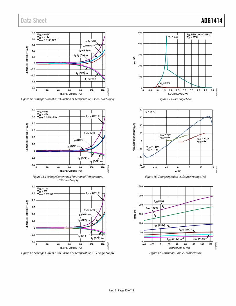
Figure 12. Leakage Current as a Function of Temperature, ±15 V Dual Supply
3.0
2.5
–1.0
–0.5
0
0.5
1.0
1.5
2.0
0 12010080604020
LEA
KA
GE
CU
RR
ENT
(nA
)
TEMPERATURE (°C)
VDD = +5VVSS = –5VVBIAS = +4.5/–4.5V
ID, IS (ON) – –
ID, IS (ON) ++
ID (OFF) –+
ID (OFF) +–
IS (OFF) +–
IS (OFF) –+
0849
7-01
4
Figure 13. Leakage Current as a Function of Temperature, ±5 V Dual Supply
3.0
2.5
–1.0
–0.5
0
0.5
1.0
1.5
2.0
0 12010080604020
LEA
KA
GE
CU
RR
ENT
(nA
)
TEMPERATURE (°C)
VDD = 12VVSS = 0VVBIAS = 1V/10V
ID, IS (ON) – –
ID, IS (ON) ++
ID (OFF) –+
IS (OFF) +–
ID (OFF) +–IS (OFF) –+
0849
7-01
5
Figure 14. Leakage Current as a Function of Temperature, 12 V Single Supply
500
400
300
200
100
00 5.04.54.03.53.02.52.01.51.00.5
I DD
(µA
)
LOGIC LEVEL (V)
IDD PER LOGIC INPUTTA = 25°CVL = 5.5V
VL = 2.7V
0849
7-01
6
Figure 15. IDD vs. Logic Level
80
–60
–40
–20
0
20
40
60
–15 –10 –5 0 5 10 15
CH
AR
GE
INJE
CTI
ON
(pC
)
VS (V)
TA = 25°C
VDD = +12VVSS = 0V
VDD = +5VVSS = –5V
VDD = +15VVSS = –15V
0849
7-01
7
Figure 16. Charge Injection vs. Source Voltage (VS)
300
250
200
150
100
50
0–40 1201008060400 20–20
TIM
E (n
s)
TEMPERATURE (°C)
tON (±5V)
tON (±15V)
tOFF (±5V)
tOFF (+12V)
tON (+12V)
tOFF (±15V)
0849
7-01
8
Figure 17. Transition Time vs. Temperature
ADG1414 Data Sheet
Rev. B | Page 14 of 19
0
–120
–100
–80
–60
–40
–20
1k 10k 100k 1M 10M 100M 1G
OF
F I
SO
LA
TIO
N (
dB
)
FREQUENCY (Hz)
TA = 25°CVDD = +15VVSS = –15V
084
97-0
19
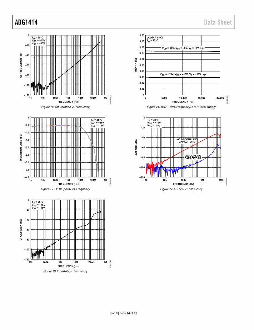
Figure 18. Off Isolation vs. Frequency
0
–4.0
–3.5
–3.0
–2.5
–2.0
–1.5
–1.0
–0.5
1k 10k 100k 1M 10M 100M 1G
INS
ER
TIO
N L
OS
S (
dB
)
FREQUENCY (Hz)
TA = 25°CVDD = +15VVSS = –15V
084
97-0
12
Figure 19. On Response vs. Frequency
0
–120
–100
–80
–60
–40
–20
10k 100k 1M 10M 100M 1G
CR
OS
ST
AL
K (
dB
)
FREQUENCY (Hz)
TA = 25°CVDD = +15VVSS = –15V
084
97-0
21
Figure 20. Crosstalk vs. Frequency
0.20
0
0.02
0.04
0.06
0.08
0.10
0.12
0.14
0.16
0.18
0 5000 10,000 15,000 20,000
TH
D +
N (
%)
FREQUENCY (Hz)
LOAD = 110ΩTA = 25°C
VDD = +5V, VSS = –5V, VS = +5V p-p
VDD = +15V, VSS = –15V, VS = +10V p-p
084
97-0
23
Figure 21. THD + N vs. Frequency, ±15 V Dual Supply
0
–120
–100
–80
–60
–40
–20
1k 10k 100k 1M 10M
AC
PS
RR
(d
B)
FREQUENCY (Hz)
TA = 25°CVDD = +15VVSS = –15V
NO DECOUPLINGCAPACITORS
DECOUPLINGCAPACITORS
084
97-0
25
Figure 22. ACPSRR vs. Frequency

Data Sheet ADG1414
Rev. B | Page 15 of 19
TEST CIRCUITS IDS
V1
S D
VS RON = V1/IDS
084
97-0
26
Figure 23. On Resistance
S D
VS VD
IS (OFF) ID (OFF)
A A0
8497
-027
Figure 24. Off Leakage
S D
VD
ID (ON)
ANC
NC = NO CONNECT
084
97-0
28
Figure 25. On Leakage
VOUTRL50Ω
IN
GND
VIN
S
D
VDD VSS
VDD VSS
50Ω
NETWORKANALYZER
OFF ISOLATION = 20 logVOUT
VS
0.1µF0.1µF
50Ω
VS
084
97-0
32
Figure 26. Off Isolation
CHANNEL-TO-CHANNEL CROSSTALK = 20 logVOUT
VS
GND
S1
D
S2
VOUT
NETWORKANALYZER
RL50Ω
R50Ω
VS
VDD VSS
0.1µF
VDD
0.1µF
VSS
084
97-0
33
Figure 27. Channel-to-Channel Crosstalk
VOUTRL50Ω
IN
GND
VIN
S
D
VDD VSS
VDD VSS
NETWORKANALYZER
INSERTION LOSS = 20 logVOUT WITH SWITCH
VOUT WITHOUT SWITCH
0.1µF0.1µF
50Ω
VS
084
97-
034
Figure 28. Insertion Loss
VOUT
RS
AUDIO PRECISION
RL10kΩ
IN
VIN
S
D
VSV p-p
VDD VSS
0.1µF
VDD
0.1µF
VSS
GND
084
97-0
35
Figure 29. THD + Noise
ADG1414 Data Sheet
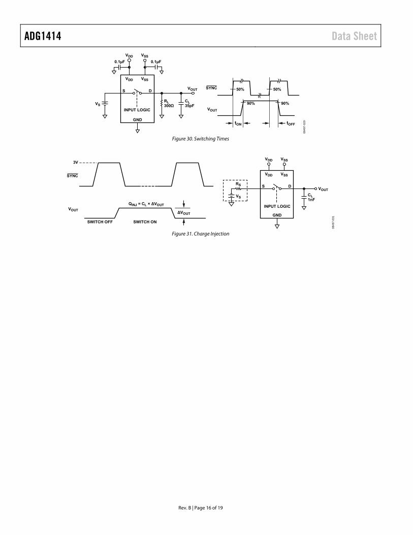
Rev. B | Page 16 of 19
VDD VSS
VDD VSS
0.1µF 0.1µF
GND
RL300Ω
CL35pFVS
INPUT LOGIC
S DVOUT SYNC
VOUT
50% 50%
90% 90%
tON tOFF
084
97-0
29
Figure 30. Switching Times
VDD VSS
VDD VSS
GND
INPUT LOGIC
CL1nF
S DVOUT
RS
VS
SYNC
3V
VOUT∆VOUT
QINJ = CL × ∆VOUT
SWITCH OFF SWITCH ON
084
97-0
31
Figure 31. Charge Injection
Data Sheet ADG1414
Rev. B | Page 17 of 19
TERMINOLOGY IDD The positive supply current.
ISS The negative supply current.
VD (VS) The analog voltage on Terminal Dx or Terminal Sx.
RON The ohmic resistance between Terminal Dx and Terminal Sx.
ΔRON The difference between the RON of any two channels.
RFLAT (ON) Flatness is defined as the difference between the maximum and minimum value of on resistance, as measured over the specified analog signal range.
IS (Off) The source leakage current with the switch off.
ID (Off) The drain leakage current with the switch off.
ID, IS (On) The channel leakage current with the switch on.
VINL The maximum input voltage for Logic 0.
VINH The minimum input voltage for Logic 1.
IINL (IINH) The input current of the digital input.
CS (Off) The off switch source capacitance, measured with reference to ground.
CD (Off) The off switch drain capacitance, measured with reference to ground.
CD, CS (On) The on switch capacitance, measured with reference to ground.
CIN The digital input capacitance.
tON The delay between applying the digital control input and the output switching on. See Figure 30.
tOFF The delay between applying the digital control input and the output switching off. See Figure 30.
Charge Injection A measure of the glitch impulse transferred from the digital input to the analog output during switching.
Off Isolation A measure of unwanted signal coupling through an off switch.
Crosstalk A measure of unwanted signal that is coupled through from one channel to another as a result of parasitic capacitance.
Bandwidth The frequency at which the output is attenuated by 3 dB.
On Response The frequency response of the on switch.
Insertion Loss The loss due to the on resistance of the switch.
THD + N The ratio of the harmonic amplitude plus noise of the signal to the fundamental.
AC Power Supply Rejection Ratio (ACPSRR) A measure of the ability of a device to avoid coupling noise and spurious signals that appear on the supply voltage pin to the output of the switch. The dc voltage on the device is modulated by a sine wave of 0.62 V p-p. The ratio of the amplitude of signal on the output to the amplitude of the modulation is the ACPSRR.
ADG1414 Data Sheet
Rev. B | Page 18 of 19
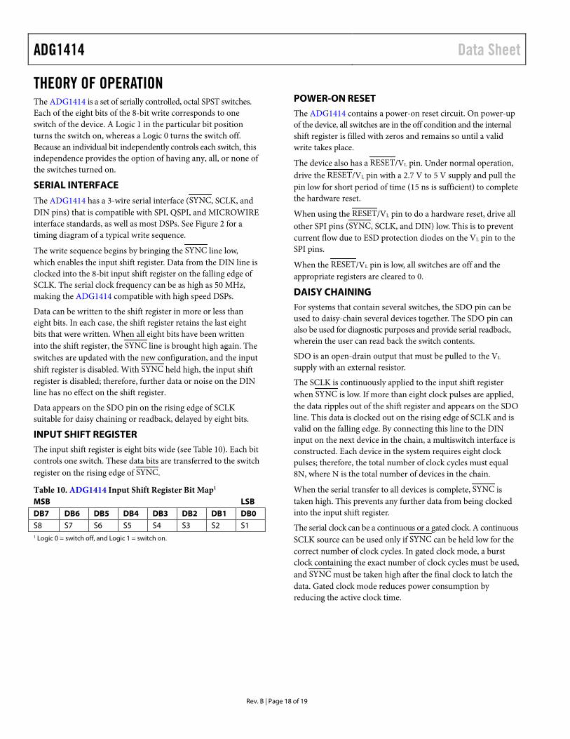
THEORY OF OPERATION The ADG1414 is a set of serially controlled, octal SPST switches. Each of the eight bits of the 8-bit write corresponds to one switch of the device. A Logic 1 in the particular bit position turns the switch on, whereas a Logic 0 turns the switch off. Because an individual bit independently controls each switch, this independence provides the option of having any, all, or none of the switches turned on.
SERIAL INTERFACE
The ADG1414 has a 3-wire serial interface (SYNC, SCLK, and DIN pins) that is compatible with SPI, QSPI, and MICROWIRE interface standards, as well as most DSPs. See Figure 2 for a timing diagram of a typical write sequence.
The write sequence begins by bringing the SYNC line low, which enables the input shift register. Data from the DIN line is clocked into the 8-bit input shift register on the falling edge of SCLK. The serial clock frequency can be as high as 50 MHz, making the ADG1414 compatible with high speed DSPs.
Data can be written to the shift register in more or less than eight bits. In each case, the shift register retains the last eight bits that were written. When all eight bits have been written into the shift register, the SYNC line is brought high again. The switches are updated with the new configuration, and the input shift register is disabled. With SYNC held high, the input shift register is disabled; therefore, further data or noise on the DIN line has no effect on the shift register.
Data appears on the SDO pin on the rising edge of SCLK suitable for daisy chaining or readback, delayed by eight bits.
INPUT SHIFT REGISTER The input shift register is eight bits wide (see Table 10). Each bit controls one switch. These data bits are transferred to the switch register on the rising edge of SYNC.
Table 10. ADG1414 Input Shift Register Bit Map1 MSB LSB DB7 DB6 DB5 DB4 DB3 DB2 DB1 DB0 S8 S7 S6 S5 S4 S3 S2 S1 1 Logic 0 = switch off, and Logic 1 = switch on.
POWER-ON RESET The ADG1414 contains a power-on reset circuit. On power-up of the device, all switches are in the off condition and the internal shift register is filled with zeros and remains so until a valid write takes place.
The device also has a RESET/VL pin. Under normal operation, drive the RESET/VL pin with a 2.7 V to 5 V supply and pull the pin low for short period of time (15 ns is sufficient) to complete the hardware reset.
When using the RESET/VL pin to do a hardware reset, drive all other SPI pins (SYNC, SCLK, and DIN) low. This is to prevent current flow due to ESD protection diodes on the VL pin to the SPI pins.
When the RESET/VL pin is low, all switches are off and the appropriate registers are cleared to 0.
DAISY CHAINING For systems that contain several switches, the SDO pin can be used to daisy-chain several devices together. The SDO pin can also be used for diagnostic purposes and provide serial readback, wherein the user can read back the switch contents.
SDO is an open-drain output that must be pulled to the VL supply with an external resistor.
The SCLK is continuously applied to the input shift register when SYNC is low. If more than eight clock pulses are applied, the data ripples out of the shift register and appears on the SDO line. This data is clocked out on the rising edge of SCLK and is valid on the falling edge. By connecting this line to the DIN input on the next device in the chain, a multiswitch interface is constructed. Each device in the system requires eight clock pulses; therefore, the total number of clock cycles must equal 8N, where N is the total number of devices in the chain.
When the serial transfer to all devices is complete, SYNC is taken high. This prevents any further data from being clocked into the input shift register.
The serial clock can be a continuous or a gated clock. A continuous SCLK source can be used only if SYNC can be held low for the correct number of clock cycles. In gated clock mode, a burst clock containing the exact number of clock cycles must be used, and SYNC must be taken high after the final clock to latch the data. Gated clock mode reduces power consumption by reducing the active clock time.
Data Sheet ADG1414
Rev. B | Page 19 of 19
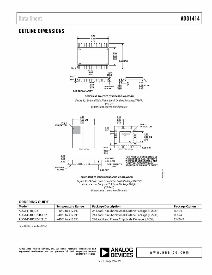
OUTLINE DIMENSIONS
24 13
1216.40 BSC
4.504.404.30
PIN 1
7.907.807.70
0.150.05
0.300.19
0.65BSC
1.20MAX
0.200.09
0.750.600.45
8°0°
SEATINGPLANE
0.10 COPLANARITY
COMPLIANT TO JEDEC STANDARDS MO-153-AD Figure 32. 24-Lead Thin Shrink Small Outline Package [TSSOP]
(RU-24) Dimensions shown in millimeters
0.50BSC
0.500.400.30
0.300.250.18
COMPLIANT TO JEDEC STANDARDS MO-220-WGGD. 03-
11-
20
13-A
BOTTOM VIEWTOP VIEW
EXPOSEDPAD
PIN 1INDICATOR
4.104.00 SQ3.90
SEATINGPLANE
0.800.750.70
0.20 REF
0.25 MIN
COPLANARITY0.08
PIN 1INDICATOR
2.652.50 SQ2.45
1
24
712
13
18
19
6
0.05 MAX0.02 NOM
FOR PROPER CONNECTION OFTHE EXPOSED PAD, REFER TOTHE PIN CONFIGURATION ANDFUNCTION DESCRIPTIONSSECTION OF THIS DATA SHEET.
Figure 33. 24-Lead Lead Frame Chip Scale Package [LFCSP]
4 mm × 4 mm Body and 0.75 mm Package Height (CP-24-7)
Dimensions shown in millimeters
ORDERING GUIDE Model1 Temperature Range Package Description Package Option ADG1414BRUZ −40°C to +125°C 24-Lead Thin Shrink Small Outline Package [TSSOP] RU-24 ADG1414BRUZ-REEL7 −40°C to +125°C 24-Lead Thin Shrink Small Outline Package [TSSOP] RU-24 ADG1414BCPZ-REEL7 −40°C to +125°C 24-Lead Lead Frame Chip Scale Package [LFCSP] CP-24-7 1 Z = RoHS Compliant Part.
©2009–2015 Analog Devices, Inc. All rights reserved. Trademarks and registered trademarks are the property of their respective owners. D08497-0-11/15(B)