1.5 Ω on resistance, ±15 v/+12 v/±5 v, icmos, quad spst ... · v max . input current, i inl or i...
TRANSCRIPT
1.5 Ω On Resistance, ±15 V/+12 V/±5 V, iCMOS, Quad SPST Switches
Data Sheet ADG1411/ADG1412/ADG1413
Rev. C Document Feedback Information furnished by Analog Devices is believed to be accurate and reliable. However, no responsibility is assumed by Analog Devices for its use, nor for any infringements of patents or other rights of third parties that may result from its use. Specifications subject to change without notice. No license is granted by implication or otherwise under any patent or patent rights of Analog Devices. Trademarks and registered trademarks are the property of their respective owners.
One Technology Way, P.O. Box 9106, Norwood, MA 02062-9106, U.S.A.Tel: 781.329.4700 ©2008–2016 Analog Devices, Inc. All rights reserved. Technical Support www.analog.com
FEATURES 1.5 Ω on resistance 0.3 Ω on-resistance flatness 0.1 Ω on-resistance match between channels Continuous current per channel
LFCSP: 250 mA TSSOP: 190 mA
Fully specified at +12 V, ±15 V, and ±5 V No VL supply required 3 V logic-compatible inputs Rail-to-rail operation 16-lead TSSOP and 16-lead, 4 mm × 4 mm LFCSP Qualified for automotive applications
APPLICATIONS Automated test equipment Data acquisition systems Battery-powered systems Sample-and-hold systems Audio signal routing Video signal routing Communications systems Relay replacement
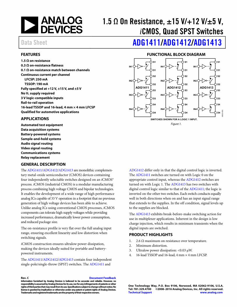
FUNCTIONAL BLOCK DIAGRAM
IN1
S1
D1
IN2
S2
D2
IN3
S3
D3
IN4
S4
D4
ADG1411
IN1
S1
D1
IN2
S2
D2
IN3
S3
D3
IN4
S4
D4
ADG1412
SWITCHES SHOWN FOR A LOGIC 1 INPUT.
IN2
S2
D2
IN3
S3
D3
IN1
S1
D1
IN4
S4
D4
ADG1413
0681
5-00
1
Figure 1.
GENERAL DESCRIPTION The ADG1411/ADG1412/ADG1413 are monolithic complemen-tary metal-oxide semiconductor (CMOS) devices containing four independently selectable switches designed on an iCMOS® process. iCMOS (industrial CMOS) is a modular manufacturing process combining high voltage CMOS and bipolar technologies. It enables the development of a wide range of high performance analog ICs capable of 33 V operation in a footprint that no previous generation of high voltage devices has been able to achieve. Unlike analog ICs using conventional CMOS processes, iCMOS components can tolerate high supply voltages while providing increased performance, dramatically lower power consumption, and reduced package size.
The on-resistance profile is very flat over the full analog input range, ensuring excellent linearity and low distortion when switching signals.
iCMOS construction ensures ultralow power dissipation, making the devices ideally suited for portable and battery-powered instruments.
The ADG1411/ADG1412/ADG1413 contain four independent single-pole/single-throw (SPST) switches. The ADG1411 and
ADG1412 differ only in that the digital control logic is inverted. The ADG1411 switches are turned on with Logic 0 on the appropriate control input, whereas the ADG1412 switches are turned on with Logic 1. The ADG1413 has two switches with digital control logic similar to that of the ADG1411; the logic is inverted on the other two switches. Each switch conducts equally well in both directions when on and has an input signal range that extends to the supplies. In the off condition, signal levels up to the supplies are blocked.
The ADG1413 exhibits break-before-make switching action for use in multiplexer applications. Inherent in the design is low charge injection, which results in minimum transients when the digital inputs are switched.
PRODUCT HIGHLIGHTS 1. 2.6 Ω maximum on resistance over temperature. 2. Minimum distortion. 3. Ultralow power dissipation: <0.03 μW. 4. 16-lead TSSOP and 16-lead, 4 mm × 4 mm LFCSP.
ADG1411/ADG1412/ADG1413 Data Sheet
Rev. C | Page 2 of 16
TABLE OF CONTENTS Features .............................................................................................. 1 Applications ....................................................................................... 1 Functional Block Diagram .............................................................. 1 General Description ......................................................................... 1 Product Highlights ........................................................................... 1 Revision History ............................................................................... 2 Specifications ..................................................................................... 3
±15 V Dual Supply ....................................................................... 3 +12 V Single Supply ..................................................................... 4 ±5 V Dual Supply ......................................................................... 5
Absolute Maximum Ratings ............................................................6 ESD Caution...................................................................................6
Pin Configurations and Function Descriptions ............................7 Typical Performance Characteristics ..............................................8 Terminology .................................................................................... 12 Test Circuits ..................................................................................... 13 Outline Dimensions ....................................................................... 15
Ordering Guide .......................................................................... 16 Automotive Products ................................................................. 16
REVISION HISTORY3/16—Rev. B to Rev. C Changed CP-16-13 to CP-16-26 .................................. Throughout Changes to Figure 2, Figure 3, and Table 5 ................................... 7 Updated Outline Dimensions ....................................................... 15 Changes to Ordering Guide .......................................................... 16 3/11—Rev. A to Rev. B Changes to Features Section............................................................ 1 Changes to Table 5, Added Exposed Pad Notation ...................... 3 Updated Outline Dimensions ....................................................... 15 Changes to Ordering Guide .......................................................... 40 Added Automotive Products Section........................................... 40
3/09—Rev. 0 to Rev. A
Changes to Power Requirements, IDD, Digital Inputs = 5 V Parameter, Table 1 ............................................................................. 3 Changes to Power Requirements, IDD, Digital Inputs = 5 V Parameter Table 2 .............................................................................. 4 5/08—Revision 0: Initial Version
Data Sheet ADG1411/ADG1412/ADG1413
Rev. C | Page 3 of 16
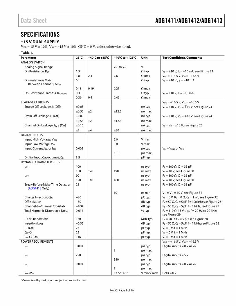
SPECIFICATIONS ±15 V DUAL SUPPLY VDD = 15 V ± 10%, VSS = −15 V ± 10%, GND = 0 V, unless otherwise noted.
Table 1. Parameter 25°C −40°C to +85°C −40°C to +125°C Unit Test Conditions/Comments ANALOG SWITCH
Analog Signal Range VDD to VSS V On Resistance, RON 1.5 Ω typ VS = ±10 V, IS = −10 mA; see Figure 23 1.8 2.3 2.6 Ω max VDD = +13.5 V, VSS = −13.5 V On-Resistance Match
Between Channels, ∆RON 0.1 Ω typ VS = ±10 V , IS = −10 mA
0.18 0.19 0.21 Ω max On-Resistance Flatness, RFLAT(ON) 0.3 Ω typ VS = ±10 V, IS = −10 mA 0.36 0.4 0.45 Ω max
LEAKAGE CURRENTS VDD = +16.5 V, VSS = −16.5 V Source Off Leakage, IS (Off) ±0.03 nA typ VS = ±10 V, VD = ∓10 V; see Figure 24 ±0.55 ±2 ±12.5 nA max Drain Off Leakage, ID (Off) ±0.03 nA typ VS = ±10 V, VD = ∓10 V; see Figure 24
±0.55 ±2 ±12.5 nA max Channel On Leakage, ID, IS (On) ±0.15 nA typ VS = VD = ±10 V; see Figure 25
±2 ±4 ±30 nA max
DIGITAL INPUTS Input High Voltage, VINH 2.0 V min Input Low Voltage, VINL 0.8 V max Input Current, IINL or IINH 0.005 µA typ VIN = VGND or VDD ±0.1 µA max Digital Input Capacitance, CIN 3.5 pF typ
DYNAMIC CHARACTERISTICS1 tON 100 ns typ RL = 300 Ω, CL = 35 pF 150 170 190 ns max VS = 10 V; see Figure 30 tOFF 90 ns typ RL = 300 Ω, CL = 35 pF 120 140 160 ns max VS = 10 V; see Figure 30 Break-Before-Make Time Delay, tD
(ADG1413 Only) 25 ns typ RL = 300 Ω, CL = 35 pF
10 ns min VS1 = VS2 = 10 V; see Figure 31 Charge Injection, QINJ −20 pC typ VS = 0 V, RS = 0 Ω, CL = 1 nF; see Figure 32 Off Isolation −80 dB typ RL = 50 Ω, CL = 5 pF, f = 100 kHz; see Figure 26 Channel-to-Channel Crosstalk −100 dB typ RL = 50 Ω, CL = 5 pF, f = 1 MHz; see Figure 27 Total Harmonic Distortion + Noise 0.014 % typ RL = 110 Ω, 15 V p-p, f = 20 Hz to 20 kHz;
see Figure 29 −3 dB Bandwidth 170 MHz typ RL = 50 Ω, CL = 5 pF; see Figure 28 Insertion Loss −0.35 dB typ RL = 50 Ω, CL = 5 pF, f = 1 MHz; see Figure 28 CS (Off) 23 pF typ VS = 0 V, f = 1 MHz CD (Off) 23 pF typ VS = 0 V, f = 1 MHz CD, CS (On) 116 pF typ VS = 0 V, f = 1 MHz
POWER REQUIREMENTS VDD = +16.5 V, VSS = −16.5 V IDD 0.001 µA typ Digital inputs = 0 V or VDD
1 µA max IDD 220 µA typ Digital inputs = 5 V
380 µA max ISS 0.001 µA typ Digital inputs = 0 V or VDD
1 µA max VDD/VSS ±4.5/±16.5 V min/V max GND = 0 V
1 Guaranteed by design; not subject to production test.
ADG1411/ADG1412/ADG1413 Data Sheet
Rev. C | Page 4 of 16
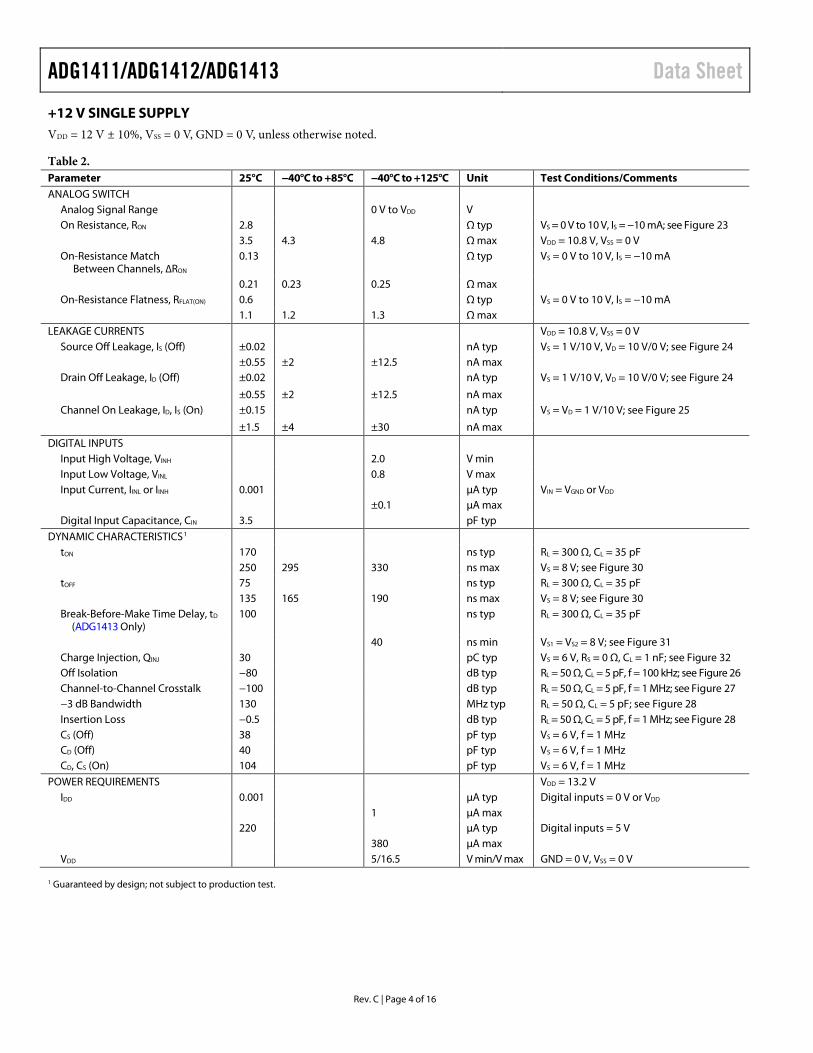
+12 V SINGLE SUPPLY VDD = 12 V ± 10%, VSS = 0 V, GND = 0 V, unless otherwise noted.
Table 2. Parameter 25°C −40°C to +85°C −40°C to +125°C Unit Test Conditions/Comments ANALOG SWITCH
Analog Signal Range 0 V to VDD V On Resistance, RON 2.8 Ω typ VS = 0 V to 10 V, IS = −10 mA; see Figure 23 3.5 4.3 4.8 Ω max VDD = 10.8 V, VSS = 0 V On-Resistance Match
Between Channels, ∆RON 0.13 Ω typ VS = 0 V to 10 V, IS = −10 mA
0.21 0.23 0.25 Ω max On-Resistance Flatness, RFLAT(ON) 0.6 Ω typ VS = 0 V to 10 V, IS = −10 mA 1.1 1.2 1.3 Ω max
LEAKAGE CURRENTS VDD = 10.8 V, VSS = 0 V Source Off Leakage, IS (Off) ±0.02 nA typ VS = 1 V/10 V, VD = 10 V/0 V; see Figure 24 ±0.55 ±2 ±12.5 nA max Drain Off Leakage, ID (Off) ±0.02 nA typ VS = 1 V/10 V, VD = 10 V/0 V; see Figure 24
±0.55 ±2 ±12.5 nA max Channel On Leakage, ID, IS (On) ±0.15 nA typ VS = VD = 1 V/10 V; see Figure 25
±1.5 ±4 ±30 nA max
DIGITAL INPUTS Input High Voltage, VINH 2.0 V min Input Low Voltage, VINL 0.8 V max Input Current, IINL or IINH 0.001 µA typ VIN = VGND or VDD ±0.1 µA max Digital Input Capacitance, CIN 3.5 pF typ
DYNAMIC CHARACTERISTICS1 tON 170 ns typ RL = 300 Ω, CL = 35 pF 250 295 330 ns max VS = 8 V; see Figure 30 tOFF 75 ns typ RL = 300 Ω, CL = 35 pF 135 165 190 ns max VS = 8 V; see Figure 30 Break-Before-Make Time Delay, tD
(ADG1413 Only) 100 ns typ RL = 300 Ω, CL = 35 pF
40 ns min VS1 = VS2 = 8 V; see Figure 31 Charge Injection, QINJ 30 pC typ VS = 6 V, RS = 0 Ω, CL = 1 nF; see Figure 32 Off Isolation −80 dB typ RL = 50 Ω, CL = 5 pF, f = 100 kHz; see Figure 26 Channel-to-Channel Crosstalk −100 dB typ RL = 50 Ω, CL = 5 pF, f = 1 MHz; see Figure 27 −3 dB Bandwidth 130 MHz typ RL = 50 Ω, CL = 5 pF; see Figure 28 Insertion Loss −0.5 dB typ RL = 50 Ω, CL = 5 pF, f = 1 MHz; see Figure 28 CS (Off) 38 pF typ VS = 6 V, f = 1 MHz CD (Off) 40 pF typ VS = 6 V, f = 1 MHz CD, CS (On) 104 pF typ VS = 6 V, f = 1 MHz
POWER REQUIREMENTS VDD = 13.2 V IDD 0.001 µA typ Digital inputs = 0 V or VDD
1 µA max 220 µA typ Digital inputs = 5 V
380 µA max VDD 5/16.5 V min/V max GND = 0 V, VSS = 0 V
1 Guaranteed by design; not subject to production test.
Data Sheet ADG1411/ADG1412/ADG1413
Rev. C | Page 5 of 16
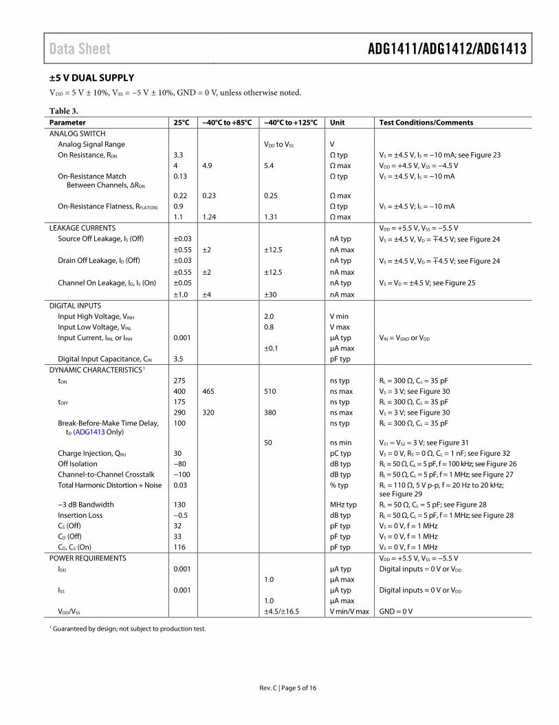
±5 V DUAL SUPPLY VDD = 5 V ± 10%, VSS = −5 V ± 10%, GND = 0 V, unless otherwise noted.
Table 3. Parameter 25°C −40°C to +85°C −40°C to +125°C Unit Test Conditions/Comments ANALOG SWITCH
Analog Signal Range VDD to VSS V On Resistance, RON 3.3 Ω typ VS = ±4.5 V, IS = −10 mA; see Figure 23 4 4.9 5.4 Ω max VDD = +4.5 V, VSS = −4.5 V On-Resistance Match
Between Channels, ∆RON 0.13 Ω typ VS = ±4.5 V, IS = −10 mA
0.22 0.23 0.25 Ω max On-Resistance Flatness, RFLAT(ON) 0.9 Ω typ VS = ±4.5 V; IS = −10 mA 1.1 1.24 1.31 Ω max
LEAKAGE CURRENTS VDD = +5.5 V, VSS = −5.5 V Source Off Leakage, IS (Off) ±0.03 nA typ VS = ±4.5 V, VD = ∓4.5 V; see Figure 24 ±0.55 ±2 ±12.5 nA max Drain Off Leakage, ID (Off) ±0.03 nA typ VS = ±4.5 V, VD = ∓4.5 V; see Figure 24
±0.55 ±2 ±12.5 nA max Channel On Leakage, ID, IS (On) ±0.05 nA typ VS = VD = ±4.5 V; see Figure 25
±1.0 ±4 ±30 nA max
DIGITAL INPUTS Input High Voltage, VINH 2.0 V min Input Low Voltage, VINL 0.8 V max Input Current, IINL or IINH 0.001 µA typ VIN = VGND or VDD ±0.1 µA max Digital Input Capacitance, CIN 3.5 pF typ
DYNAMIC CHARACTERISTICS1 tON 275 ns typ RL = 300 Ω, CL = 35 pF 400 465 510 ns max VS = 3 V; see Figure 30 tOFF 175 ns typ RL = 300 Ω, CL = 35 pF 290 320 380 ns max VS = 3 V; see Figure 30 Break-Before-Make Time Delay,
tD (ADG1413 Only) 100 ns typ RL = 300 Ω, CL = 35 pF
50 ns min VS1 = VS2 = 3 V; see Figure 31 Charge Injection, QINJ 30 pC typ VS = 0 V, RS = 0 Ω, CL = 1 nF; see Figure 32 Off Isolation −80 dB typ RL = 50 Ω, CL = 5 pF, f = 100 kHz; see Figure 26 Channel-to-Channel Crosstalk −100 dB typ RL = 50 Ω, CL = 5 pF, f = 1 MHz; see Figure 27 Total Harmonic Distortion + Noise 0.03 % typ RL = 110 Ω, 5 V p-p, f = 20 Hz to 20 kHz;
see Figure 29 −3 dB Bandwidth 130 MHz typ RL = 50 Ω, CL = 5 pF; see Figure 28 Insertion Loss −0.5 dB typ RL = 50 Ω, CL = 5 pF, f = 1 MHz; see Figure 28 CS (Off) 32 pF typ VS = 0 V, f = 1 MHz CD (Off) 33 pF typ VS = 0 V, f = 1 MHz CD, CS (On) 116 pF typ VS = 0 V, f = 1 MHz
POWER REQUIREMENTS VDD = +5.5 V, VSS = −5.5 V IDD 0.001 µA typ Digital inputs = 0 V or VDD
1.0 µA max ISS 0.001 µA typ Digital inputs = 0 V or VDD
1.0 µA max VDD/VSS ±4.5/±16.5 V min/V max GND = 0 V
1 Guaranteed by design; not subject to production test.
ADG1411/ADG1412/ADG1413 Data Sheet
Rev. C | Page 6 of 16
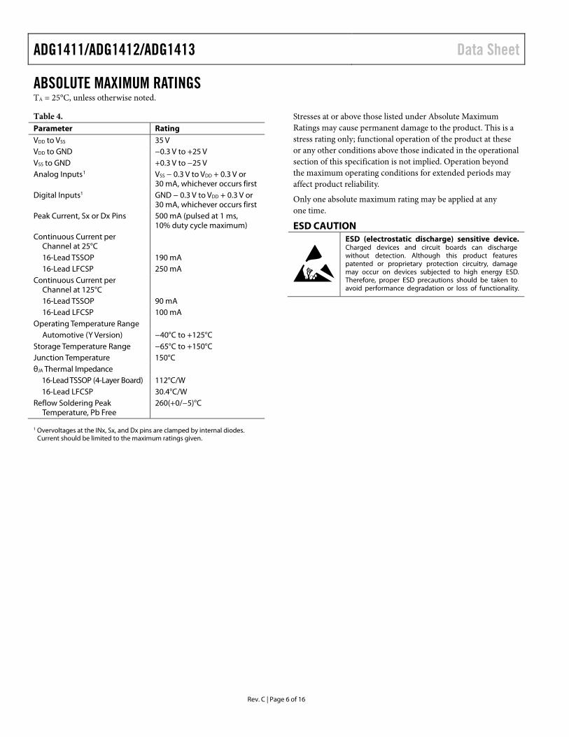
ABSOLUTE MAXIMUM RATINGS TA = 25°C, unless otherwise noted.
Table 4. Parameter Rating VDD to VSS 35 V VDD to GND −0.3 V to +25 V VSS to GND +0.3 V to −25 V Analog Inputs1 VSS − 0.3 V to VDD + 0.3 V or
30 mA, whichever occurs first Digital Inputs1 GND − 0.3 V to VDD + 0.3 V or
30 mA, whichever occurs first Peak Current, Sx or Dx Pins 500 mA (pulsed at 1 ms,
10% duty cycle maximum) Continuous Current per
Channel at 25°C
16-Lead TSSOP 190 mA 16-Lead LFCSP 250 mA
Continuous Current per Channel at 125°C
16-Lead TSSOP 90 mA 16-Lead LFCSP 100 mA
Operating Temperature Range Automotive (Y Version) −40°C to +125°C
Storage Temperature Range −65°C to +150°C Junction Temperature 150°C θJA Thermal Impedance
16-Lead TSSOP (4-Layer Board) 112°C/W 16-Lead LFCSP 30.4°C/W
Reflow Soldering Peak Temperature, Pb Free
260(+0/−5)°C
1 Overvoltages at the INx, Sx, and Dx pins are clamped by internal diodes.
Current should be limited to the maximum ratings given.
Stresses at or above those listed under Absolute Maximum Ratings may cause permanent damage to the product. This is a stress rating only; functional operation of the product at these or any other conditions above those indicated in the operational section of this specification is not implied. Operation beyond the maximum operating conditions for extended periods may affect product reliability.
Only one absolute maximum rating may be applied at any one time.
ESD CAUTION

Data Sheet ADG1411/ADG1412/ADG1413
Rev. C | Page 7 of 16
PIN CONFIGURATIONS AND FUNCTION DESCRIPTIONS
IN1 1
D1 2
S1 3
VSS 4
IN216
D215
S214
VDD13
GND 5 NIC12
S4 6 S311
D4 7 D310
IN4 8 IN39
NOTES1. NIC = NO INTERNAL CONNECTION.
ADG1411/ADG1412/ADG1413
TOP VIEW(Not to Scale)
0681
5-00
2
Figure 2. TSSOP Pin Configuration
0681
5-00
3
NOTES1. NIC = NO INTERNAL CONNECTION.2. TIE THE EXPOSED PAD TO THE SUBSTRATE, VSS.
12
11
10
1
3
4 9
2
65 7 8
16 15 14 13
S1
VSS
GND
S4
S2
D2
IN2
IN1
D1
VDD
NIC
S3
D4
IN4
IN3
D3
TOP VIEW(Not to Scale)
ADG1411/ADG1412/ADG1413
Figure 3. LFCSP Pin Configuration
Table 5. Pin Function Descriptions Pin No.
TSSOP LFCSP Mnemonic Description 1 15 IN1 Logic Control Input. 2 16 D1 Drain Terminal. This pin can be an input or output. 3 1 S1 Source Terminal. This pin can be an input or output. 4 2 VSS Most Negative Power Supply Potential. 5 3 GND Ground (0 V) Reference. 6 4 S4 Source Terminal. This pin can be an input or output. 7 5 D4 Drain Terminal. This pin can be an input or output. 8 6 IN4 Logic Control Input. 9 7 IN3 Logic Control Input. 10 8 D3 Drain Terminal. This pin can be an input or output. 11 9 S3 Source Terminal. This pin can be an input or output. 12 10 NIC No Internal Connection. 13 11 VDD Most Positive Power Supply Potential. 14 12 S2 Source Terminal. This pin can be an input or output. 15 13 D2 Drain Terminal. This pin can be an input or output. 16 14 IN2 Logic Control Input. N/A1 0 EPAD Exposed Pad. Tie the exposed pad to the substrate, VSS.
1 N/A means not applicable.
Table 6. ADG1411/ADG1412 Truth Table ADG1411 INx ADG1412 INx Switch Condition 0 1 On 1 0 Off
Table 7. ADG1413 Truth Table ADG1413 INx S1, S4 S2, S3 0 Off On 1 On Off
ADG1411/ADG1412/ADG1413 Data Sheet
Rev. C | Page 8 of 16
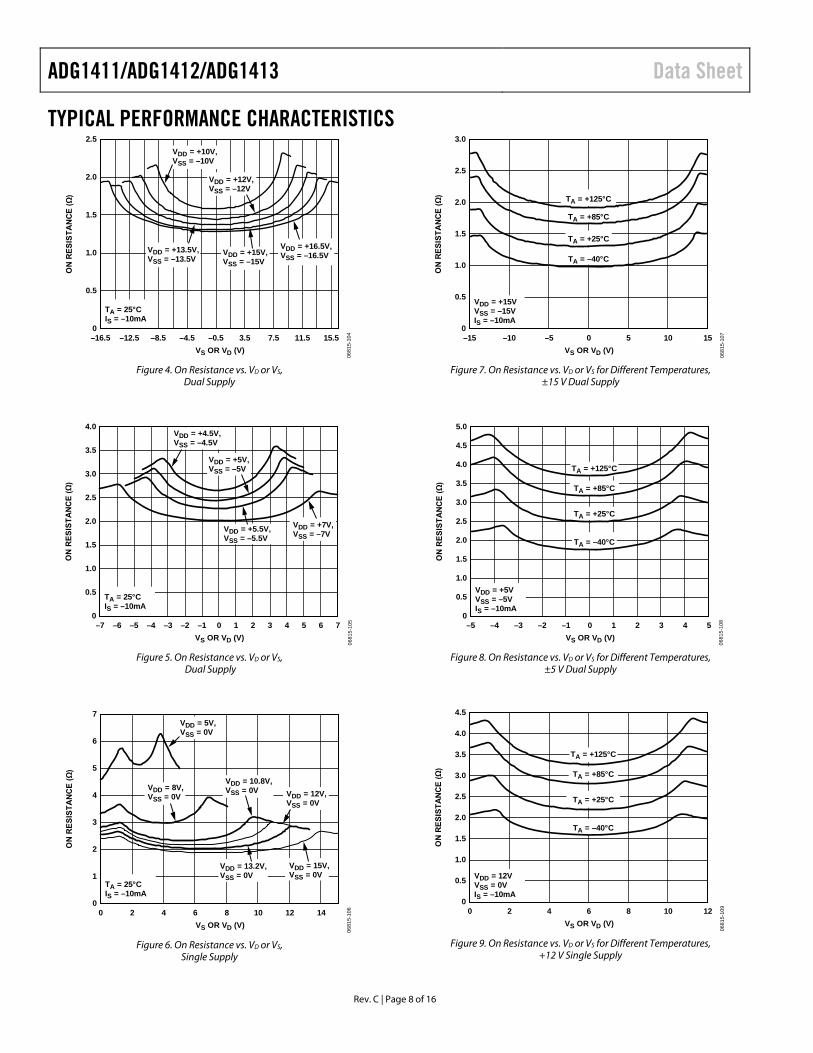
TYPICAL PERFORMANCE CHARACTERISTICS 2.5
2.0
1.5
1.0
0.5
0–16.5 –12.5 –8.5 –4.5 –0.5 3.5 7.5 15.5
ON
RES
ISTA
NC
E (Ω
)
VS OR VD (V)11.5
VDD = +16.5V,VSS = –16.5V
TA = 25°CIS = –10mA
VDD = +15V,VSS = –15V
VDD = +13.5V,VSS = –13.5V
VDD = +12V,VSS = –12V
VDD = +10V,VSS = –10V
0681
5-10
4
Figure 4. On Resistance vs. VD or VS,
Dual Supply
4.0
3.5
3.0
2.5
2.0
1.5
1.0
0.5
0–7 –6 –5 –3 –1–4 –2 0 1 6
ON
RES
ISTA
NC
E (Ω
)
VS OR VD (V)3 4 752
TA = 25°CIS = –10mA
VDD = +7V,VSS = –7VVDD = +5.5V,
VSS = –5.5V
VDD = +5V,VSS = –5V
VDD = +4.5V,VSS = –4.5V
0681
5-10
5
Figure 5. On Resistance vs. VD or VS,
Dual Supply
7
6
5
4
3
2
1
00 1412108642
ON
RES
ISTA
NC
E (Ω
)
VS OR VD (V)
TA = 25°CIS = –10mA
VDD = 15V,VSS = 0V
VDD = 13.2V,VSS = 0V
VDD = 12V,VSS = 0V
VDD = 10.8V,VSS = 0VVDD = 8V,
VSS = 0V
VDD = 5V,VSS = 0V
0681
5-10
6
Figure 6. On Resistance vs. VD or VS,
Single Supply
3.0
2.5
2.0
1.5
1.0
0.5
0–15 151050–5–10
ON
RES
ISTA
NC
E (Ω
)
VS OR VD (V)
VDD = +15VVSS = –15VIS = –10mA
TA = +25°C
TA = +85°C
TA = +125°C
TA = –40°C
0681
5-10
7
Figure 7. On Resistance vs. VD or VS for Different Temperatures,
±15 V Dual Supply
5.0
4.5
4.0
3.5
3.0
2.5
2.0
1.5
1.0
0.5
0–5 –4 –3 –2 –1 0 1 2 3 4 5
ON
RES
ISTA
NC
E (Ω
)
VS OR VD (V)
VDD = +5VVSS = –5VIS = –10mA
TA = +25°C
TA = +85°C
TA = +125°C
TA = –40°C
0681
5-10
8
Figure 8. On Resistance vs. VD or VS for Different Temperatures,
±5 V Dual Supply
4.5
4.0
3.5
3.0
2.5
2.0
1.5
1.0
0.5
00 12108642
ON
RES
ISTA
NC
E (Ω
)
VS OR VD (V)
VDD = 12VVSS = 0VIS = –10mA
TA = +25°C
TA = +85°C
TA = +125°C
TA = –40°C
0681
5-10
9
Figure 9. On Resistance vs. VD or VS for Different Temperatures,
+12 V Single Supply
Data Sheet ADG1411/ADG1412/ADG1413
Rev. C | Page 9 of 16
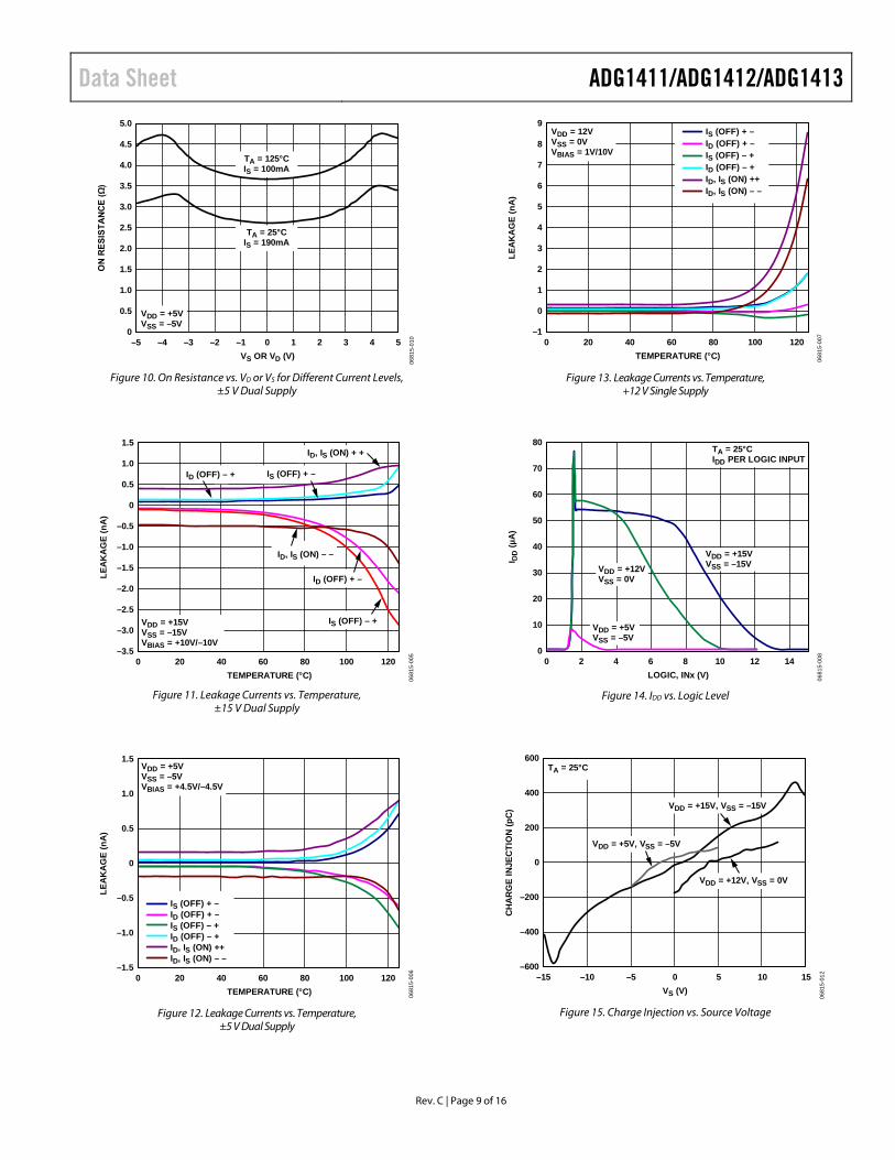
5.0
4.5
4.0
3.5
3.0
2.5
2.0
1.5
1.0
0.5
0–5 –4 –3 –2 –1 0 1 2 3 4 5
ON
RES
ISTA
NC
E (Ω
)
VS OR VD (V)
VDD = +5VVSS = –5V
TA = 125°CIS = 100mA
TA = 25°CIS = 190mA
0681
5-01
0
Figure 10. On Resistance vs. VD or VS for Different Current Levels,
±5 V Dual Supply
1.5
–3.5
–3.0
–2.5
–2.0
–1.5
–1.0
–0.5
0
0.5
1.0
0 12010080604020
LEA
KA
GE
(nA
)
TEMPERATURE (°C)
VDD = +15VVSS = –15VVBIAS = +10V/–10V
0681
5-00
5
IS (OFF) + –
ID (OFF) + –
IS (OFF) – +
ID (OFF) – +
ID, IS (ON) + +
ID, IS (ON) – –
Figure 11. Leakage Currents vs. Temperature,
±15 V Dual Supply
1.5
–1.5
–1.0
–0.5
0
0.5
1.0
0 12080 100604020
LEA
KA
GE
(nA
)
TEMPERATURE (°C)
VDD = +5VVSS = –5VVBIAS = +4.5V/–4.5V
0681
5-00
6
ID (OFF) – +
IS (OFF) + –
ID, IS (ON) ++ID, IS (ON) – –
ID (OFF) + –IS (OFF) – +
Figure 12. Leakage Currents vs. Temperature,
±5 V Dual Supply
9
8
7
6
5
4
3
2
1
0
–10 12080 100604020
LEA
KA
GE
(nA
)
TEMPERATURE (°C) 0681
5-00
7
IS (OFF) + –ID (OFF) + –IS (OFF) – +ID (OFF) – +ID, IS (ON) ++ID, IS (ON) – –
VDD = 12VVSS = 0VVBIAS = 1V/10V
Figure 13. Leakage Currents vs. Temperature, +12 V Single Supply
80
70
60
50
40
30
20
10
00 1412108642
I DD
(µA
)
LOGIC, INx (V)
TA = 25°CIDD PER LOGIC INPUT
VDD = +15VVSS = –15VVDD = +12V
VSS = 0V
VDD = +5VVSS = –5V
0681
5-00
8
Figure 14. IDD vs. Logic Level
600
400
200
0
–200
–400
–600–15 –10 –5 0 5 10 15
CH
AR
GE
INJE
CTI
ON
(pC
)
VS (V)
VDD = +15V, VSS = –15V
VDD = +12V, VSS = 0V
VDD = +5V, VSS = –5V
TA = 25°C
0681
5-01
2
Figure 15. Charge Injection vs. Source Voltage
ADG1411/ADG1412/ADG1413 Data Sheet
Rev. C | Page 10 of 16
300
0
50
100
150
200
250
–40 –20 0 20 40 60 80 120
TIM
E (n
s)
TEMPERATURE (°C)100
0681
5-01
3
15V DS tON
15V DS tOFF
12V SS tON
12V SS tOFF
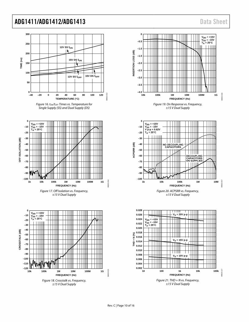
Figure 16. tON/tOFF Times vs. Temperature for
Single Supply (SS) and Dual Supply (DS)
0
–100
–90
–80
–70
–60
–50
–40
–30
–20
–10
1k 10k 100k 1M 10M 1G100M
OFF
ISO
LATI
ON
(dB
)
FREQUENCY (Hz)
VDD = +15VVSS = –15VTA = 25°C
0681
5-01
4
Figure 17. Off Isolation vs. Frequency,
±15 V Dual Supply
0
–120
–110
–100
–90
–80
–70
–60
–50
–40
–30
–20
–10
10k 100k 1M 10M 100M 1G
CR
OSS
TALK
(dB
)
FREQUENCY (Hz)
VDD = +15VVSS = –15VTA = 25°C
0681
5-01
5
Figure 18. Crosstalk vs. Frequency,
±15 V Dual Supply
0
–4.0
–3.5
–3.0
–2.5
–2.0
–1.5
–1.0
–0.5
10k 100k 1M 10M 1G100M
INSE
RTI
ON
LO
SS (d
B)
FREQUENCY (Hz)
VDD = +15VVSS = –15VTA = 25°C
0681
5-01
6
Figure 19. On Response vs. Frequency,
±15 V Dual Supply
0
–100
–90
–80
–70
–60
–50
–40
–30
–20
–10
1k 10k 100k 1M 10M
AC
PSR
R (d
B)
FREQUENCY (Hz)
VDD = +15VVSS = –15VV p-p = 0.62VTA = 25°C
NO DECOUPLINGCAPACITORS
DECOUPLINGCAPACITORSON SUPPLIES
0681
5-01
7
Figure 20. ACPSRR vs. Frequency,
±15 V Dual Supply
0.028
0.024
0.026
0.022
0.020
0.018
0.016
0.014
0.012
0.010
0.008
0.006
0.004
0.00210 100 1k 10k 100k
THD
+ N
(%)
FREQUENCY (Hz)
VDD = +15VVSS = –15VTA = 25°C
VS = 20V p-p
VS = 15V p-p
0681
5-11
7
VS = 10V p-p
Figure 21. THD + N vs. Frequency,
±15 V Dual Supply
Data Sheet ADG1411/ADG1412/ADG1413
Rev. C | Page 11 of 16
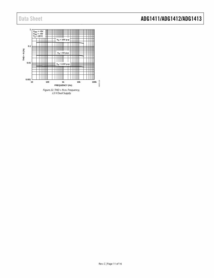
1
0.1
0.01
0.00110 100 1k 10k 100k
THD
+ N
(%)
FREQUENCY (Hz)
VDD = +5VVSS = –5VTA = 25°C
VS = 10V p-p
VS = 5V p-p
VS = 2.5V p-p
0681
5-11
8
Figure 22. THD + N vs. Frequency,
±5 V Dual Supply
ADG1411/ADG1412/ADG1413 Data Sheet
Rev. C | Page 12 of 16
TERMINOLOGY IDD The positive supply current.
ISS The negative supply current.
VD, VS The analog voltage on Terminal D and Terminal S.
RON The ohmic resistance between Terminal D and Terminal S.
RFLAT(ON) Flatness is defined as the difference between the maximum and minimum value of on resistance measured over the specified analog signal range.
IS (Off) The source leakage current with the switch off.
ID (Off) The drain leakage current with the switch off.
ID, IS (On) The channel leakage current with the switch on.
VINL The maximum input voltage for Logic 0.
VINH The minimum input voltage for Logic 1.
IINL, IINH The input current of the digital input when high or when low.
CS (Off) The off switch source capacitance, which is measured with reference to ground.
CD (Off) The off switch drain capacitance, which is measured with reference to ground.
CD, CS (On) The on switch capacitance, which is measured with reference to ground.
CIN The digital input capacitance.
tON The delay between applying the digital control input and the output switching on. See Figure 30.
tOFF The delay between applying the digital control input and the output switching off.
Charge Injection A measure of the glitch impulse transferred from the digital input to the analog output during switching.
Off Isolation A measure of unwanted signal coupling through an off switch.
Crosstalk A measure of unwanted signal that is coupled through from one channel to another as a result of parasitic capacitance.
Bandwidth The frequency at which the output is attenuated by 3 dB.
On Response The frequency response of the on switch.
Insertion Loss The loss due to the on resistance of the switch.
Total Harmonic Distortion + Noise (THD + N) The ratio of the harmonic amplitude plus noise of the signal to the fundamental.
AC Power Supply Rejection Ratio (ACPSRR) A measure of the ability of the device to avoid coupling noise and spurious signals that appear on the supply voltage pin to the output of the switch. The dc voltage on the device is modulated by a sine wave of 0.62 V p-p. The ratio of the amplitude of the signal on the output to the amplitude of the modulation is the ACPSRR.
Data Sheet ADG1411/ADG1412/ADG1413
Rev. C | Page 13 of 16
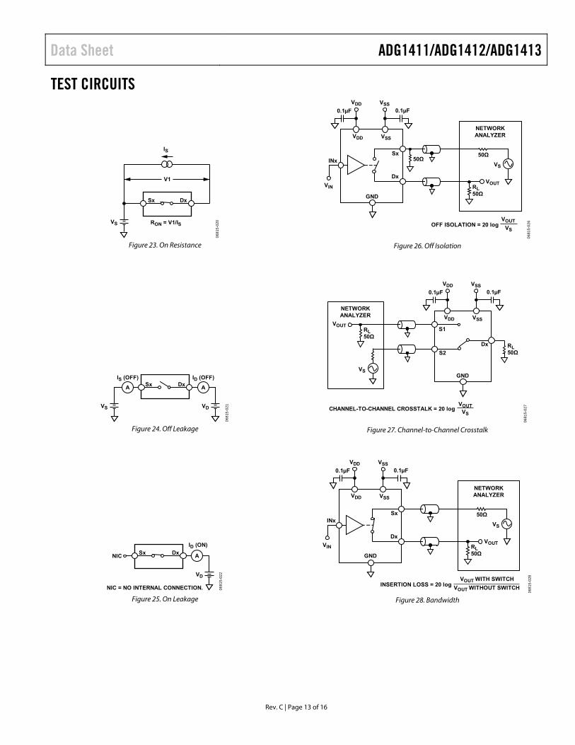
TEST CIRCUITS
Sx Dx
VS
IS
V1
RON = V1/IS06
815-
020
Figure 23. On Resistance
Sx Dx
VS
A A
VD
IS (OFF) ID (OFF)
0681
5-02
1
Figure 24. Off Leakage
Sx DxA
VD
ID (ON)
NIC
NIC = NO INTERNAL CONNECTION. 0681
5-02
2
Figure 25. On Leakage
VOUT
50Ω
NETWORKANALYZER
RL50Ω
INx
VIN
Sx
Dx
50Ω
OFF ISOLATION = 20 logVOUT
VS
VS
VDD VSS
0.1µF
VDD
0.1µF
VSS
GND
0681
5-02
6
Figure 26. Off Isolation
CHANNEL-TO-CHANNEL CROSSTALK = 20 logVOUT
GND
S1
Dx
S2
VOUT
NETWORKANALYZER
RL50Ω
RL50Ω
VS
VS
VDD VSS
0.1µF
VDD
0.1µF
VSS
0681
5-02
7
Figure 27. Channel-to-Channel Crosstalk
VOUT
50Ω
NETWORKANALYZER
RL50Ω
INx
VIN
Sx
Dx
INSERTION LOSS = 20 logVOUT WITH SWITCH
VOUT WITHOUT SWITCH
VS
VDD VSS
0.1µF
VDD
0.1µF
VSS
GND
0681
5-02
8
Figure 28. Bandwidth
ADG1411/ADG1412/ADG1413 Data Sheet
Rev. C | Page 14 of 16
VOUT
RS
AUDIO PRECISION
RL110Ω
INx
VIN
Sx
Dx
VSV p-p
VDD VSS
0.1µFVDD
0.1µFVSS
GND
0681
5-02
9
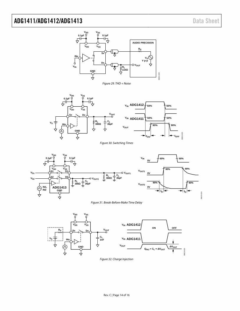
Figure 29. THD + Noise
VS INx
Sx Dx
GND
RL300Ω
CL35pF
VOUT
VDD VSS
0.1µFVDD
0.1µFVSS
ADG1412
ADG1411
VIN
VIN
VOUT
tON tOFF
50% 50%
90% 90%
50% 50%
0681
5-02
3
Figure 30. Switching Times
VS2
IN1,IN2
S2 D2
VS1S1 D1
GND
RL300Ω
CL35pF
VOUT2
VOUT1
VDD VSS
0.1µFVDD
0.1µFVSS
VIN
VOUT1
VOUT2ADG1413
tD tD
50% 50%
90%90%
90%90%
0V
0V
0V
RL300Ω
CL35pF
0681
5-02
4
Figure 31. Break-Before-Make Time Delay
INx
VOUT
ADG1412
ADG1411
VIN
VIN
VOUT
OFF
ΔVOUT
ON
QINJ = CL × ΔVOUT
Sx Dx
VDD VSS
VDD VSS
VS
RS
GND
CL1nF
0681
5-02
5
Figure 32. Charge Injection
Data Sheet ADG1411/ADG1412/ADG1413
Rev. C | Page 15 of 16
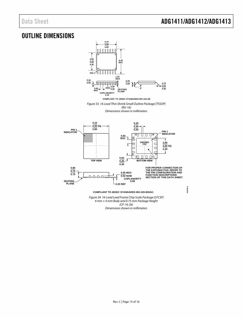
OUTLINE DIMENSIONS
16 9
81
PIN 1
SEATINGPLANE
8°0°
4.504.404.30
6.40BSC
5.105.004.90
0.65BSC
0.150.05
1.20MAX
0.200.09 0.75
0.600.45
0.300.19
COPLANARITY0.10
COMPLIANT TO JEDEC STANDARDS MO-153-AB Figure 33. 16-Lead Thin Shrink Small Outline Package [TSSOP]
(RU-16) Dimensions shown in millimeters
COMPLIANT TO JEDEC STANDARDS MO-220-WGGC. 0427
09-A
10.65BSC
BOTTOM VIEWTOP VIEW
16
589
1213
4
EXPOSEDPAD
PIN 1INDICATOR
4.104.00 SQ3.90
0.500.400.30
SEATINGPLANE
0.800.750.70 0.05 MAX
0.02 NOM
0.20 REF
COPLANARITY0.08
PIN 1INDICATOR
0.350.300.25
2.602.50 SQ2.40
FOR PROPER CONNECTION OFTHE EXPOSED PAD, REFER TOTHE PIN CONFIGURATION ANDFUNCTION DESCRIPTIONSSECTION OF THIS DATA SHEET.
Figure 34. 16-Lead Lead Frame Chip Scale Package [LFCSP]
4 mm × 4 mm Body and 0.75 mm Package Height (CP-16-26)
Dimensions shown in millimeters
ADG1411/ADG1412/ADG1413 Data Sheet
Rev. C | Page 16 of 16
ORDERING GUIDE Model1, 2 Temperature Range Package Description Package Option ADG1411YRUZ −40°C to +125°C 16-Lead Thin Shrink Small Outline Package [TSSOP] RU-16 ADG1411YRUZ-REEL7 −40°C to +125°C 16-Lead Thin Shrink Small Outline Package [TSSOP] RU-16 ADG1411YCPZ-REEL −40°C to +125°C 16-Lead Lead Frame Chip Scale Package [LFCSP] CP-16-26 ADG1411YCPZ-REEL7 −40°C to +125°C 16-Lead Lead Frame Chip Scale Package [LFCSP] CP-16-26 ADG1411WBCPZ-REEL −40°C to +125°C 16-Lead Lead Frame Chip Scale Package [LFCSP] CP-16-26 ADG1412YRUZ −40°C to +125°C 16-Lead Thin Shrink Small Outline Package [TSSOP] RU-16 ADG1412YRUZ-REEL7 −40°C to +125°C 16-Lead Thin Shrink Small Outline Package [TSSOP] RU-16 ADG1412YCPZ-REEL −40°C to +125°C 16-Lead Lead Frame Chip Scale Package [LFCSP] CP-16-26 ADG1412YCPZ-REEL7 −40°C to +125°C 16-Lead Lead Frame Chip Scale Package [LFCSP] CP-16-26 ADG1413YRUZ −40°C to +125°C 16-Lead Thin Shrink Small Outline Package [TSSOP] RU-16 ADG1413YRUZ-REEL7 −40°C to +125°C 16-Lead Thin Shrink Small Outline Package [TSSOP] RU-16 ADG1413YCPZ-REEL −40°C to +125°C 16-Lead Lead Frame Chip Scale Package [LFCSP] CP-16-26 ADG1413YCPZ-REEL7 −40°C to +125°C 16-Lead Lead Frame Chip Scale Package [LFCSP] CP-16-26 1 Z = RoHS Compliant Part. 2 W = qualified for automotive applications.
AUTOMOTIVE PRODUCTS The ADG1411W model is available with controlled manufacturing to support the quality and reliability requirements of automotive applications. Note that this automotive model may have specifications that differ from the commercial models; therefore, designers should review the Specifications section of this data sheet carefully. Only the automotive grade product shown is available for use in automotive applications. Contact your local Analog Devices account representative for specific product ordering information and to obtain the specific Automotive Reliability reports for this model.
©2008–2016 Analog Devices, Inc. All rights reserved. Trademarks and registered trademarks are the property of their respective owners. D06815-0-3/16(C)