8-bit microcontrollers - fujitsu … · 8-bit microcontrollers cmos f2mc-8fx mb95260h/270h/280h...
TRANSCRIPT

FUJITSU MICROELECTRONICSDATA SHEET DS07–12627–1E
8-bit MicrocontrollersCMOS
F2MC-8FX MB95260H/270H/280H SeriesMB95F262H/F262K/F263H/F263K/F264H/F264KMB95F272H/F272K/F273H/F273K/F274H/F274KMB95F282H/F282K/F283H/F283K/F284H/F284K DESCRIPTION
MB95260H/270H/280H are series of general-purpose, single-chip microcontrollers. In addition to a compactinstruction set, the microcontrollers of these series contain a variety of peripheral resources.
Note: F2MC is the abbreviation of FUJITSU Flexible Microcontroller.
FEATURES• F2MC-8FX CPU core
Instruction set optimized for controllers• Multiplication and division instructions• 16-bit arithmetic operations• Bit test branch instructions• Bit manipulation instructions, etc.
• Clock (main OSC clock and sub-OSC clock are only available in MB95F262H/F262K/F263H/F263K/F264H/F264K/F282H/F282K/F283H/F283K/F284H/F284K)
• Selectable main clock sourceMain OSC clock (up to 16.25 MHz, maximum machine clock frequency: 8.125 MHz)External clock (up to 32.5 MHz, maximum machine clock frequency: 16.25 MHz)Main internal CR clock (1/8/10 MHz ±3%, maximum machine clock frequency: 10 MHz)
• Selectable subclock sourceSub-OSC clock (32.768 kHz)External clock (32.768 kHz)Sub-internal CR clock (Typ: 100 kHz, Min: 50 kHz, Max: 200 kHz)
• Timer• 8/16-bit composite timer• Timebase timer• Watch prescaler
• LIN-UART (MB95F262H/F262K/F263H/F263K/F264H/F264K/F282H/F282K/F283H/F283K/F284H/F284K)• Full duplex double buffer• Capable of clock-synchronized serial data transfer and clock-asynchronized serial data transfer
(Continued)
Copyright©2008 FUJITSU MICROELECTRONICS LIMITED All rights reserved2008.12
MB95260H/270H/280H Series
(Continued)• External interrupt
• Interrupt by edge detection (rising edge, falling edge, and both edges can be selected)• Can be used to wake up the device from different low power consumption (standby) modes
• 8/10-bit A/D converter• 8-bit or 10-bit resolution can be selected.
• Low power consumption (standby) modes• Stop mode• Sleep mode• Watch mode• Timebase timer mode
• I/O port (Max: 17) (MB95F262K/F263K/F264K)• General-purpose I/O ports (Max):
CMOS I/O: 15, N-ch open drain: 2• I/O port (Max: 16) (MB95F262H/F263H/F264H)
• General-purpose I/O ports (Max):CMOS I/O: 15, N-ch open drain: 1
• I/O port (Max: 5) (MB95F272K/F273K/F274K)• General-purpose I/O ports (Max):
CMOS I/O: 3, N-ch open drain: 2• I/O port (Max: 4) (MB95F272H/F273H/F274H)
• General-purpose I/O ports (Max):CMOS I/O: 3, N-ch open drain: 1
• I/O port (Max: 13) (MB95F282K/F283K/F284K)• General-purpose I/O ports (Max):
CMOS I/O: 11, N-ch open drain: 2• I/O port (Max: 12) (MB95F282H/F283H/F284H)
• General-purpose I/O ports (Max):CMOS I/O: 11, N-ch open drain: 1
• On-chip debug• 1-wire serial control• Serial writing supported (asynchronous mode)
• Hardware/software watchdog timer• Built-in hardware watchdog timer
• Low-voltage detection reset circuit• Built-in low-voltage detector
• Clock supervisor counter• Built-in clock supervisor counter function
• Programmable port input voltage level• CMOS input level / hysteresis input level
• Dual operation Flash memory• The erase/write operation and the read operation can be executed in different banks (upper bank/lower
bank) simultaneously.• Flash memory security function
• Protects the content of the Flash memory
2 DS07–12627–1E
MB95260H/270H/280H Series
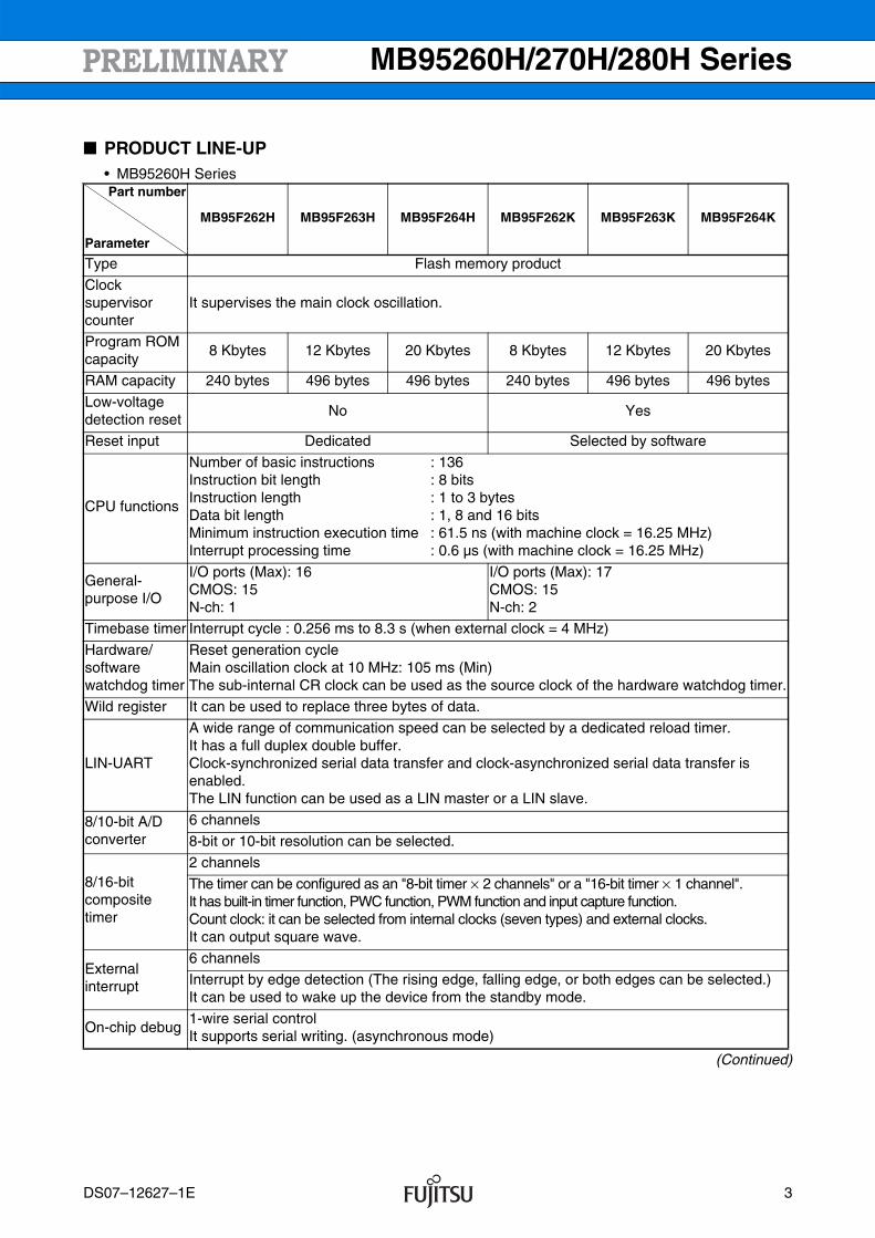
PRODUCT LINE-UP• MB95260H Series
(Continued)
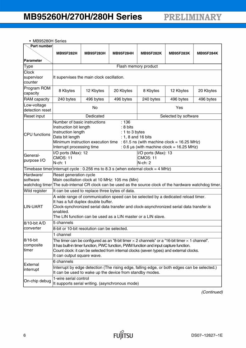
Part number
Parameter
MB95F262H MB95F263H MB95F264H MB95F262K MB95F263K MB95F264K
Type Flash memory product
Clock supervisor counter
It supervises the main clock oscillation.
Program ROM capacity
8 Kbytes 12 Kbytes 20 Kbytes 8 Kbytes 12 Kbytes 20 Kbytes
RAM capacity 240 bytes 496 bytes 496 bytes 240 bytes 496 bytes 496 bytes
Low-voltagedetection reset
No Yes
Reset input Dedicated Selected by software
CPU functions
Number of basic instructions : 136Instruction bit length : 8 bitsInstruction length : 1 to 3 bytesData bit length : 1, 8 and 16 bitsMinimum instruction execution time : 61.5 ns (with machine clock = 16.25 MHz) Interrupt processing time : 0.6 µs (with machine clock = 16.25 MHz)
General-purpose I/O
I/O ports (Max): 16CMOS: 15N-ch: 1
I/O ports (Max): 17CMOS: 15N-ch: 2
Timebase timer Interrupt cycle : 0.256 ms to 8.3 s (when external clock = 4 MHz)
Hardware/software watchdog timer
Reset generation cycleMain oscillation clock at 10 MHz: 105 ms (Min)The sub-internal CR clock can be used as the source clock of the hardware watchdog timer.
Wild register It can be used to replace three bytes of data.
LIN-UART
A wide range of communication speed can be selected by a dedicated reload timer.It has a full duplex double buffer. Clock-synchronized serial data transfer and clock-asynchronized serial data transfer is enabled.The LIN function can be used as a LIN master or a LIN slave.
8/10-bit A/D converter
6 channels
8-bit or 10-bit resolution can be selected.
8/16-bitcomposite timer
2 channels
The timer can be configured as an "8-bit timer × 2 channels" or a "16-bit timer × 1 channel".It has built-in timer function, PWC function, PWM function and input capture function.Count clock: it can be selected from internal clocks (seven types) and external clocks.It can output square wave.
External interrupt
6 channels
Interrupt by edge detection (The rising edge, falling edge, or both edges can be selected.)It can be used to wake up the device from the standby mode.
On-chip debug1-wire serial controlIt supports serial writing. (asynchronous mode)
DS07–12627–1E 3
MB95260H/270H/280H Series
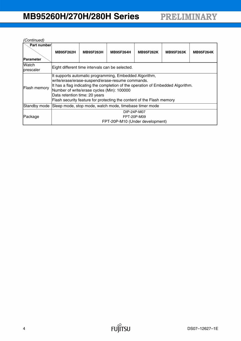
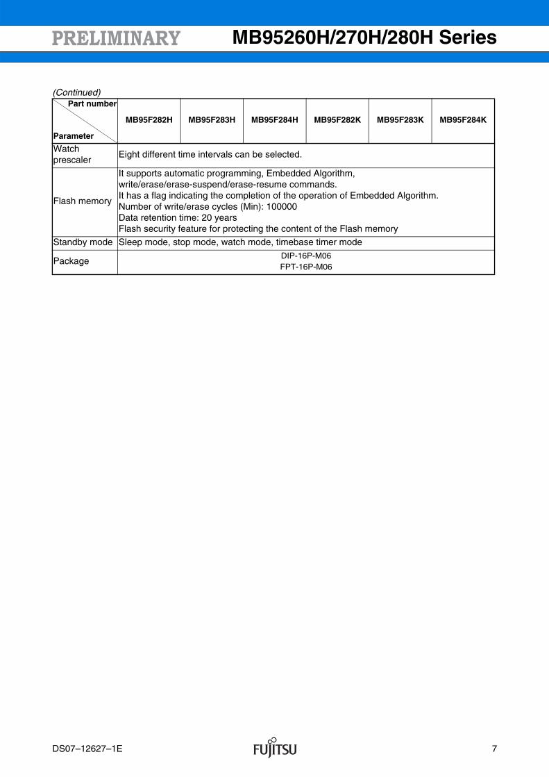
(Continued)Part number
Parameter
MB95F262H MB95F263H MB95F264H MB95F262K MB95F263K MB95F264K
Watch prescaler
Eight different time intervals can be selected.
Flash memory
It supports automatic programming, Embedded Algorithm,write/erase/erase-suspend/erase-resume commands.It has a flag indicating the completion of the operation of Embedded Algorithm.Number of write/erase cycles (Min): 100000Data retention time: 20 yearsFlash security feature for protecting the content of the Flash memory
Standby mode Sleep mode, stop mode, watch mode, timebase timer mode
PackageDIP-24P-M07FPT-20P-M09
FPT-20P-M10 (Under development)
4 DS07–12627–1E
MB95260H/270H/280H Series
• MB95270H SeriesPart number
Parameter
MB95F272H MB95F273H MB95F274H MB95F272K MB95F273K MB95F274K
Type Flash memory product
Clock supervisor counter
It supervises the main clock oscillation.
Program ROM capacity
8 Kbytes 12 Kbytes 20 Kbytes 8 Kbytes 12 Kbytes 20 Kbytes
RAM capacity 240 bytes 496 bytes 496 bytes 240 bytes 496 bytes 496 bytes
Low-voltagedetection reset
No Yes
Reset input Dedicated Selected by software
CPU functions
Number of basic instructions : 136Instruction bit length : 8 bitsInstruction length : 1 to 3 bytesData bit length : 1, 8 and 16 bitsMinimum instruction execution time : 61.5 ns (with machine clock = 16.25 MHz)Interrupt processing time : 0.6 µs (with machine clock = 16.25 MHz)
General-purpose I/O
I/O ports (Max): 4CMOS: 3N-ch: 1
I/O ports (Max): 5CMOS: 3N-ch: 2
Timebase timer Interrupt cycle : 0.256 ms to 8.3 s (when external clock = 4 MHz)
Hardware/software watchdog timer
Reset generation cycleMain oscillation clock at 10 MHz: 105 ms (Min)The sub-internal CR clock can be used as the source clock of the hardware watchdog timer.
Wild register It can be used to replace three bytes of data.
LIN-UART No LIN-UART
8/10-bit A/D converter
2 channels
8-bit or 10-bit resolution can be selected.
8/16-bitcomposite timer
1 channel
The timer can be configured as an "8-bit timer × 2 channels" or a "16-bit timer × 1 channel".It has built-in timer function, PWC function, PWM function and input capture function.Count clock: it can be selected from internal clocks (seven types) and external clocks.It can output square wave.
External interrupt
2 channels
Interrupt by edge detection (The rising edge, falling edge, or both edges can be selected.)It can be used to wake up the device from standby modes.
On-chip debug1-wire serial controlIt supports serial writing. (asynchronous mode)
Watch prescaler
Eight different time intervals can be selected.
Flash memory
It supports automatic programming, Embedded Algorithm,write/erase/erase-suspend/erase-resume commands.It has a flag indicating the completion of the operation of Embedded Algorithm.Number of write/erase cycles (Min): 100000Data retention time: 20 yearsFlash security feature for protecting the content of the Flash memory
Standby mode Sleep mode, stop mode, watch mode, timebase timer mode
PackageDIP-8P-M03FPT-8P-M08
DS07–12627–1E 5
MB95260H/270H/280H Series
• MB95280H Series
(Continued)
Part number
Parameter
MB95F282H MB95F283H MB95F284H MB95F282K MB95F283K MB95F284K
Type Flash memory product
Clock supervisor counter
It supervises the main clock oscillation.
Program ROM capacity
8 Kbytes 12 Kbytes 20 Kbytes 8 Kbytes 12 Kbytes 20 Kbytes
RAM capacity 240 bytes 496 bytes 496 bytes 240 bytes 496 bytes 496 bytes
Low-voltagedetection reset
No Yes
Reset input Dedicated Selected by software
CPU functions
Number of basic instructions : 136Instruction bit length : 8 bitsInstruction length : 1 to 3 bytesData bit length : 1, 8 and 16 bitsMinimum instruction execution time : 61.5 ns (with machine clock = 16.25 MHz) Interrupt processing time : 0.6 µs (with machine clock = 16.25 MHz)
General-purpose I/O
I/O ports (Max): 12CMOS: 11N-ch: 1
I/O ports (Max): 13CMOS: 11N-ch: 2
Timebase timer Interrupt cycle : 0.256 ms to 8.3 s (when external clock = 4 MHz)
Hardware/software watchdog timer
Reset generation cycleMain oscillation clock at 10 MHz: 105 ms (Min)The sub-internal CR clock can be used as the source clock of the hardware watchdog timer.
Wild register It can be used to replace three bytes of data.
LIN-UART
A wide range of communication speed can be selected by a dedicated reload timer.It has a full duplex double buffer.Clock-synchronized serial data transfer and clock-asynchronized serial data transfer is enabled.The LIN function can be used as a LIN master or a LIN slave.
8/10-bit A/D converter
5 channels
8-bit or 10-bit resolution can be selected.
8/16-bitcomposite timer
1 channel
The timer can be configured as an "8-bit timer × 2 channels" or a "16-bit timer × 1 channel".It has built-in timer function, PWC function, PWM function and input capture function.Count clock: it can be selected from internal clocks (seven types) and external clocks.It can output square wave.
External interrupt
6 channels
Interrupt by edge detection (The rising edge, falling edge, or both edges can be selected.)It can be used to wake up the device from standby modes.
On-chip debug1-wire serial controlIt supports serial writing. (asynchronous mode)
6 DS07–12627–1E
MB95260H/270H/280H Series
(Continued)Part number
Parameter
MB95F282H MB95F283H MB95F284H MB95F282K MB95F283K MB95F284K
Watch prescaler
Eight different time intervals can be selected.
Flash memory
It supports automatic programming, Embedded Algorithm,write/erase/erase-suspend/erase-resume commands.It has a flag indicating the completion of the operation of Embedded Algorithm.Number of write/erase cycles (Min): 100000Data retention time: 20 yearsFlash security feature for protecting the content of the Flash memory
Standby mode Sleep mode, stop mode, watch mode, timebase timer mode
PackageDIP-16P-M06FPT-16P-M06
DS07–12627–1E 7
MB95260H/270H/280H Series
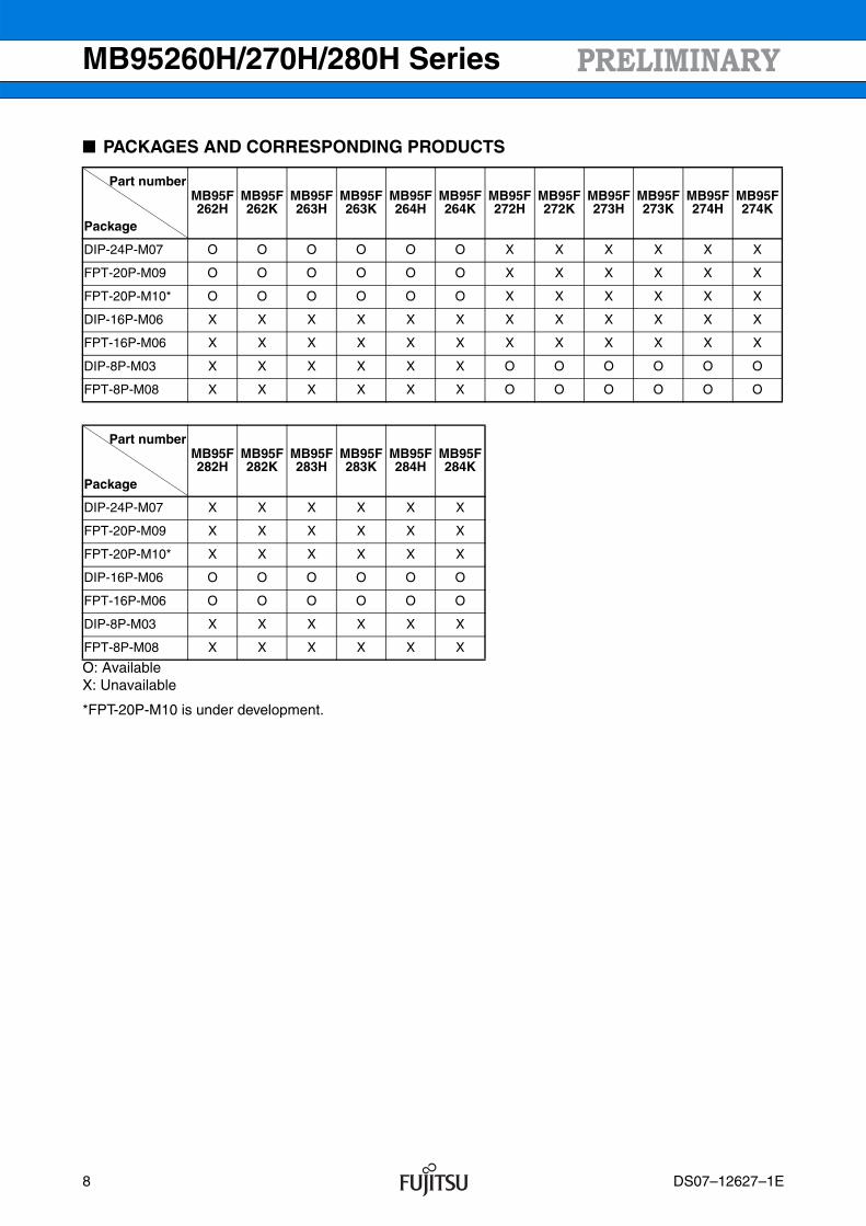
PACKAGES AND CORRESPONDING PRODUCTS
O: AvailableX: Unavailable
*FPT-20P-M10 is under development.
Part number
Package
MB95F262H
MB95F262K
MB95F263H
MB95F263K
MB95F264H
MB95F264K
MB95F272H
MB95F272K
MB95F273H
MB95F273K
MB95F274H
MB95F274K
DIP-24P-M07 O O O O O O X X X X X X
FPT-20P-M09 O O O O O O X X X X X X
FPT-20P-M10* O O O O O O X X X X X X
DIP-16P-M06 X X X X X X X X X X X X
FPT-16P-M06 X X X X X X X X X X X X
DIP-8P-M03 X X X X X X O O O O O O
FPT-8P-M08 X X X X X X O O O O O O
Part number
Package
MB95F282H
MB95F282K
MB95F283H
MB95F283K
MB95F284H
MB95F284K
DIP-24P-M07 X X X X X X
FPT-20P-M09 X X X X X X
FPT-20P-M10* X X X X X X
DIP-16P-M06 O O O O O O
FPT-16P-M06 O O O O O O
DIP-8P-M03 X X X X X X
FPT-8P-M08 X X X X X X
8 DS07–12627–1E
MB95260H/270H/280H Series
DIFFERENCES AMONG PRODUCTS AND NOTES ON PRODUCT SELECTION• Current consumption
When using the on-chip debug function, take account of the current consumption of flash erase/write.
For details of current consumption, see “ ELECTRICAL CHARACTERISTICS”.
• Package
For details of information on each package, see “ PACKAGES AND CORRESPONDING PRODUCTS” and“ PACKAGE DIMENSIONS”.
• Operating voltage
The operating voltage varies, depending on whether the on-chip debug function is used or not.
For details of the operating voltage, see “ ELECTRICAL CHARACTERISTICS”.
• On-chip debug function
The on-chip debug function requires that VCC, VSS and 1 serial-wire be connected to an evaluation tool. Inaddition, if the Flash memory data has to be updated, the RST/PF2 pin must also be connected to the sameevaluation tool.
DS07–12627–1E 9
MB95260H/270H/280H Series
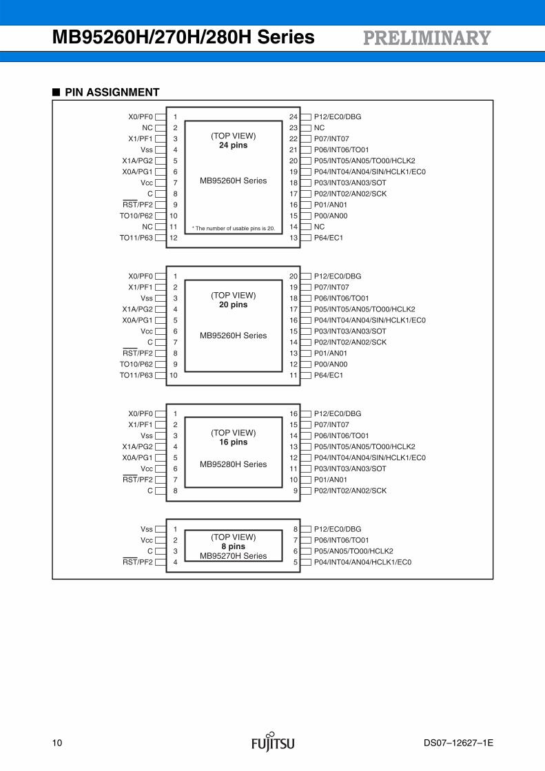
PIN ASSIGNMENT
P12/EC0/DBG
NC
P07/INT07
P06/INT06/TO01
P05/INT05/AN05/TO00/HCLK2
P04/INT04/AN04/SIN/HCLK1/EC0
P03/INT03/AN03/SOT
P02/INT02/AN02/SCK
P01/AN01
P00/AN00
NC
P64/EC1
X0/PF0
NC
X1/PF1
Vss
X1A/PG2
X0A/PG1
Vcc MB95260H Series
MB95260H Series
MB95280H Series
MB95270H Series
C
RST/PF2
TO10/P62
NC
TO11/P63
(TOP VIEW)24 pins
24
23
22
21
20
19
18
17
16
15
14
13
1
2
3
4
5
6
7
8
9
10
11
12
P12/EC0/DBG
P06/INT06/TO01
P05/AN05/TO00/HCLK2
P04/INT04/AN04/HCLK1/EC0
Vss
Vcc
C
RST/PF2
(TOP VIEW)8 pins
8
7
6
5
1
2
3
4
* The number of usable pins is 20.
P12/EC0/DBG
P07/INT07
P06/INT06/TO01
P05/INT05/AN05/TO00/HCLK2
P04/INT04/AN04/SIN/HCLK1/EC0
P03/INT03/AN03/SOT
P02/INT02/AN02/SCK
P01/AN01
P00/AN00
P64/EC1
X0/PF0
X1/PF1
Vss
X1A/PG2
X0A/PG1
Vcc
C
RST/PF2
TO10/P62
TO11/P63
(TOP VIEW)20 pins
20
19
18
17
16
15
14
13
12
11
1
2
3
4
5
6
7
8
9
10
P12/EC0/DBG
P07/INT07
P06/INT06/TO01
P05/INT05/AN05/TO00/HCLK2
P04/INT04/AN04/SIN/HCLK1/EC0
P03/INT03/AN03/SOT
P01/AN01
P02/INT02/AN02/SCK
X0/PF0
X1/PF1
Vss
X1A/PG2
X0A/PG1
Vcc
RST/PF2
C
(TOP VIEW)16 pins
16
15
14
13
12
11
10
9
1
2
3
4
5
6
7
8
10 DS07–12627–1E
MB95260H/270H/280H Series
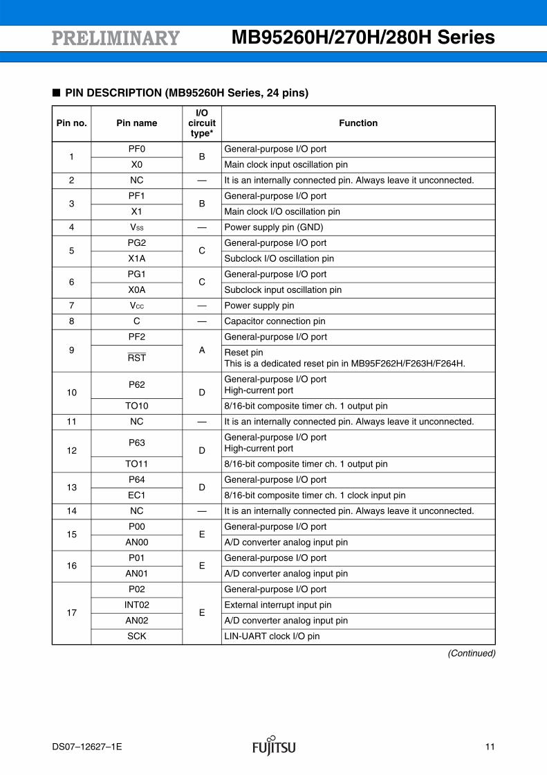
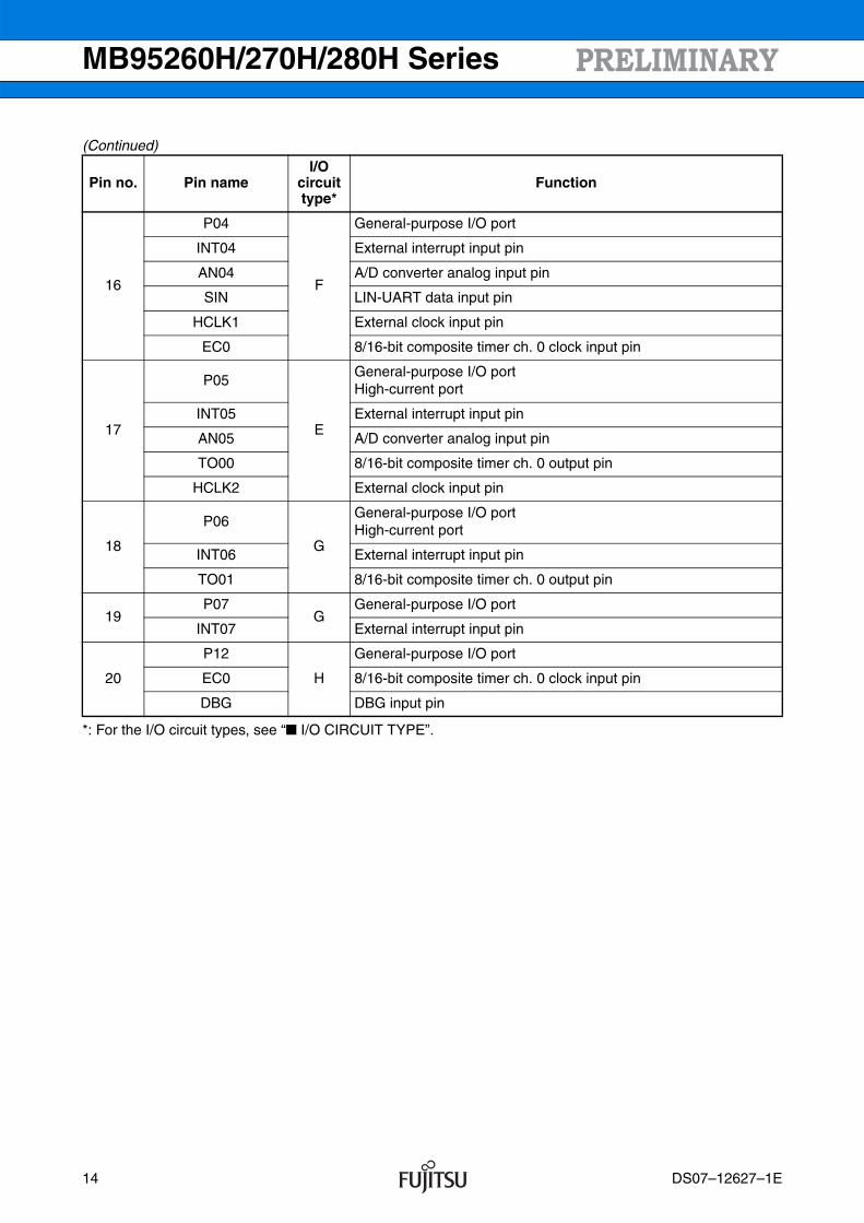
PIN DESCRIPTION (MB95260H Series, 24 pins)
(Continued)
Pin no. Pin nameI/O
circuit type*
Function
1PF0
BGeneral-purpose I/O port
X0 Main clock input oscillation pin
2 NC — It is an internally connected pin. Always leave it unconnected.
3PF1
BGeneral-purpose I/O port
X1 Main clock I/O oscillation pin
4 VSS — Power supply pin (GND)
5PG2
CGeneral-purpose I/O port
X1A Subclock I/O oscillation pin
6PG1
CGeneral-purpose I/O port
X0A Subclock input oscillation pin
7 VCC — Power supply pin
8 C — Capacitor connection pin
9
PF2
A
General-purpose I/O port
RSTReset pinThis is a dedicated reset pin in MB95F262H/F263H/F264H.
10P62
D
General-purpose I/O portHigh-current port
TO10 8/16-bit composite timer ch. 1 output pin
11 NC — It is an internally connected pin. Always leave it unconnected.
12P63
D
General-purpose I/O portHigh-current port
TO11 8/16-bit composite timer ch. 1 output pin
13P64
DGeneral-purpose I/O port
EC1 8/16-bit composite timer ch. 1 clock input pin
14 NC — It is an internally connected pin. Always leave it unconnected.
15P00
EGeneral-purpose I/O port
AN00 A/D converter analog input pin
16P01
EGeneral-purpose I/O port
AN01 A/D converter analog input pin
17
P02
E
General-purpose I/O port
INT02 External interrupt input pin
AN02 A/D converter analog input pin
SCK LIN-UART clock I/O pin
DS07–12627–1E 11
MB95260H/270H/280H Series
(Continued)
*: For the I/O circuit types, see “ I/O CIRCUIT TYPE”.
Pin no. Pin nameI/O
circuit type*
Function
18
P03
E
General-purpose I/O port
INT03 External interrupt input pin
AN03 A/D converter analog input pin
SOT LIN-UART data output pin
19
P04
F
General-purpose I/O port
INT04 External interrupt input pin
AN04 A/D converter analog input pin
SIN LIN-UART data input pin
HCLK1 External clock input pin
EC0 8/16-bit composite timer ch. 0 clock input pin
20
P05
E
General-purpose I/O portHigh-current port
INT05 External interrupt input pin
AN05 A/D converter analog input pin
TO00 8/16-bit composite timer ch. 0 output pin
HCLK2 External clock input pin
21
P06
G
General-purpose I/O portHigh-current port
INT06 External interrupt input pin
TO01 8/16-bit composite timer ch. 0 output pin
22P07
GGeneral-purpose I/O port
INT07 External interrupt input pin
23 NC — It is an internally connected pin. Always leave it unconnected.
24
P12
H
General-purpose I/O port
EC0 8/16-bit composite timer ch. 0 clock input pin
DBG DBG input pin
12 DS07–12627–1E
MB95260H/270H/280H Series
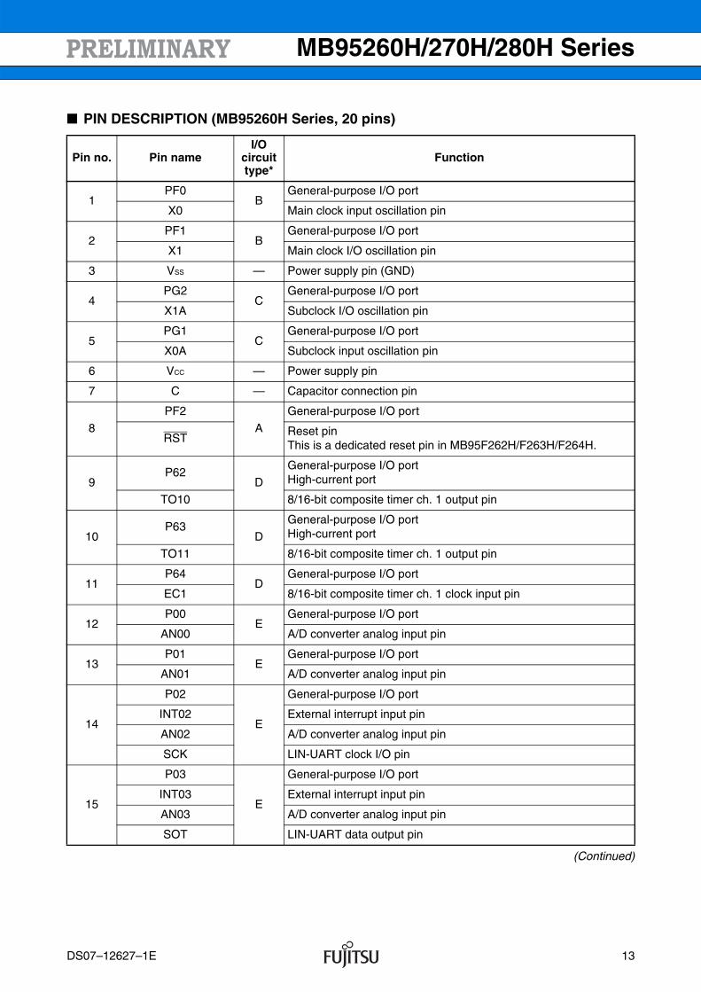
PIN DESCRIPTION (MB95260H Series, 20 pins)
(Continued)
Pin no. Pin nameI/O
circuit type*
Function
1PF0
BGeneral-purpose I/O port
X0 Main clock input oscillation pin
2PF1
BGeneral-purpose I/O port
X1 Main clock I/O oscillation pin
3 VSS — Power supply pin (GND)
4PG2
CGeneral-purpose I/O port
X1A Subclock I/O oscillation pin
5PG1
CGeneral-purpose I/O port
X0A Subclock input oscillation pin
6 VCC — Power supply pin
7 C — Capacitor connection pin
8
PF2
A
General-purpose I/O port
RSTReset pinThis is a dedicated reset pin in MB95F262H/F263H/F264H.
9P62
D
General-purpose I/O portHigh-current port
TO10 8/16-bit composite timer ch. 1 output pin
10P63
D
General-purpose I/O portHigh-current port
TO11 8/16-bit composite timer ch. 1 output pin
11P64
DGeneral-purpose I/O port
EC1 8/16-bit composite timer ch. 1 clock input pin
12P00
EGeneral-purpose I/O port
AN00 A/D converter analog input pin
13P01
EGeneral-purpose I/O port
AN01 A/D converter analog input pin
14
P02
E
General-purpose I/O port
INT02 External interrupt input pin
AN02 A/D converter analog input pin
SCK LIN-UART clock I/O pin
15
P03
E
General-purpose I/O port
INT03 External interrupt input pin
AN03 A/D converter analog input pin
SOT LIN-UART data output pin
DS07–12627–1E 13
MB95260H/270H/280H Series
(Continued)
*: For the I/O circuit types, see “ I/O CIRCUIT TYPE”.
Pin no. Pin nameI/O
circuit type*
Function
16
P04
F
General-purpose I/O port
INT04 External interrupt input pin
AN04 A/D converter analog input pin
SIN LIN-UART data input pin
HCLK1 External clock input pin
EC0 8/16-bit composite timer ch. 0 clock input pin
17
P05
E
General-purpose I/O portHigh-current port
INT05 External interrupt input pin
AN05 A/D converter analog input pin
TO00 8/16-bit composite timer ch. 0 output pin
HCLK2 External clock input pin
18
P06
G
General-purpose I/O portHigh-current port
INT06 External interrupt input pin
TO01 8/16-bit composite timer ch. 0 output pin
19P07
GGeneral-purpose I/O port
INT07 External interrupt input pin
20
P12
H
General-purpose I/O port
EC0 8/16-bit composite timer ch. 0 clock input pin
DBG DBG input pin
14 DS07–12627–1E
MB95260H/270H/280H Series
s
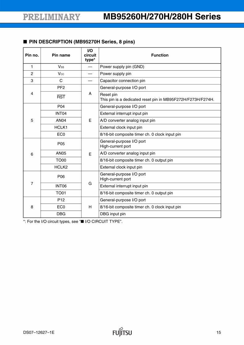
PIN DESCRIPTION (MB95270H Series, 8 pins)
*: For the I/O circuit types, see “ I/O CIRCUIT TYPE”.
Pin no. Pin nameI/O
circuit type*
Function
1 VSS — Power supply pin (GND)
2 VCC — Power supply pin
3 C — Capacitor connection pin
4
PF2
A
General-purpose I/O port
RSTReset pinThis pin is a dedicated reset pin in MB95F272H/F273H/F274H.
5
P04
E
General-purpose I/O port
INT04 External interrupt input pin
AN04 A/D converter analog input pin
HCLK1 External clock input pin
EC0 8/16-bit composite timer ch. 0 clock input pin
6
P05
E
General-purpose I/O portHigh-current port
AN05 A/D converter analog input pin
TO00 8/16-bit composite timer ch. 0 output pin
HCLK2 External clock input pin
7
P06
G
General-purpose I/O portHigh-current port
INT06 External interrupt input pin
TO01 8/16-bit composite timer ch. 0 output pin
8
P12
H
General-purpose I/O port
EC0 8/16-bit composite timer ch. 0 clock input pin
DBG DBG input pin
DS07–12627–1E 15
MB95260H/270H/280H Series
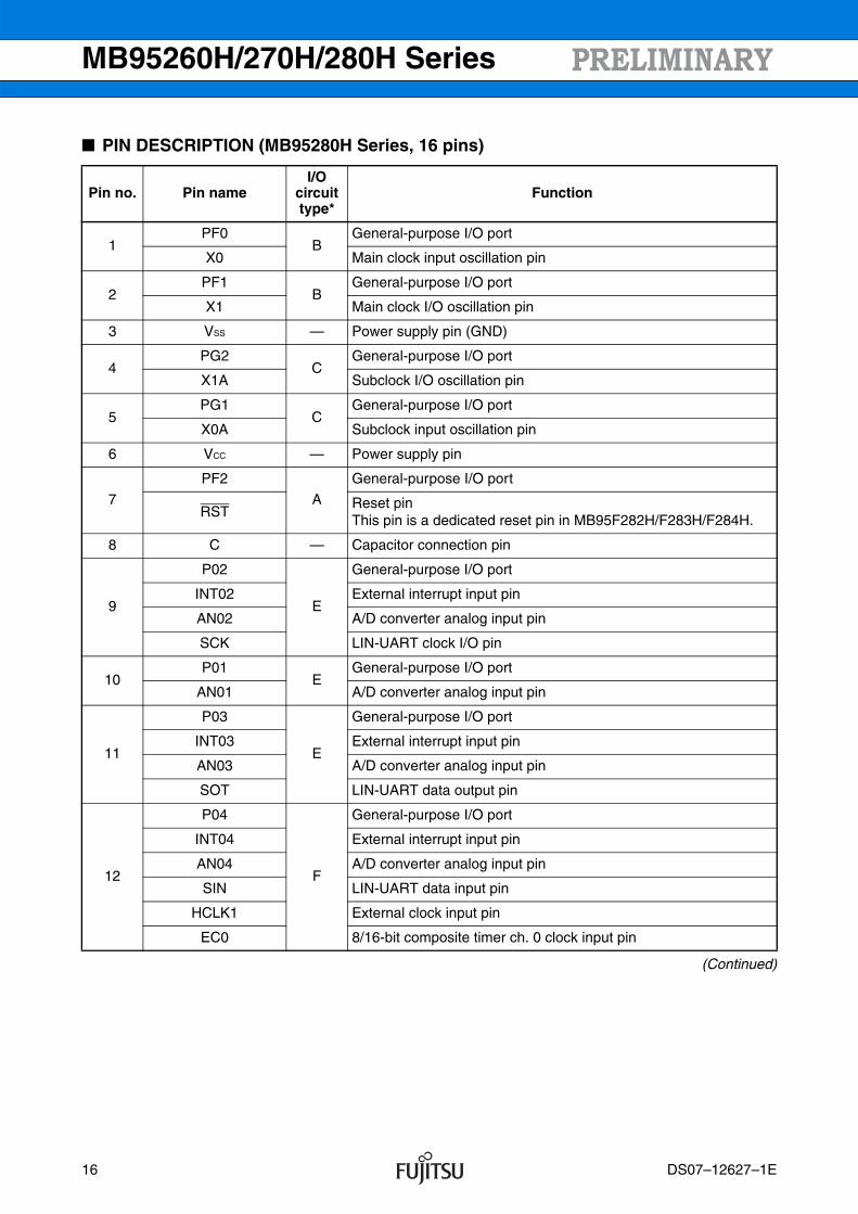
PIN DESCRIPTION (MB95280H Series, 16 pins)
(Continued)
Pin no. Pin nameI/O
circuit type*
Function
1PF0
BGeneral-purpose I/O port
X0 Main clock input oscillation pin
2PF1
BGeneral-purpose I/O port
X1 Main clock I/O oscillation pin
3 VSS — Power supply pin (GND)
4PG2
CGeneral-purpose I/O port
X1A Subclock I/O oscillation pin
5PG1
CGeneral-purpose I/O port
X0A Subclock input oscillation pin
6 VCC — Power supply pin
7
PF2
A
General-purpose I/O port
RSTReset pinThis pin is a dedicated reset pin in MB95F282H/F283H/F284H.
8 C — Capacitor connection pin
9
P02
E
General-purpose I/O port
INT02 External interrupt input pin
AN02 A/D converter analog input pin
SCK LIN-UART clock I/O pin
10P01
EGeneral-purpose I/O port
AN01 A/D converter analog input pin
11
P03
E
General-purpose I/O port
INT03 External interrupt input pin
AN03 A/D converter analog input pin
SOT LIN-UART data output pin
12
P04
F
General-purpose I/O port
INT04 External interrupt input pin
AN04 A/D converter analog input pin
SIN LIN-UART data input pin
HCLK1 External clock input pin
EC0 8/16-bit composite timer ch. 0 clock input pin
16 DS07–12627–1E
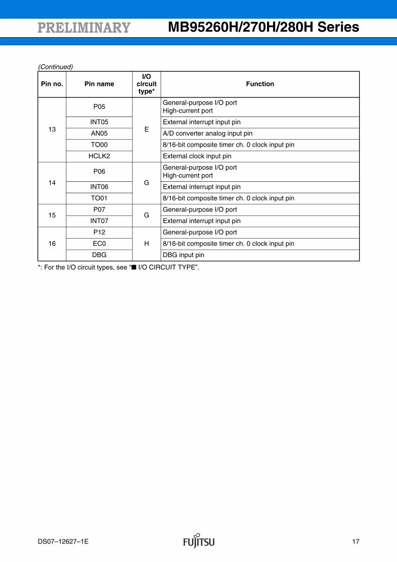
MB95260H/270H/280H Series
(Continued)
*: For the I/O circuit types, see “ I/O CIRCUIT TYPE”.
Pin no. Pin nameI/O
circuit type*
Function
13
P05
E
General-purpose I/O portHigh-current port
INT05 External interrupt input pin
AN05 A/D converter analog input pin
TO00 8/16-bit composite timer ch. 0 clock input pin
HCLK2 External clock input pin
14
P06
G
General-purpose I/O portHigh-current port
INT06 External interrupt input pin
TO01 8/16-bit composite timer ch. 0 clock input pin
15P07
GGeneral-purpose I/O port
INT07 External interrupt input pin
16
P12
H
General-purpose I/O port
EC0 8/16-bit composite timer ch. 0 clock input pin
DBG DBG input pin
DS07–12627–1E 17
MB95260H/270H/280H Series
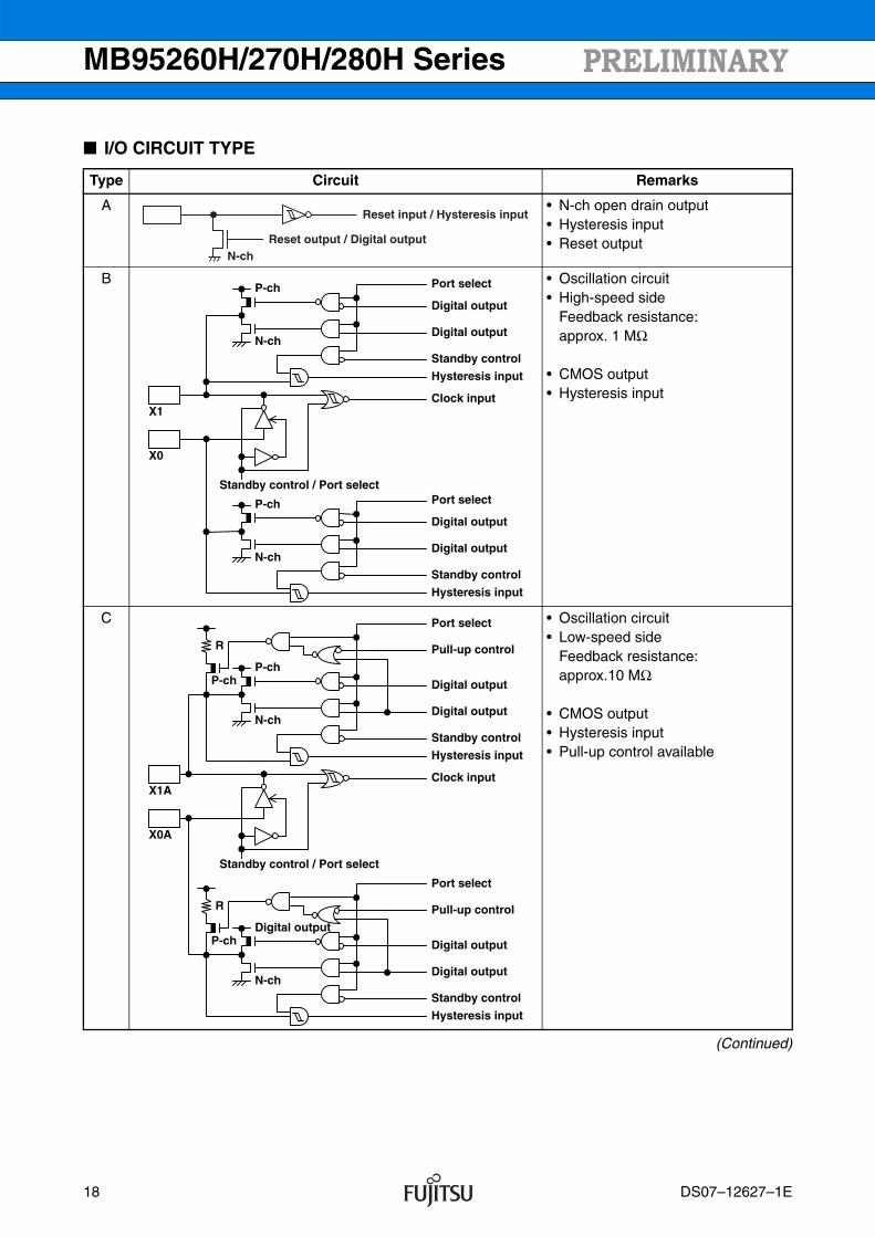
I/O CIRCUIT TYPE
(Continued)
Type Circuit Remarks
A • N-ch open drain output• Hysteresis input• Reset output
B • Oscillation circuit• High-speed side
Feedback resistance:approx. 1 MΩ
• CMOS output• Hysteresis input
C • Oscillation circuit• Low-speed side
Feedback resistance: approx.10 MΩ
• CMOS output• Hysteresis input• Pull-up control available
N-chReset output / Digital output
Reset input / Hysteresis input
Standby control / Port select
Clock input
Port select
Digital output
Digital output
Standby control
Hysteresis input
Digital output
Digital output
Standby control
Hysteresis input
Port select
X1
X0
N-ch
P-ch
N-ch
P-ch
Clock inputX1A
X0A
Standby control / Port select
N-ch
P-ch
Port select
Digital output
Digital output
Standby control
Hysteresis input
N-ch
Digital output
Digital output
Digital output
Standby control
Hysteresis input
P-ch
R Pull-up control
Port select
P-ch
R Pull-up control
18 DS07–12627–1E
MB95260H/270H/280H Series
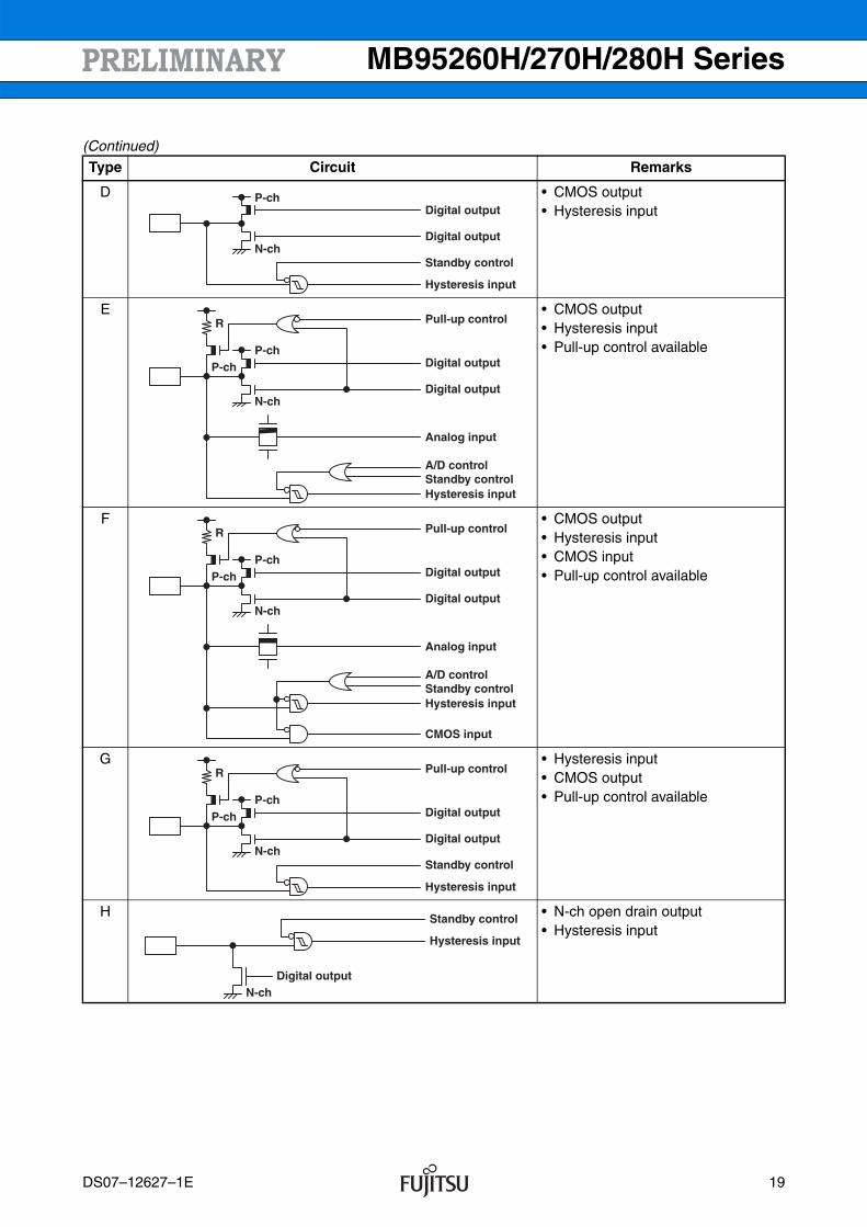
(Continued)
Type Circuit Remarks
D • CMOS output• Hysteresis input
E • CMOS output• Hysteresis input• Pull-up control available
F • CMOS output• Hysteresis input• CMOS input• Pull-up control available
G • Hysteresis input• CMOS output• Pull-up control available
H • N-ch open drain output• Hysteresis input
N-ch
P-chDigital output
Digital output
Standby control
Hysteresis input
N-ch
P-chP-ch
R Pull-up control
Digital output
Digital output
Analog input
A/D controlStandby controlHysteresis input
N-ch
P-chP-ch
R Pull-up control
Digital output
Digital output
Analog input
A/D controlStandby controlHysteresis input
CMOS input
N-ch
P-chP-ch
R Pull-up control
Digital output
Digital output
Standby control
Hysteresis input
N-ch
Standby control
Hysteresis input
Digital output
DS07–12627–1E 19
MB95260H/270H/280H Series
NOTES ON DEVICE HANDLING• Preventing latch-ups
When using the device, ensure that the voltage applied does not exceed the maximum voltage rating.In a CMOS IC, if a voltage higher than VCC or a voltage lower than VSS is applied to an input/output pin thatis neither a medium-withstand voltage pin nor a high-withstand voltage pin, or if a voltage out of the ratingrange of power supply voltage mentioned in "1. Absolute Maximum Ratings" of “ ELECTRICAL CHAR-ACTERISTICS” is applied to the VCC pin or the VSS pin, a latch-up may occur.When a latch-up occurs, power supply current increases significantly, which may cause a component to bethermally destroyed.
• Stabilizing supply voltageSupply voltage must be stabilized.A malfunction may occur when power supply voltage fluctuates rapidly even though the fluctuation is withinthe guaranteed operating range of the VCC power supply voltage.As a rule of voltage stabilization, suppress voltage fluctuation so that the fluctuation in VCC ripple (p-p value)at the commercial frequency (50 Hz/60 Hz) does not exceed 10% of the standard VCC value, and the transientfluctuation rate does not exceed 0.1 V/ms at a momentary fluctuation such as switching the power supply.
• Notes on using the external clockWhen an external clock is used, oscillation stabilization wait time is required for power-on reset, wake-upfrom subclock mode or stop mode.
PIN CONNECTION• Treatment of unused pins
If an unused input pin is left unconnected, a component may be permanently damaged due to malfunctionsor latch-ups. Always pull up or pull down an unused input pin through a resistor of at least 2 kΩ. Set anunused input/output pin to the output state and leave it unconnected, or set it to the input state and treat itthe same as an unused input pin. If there is an unused output pin, leave it unconnected.
• Power supply pinsTo reduce unnecessary electro-magnetic emission, prevent malfunctions of strobe signals due to an increasein the ground level, and conform to the total output current standard, always connect the VCC pin and the VSS
pin to the power supply and ground outside the device. In addition, connect the current supply source to theVCC pin and the VSS pin with low impedance.It is also advisable to connect a ceramic capacitor of approximately 0.1 µF as a bypass capacitor betweenthe VCC pin and the VSS pin at a location close to this device.
• DBG pinConnect the DBG pin directly to an external pull-up resistor.To prevent the device from unintentionally entering the debug mode due to noise, minimize the distancebetween the DBG pin and the VCC or VSS pin when designing the layout of the printed circuit board.The DBG pin should not stay at “L” level after power-on until the reset output is released.
• RST pinConnect the RST pin directly to an external pull-up resistor.To prevent the device from unintentionally entering the reset mode due to noise, minimize the distancebetween the RST pin and the VCC or VSS pin when designing the layout of the printed circuit board.The RST/PF2 pin functions as the reset input/output pin after power-on. In addition, the reset output of theRST/PF2 pin can be enabled by the RSTOE bit of the SYSC register, and the reset input function and thegeneral purpose I/O function can be selected by the RSTEN bit of the SYSC register.
20 DS07–12627–1E
MB95260H/270H/280H Series
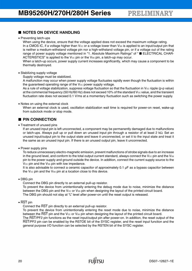
• C pinUse a ceramic capacitor or a capacitor with equivalent frequency characteristics. The bypass capacitor forthe VCC pin must have a capacitance larger than CS. For the connection to a smoothing capacitor CS, seethe diagram below. To prevent the device from unintentionally entering a mode to which the device is not setto transit due to noise, minimize the distance between the C pin and CS and the distance between CS andthe VSS pin when designing the layout of a printed circuit board.
C
Cs
DBG
RST
• DBG/RST/C pin connection diagram
DS07–12627–1E 21
MB95260H/270H/280H Series
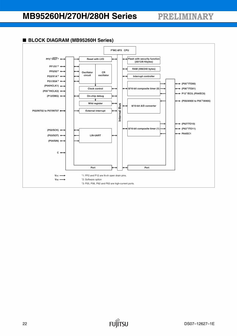
BLOCK DIAGRAM (MB95260H Series)
Flash with security function(20/12/8 Kbytes)
RAM (496/240 bytes)
Interrupt controller
8/10-bit A/D converter
8/16-bit composite timer (0)
Reset with LVD
Oscillatorcircuit
CRoscillator
Clock control
On-chip debug
Wild register
External interrupt
LIN-UART
Port Port
F2MC-8FX CPU
Inte
rnal
Bu
s
(P05*3/TO00)
(P06*3/TO01)
P12*1/EC0, (P04/EC0)
8/16-bit composite timer (1)
(P623/TO10)
(P63*3/TO11)
P64/EC1
(P00/AN00 to P05*3/AN05)
PF2*1/RST*2
PF1/X1*2
PF0/X0*2
PG2/X1A*2
PG1/X0A*2
(P04/HCLK1)
(P05*3/HCLK2)
(P12/DBG)
P02/INT02 to P07/INT07
(P02/SCK)
(P03/SOT)
(P04/SIN)
C
VCC
VSS
*1: PF2 and P12 are N-ch open drain pins.
*2: Software option
*3: P05, P06, P62 and P63 are high-current ports.
22 DS07–12627–1E
MB95260H/270H/280H Series
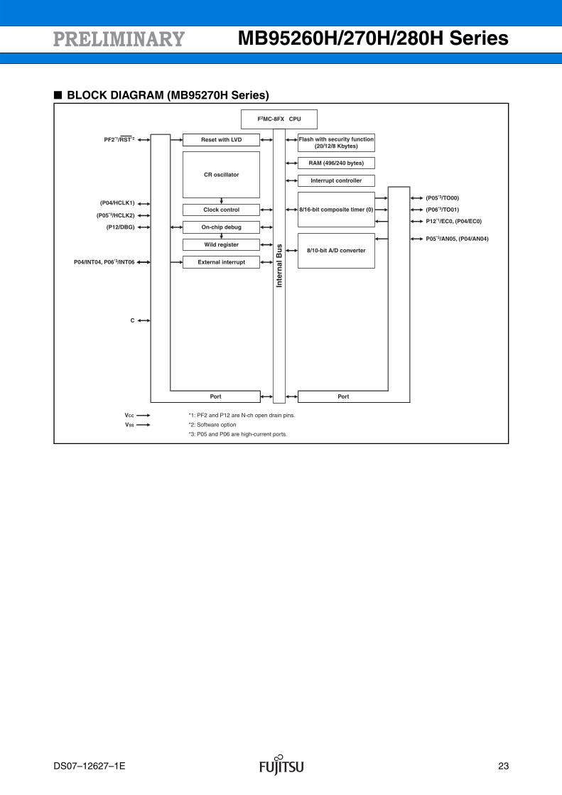
BLOCK DIAGRAM (MB95270H Series)
Flash with security function(20/12/8 Kbytes)
RAM (496/240 bytes)
Interrupt controller
8/10-bit A/D converter
8/16-bit composite timer (0)
Reset with LVD
CR oscillator
Clock control
On-chip debug
Wild register
External interrupt
Port Port
F2MC-8FX CPU
Inte
rnal
Bu
s
(P05*3/TO00)
(P06*3/TO01)
P12*1/EC0, (P04/EC0)
P05*3/AN05, (P04/AN04)
(P04/HCLK1)
(P05*3/HCLK2)
(P12/DBG)
P04/INT04, P06*3/INT06
C
VCC
VSS
*1: PF2 and P12 are N-ch open drain pins.
*2: Software option
*3: P05 and P06 are high-current ports.
PF2*1/RST*2
DS07–12627–1E 23
MB95260H/270H/280H Series
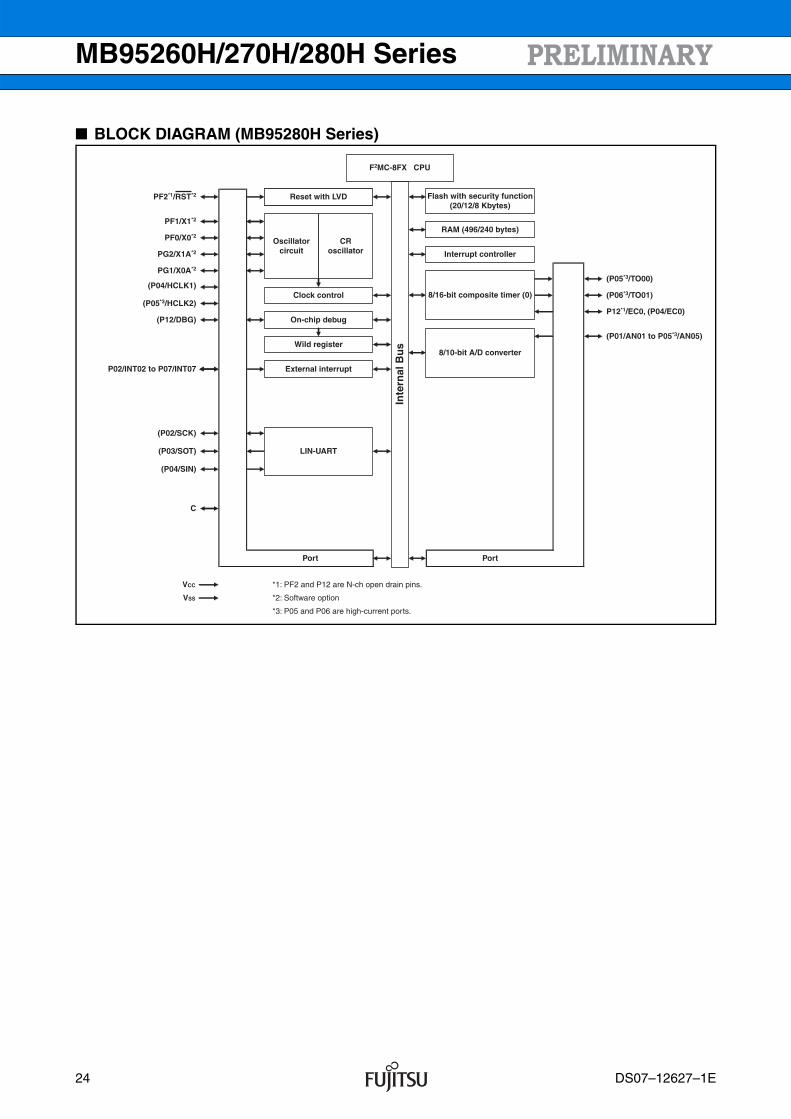
BLOCK DIAGRAM (MB95280H Series)
Flash with security function(20/12/8 Kbytes)
RAM (496/240 bytes)
Interrupt controller
8/10-bit A/D converter
8/16-bit composite timer (0)
Reset with LVD
Oscillatorcircuit
CRoscillator
Clock control
On-chip debug
Wild register
External interrupt
LIN-UART
Port Port
F2MC-8FX CPU
Inte
rnal
Bu
s
(P05*3/TO00)
(P06*3/TO01)
P12*1/EC0, (P04/EC0)
(P01/AN01 to P05*3/AN05)
PF1/X1*2
PF0/X0*2
PG2/X1A*2
PG1/X0A*2
(P04/HCLK1)
(P05*3/HCLK2)
(P12/DBG)
P02/INT02 to P07/INT07
(P02/SCK)
(P03/SOT)
(P04/SIN)
C
VCC
VSS
*1: PF2 and P12 are N-ch open drain pins.
*2: Software option
*3: P05 and P06 are high-current ports.
PF2*1/RST*2
24 DS07–12627–1E
MB95260H/270H/280H Series
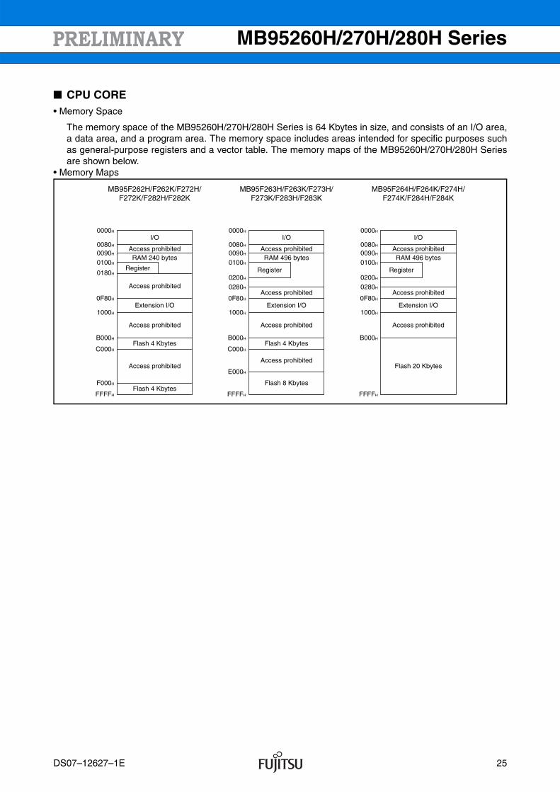
CPU CORE• Memory Space
The memory space of the MB95260H/270H/280H Series is 64 Kbytes in size, and consists of an I/O area,a data area, and a program area. The memory space includes areas intended for specific purposes suchas general-purpose registers and a vector table. The memory maps of the MB95260H/270H/280H Seriesare shown below.
• Memory Maps
I/O
Access prohibitedRAM 496 bytes
Register
Access prohibited
Extension I/O
Access prohibited
Flash 20 Kbytes
0000H
0080H
0090H
0100H
0200H
0280H
0F80H
1000H
B000H
FFFFH
MB95F264H/F264K/F274H/F274K/F284H/F284K
I/O
Access prohibitedRAM 496 bytes
Register
Access prohibited
Access prohibited
Extension I/O
Access prohibited
Flash 8 Kbytes
0000H
0080H
0090H
0100H
0280H
0200H
0F80H
1000H
B000H
C000H
E000H
FFFFH
MB95F263H/F263K/F273H/F273K/F283H/F283K
I/O
Access prohibitedRAM 240 bytes
Register
Access prohibited
Extension I/O
Access prohibited
Access prohibited
Flash 4 Kbytes
Flash 4 Kbytes Flash 4 Kbytes
0000H
0080H
0090H
0100H
0180H
0F80H
1000H
B000H
C000H
F000H
FFFFH
MB95F262H/F262K/F272H/F272K/F282H/F282K
DS07–12627–1E 25
MB95260H/270H/280H Series
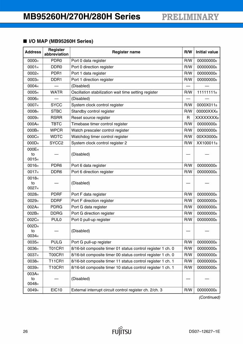
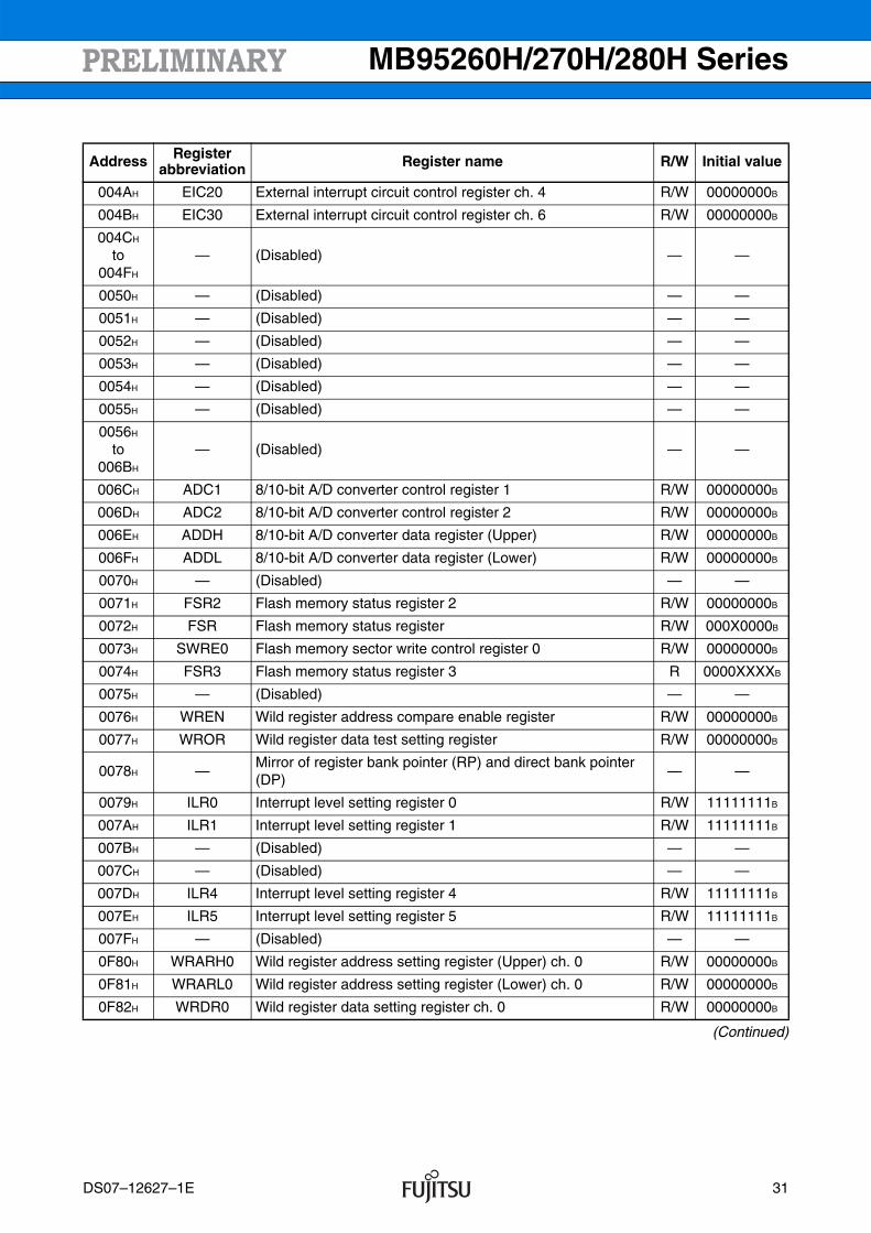
I/O MAP (MB95260H Series)
(Continued)
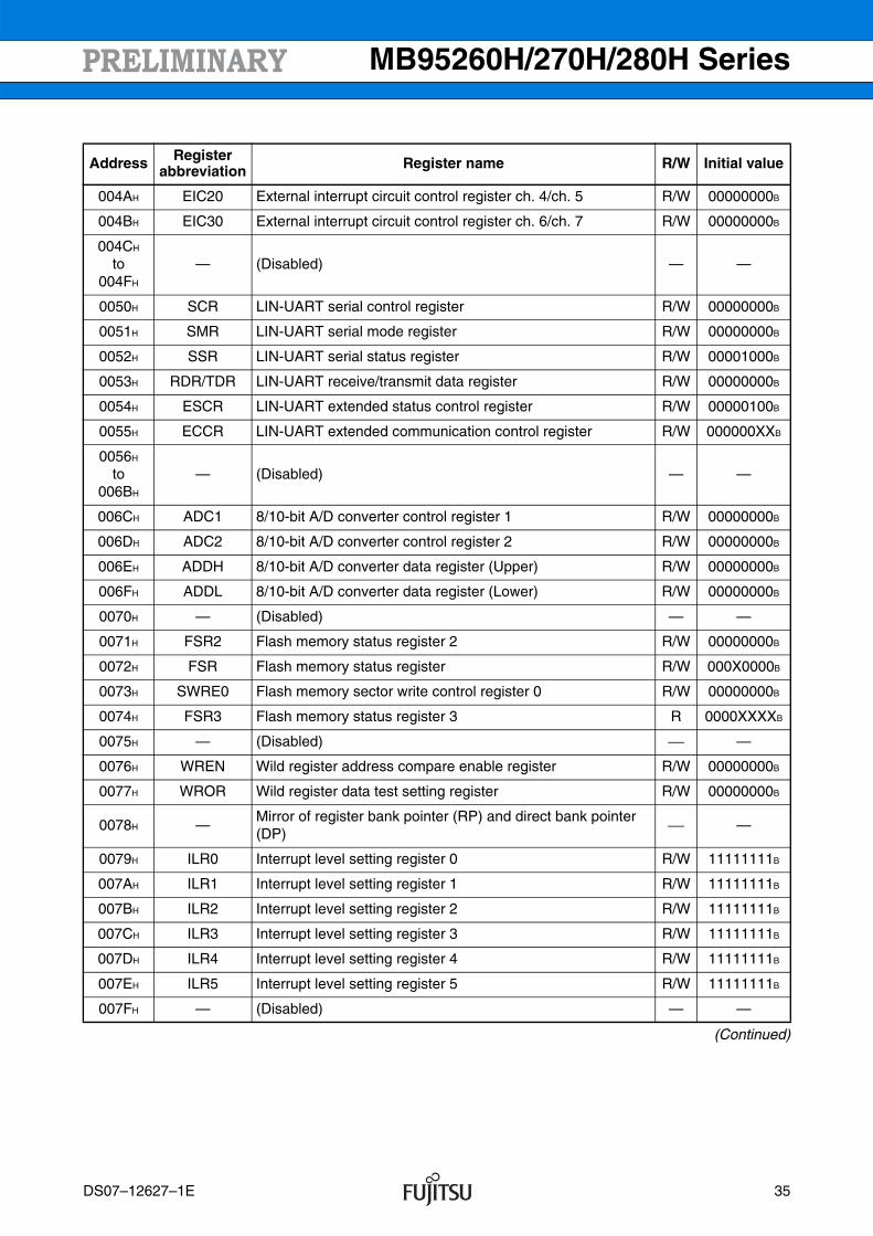
Address Registerabbreviation Register name R/W Initial value
0000H PDR0 Port 0 data register R/W 00000000B
0001H DDR0 Port 0 direction register R/W 00000000B
0002H PDR1 Port 1 data register R/W 00000000B
0003H DDR1 Port 1 direction register R/W 00000000B
0004H — (Disabled) — —
0005H WATR Oscillation stabilization wait time setting register R/W 11111111B
0006H — (Disabled) — —
0007H SYCC System clock control register R/W 0000X011B
0008H STBC Standby control register R/W 00000XXXB
0009H RSRR Reset source register R XXXXXXXXB
000AH TBTC Timebase timer control register R/W 00000000B
000BH WPCR Watch prescaler control register R/W 00000000B
000CH WDTC Watchdog timer control register R/W 00XX0000B
000DH SYCC2 System clock control register 2 R/W XX100011B
000EH
to0015H
— (Disabled) — —
0016H PDR6 Port 6 data register R/W 00000000B
0017H DDR6 Port 6 direction register R/W 00000000B
0018H
to0027H
— (Disabled) — —
0028H PDRF Port F data register R/W 00000000B
0029H DDRF Port F direction register R/W 00000000B
002AH PDRG Port G data register R/W 00000000B
002BH DDRG Port G direction register R/W 00000000B
002CH PUL0 Port 0 pull-up register R/W 00000000B
002DH
to0034H
— (Disabled) — —
0035H PULG Port G pull-up register R/W 00000000B
0036H T01CR1 8/16-bit composite timer 01 status control register 1 ch. 0 R/W 00000000B
0037H T00CR1 8/16-bit composite timer 00 status control register 1 ch. 0 R/W 00000000B
0038H T11CR1 8/16-bit composite timer 11 status control register 1 ch. 1 R/W 00000000B
0039H T10CR1 8/16-bit composite timer 10 status control register 1 ch. 1 R/W 00000000B
003AH
to0048H
— (Disabled) — —
0049H EIC10 External interrupt circuit control register ch. 2/ch. 3 R/W 00000000B
26 DS07–12627–1E
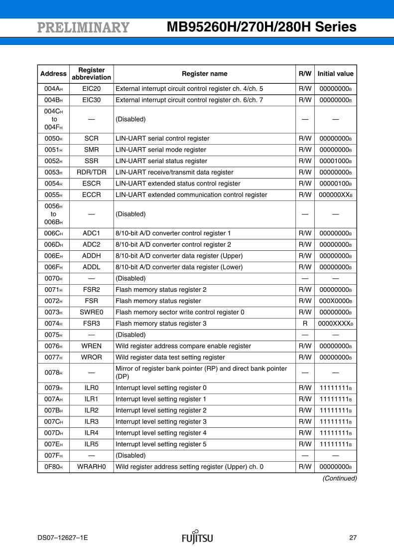
MB95260H/270H/280H Series
(Continued)
Address Registerabbreviation Register name R/W Initial value
004AH EIC20 External interrupt circuit control register ch. 4/ch. 5 R/W 00000000B
004BH EIC30 External interrupt circuit control register ch. 6/ch. 7 R/W 00000000B
004CH
to 004FH
— (Disabled) — —
0050H SCR LIN-UART serial control register R/W 00000000B
0051H SMR LIN-UART serial mode register R/W 00000000B
0052H SSR LIN-UART serial status register R/W 00001000B
0053H RDR/TDR LIN-UART receive/transmit data register R/W 00000000B
0054H ESCR LIN-UART extended status control register R/W 00000100B
0055H ECCR LIN-UART extended communication control register R/W 000000XXB
0056H
to006BH
— (Disabled) — —
006CH ADC1 8/10-bit A/D converter control register 1 R/W 00000000B
006DH ADC2 8/10-bit A/D converter control register 2 R/W 00000000B
006EH ADDH 8/10-bit A/D converter data register (Upper) R/W 00000000B
006FH ADDL 8/10-bit A/D converter data register (Lower) R/W 00000000B
0070H — (Disabled) — —
0071H FSR2 Flash memory status register 2 R/W 00000000B
0072H FSR Flash memory status register R/W 000X0000B
0073H SWRE0 Flash memory sector write control register 0 R/W 00000000B
0074H FSR3 Flash memory status register 3 R 0000XXXXB
0075H — (Disabled) — —
0076H WREN Wild register address compare enable register R/W 00000000B
0077H WROR Wild register data test setting register R/W 00000000B
0078H —Mirror of register bank pointer (RP) and direct bank pointer (DP)
— —
0079H ILR0 Interrupt level setting register 0 R/W 11111111B
007AH ILR1 Interrupt level setting register 1 R/W 11111111B
007BH ILR2 Interrupt level setting register 2 R/W 11111111B
007CH ILR3 Interrupt level setting register 3 R/W 11111111B
007DH ILR4 Interrupt level setting register 4 R/W 11111111B
007EH ILR5 Interrupt level setting register 5 R/W 11111111B
007FH — (Disabled) — —
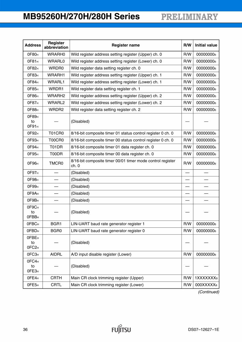
0F80H WRARH0 Wild register address setting register (Upper) ch. 0 R/W 00000000B
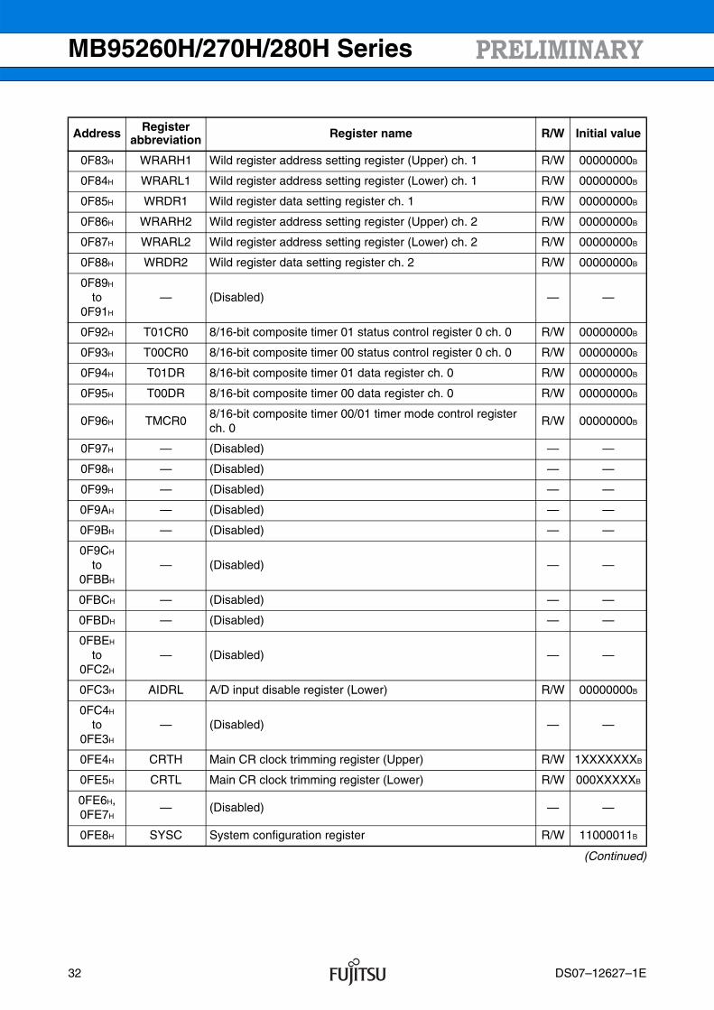
DS07–12627–1E 27
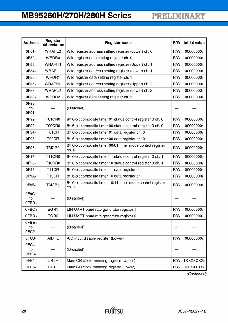
MB95260H/270H/280H Series
(Continued)
Address Registerabbreviation Register name R/W Initial value
0F81H WRARL0 Wild register address setting register (Lower) ch. 0 R/W 00000000B
0F82H WRDR0 Wild register data setting register ch. 0 R/W 00000000B
0F83H WRARH1 Wild register address setting register (Upper) ch. 1 R/W 00000000B
0F84H WRARL1 Wild register address setting register (Lower) ch. 1 R/W 00000000B
0F85H WRDR1 Wild register data setting register ch. 1 R/W 00000000B
0F86H WRARH2 Wild register address setting register (Upper) ch. 2 R/W 00000000B
0F87H WRARL2 Wild register address setting register (Lower) ch. 2 R/W 00000000B
0F88H WRDR2 Wild register data setting register ch. 2 R/W 00000000B
0F89H
to0F91H
— (Disabled) — —
0F92H T01CR0 8/16-bit composite timer 01 status control register 0 ch. 0 R/W 00000000B
0F93H T00CR0 8/16-bit composite timer 00 status control register 0 ch. 0 R/W 00000000B
0F94H T01DR 8/16-bit composite timer 01 data register ch. 0 R/W 00000000B
0F95H T00DR 8/16-bit composite timer 00 data register ch. 0 R/W 00000000B
0F96H TMCR08/16-bit composite timer 00/01 timer mode control register ch. 0
R/W 00000000B
0F97H T11CR0 8/16-bit composite timer 11 status control register 0 ch. 1 R/W 00000000B
0F98H T10CR0 8/16-bit composite timer 10 status control register 0 ch. 1 R/W 00000000B
0F99H T11DR 8/16-bit composite timer 11 data register ch. 1 R/W 00000000B
0F9AH T10DR 8/16-bit composite timer 10 data register ch. 1 R/W 00000000B
0F9BH TMCR18/16-bit composite timer 10/11 timer mode control register ch. 1
R/W 00000000B
0F9CH
to0FBBH
— (Disabled) — —
0FBCH BGR1 LIN-UART baud rate generator register 1 R/W 00000000B
0FBDH BGR0 LIN-UART baud rate generator register 0 R/W 00000000B
0FBEH
to0FC2H
— (Disabled) — —
0FC3H AIDRL A/D input disable register (Lower) R/W 00000000B
0FC4H
to0FE3H
— (Disabled) — —
0FE4H CRTH Main CR clock trimming register (Upper) R/W 1XXXXXXXB
0FE5H CRTL Main CR clock trimming register (Lower) R/W 000XXXXXB
28 DS07–12627–1E

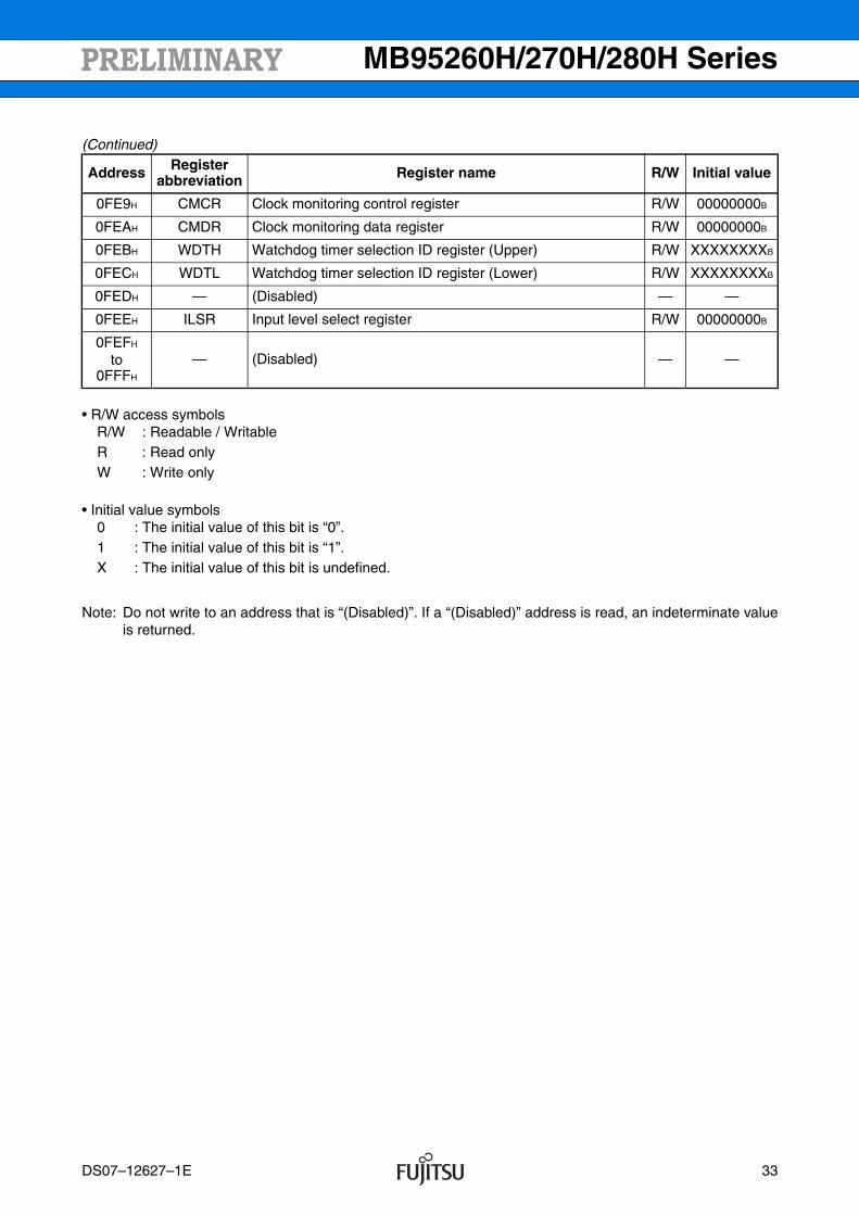
MB95260H/270H/280H Series
(Continued)
• R/W access symbols
• Initial value symbols
Note: Do not write to an address that is “(Disabled)”. If a “(Disabled)” address is read, an indeterminate valueis returned.
Address Registerabbreviation Register name R/W Initial value
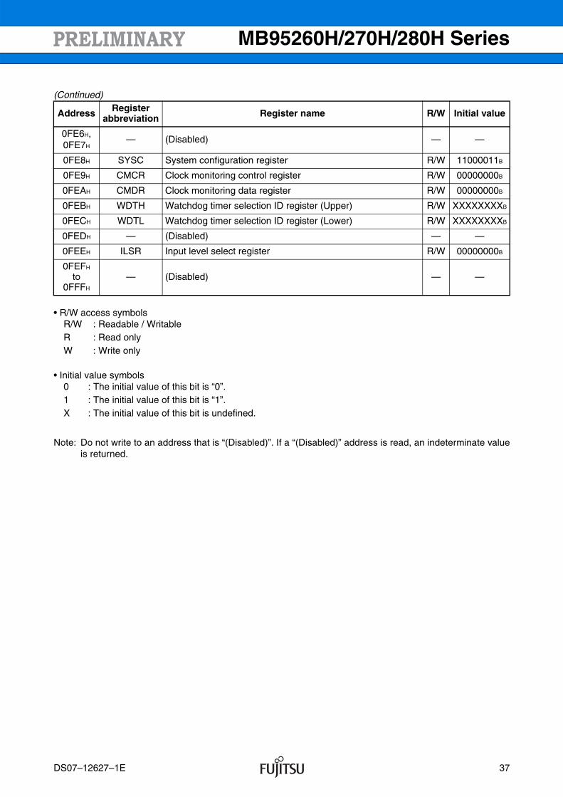
0FE6H, 0FE7H
— (Disabled) — —
0FE8H SYSC System configuration register R/W 11000011B
0FE9H CMCR Clock monitoring control register R/W 00000000B
0FEAH CMDR Clock monitoring data register R/W 00000000B
0FEBH WDTH Watchdog timer selection ID register (Upper) R/W XXXXXXXXB
0FECH WDTL Watchdog timer selection ID register (Lower) R/W XXXXXXXXB
0FEDH — (Disabled) — —
0FEEH ILSR Input level select register R/W 00000000B
0FEFH
to0FFFH
— (Disabled) — —
R/W : Readable / WritableR : Read onlyW : Write only
0 : The initial value of this bit is “0”.1 : The initial value of this bit is “1”.X : The initial value of this bit is undefined.
DS07–12627–1E 29
MB95260H/270H/280H Series
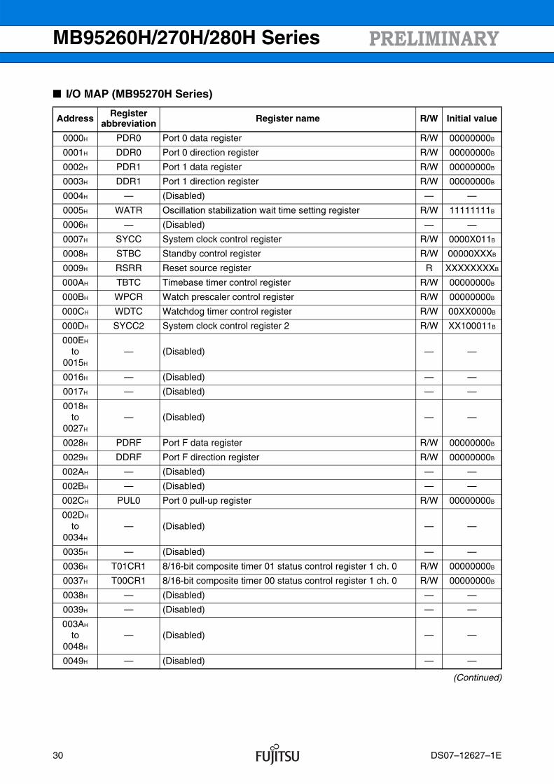
I/O MAP (MB95270H Series)
(Continued)
Address Registerabbreviation Register name R/W Initial value
0000H PDR0 Port 0 data register R/W 00000000B
0001H DDR0 Port 0 direction register R/W 00000000B
0002H PDR1 Port 1 data register R/W 00000000B
0003H DDR1 Port 1 direction register R/W 00000000B
0004H — (Disabled) — —
0005H WATR Oscillation stabilization wait time setting register R/W 11111111B
0006H — (Disabled) — —
0007H SYCC System clock control register R/W 0000X011B
0008H STBC Standby control register R/W 00000XXXB
0009H RSRR Reset source register R XXXXXXXXB
000AH TBTC Timebase timer control register R/W 00000000B
000BH WPCR Watch prescaler control register R/W 00000000B
000CH WDTC Watchdog timer control register R/W 00XX0000B
000DH SYCC2 System clock control register 2 R/W XX100011B
000EH
to0015H
— (Disabled) — —
0016H — (Disabled) — —
0017H — (Disabled) — —
0018H
to0027H
— (Disabled) — —
0028H PDRF Port F data register R/W 00000000B
0029H DDRF Port F direction register R/W 00000000B
002AH — (Disabled) — —
002BH — (Disabled) — —
002CH PUL0 Port 0 pull-up register R/W 00000000B
002DH
to0034H
— (Disabled) — —
0035H — (Disabled) — —
0036H T01CR1 8/16-bit composite timer 01 status control register 1 ch. 0 R/W 00000000B
0037H T00CR1 8/16-bit composite timer 00 status control register 1 ch. 0 R/W 00000000B
0038H — (Disabled) — —
0039H — (Disabled) — —
003AH
to0048H
— (Disabled) — —
0049H — (Disabled) — —
30 DS07–12627–1E
MB95260H/270H/280H Series
(Continued)
Address Registerabbreviation Register name R/W Initial value
004AH EIC20 External interrupt circuit control register ch. 4 R/W 00000000B
004BH EIC30 External interrupt circuit control register ch. 6 R/W 00000000B
004CH
to004FH
— (Disabled) — —
0050H — (Disabled) — —
0051H — (Disabled) — —
0052H — (Disabled) — —
0053H — (Disabled) — —
0054H — (Disabled) — —
0055H — (Disabled) — —
0056H
to006BH
— (Disabled) — —
006CH ADC1 8/10-bit A/D converter control register 1 R/W 00000000B
006DH ADC2 8/10-bit A/D converter control register 2 R/W 00000000B
006EH ADDH 8/10-bit A/D converter data register (Upper) R/W 00000000B
006FH ADDL 8/10-bit A/D converter data register (Lower) R/W 00000000B
0070H — (Disabled) — —
0071H FSR2 Flash memory status register 2 R/W 00000000B
0072H FSR Flash memory status register R/W 000X0000B
0073H SWRE0 Flash memory sector write control register 0 R/W 00000000B
0074H FSR3 Flash memory status register 3 R 0000XXXXB
0075H — (Disabled) — —
0076H WREN Wild register address compare enable register R/W 00000000B
0077H WROR Wild register data test setting register R/W 00000000B
0078H —Mirror of register bank pointer (RP) and direct bank pointer (DP)
— —
0079H ILR0 Interrupt level setting register 0 R/W 11111111B
007AH ILR1 Interrupt level setting register 1 R/W 11111111B
007BH — (Disabled) — —
007CH — (Disabled) — —
007DH ILR4 Interrupt level setting register 4 R/W 11111111B
007EH ILR5 Interrupt level setting register 5 R/W 11111111B
007FH — (Disabled) — —
0F80H WRARH0 Wild register address setting register (Upper) ch. 0 R/W 00000000B
0F81H WRARL0 Wild register address setting register (Lower) ch. 0 R/W 00000000B
0F82H WRDR0 Wild register data setting register ch. 0 R/W 00000000B
DS07–12627–1E 31
MB95260H/270H/280H Series
(Continued)
Address Registerabbreviation Register name R/W Initial value
0F83H WRARH1 Wild register address setting register (Upper) ch. 1 R/W 00000000B
0F84H WRARL1 Wild register address setting register (Lower) ch. 1 R/W 00000000B
0F85H WRDR1 Wild register data setting register ch. 1 R/W 00000000B
0F86H WRARH2 Wild register address setting register (Upper) ch. 2 R/W 00000000B
0F87H WRARL2 Wild register address setting register (Lower) ch. 2 R/W 00000000B
0F88H WRDR2 Wild register data setting register ch. 2 R/W 00000000B
0F89H
to0F91H
— (Disabled) — —
0F92H T01CR0 8/16-bit composite timer 01 status control register 0 ch. 0 R/W 00000000B
0F93H T00CR0 8/16-bit composite timer 00 status control register 0 ch. 0 R/W 00000000B
0F94H T01DR 8/16-bit composite timer 01 data register ch. 0 R/W 00000000B
0F95H T00DR 8/16-bit composite timer 00 data register ch. 0 R/W 00000000B
0F96H TMCR08/16-bit composite timer 00/01 timer mode control register ch. 0
R/W 00000000B
0F97H — (Disabled) — —
0F98H — (Disabled) — —
0F99H — (Disabled) — —
0F9AH — (Disabled) — —
0F9BH — (Disabled) — —
0F9CH
to0FBBH
— (Disabled) — —
0FBCH — (Disabled) — —
0FBDH — (Disabled) — —
0FBEH
to0FC2H
— (Disabled) — —
0FC3H AIDRL A/D input disable register (Lower) R/W 00000000B
0FC4H
to0FE3H
— (Disabled) — —
0FE4H CRTH Main CR clock trimming register (Upper) R/W 1XXXXXXXB
0FE5H CRTL Main CR clock trimming register (Lower) R/W 000XXXXXB
0FE6H, 0FE7H
— (Disabled) — —
0FE8H SYSC System configuration register R/W 11000011B
32 DS07–12627–1E
MB95260H/270H/280H Series
(Continued)
• R/W access symbols
• Initial value symbols
Note: Do not write to an address that is “(Disabled)”. If a “(Disabled)” address is read, an indeterminate valueis returned.
Address Registerabbreviation Register name R/W Initial value
0FE9H CMCR Clock monitoring control register R/W 00000000B
0FEAH CMDR Clock monitoring data register R/W 00000000B
0FEBH WDTH Watchdog timer selection ID register (Upper) R/W XXXXXXXXB
0FECH WDTL Watchdog timer selection ID register (Lower) R/W XXXXXXXXB
0FEDH — (Disabled) — —
0FEEH ILSR Input level select register R/W 00000000B
0FEFH
to0FFFH
— (Disabled) — —
R/W : Readable / WritableR : Read onlyW : Write only
0 : The initial value of this bit is “0”.1 : The initial value of this bit is “1”.X : The initial value of this bit is undefined.
DS07–12627–1E 33
MB95260H/270H/280H Series
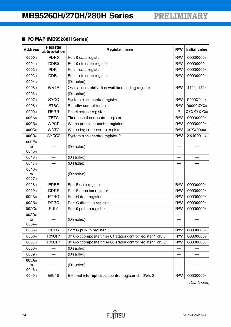
I/O MAP (MB95280H Series)
(Continued)
Address Registerabbreviation Register name R/W Initial value
0000H PDR0 Port 0 data register R/W 00000000B
0001H DDR0 Port 0 direction register R/W 00000000B
0002H PDR1 Port 1 data register R/W 00000000B
0003H DDR1 Port 1 direction register R/W 00000000B
0004H — (Disabled) — —
0005H WATR Oscillation stabilization wait time setting register R/W 11111111B
0006H — (Disabled) — —
0007H SYCC System clock control register R/W 0000X011B
0008H STBC Standby control register R/W 00000XXXB
0009H RSRR Reset source register R XXXXXXXXB
000AH TBTC Timebase timer control register R/W 00000000B
000BH WPCR Watch prescaler control register R/W 00000000B
000CH WDTC Watchdog timer control register R/W 00XX0000B
000DH SYCC2 System clock control register 2 R/W XX100011B
000EH
to0015H
— (Disabled) — —
0016H — (Disabled) — —
0017H — (Disabled) — —
0018H
to0027H
— (Disabled) — —
0028H PDRF Port F data register R/W 00000000B
0029H DDRF Port F direction register R/W 00000000B
002AH PDRG Port G data register R/W 00000000B
002BH DDRG Port G direction register R/W 00000000B
002CH PUL0 Port 0 pull-up register R/W 00000000B
002DH
to0034H
— (Disabled) — —
0035H PULG Port G pull-up register R/W 00000000B
0036H T01CR1 8/16-bit composite timer 01 status control register 1 ch. 0 R/W 00000000B
0037H T00CR1 8/16-bit composite timer 00 status control register 1 ch. 0 R/W 00000000B
0038H — (Disabled) — —
0039H — (Disabled) — —
003AH
to0048H
— (Disabled) — —
0049H EIC10 External interrupt circuit control register ch. 2/ch. 3 R/W 00000000B
34 DS07–12627–1E
MB95260H/270H/280H Series
(Continued)
Address Registerabbreviation Register name R/W Initial value
004AH EIC20 External interrupt circuit control register ch. 4/ch. 5 R/W 00000000B
004BH EIC30 External interrupt circuit control register ch. 6/ch. 7 R/W 00000000B
004CH
to004FH
— (Disabled) — —
0050H SCR LIN-UART serial control register R/W 00000000B
0051H SMR LIN-UART serial mode register R/W 00000000B
0052H SSR LIN-UART serial status register R/W 00001000B
0053H RDR/TDR LIN-UART receive/transmit data register R/W 00000000B
0054H ESCR LIN-UART extended status control register R/W 00000100B
0055H ECCR LIN-UART extended communication control register R/W 000000XXB
0056H
to006BH
— (Disabled) — —
006CH ADC1 8/10-bit A/D converter control register 1 R/W 00000000B
006DH ADC2 8/10-bit A/D converter control register 2 R/W 00000000B
006EH ADDH 8/10-bit A/D converter data register (Upper) R/W 00000000B
006FH ADDL 8/10-bit A/D converter data register (Lower) R/W 00000000B
0070H — (Disabled) — —
0071H FSR2 Flash memory status register 2 R/W 00000000B
0072H FSR Flash memory status register R/W 000X0000B
0073H SWRE0 Flash memory sector write control register 0 R/W 00000000B
0074H FSR3 Flash memory status register 3 R 0000XXXXB
0075H — (Disabled) ⎯ —
0076H WREN Wild register address compare enable register R/W 00000000B
0077H WROR Wild register data test setting register R/W 00000000B
0078H —Mirror of register bank pointer (RP) and direct bank pointer (DP)
⎯ —
0079H ILR0 Interrupt level setting register 0 R/W 11111111B
007AH ILR1 Interrupt level setting register 1 R/W 11111111B
007BH ILR2 Interrupt level setting register 2 R/W 11111111B
007CH ILR3 Interrupt level setting register 3 R/W 11111111B
007DH ILR4 Interrupt level setting register 4 R/W 11111111B
007EH ILR5 Interrupt level setting register 5 R/W 11111111B
007FH — (Disabled) — —
DS07–12627–1E 35
MB95260H/270H/280H Series
(Continued)
Address Registerabbreviation Register name R/W Initial value
0F80H WRARH0 Wild register address setting register (Upper) ch. 0 R/W 00000000B
0F81H WRARL0 Wild register address setting register (Lower) ch. 0 R/W 00000000B
0F82H WRDR0 Wild register data setting register ch. 0 R/W 00000000B
0F83H WRARH1 Wild register address setting register (Upper) ch. 1 R/W 00000000B
0F84H WRARL1 Wild register address setting register (Lower) ch. 1 R/W 00000000B
0F85H WRDR1 Wild register data setting register ch. 1 R/W 00000000B
0F86H WRARH2 Wild register address setting register (Upper) ch. 2 R/W 00000000B
0F87H WRARL2 Wild register address setting register (Lower) ch. 2 R/W 00000000B
0F88H WRDR2 Wild register data setting register ch. 2 R/W 00000000B
0F89H
to0F91H
— (Disabled) — —
0F92H T01CR0 8/16-bit composite timer 01 status control register 0 ch. 0 R/W 00000000B
0F93H T00CR0 8/16-bit composite timer 00 status control register 0 ch. 0 R/W 00000000B
0F94H T01DR 8/16-bit composite timer 01 data register ch. 0 R/W 00000000B
0F95H T00DR 8/16-bit composite timer 00 data register ch. 0 R/W 00000000B
0F96H TMCR08/16-bit composite timer 00/01 timer mode control register ch. 0
R/W 00000000B
0F97H — (Disabled) — —
0F98H — (Disabled) — —
0F99H — (Disabled) — —
0F9AH — (Disabled) — —
0F9BH — (Disabled) — —
0F9CH
to0FBBH
— (Disabled) — —
0FBCH BGR1 LIN-UART baud rate generator register 1 R/W 00000000B
0FBDH BGR0 LIN-UART baud rate generator register 0 R/W 00000000B
0FBEH
to0FC2H
— (Disabled) — —
0FC3H AIDRL A/D input disable register (Lower) R/W 00000000B
0FC4H
to0FE3H
— (Disabled) — —
0FE4H CRTH Main CR clock trimming register (Upper) R/W 1XXXXXXXB
0FE5H CRTL Main CR clock trimming register (Lower) R/W 000XXXXXB
36 DS07–12627–1E
MB95260H/270H/280H Series
(Continued)
• R/W access symbols
• Initial value symbols
Note: Do not write to an address that is “(Disabled)”. If a “(Disabled)” address is read, an indeterminate valueis returned.
Address Registerabbreviation Register name R/W Initial value
0FE6H, 0FE7H
— (Disabled) — —
0FE8H SYSC System configuration register R/W 11000011B
0FE9H CMCR Clock monitoring control register R/W 00000000B
0FEAH CMDR Clock monitoring data register R/W 00000000B
0FEBH WDTH Watchdog timer selection ID register (Upper) R/W XXXXXXXXB
0FECH WDTL Watchdog timer selection ID register (Lower) R/W XXXXXXXXB
0FEDH — (Disabled) — —
0FEEH ILSR Input level select register R/W 00000000B
0FEFH
to0FFFH
— (Disabled) — —
R/W : Readable / WritableR : Read onlyW : Write only
0 : The initial value of this bit is “0”.1 : The initial value of this bit is “1”.X : The initial value of this bit is undefined.
DS07–12627–1E 37
MB95260H/270H/280H Series
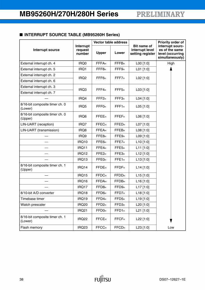
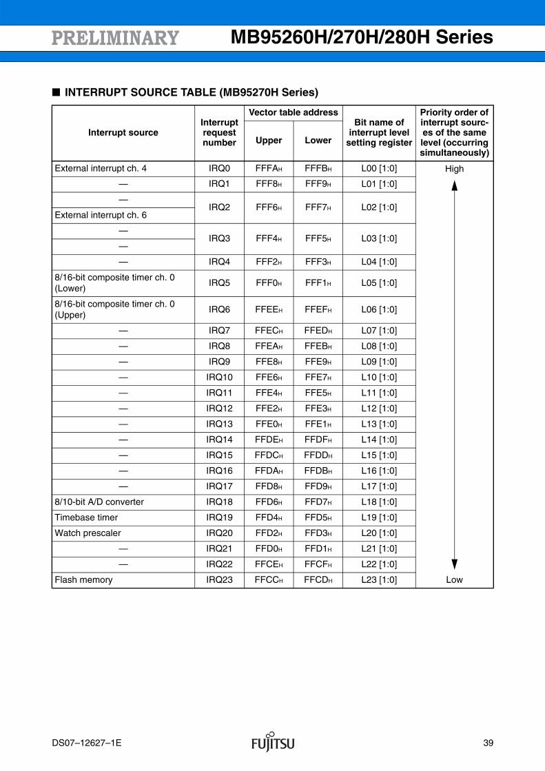
INTERRUPT SOURCE TABLE (MB95260H Series)
Interrupt sourceInterrupt request number
Vector table addressBit name of
interrupt level setting register
Priority order of interrupt sourc-es of the same level (occurring simultaneously)
Upper Lower
External interrupt ch. 4 IRQ0 FFFAH FFFBH L00 [1:0] High
External interrupt ch. 5 IRQ1 FFF8H FFF9H L01 [1:0]
External interrupt ch. 2IRQ2 FFF6H FFF7H L02 [1:0]
External interrupt ch. 6
External interrupt ch. 3IRQ3 FFF4H FFF5H L03 [1:0]
External interrupt ch. 7
— IRQ4 FFF2H FFF3H L04 [1:0]
8/16-bit composite timer ch. 0 (Lower)
IRQ5 FFF0H FFF1H L05 [1:0]
8/16-bit composite timer ch. 0 (Upper)
IRQ6 FFEEH FFEFH L06 [1:0]
LIN-UART (reception) IRQ7 FFECH FFEDH L07 [1:0]
LIN-UART (transmission) IRQ8 FFEAH FFEBH L08 [1:0]
— IRQ9 FFE8H FFE9H L09 [1:0]
— IRQ10 FFE6H FFE7H L10 [1:0]
— IRQ11 FFE4H FFE5H L11 [1:0]
— IRQ12 FFE2H FFE3H L12 [1:0]
— IRQ13 FFE0H FFE1H L13 [1:0]
8/16-bit composite timer ch. 1 (Upper)
IRQ14 FFDEH FFDFH L14 [1:0]
— IRQ15 FFDCH FFDDH L15 [1:0]
— IRQ16 FFDAH FFDBH L16 [1:0]
— IRQ17 FFD8H FFD9H L17 [1:0]
8/10-bit A/D converter IRQ18 FFD6H FFD7H L18 [1:0]
Timebase timer IRQ19 FFD4H FFD5H L19 [1:0]
Watch prescaler IRQ20 FFD2H FFD3H L20 [1:0]
— IRQ21 FFD0H FFD1H L21 [1:0]
8/16-bit composite timer ch. 1 (Lower)
IRQ22 FFCEH FFCFH L22 [1:0]
Flash memory IRQ23 FFCCH FFCDH L23 [1:0] Low
38 DS07–12627–1E
MB95260H/270H/280H Series
INTERRUPT SOURCE TABLE (MB95270H Series)
Interrupt sourceInterrupt request number
Vector table addressBit name of
interrupt level setting register
Priority order of interrupt sourc-es of the same level (occurring simultaneously)
Upper Lower
External interrupt ch. 4 IRQ0 FFFAH FFFBH L00 [1:0] High
— IRQ1 FFF8H FFF9H L01 [1:0]
—IRQ2 FFF6H FFF7H L02 [1:0]
External interrupt ch. 6
—IRQ3 FFF4H FFF5H L03 [1:0]
—
— IRQ4 FFF2H FFF3H L04 [1:0]
8/16-bit composite timer ch. 0 (Lower)
IRQ5 FFF0H FFF1H L05 [1:0]
8/16-bit composite timer ch. 0 (Upper)
IRQ6 FFEEH FFEFH L06 [1:0]
— IRQ7 FFECH FFEDH L07 [1:0]
— IRQ8 FFEAH FFEBH L08 [1:0]
— IRQ9 FFE8H FFE9H L09 [1:0]
— IRQ10 FFE6H FFE7H L10 [1:0]
— IRQ11 FFE4H FFE5H L11 [1:0]
— IRQ12 FFE2H FFE3H L12 [1:0]
— IRQ13 FFE0H FFE1H L13 [1:0]
— IRQ14 FFDEH FFDFH L14 [1:0]
— IRQ15 FFDCH FFDDH L15 [1:0]
— IRQ16 FFDAH FFDBH L16 [1:0]
— IRQ17 FFD8H FFD9H L17 [1:0]
8/10-bit A/D converter IRQ18 FFD6H FFD7H L18 [1:0]
Timebase timer IRQ19 FFD4H FFD5H L19 [1:0]
Watch prescaler IRQ20 FFD2H FFD3H L20 [1:0]
— IRQ21 FFD0H FFD1H L21 [1:0]
— IRQ22 FFCEH FFCFH L22 [1:0]
Flash memory IRQ23 FFCCH FFCDH L23 [1:0] Low
DS07–12627–1E 39
MB95260H/270H/280H Series
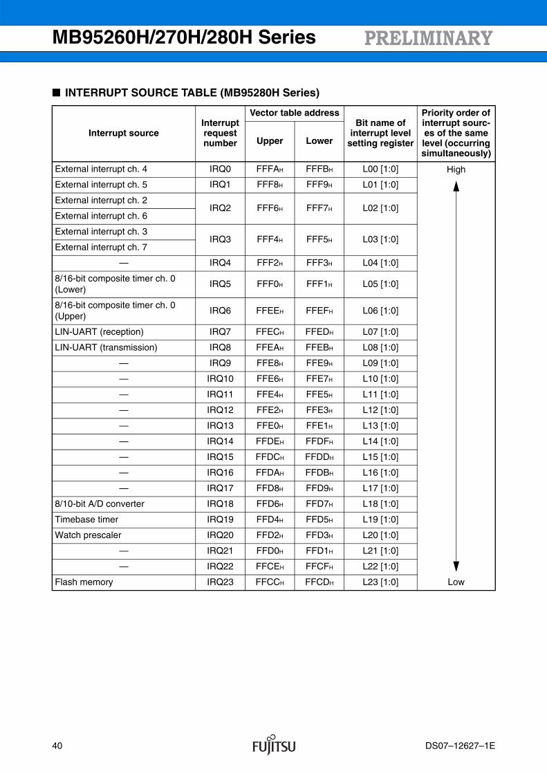
INTERRUPT SOURCE TABLE (MB95280H Series)
Interrupt sourceInterrupt request number
Vector table addressBit name of
interrupt level setting register
Priority order of interrupt sourc-es of the same level (occurring simultaneously)
Upper Lower
External interrupt ch. 4 IRQ0 FFFAH FFFBH L00 [1:0] High
External interrupt ch. 5 IRQ1 FFF8H FFF9H L01 [1:0]
External interrupt ch. 2IRQ2 FFF6H FFF7H L02 [1:0]
External interrupt ch. 6
External interrupt ch. 3IRQ3 FFF4H FFF5H L03 [1:0]
External interrupt ch. 7
— IRQ4 FFF2H FFF3H L04 [1:0]
8/16-bit composite timer ch. 0 (Lower)
IRQ5 FFF0H FFF1H L05 [1:0]
8/16-bit composite timer ch. 0 (Upper)
IRQ6 FFEEH FFEFH L06 [1:0]
LIN-UART (reception) IRQ7 FFECH FFEDH L07 [1:0]
LIN-UART (transmission) IRQ8 FFEAH FFEBH L08 [1:0]
— IRQ9 FFE8H FFE9H L09 [1:0]
— IRQ10 FFE6H FFE7H L10 [1:0]
— IRQ11 FFE4H FFE5H L11 [1:0]
— IRQ12 FFE2H FFE3H L12 [1:0]
— IRQ13 FFE0H FFE1H L13 [1:0]
— IRQ14 FFDEH FFDFH L14 [1:0]
— IRQ15 FFDCH FFDDH L15 [1:0]
— IRQ16 FFDAH FFDBH L16 [1:0]
— IRQ17 FFD8H FFD9H L17 [1:0]
8/10-bit A/D converter IRQ18 FFD6H FFD7H L18 [1:0]
Timebase timer IRQ19 FFD4H FFD5H L19 [1:0]
Watch prescaler IRQ20 FFD2H FFD3H L20 [1:0]
— IRQ21 FFD0H FFD1H L21 [1:0]
— IRQ22 FFCEH FFCFH L22 [1:0]
Flash memory IRQ23 FFCCH FFCDH L23 [1:0] Low
40 DS07–12627–1E
MB95260H/270H/280H Series
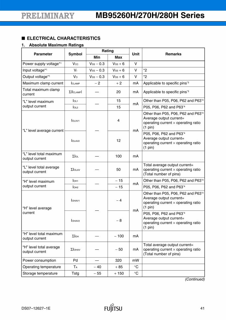
ELECTRICAL CHARACTERISTICS1. Absolute Maximum Ratings
(Continued)
Parameter SymbolRating
Unit RemarksMin Max
Power supply voltage*1 VCC VSS − 0.3 VSS + 6 V
Input voltage*1 VI VSS − 0.3 VSS + 6 V *2
Output voltage*1 VO VSS − 0.3 VSS + 6 V *2
Maximum clamp current ICLAMP − 2 + 2 mA Applicable to specific pins*3
Total maximum clamp current
Σ|ICLAMP| — 20 mA Applicable to specific pins*3
“L” level maximum output current
IOL1—
15mA
Other than P05, P06, P62 and P63*4
IOL2 15 P05, P06, P62 and P63*4
“L” level average current
IOLAV1
—
4
mA
Other than P05, P06, P62 and P63*4
Average output current=operating current × operating ratio(1 pin)
IOLAV2 12
P05, P06, P62 and P63*4
Average output current=operating current × operating ratio(1 pin)
“L” level total maximum output current
ΣIOL — 100 mA
“L” level total average output current
ΣIOLAV — 50 mATotal average output current=operating current × operating ratio(Total number of pins)
“H” level maximum output current
IOH1—
− 15mA
Other than P05, P06, P62 and P63*4
IOH2 − 15 P05, P06, P62 and P63*4
“H” level average current
IOHAV1
—
− 4
mA
Other than P05, P06, P62 and P63*4
Average output current=operating current × operating ratio(1 pin)
IOHAV2 − 8
P05, P06, P62 and P63*4
Average output current=operating current × operating ratio(1 pin)
“H” level total maximum output current
ΣIOH — − 100 mA
“H” level total average output current
ΣIOHAV — − 50 mATotal average output current=operating current × operating ratio(Total number of pins)
Power consumption Pd — 320 mW
Operating temperature TA − 40 + 85 °C
Storage temperature Tstg − 55 + 150 °C
DS07–12627–1E 41
MB95260H/270H/280H Series
(Continued)
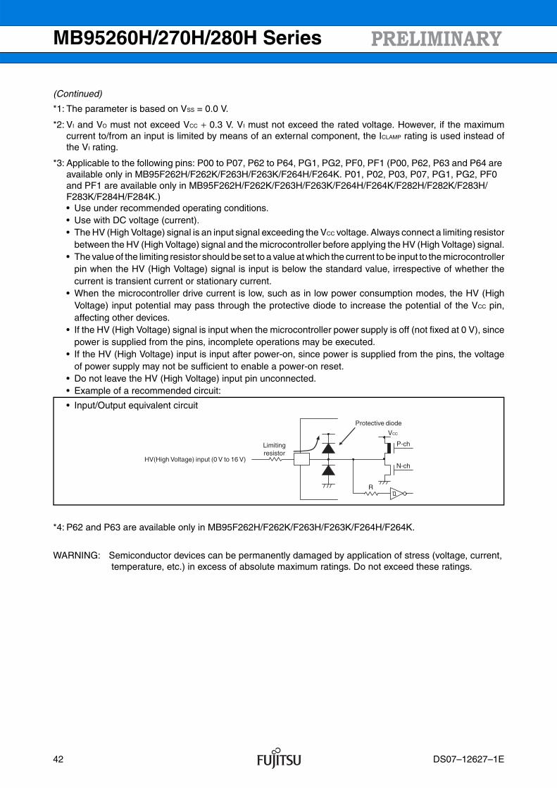
*1: The parameter is based on VSS = 0.0 V.
*2: VI and VO must not exceed VCC + 0.3 V. VI must not exceed the rated voltage. However, if the maximumcurrent to/from an input is limited by means of an external component, the ICLAMP rating is used instead ofthe VI rating.
*3: Applicable to the following pins: P00 to P07, P62 to P64, PG1, PG2, PF0, PF1 (P00, P62, P63 and P64 are available only in MB95F262H/F262K/F263H/F263K/F264H/F264K. P01, P02, P03, P07, PG1, PG2, PF0 and PF1 are available only in MB95F262H/F262K/F263H/F263K/F264H/F264K/F282H/F282K/F283H/F283K/F284H/F284K.)• Use under recommended operating conditions.• Use with DC voltage (current).• The HV (High Voltage) signal is an input signal exceeding the VCC voltage. Always connect a limiting resistor
between the HV (High Voltage) signal and the microcontroller before applying the HV (High Voltage) signal.• The value of the limiting resistor should be set to a value at which the current to be input to the microcontroller
pin when the HV (High Voltage) signal is input is below the standard value, irrespective of whether thecurrent is transient current or stationary current.
• When the microcontroller drive current is low, such as in low power consumption modes, the HV (HighVoltage) input potential may pass through the protective diode to increase the potential of the VCC pin,affecting other devices.
• If the HV (High Voltage) signal is input when the microcontroller power supply is off (not fixed at 0 V), sincepower is supplied from the pins, incomplete operations may be executed.
• If the HV (High Voltage) input is input after power-on, since power is supplied from the pins, the voltageof power supply may not be sufficient to enable a power-on reset.
• Do not leave the HV (High Voltage) input pin unconnected.• Example of a recommended circuit:
*4: P62 and P63 are available only in MB95F262H/F262K/F263H/F263K/F264H/F264K.
WARNING: Semiconductor devices can be permanently damaged by application of stress (voltage, current, temperature, etc.) in excess of absolute maximum ratings. Do not exceed these ratings.
HV(High Voltage) input (0 V to 16 V)
Protective diode
VCC
N-ch
P-ch
R
Limitingresistor
• Input/Output equivalent circuit
42 DS07–12627–1E
MB95260H/270H/280H Series
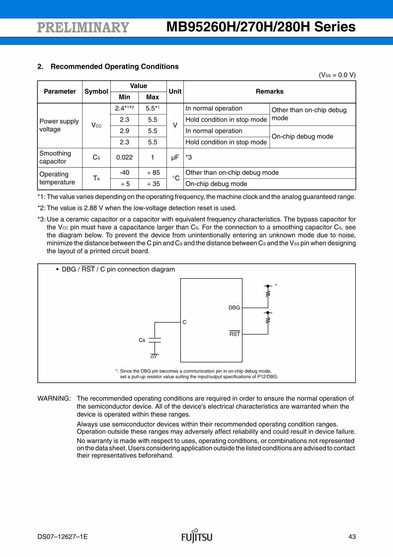
2. Recommended Operating Conditions (VSS = 0.0 V)
*1: The value varies depending on the operating frequency, the machine clock and the analog guaranteed range.
*2: The value is 2.88 V when the low-voltage detection reset is used.
*3: Use a ceramic capacitor or a capacitor with equivalent frequency characteristics. The bypass capacitor forthe VCC pin must have a capacitance larger than CS. For the connection to a smoothing capacitor CS, seethe diagram below. To prevent the device from unintentionally entering an unknown mode due to noise,minimize the distance between the C pin and CS and the distance between CS and the VSS pin when designingthe layout of a printed circuit board.
WARNING: The recommended operating conditions are required in order to ensure the normal operation of the semiconductor device. All of the device's electrical characteristics are warranted when the device is operated within these ranges.
Always use semiconductor devices within their recommended operating condition ranges. Operation outside these ranges may adversely affect reliability and could result in device failure.No warranty is made with respect to uses, operating conditions, or combinations not represented on the data sheet. Users considering application outside the listed conditions are advised to contact their representatives beforehand.
Parameter SymbolValue
Unit RemarksMin Max
Power supply voltage
VCC
2.4*1*2 5.5*1
V
In normal operation Other than on-chip debug mode2.3 5.5 Hold condition in stop mode
2.9 5.5 In normal operationOn-chip debug mode
2.3 5.5 Hold condition in stop mode
Smoothing capacitor
CS 0.022 1 µF *3
Operating temperature
TA-40 + 85
°COther than on-chip debug mode
+ 5 + 35 On-chip debug mode
C
Cs
DBG
*
Since the DBG pin becomes a communication pin in on-chip debug mode,set a pull-up resistor value suiting the input/output specifications of P12/DBG.
*:
RST
• DBG / RST / C pin connection diagram
DS07–12627–1E 43
MB95260H/270H/280H Series
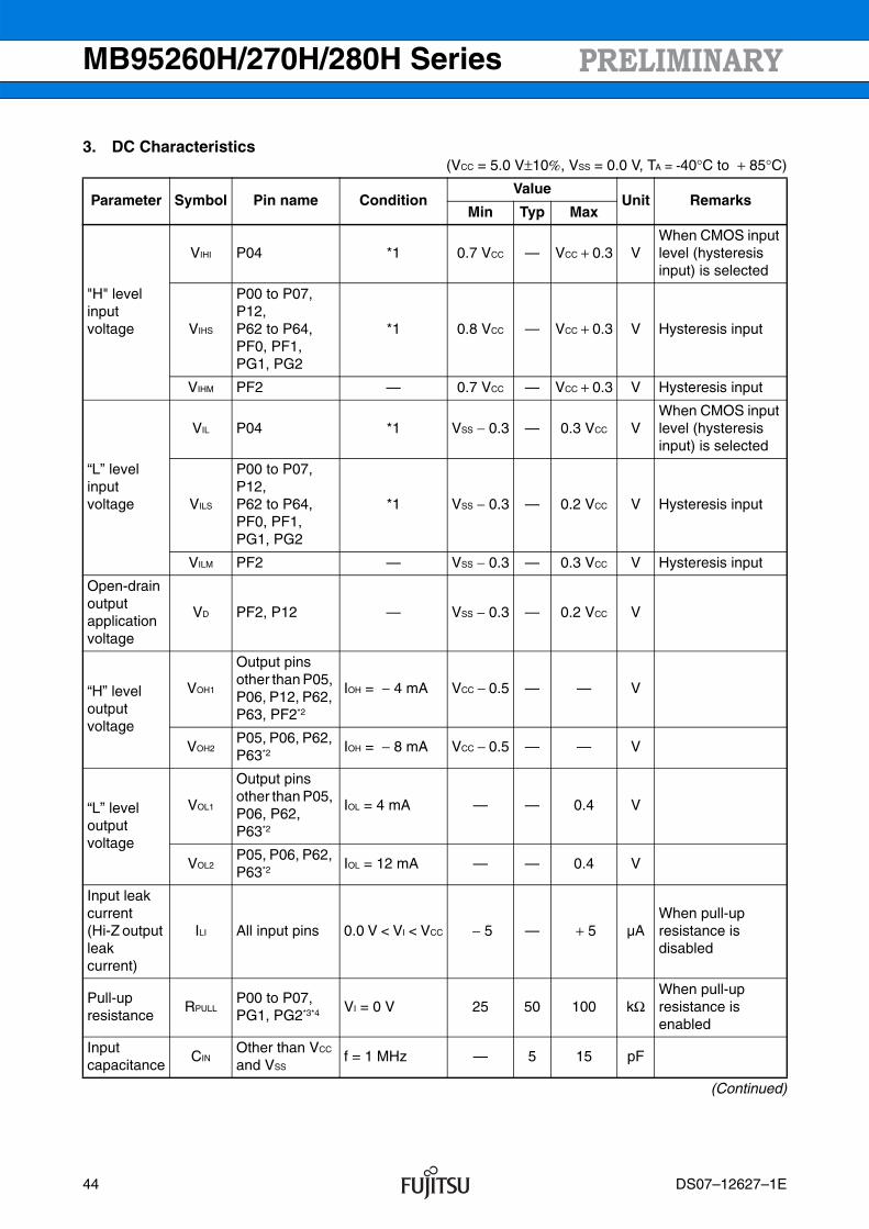
3. DC Characteristics (VCC = 5.0 V±10%, VSS = 0.0 V, TA = -40°C to + 85°C)
(Continued)
Parameter Symbol Pin name ConditionValue
Unit RemarksMin Typ Max
"H" level input voltage
VIHI P04 *1 0.7 VCC — VCC + 0.3 VWhen CMOS input level (hysteresis input) is selected
VIHS
P00 to P07, P12,P62 to P64,PF0, PF1,PG1, PG2
*1 0.8 VCC — VCC + 0.3 V Hysteresis input
VIHM PF2 — 0.7 VCC — VCC + 0.3 V Hysteresis input
“L” level input voltage
VIL P04 *1 VSS − 0.3 — 0.3 VCC VWhen CMOS input level (hysteresis input) is selected
VILS
P00 to P07, P12,P62 to P64,PF0, PF1,PG1, PG2
*1 VSS − 0.3 — 0.2 VCC V Hysteresis input
VILM PF2 — VSS − 0.3 — 0.3 VCC V Hysteresis input
Open-drain output application voltage
VD PF2, P12 — VSS − 0.3 — 0.2 VCC V
“H” level output voltage
VOH1
Output pins other than P05, P06, P12, P62, P63, PF2*2
IOH = − 4 mA VCC − 0.5 — — V
VOH2P05, P06, P62, P63*2 IOH = − 8 mA VCC − 0.5 — — V
“L” level output voltage
VOL1
Output pins other than P05, P06, P62, P63*2
IOL = 4 mA — — 0.4 V
VOL2P05, P06, P62, P63*2 IOL = 12 mA — — 0.4 V
Input leak current (Hi-Z output leak current)
ILI All input pins 0.0 V < VI < VCC − 5 — + 5 µAWhen pull-up resistance is disabled
Pull-up resistance
RPULLP00 to P07, PG1, PG2*3*4 VI = 0 V 25 50 100 kΩ
When pull-up resistance is enabled
Input capacitance
CINOther than VCC
and VSSf = 1 MHz — 5 15 pF
44 DS07–12627–1E
MB95260H/270H/280H Series
(VCC = 5.0 V±10%, VSS = 0.0 V, TA = -40°C to + 85°C)
(Continued)
Parameter Symbol Pin name ConditionValue
Unit RemarksMin Typ Max
Power supply current*4
ICC
VCC
(External clock operation)
VCC = 5.5 VFCH = 32 MHzFMP = 16 MHzMain clock mode(divided by 2)
— 13 17 mA
Flash memory product (except writing and erasing)
— 33.5 39.5 mAFlash memory product (at writing and erasing)
— 15 21 mA At A/D conversion
ICCS
VCC = 5.5 VFCH = 32 MHzFMP = 16 MHzMain sleep mode(divided by 2)
— 5.5 9 mA
ICCL
VCC = 5.5 VFCL = 32 kHzFMPL = 16 kHzSubclock mode(divided by 2)TA = + 25°C
— 65 153 µA
ICCLS
VCC = 5.5 VFCL = 32 kHzFMPL = 16 kHzSubsleep mode(divided by 2)TA = + 25°C
— 10 84 µA
ICCT
VCC = 5.5 VFCL = 32 kHzWatch modeMain stop modeTA = + 25°C
— 5 30 µA
ICCMCR
VCC
VCC = 5.5 VFCRH = 10 MHzFMP = 10 MHzMain CR clock mode
— 8.6 — mA
ICCSCR
VCC = 5.5 VSub-CR clock mode(divided by 2)TA = + 25°C
— 110 410 µA
DS07–12627–1E 45
MB95260H/270H/280H Series
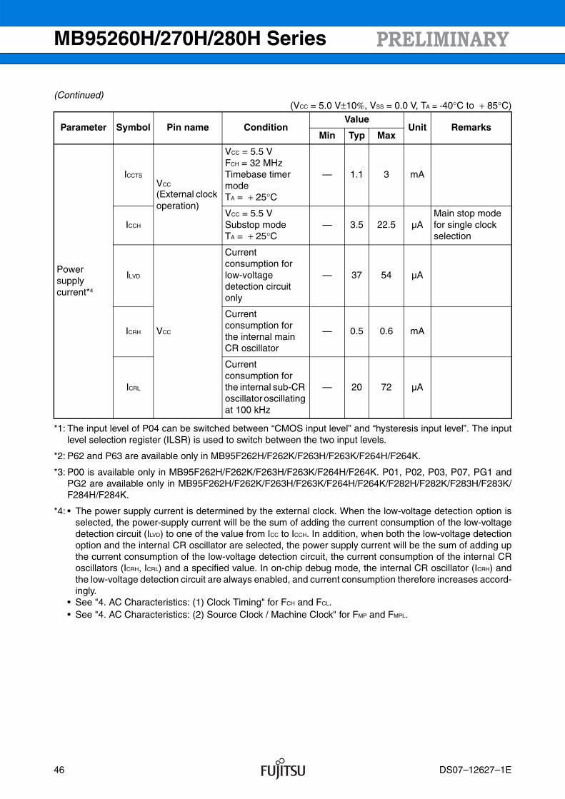
(Continued)(VCC = 5.0 V±10%, VSS = 0.0 V, TA = -40°C to + 85°C)
*1: The input level of P04 can be switched between “CMOS input level” and “hysteresis input level”. The inputlevel selection register (ILSR) is used to switch between the two input levels.
*2: P62 and P63 are available only in MB95F262H/F262K/F263H/F263K/F264H/F264K.
*3: P00 is available only in MB95F262H/F262K/F263H/F263K/F264H/F264K. P01, P02, P03, P07, PG1 andPG2 are available only in MB95F262H/F262K/F263H/F263K/F264H/F264K/F282H/F282K/F283H/F283K/F284H/F284K.
*4: • The power supply current is determined by the external clock. When the low-voltage detection option isselected, the power-supply current will be the sum of adding the current consumption of the low-voltagedetection circuit (ILVD) to one of the value from ICC to ICCH. In addition, when both the low-voltage detectionoption and the internal CR oscillator are selected, the power supply current will be the sum of adding upthe current consumption of the low-voltage detection circuit, the current consumption of the internal CRoscillators (ICRH, ICRL) and a specified value. In on-chip debug mode, the internal CR oscillator (ICRH) andthe low-voltage detection circuit are always enabled, and current consumption therefore increases accord-ingly.
• See "4. AC Characteristics: (1) Clock Timing" for FCH and FCL.• See "4. AC Characteristics: (2) Source Clock / Machine Clock" for FMP and FMPL.
Parameter Symbol Pin name ConditionValue
Unit RemarksMin Typ Max
Power supply current*4
ICCTS
VCC
(External clock operation)
VCC = 5.5 VFCH = 32 MHzTimebase timer modeTA = + 25°C
— 1.1 3 mA
ICCH
VCC = 5.5 VSubstop modeTA = + 25°C
— 3.5 22.5 µAMain stop mode for single clock selection
ILVD
VCC
Current consumption for low-voltage detection circuit only
— 37 54 µA
ICRH
Current consumption for the internal main CR oscillator
— 0.5 0.6 mA
ICRL
Current consumption for the internal sub-CR oscillator oscillating at 100 kHz
— 20 72 µA
46 DS07–12627–1E
MB95260H/270H/280H Series
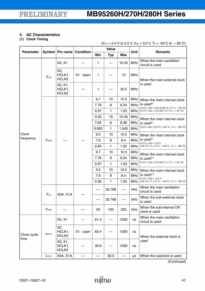
4. AC Characteristics(1) Clock Timing
(VCC = 2.4 V to 5.5 V, VSS = 0.0 V, TA = -40°C to + 85°C)
(Continued)
Parameter Symbol Pin name ConditionValue
Unit RemarksMin Typ Max
Clock frequency
FCH
X0, X1 — 1 — 16.25 MHzWhen the main oscillation circuit is used
X0, HCLK1, HCLK2
X1 : open 1 — 12 MHz
When the main external clock is usedX0, X1,
HCLK1, HCLK2
— 1 — 32.5 MHz
FCRH ⎯ —
9.7 10 10.3 MHz When the main internal clock is used*1
3.3 V ≤ Vcc ≤ 5.5 V(-40 °C ≤ TA ≤ + 40 °C)2.4 V ≤ Vcc < 3.3 V(0 °C ≤ TA ≤ + 40 °C)
7.76 8 8.24 MHz
0.97 1 1.03 MHz
9.55 10 10.45 MHzWhen the main internal clock is used*1
3.3 V ≤ Vcc ≤ 5.5 V ( + 40 °C < TA ≤ + 85 °C)
7.64 8 8.36 MHz
0.955 1 1.045 MHz
9.5 10 10.5 MHz When the main internal clock is used*1
2.4 V ≤ Vcc < 3.3 V(-40 °C ≤ TA < 0 °C, + 40 °C < TA ≤ + 85 °C)
7.6 8 8.4 MHz
0.95 1 1.05 MHz
9.7 10 10.3 MHzWhen the main internal clock is used*2
2.4 V ≤ Vcc ≤ 5.5 V(0 °C ≤ TA ≤ + 40 °C)
7.76 8 8.24 MHz
0.97 1 1.03 MHz
9.5 10 10.5 MHz When the main internal clock is used*2
2.4 V ≤ Vcc ≤ 5.5 V(-40 °C ≤ TA < 0 °C, + 40 °C < TA ≤ + 85 °C)
7.6 8 8.4 MHz
0.95 1 1.05 MHz
FCL X0A, X1A —
— 32.768 — kHzWhen the main oscillation circuit is used
— 32.768 — kHzWhen the sub-external clock is used
FCRL ⎯ — 50 100 200 kHzWhen the sub-internal CR clock is used
Clock cycle time
tHCYL
X0, X1 — 61.5 — 1000 nsWhen the main oscillation circuit is used
X0, HCLK1, HCLK2
X1 : open 83.4 — 1000 ns
When the external clock is usedX0, X1,
HCLK1, HCLK2
— 30.8 — 1000 ns
tLCYL X0A, X1A — — 30.5 — µs When the subclock is used
DS07–12627–1E 47
MB95260H/270H/280H Series
(Continued)(VCC = 2.4 V to 5.5 V, VSS = 0.0 V, TA = -40°C to + 85°C)
*1: These specifications are not applicable to the following products: MB95F272HPH, MB95F272KPH, MB95F273HPH, MB95F273KPH, MB95F274HPH and MB95F274KPH.
*2: These specifcations are only applicable to the following products: MB95F272HPH, MB95F272KPH, MB95F273HPH, MB95F273KPH, MB95F274HPH and MB95F274KPH.
Parameter Symbol Pin name ConditionValue
Unit RemarksMin Typ Max
Input clock pulse width
tWH1
tWL1
X0, HCLK1, HCLK2
X1 : open 33.4 — — ns
When the external clock is used, the duty ratio should range between 40% and 60%.
X0, X1, HCLK1, HCLK2
— 12.4 — — ns
tWH2
tWL2X0A — — 15.2 — µs
Input clock rise time and fall time
tCR
tCF
X0, HCLK1, HCLK2
X1 : open — — 5 ns
When the external clock is usedX0, X1
HCLK1, HCLK2
— — — 5 ns
Internal CR oscillation start time
tCRHWK — — — — 80 µsWhen the main internal CR clock is used
tCRLWK — — — — 10 µsWhen the sub-internal CR clock is used
48 DS07–12627–1E
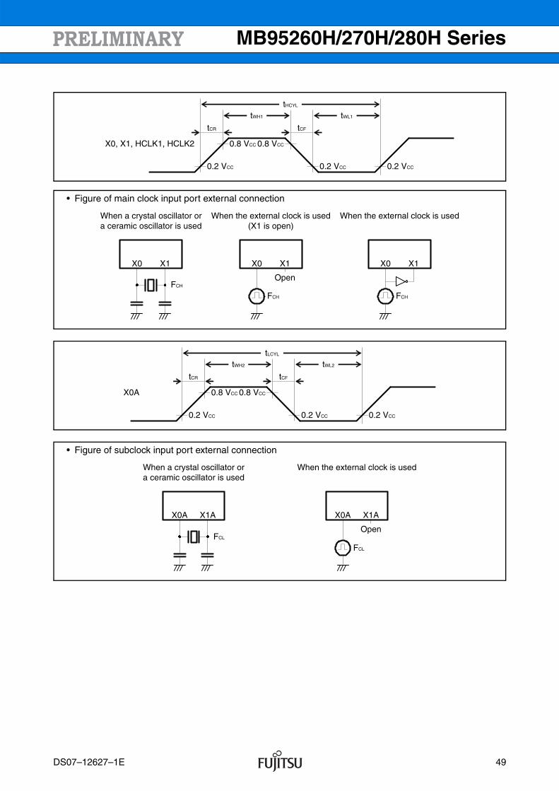
MB95260H/270H/280H Series
X0, X1, HCLK1, HCLK2 0.8 VCC
0.2 VCC 0.2 VCC
0.8 VCC
tWH1 tWL1
0.2 VCC
tHCYL
tCR tCF
When a crystal oscillator ora ceramic oscillator is used
When the external clock is used
X0 X1 X0 X1
FCH
FCH
When the external clock is used(X1 is open)
X0 X1
Open
FCH
• Figure of main clock input port external connection
X0A 0.8 VCC
0.2 VCC 0.2 VCC
0.8 VCC
tWH2 tWL2
0.2 VCC
tLCYL
tCR tCF
When a crystal oscillator ora ceramic oscillator is used
When the external clock is used
X0A X1A X0A X1A
OpenFCL
FCL
• Figure of subclock input port external connection
DS07–12627–1E 49
MB95260H/270H/280H Series
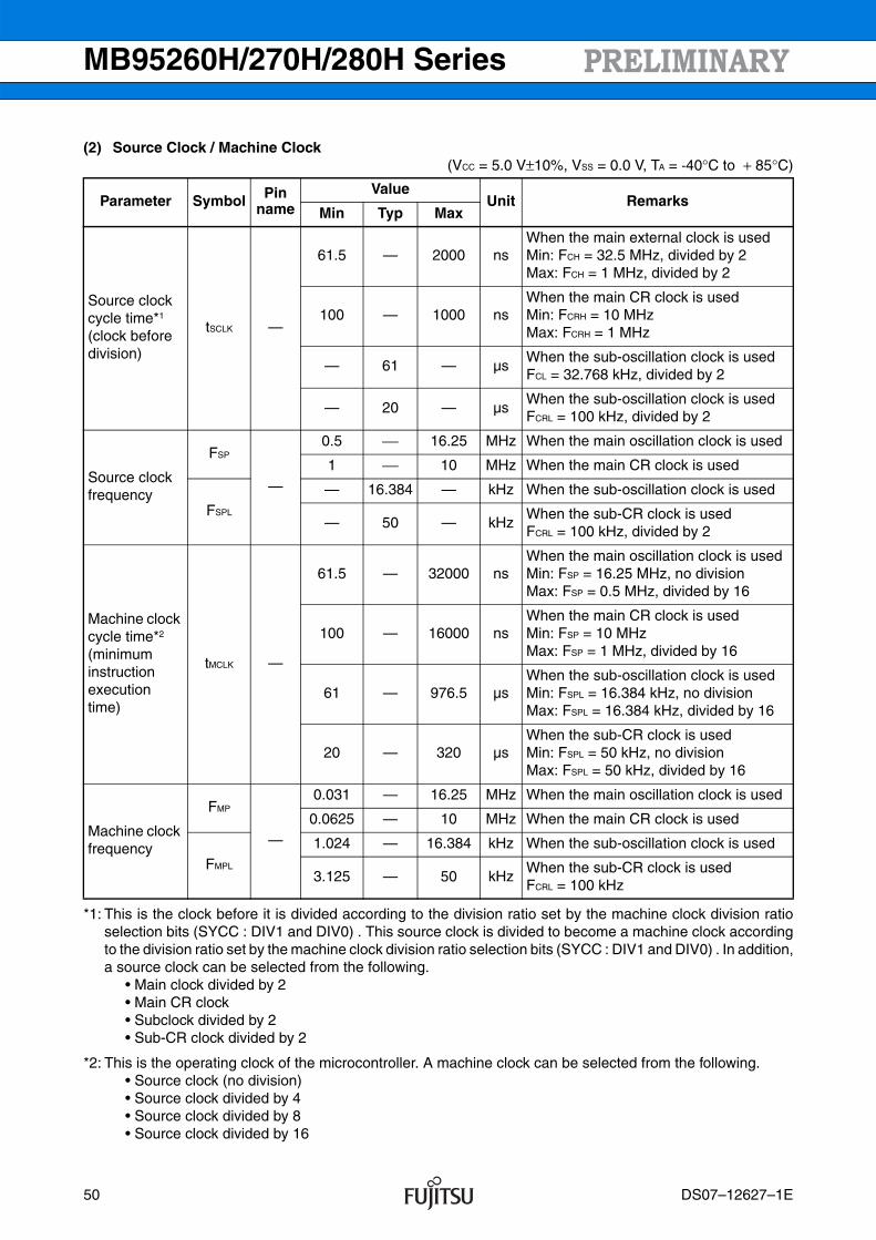
(2) Source Clock / Machine Clock (VCC = 5.0 V±10%, VSS = 0.0 V, TA = -40°C to + 85°C)
*1: This is the clock before it is divided according to the division ratio set by the machine clock division ratioselection bits (SYCC : DIV1 and DIV0) . This source clock is divided to become a machine clock accordingto the division ratio set by the machine clock division ratio selection bits (SYCC : DIV1 and DIV0) . In addition,a source clock can be selected from the following.
• Main clock divided by 2• Main CR clock• Subclock divided by 2• Sub-CR clock divided by 2
*2: This is the operating clock of the microcontroller. A machine clock can be selected from the following.• Source clock (no division)• Source clock divided by 4• Source clock divided by 8• Source clock divided by 16
Parameter Symbol Pin name
ValueUnit Remarks
Min Typ Max
Source clock cycle time*1
(clock before division)
tSCLK —
61.5 — 2000 nsWhen the main external clock is usedMin: FCH = 32.5 MHz, divided by 2Max: FCH = 1 MHz, divided by 2
100 — 1000 nsWhen the main CR clock is usedMin: FCRH = 10 MHzMax: FCRH = 1 MHz
— 61 — µsWhen the sub-oscillation clock is usedFCL = 32.768 kHz, divided by 2
— 20 — µsWhen the sub-oscillation clock is usedFCRL = 100 kHz, divided by 2
Source clock frequency
FSP
—
0.5 ⎯ 16.25 MHz When the main oscillation clock is used
1 ⎯ 10 MHz When the main CR clock is used
FSPL
— 16.384 — kHz When the sub-oscillation clock is used
— 50 — kHzWhen the sub-CR clock is usedFCRL = 100 kHz, divided by 2
Machine clock cycle time*2
(minimum instruction execution time)
tMCLK —
61.5 — 32000 nsWhen the main oscillation clock is usedMin: FSP = 16.25 MHz, no divisionMax: FSP = 0.5 MHz, divided by 16
100 — 16000 nsWhen the main CR clock is usedMin: FSP = 10 MHzMax: FSP = 1 MHz, divided by 16
61 — 976.5 µsWhen the sub-oscillation clock is usedMin: FSPL = 16.384 kHz, no divisionMax: FSPL = 16.384 kHz, divided by 16
20 — 320 µsWhen the sub-CR clock is usedMin: FSPL = 50 kHz, no divisionMax: FSPL = 50 kHz, divided by 16
Machine clock frequency
FMP
—
0.031 — 16.25 MHz When the main oscillation clock is used
0.0625 — 10 MHz When the main CR clock is used
FMPL
1.024 — 16.384 kHz When the sub-oscillation clock is used
3.125 — 50 kHzWhen the sub-CR clock is usedFCRL = 100 kHz
50 DS07–12627–1E
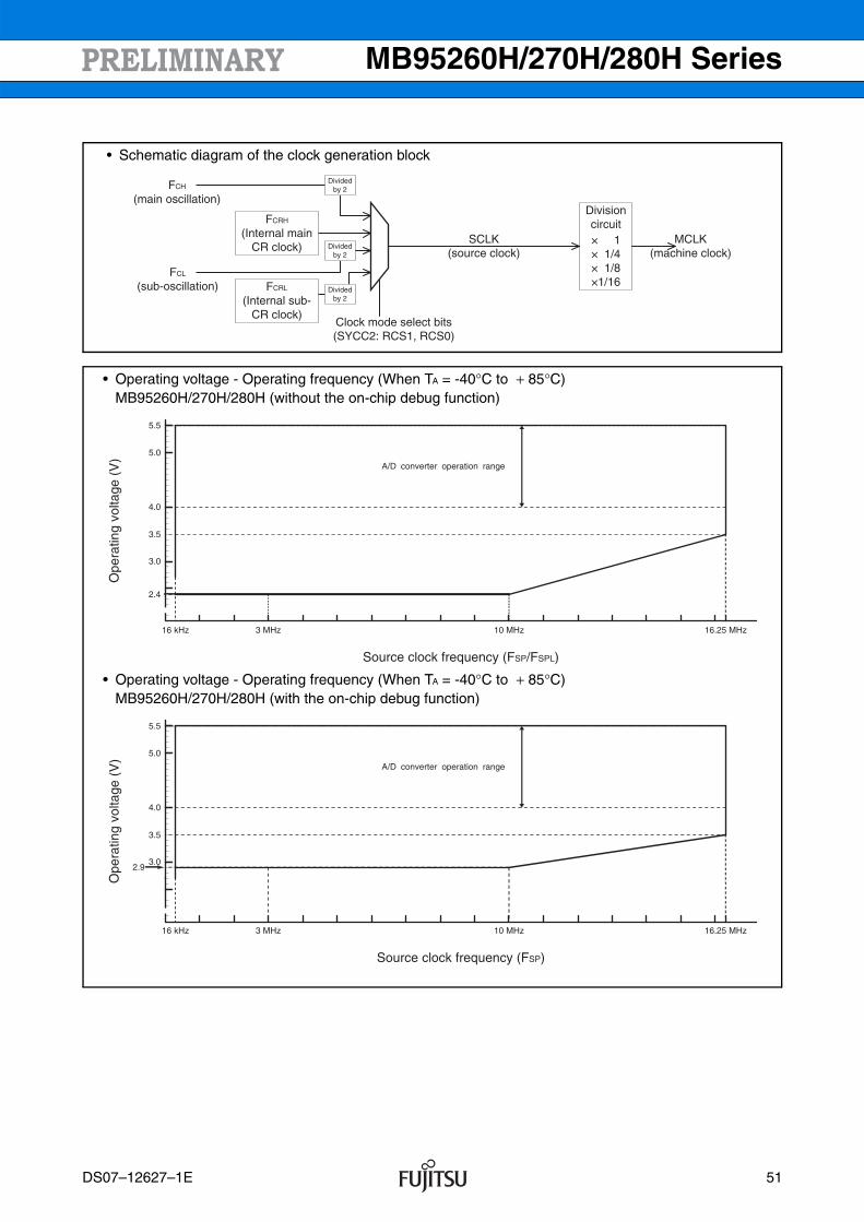
MB95260H/270H/280H Series
FCH
(main oscillation)
FCRH
(Internal mainCR clock)
FCL
(sub-oscillation) FCRL
(Internal sub-CR clock)
SCLK(source clock)
MCLK(machine clock)
Clock mode select bits(SYCC2: RCS1, RCS0)
Divisioncircuit××××
11/41/8
1/16Divided
by 2
Dividedby 2
Dividedby 2
• Schematic diagram of the clock generation block
Ope
ratin
g vo
ltage
(V
)
A/D converter operation range
5.5
5.0
4.0
3.5
3.0
2.4
16 kHz 3 MHz 10 MHz 16.25 MHz
Source clock frequency (FSP/FSPL)
Ope
ratin
g vo
ltage
(V
)
A/D converter operation range
5.5
5.0
4.0
3.5
3.02.9
16 kHz 3 MHz 10 MHz 16.25 MHz
Source clock frequency (FSP)
• Operating voltage - Operating frequency (When TA = -40°C to + 85°C)MB95260H/270H/280H (without the on-chip debug function)
• Operating voltage - Operating frequency (When TA = -40°C to + 85°C)MB95260H/270H/280H (with the on-chip debug function)
DS07–12627–1E 51
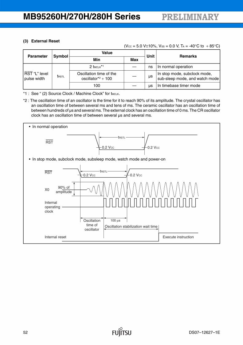
MB95260H/270H/280H Series
(3) External Reset (VCC = 5.0 V±10%, VSS = 0.0 V, TA = -40°C to + 85°C)
*1 : See “ (2) Source Clock / Machine Clock” for tMCLK.
*2 : The oscillation time of an oscillator is the time for it to reach 90% of its amplitude. The crystal oscillator hasan oscillation time of between several ms and tens of ms. The ceramic oscillator has an oscillation time ofbetween hundreds of µs and several ms. The external clock has an oscillation time of 0 ms. The CR oscillatorclock has an oscillation time of between several µs and several ms.
Parameter SymbolValue
Unit RemarksMin Max
RST “L” level pulse width
tRSTL
2 tMCLK*1 — ns In normal operation
Oscillation time of the oscillator*2 + 100
— µsIn stop mode, subclock mode, sub-sleep mode, and watch mode
100 — µs In timebase timer mode
0.2 VCC
RST0.2 VCC
tRSTL
tRSTL
0.2 VCC 0.2 VCC
100 µs
X0
Internaloperatingclock
90% ofamplitude
Oscillationtime of
oscillatorOscillation stabilization wait time
Execute instructionInternal reset
RST
• In normal operation
• In stop mode, subclock mode, subsleep mode, watch mode and power-on
52 DS07–12627–1E
MB95260H/270H/280H Series
(4) Power-on Reset (VSS = 0.0 V, TA = -40°C to + 85°C)
Note: A sudden change of power supply voltage may activate the power-on reset function. When changing thepower supply voltage during the operation, set the slope of rising to a value below within 30 mV/ms asshown below.
Parameter Symbol ConditionValue
Unit RemarksMin Max
Power supply rising time tR — — 50 ms
Power supply cutoff time tOFF — 1 — ms Wait time until power-on
0.2 V0.2 V
tOFFtR
2.5 V
0.2 VVCC
VCC
2.3 V
VSS
Hold condition in stop mode
Set the slope of rising toa value below 30 mV/ms.
DS07–12627–1E 53
MB95260H/270H/280H Series
(5) Peripheral Input Timing (VCC = 5.0 V±10%, VSS = 0.0 V, TA = -40°C to + 85°C)
*1: See “(2) Source Clock / Machine Clock” for tMCLK.
*2: INT04, INT06 and EC0 are available in all products.
*3: INT02, INT03, INT05 and INT07 are available only in MB95F262H/F262K/F263H/F263K/F264H/F264K/F282H/F282K/F283H/F283K/F284H/F284K.
*4: EC1 is available only in MB95F262H/F262K/F263H/F263K/F264H/F264K.
Parameter Symbol Pin nameValue
UnitMin Max
Peripheral input “H” pulse width tILIHINT02 to INT07*2,*3, EC0*2, EC1*4
2 tMCLK*1 — ns
Peripheral input “L” pulse width tIHIL 2 tMCLK*1 — ns
INT02 to INT07*2, *3,EC0*2, EC1*4
0.8 VCC 0.8 VCC
0.2 VCC 0.2 VCC
tILIH tIHIL
54 DS07–12627–1E
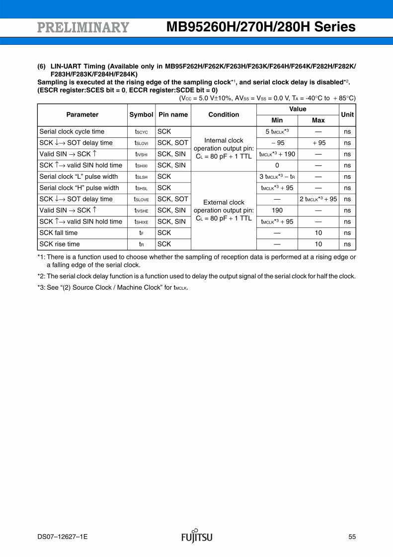
MB95260H/270H/280H Series
(6) LIN-UART Timing (Available only in MB95F262H/F262K/F263H/F263K/F264H/F264K/F282H/F282K/F283H/F283K/F284H/F284K)
Sampling is executed at the rising edge of the sampling clock*1, and serial clock delay is disabled*2.(ESCR register:SCES bit = 0, ECCR register:SCDE bit = 0)
(VCC = 5.0 V±10%, AVSS = VSS = 0.0 V, TA = -40°C to + 85°C)
*1: There is a function used to choose whether the sampling of reception data is performed at a rising edge ora falling edge of the serial clock.
*2: The serial clock delay function is a function used to delay the output signal of the serial clock for half the clock.
*3: See “(2) Source Clock / Machine Clock” for tMCLK.
Parameter Symbol Pin name ConditionValue
UnitMin Max
Serial clock cycle time tSCYC SCKInternal clock
operation output pin:CL = 80 pF + 1 TTL
5 tMCLK*3 — ns
SCK ↓→ SOT delay time tSLOVI SCK, SOT − 95 + 95 ns
Valid SIN → SCK ↑ tIVSHI SCK, SIN tMCLK*3 + 190 — ns
SCK ↑→ valid SIN hold time tSHIXI SCK, SIN 0 — ns
Serial clock “L” pulse width tSLSH SCK
External clockoperation output pin:CL = 80 pF + 1 TTL
3 tMCLK*3 − tR — ns
Serial clock “H” pulse width tSHSL SCK tMCLK*3 + 95 — ns
SCK ↓→ SOT delay time tSLOVE SCK, SOT — 2 tMCLK*3 + 95 ns
Valid SIN → SCK ↑ tIVSHE SCK, SIN 190 — ns
SCK ↑→ valid SIN hold time tSHIXE SCK, SIN tMCLK*3 + 95 — ns
SCK fall time tF SCK — 10 ns
SCK rise time tR SCK — 10 ns
DS07–12627–1E 55
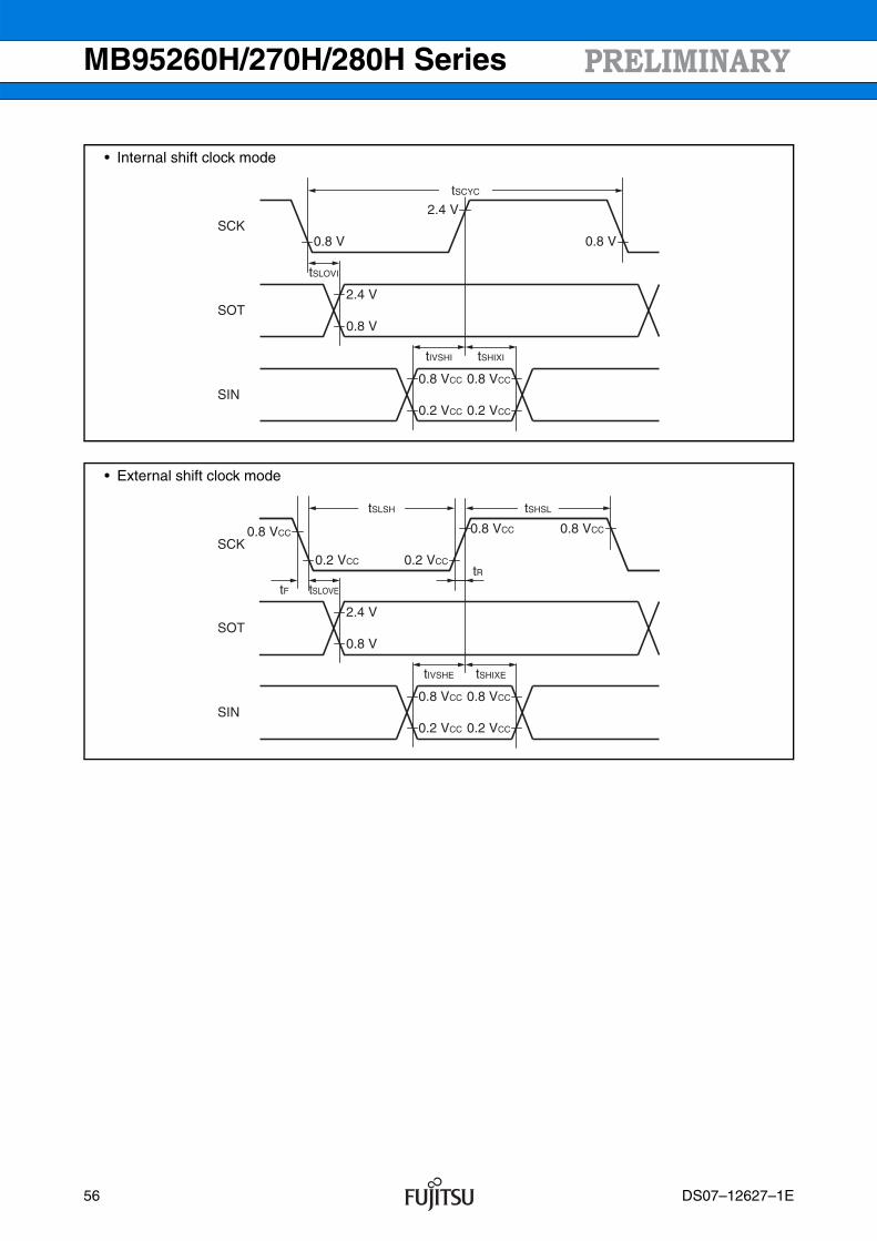
MB95260H/270H/280H Series
0.8 V 0.8 V
2.4 V
tSLOVI
tIVSHI tSHIXI
2.4 V
0.8 V
SCK
SOT
SIN0.8 VCC
0.2 VCC
0.8 VCC
0.2 VCC
tSCYC
• Internal shift clock mode
0.2 VCC 0.2 VCC
0.8 VCC 0.8 VCC
tSLOVE
tIVSHE tSHIXE
2.4 V
0.8 V
SCK
SOT
SIN0.8 VCC
0.2 VCC
0.8 VCC
0.2 VCC
tSLSH tSHSL
tR
0.8 VCC
tF
• External shift clock mode
56 DS07–12627–1E
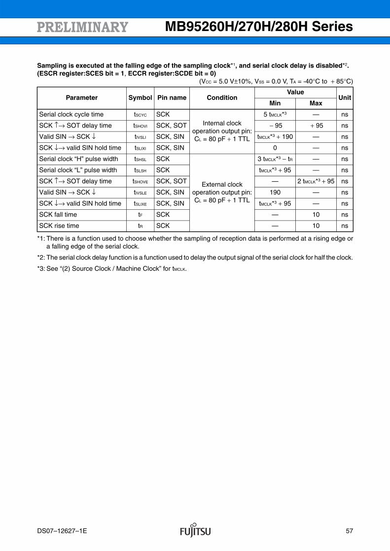
MB95260H/270H/280H Series
Sampling is executed at the falling edge of the sampling clock*1, and serial clock delay is disabled*2.(ESCR register:SCES bit = 1, ECCR register:SCDE bit = 0)
(VCC = 5.0 V±10%, VSS = 0.0 V, TA = -40°C to + 85°C)
*1: There is a function used to choose whether the sampling of reception data is performed at a rising edge ora falling edge of the serial clock.
*2: The serial clock delay function is a function used to delay the output signal of the serial clock for half the clock.
*3: See “(2) Source Clock / Machine Clock” for tMCLK.
Parameter Symbol Pin name ConditionValue
UnitMin Max
Serial clock cycle time tSCYC SCKInternal clock
operation output pin:CL = 80 pF + 1 TTL
5 tMCLK*3 — ns
SCK ↑→ SOT delay time tSHOVI SCK, SOT − 95 + 95 ns
Valid SIN → SCK ↓ tIVSLI SCK, SIN tMCLK*3 + 190 — ns
SCK ↓→ valid SIN hold time tSLIXI SCK, SIN 0 — ns
Serial clock “H” pulse width tSHSL SCK
External clockoperation output pin:CL = 80 pF + 1 TTL
3 tMCLK*3 − tR — ns
Serial clock “L” pulse width tSLSH SCK tMCLK*3 + 95 — ns
SCK ↑→ SOT delay time tSHOVE SCK, SOT — 2 tMCLK*3 + 95 ns
Valid SIN → SCK ↓ tIVSLE SCK, SIN 190 — ns
SCK ↓→ valid SIN hold time tSLIXE SCK, SIN tMCLK*3 + 95 — ns
SCK fall time tF SCK — 10 ns
SCK rise time tR SCK — 10 ns
DS07–12627–1E 57
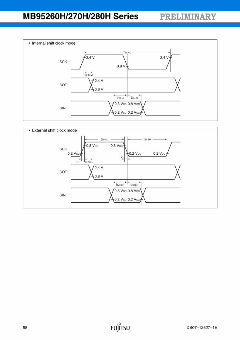
MB95260H/270H/280H Series
0.8 V
2.4 V2.4 V
tSHOVI
tIVSLI tSLIXI
2.4 V
0.8 V
SCK
SOT
SIN0.8 VCC
0.2 VCC
0.8 VCC
0.2 VCC
tSCYC
• Internal shift clock mode
0.2 VCC 0.2 VCC 0.2 VCC
0.8 VCC
tSHOVE
tIVSLE tSLIXE
2.4 V
0.8 V
SCK
SOT
SIN0.8 VCC
0.2 VCC
0.8 VCC
0.2 VCC
tSHSL tSLSH
tF
0.8 VCC
tR
• External shift clock mode
58 DS07–12627–1E
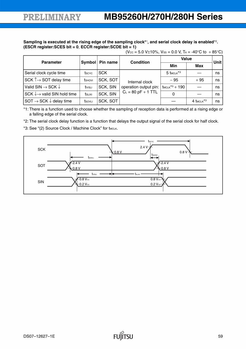
MB95260H/270H/280H Series
Sampling is executed at the rising edge of the sampling clock*1, and serial clock delay is enabled*2.(ESCR register:SCES bit = 0, ECCR register:SCDE bit = 1)
(VCC = 5.0 V±10%, VSS = 0.0 V, TA = -40°C to + 85°C)
*1: There is a function used to choose whether the sampling of reception data is performed at a rising edge ora falling edge of the serial clock.
*2: The serial clock delay function is a function that delays the output signal of the serial clock for half clock.
*3: See “(2) Source Clock / Machine Clock” for tMCLK.
Parameter Symbol Pin name ConditionValue
UnitMin Max
Serial clock cycle time tSCYC SCK
Internal clockoperation output pin:CL = 80 pF + 1 TTL
5 tMCLK*3 — ns
SCK ↑→ SOT delay time tSHOVI SCK, SOT − 95 + 95 ns
Valid SIN → SCK ↓ tIVSLI SCK, SIN tMCLK*3 + 190 — ns
SCK ↓→ valid SIN hold time tSLIXI SCK, SIN 0 — ns
SOT → SCK ↓ delay time tSOVLI SCK, SOT — 4 tMCLK*3 ns
2.4 V
0.8 V 0.8 VtSHOVI
tSOVLI
tIVSLI tSLIXI
2.4 V
0.8 V
2.4 V
0.8 V
SCK
SOT
SIN0.8 VCC
0.2 VCC
0.8 VCC
0.2 VCC
tSCYC
DS07–12627–1E 59
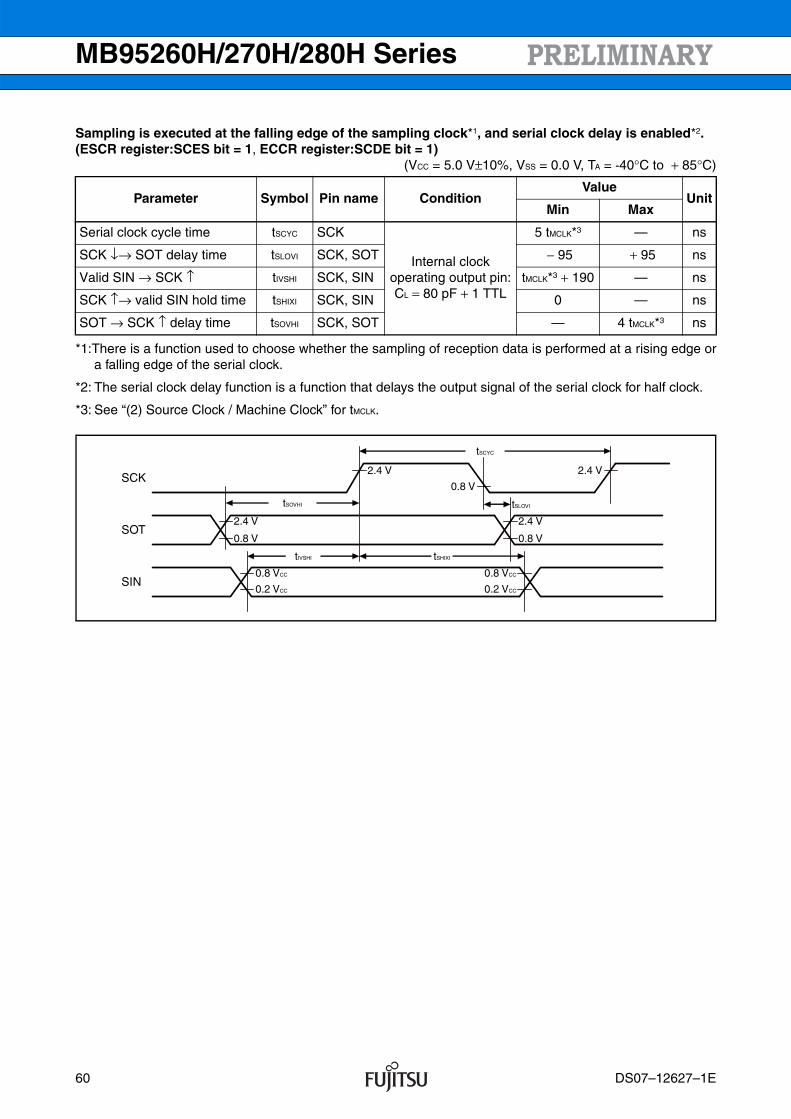
MB95260H/270H/280H Series
Sampling is executed at the falling edge of the sampling clock*1, and serial clock delay is enabled*2.(ESCR register:SCES bit = 1, ECCR register:SCDE bit = 1)
(VCC = 5.0 V±10%, VSS = 0.0 V, TA = -40°C to + 85°C)
*1:There is a function used to choose whether the sampling of reception data is performed at a rising edge ora falling edge of the serial clock.
*2: The serial clock delay function is a function that delays the output signal of the serial clock for half clock.
*3: See “(2) Source Clock / Machine Clock” for tMCLK.
Parameter Symbol Pin name ConditionValue
UnitMin Max
Serial clock cycle time tSCYC SCK
Internal clock operating output pin:CL = 80 pF + 1 TTL
5 tMCLK*3 — ns
SCK ↓→ SOT delay time tSLOVI SCK, SOT − 95 + 95 ns
Valid SIN → SCK ↑ tIVSHI SCK, SIN tMCLK*3 + 190 — ns
SCK ↑→ valid SIN hold time tSHIXI SCK, SIN 0 — ns
SOT → SCK ↑ delay time tSOVHI SCK, SOT — 4 tMCLK*3 ns
0.8 V
2.4 V 2.4 V
tSLOVItSOVHI
tIVSHI tSHIXI
2.4 V
0.8 V
2.4 V
0.8 V
SCK
SOT
SIN0.8 VCC
0.2 VCC
0.8 VCC
0.2 VCC
tSCYC
60 DS07–12627–1E
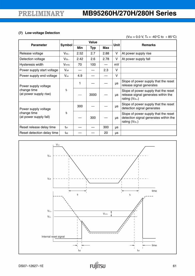
MB95260H/270H/280H Series
(7) Low-voltage Detection(VSS = 0.0 V, TA = -40°C to + 85°C)
Parameter SymbolValue
Unit RemarksMin Typ Max
Release voltage VDL+ 2.52 2.7 2.88 V At power supply rise
Detection voltage VDL− 2.42 2.6 2.78 V At power supply fall
Hysteresis width VHYS 70 100 — mV
Power supply start voltage Voff — — 2.3 V
Power supply end voltage Von 4.9 — — V
Power supply voltage change time(at power supply rise)
tr
1 — — µsSlope of power supply that the reset release signal generates
⎯ 3000 — µsSlope of power supply that the reset release signal generates within the rating (VDL+)
Power supply voltage change time(at power supply fall)
tf
300 — — µsSlope of power supply that the reset detection signal generates
— 300 — µsSlope of power supply that the reset detection signal generates within the rating (VDL-)
Reset release delay time td1 — — 300 µs
Reset detection delay time td2 — — 20 µs
VHYS
td2 td1
trtf
VCC
Internal reset signal
Von
Voff
VDL+
VDL-
time
time
DS07–12627–1E 61
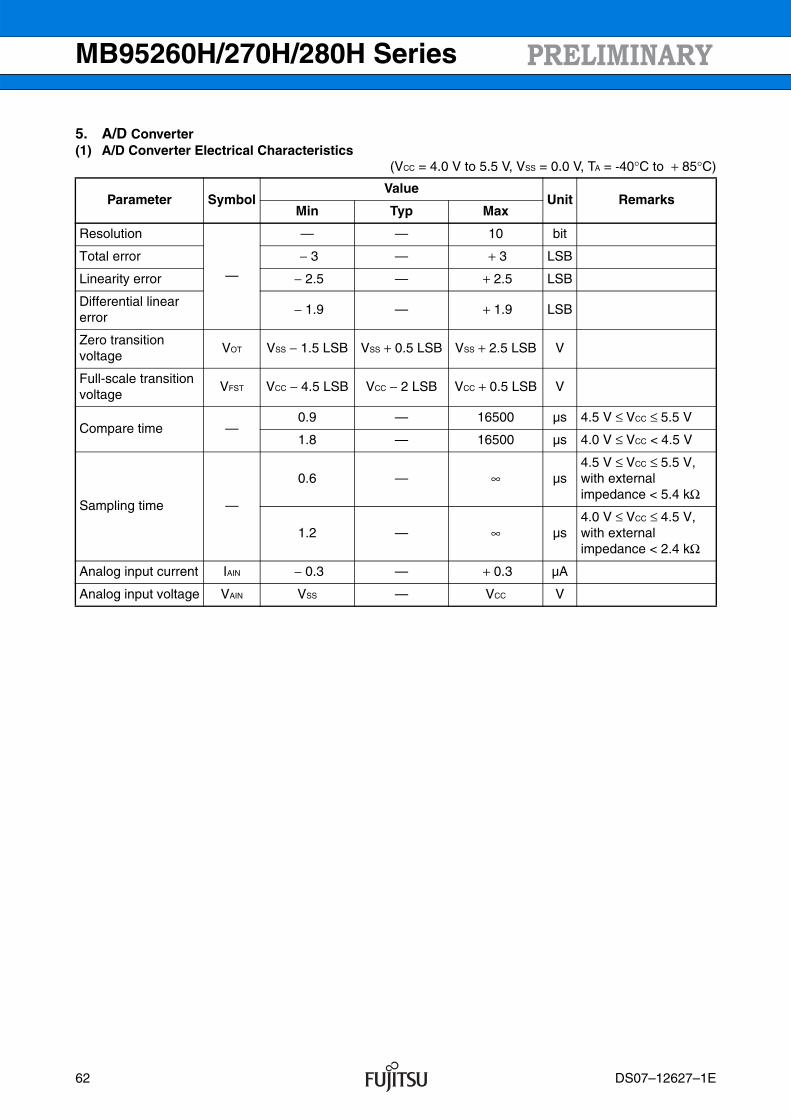
MB95260H/270H/280H Series
5. A/D Converter(1) A/D Converter Electrical Characteristics
(VCC = 4.0 V to 5.5 V, VSS = 0.0 V, TA = -40°C to + 85°C)
Parameter SymbolValue
Unit RemarksMin Typ Max
Resolution
—
— — 10 bit
Total error − 3 — + 3 LSB
Linearity error − 2.5 — + 2.5 LSB
Differential linearerror
− 1.9 — + 1.9 LSB
Zero transitionvoltage
VOT VSS − 1.5 LSB VSS + 0.5 LSB VSS + 2.5 LSB V
Full-scale transition voltage
VFST VCC − 4.5 LSB VCC − 2 LSB VCC + 0.5 LSB V
Compare time —0.9 — 16500 µs 4.5 V ≤ VCC ≤ 5.5 V
1.8 — 16500 µs 4.0 V ≤ VCC < 4.5 V
Sampling time —
0.6 — ∞ µs4.5 V ≤ VCC ≤ 5.5 V, with external impedance < 5.4 kΩ
1.2 — ∞ µs4.0 V ≤ VCC ≤ 4.5 V, with external impedance < 2.4 kΩ
Analog input current IAIN − 0.3 — + 0.3 µA
Analog input voltage VAIN VSS — VCC V
62 DS07–12627–1E
MB95260H/270H/280H Series
(2) Notes on Using the A/D Converter• External impedance of analog input and its sampling time
• The A/D converter has a sample and hold circuit. If the external impedance is too high to keep sufficientsampling time, the analog voltage charged to the capacitor of the internal sample and hold circuit isinsufficient, adversely affecting A/D conversion precision. Therefore, to satisfy the A/D conversion precisionstandard, considering the relationship between the external impedance and minimum sampling time, eitheradjust the register value and operating frequency or decrease the external impedance so that the samplingtime is longer than the minimum value. In addition, if sufficient sampling time cannot be secured, connecta capacitor of about 0.1 µF to the analog input pin.
• A/D conversion error
As |VCC−VSS| decreases, the A/D conversion error increases proportionately.
ComparatorAnalog input
During sampling: ON
Note: The values are reference values.
~~ ~~4.5 V < VCC < 5.5 V : R 1.95 kΩ (Max), C 17 pF (Max)~~ ~~<4.0 V VCC < 4.5 V : R 8.98 kΩ (Max), C 17 pF (Max)
R C
• Analog input equivalent circuit
[External impedance = 0 kΩ to 100 kΩ]
Ext
erna
l im
peda
nce
[kΩ
]
Ext
erna
l im
peda
nce
[kΩ
]
Minimum sampling time [µs] Minimum sampling time [µs]
[External impedance = 0 kΩ to 20 kΩ]
100
90
80
70
60
50
40
30
20
10
0
20
18
16
14
12
10
8
6
4
2
0
0 2 4 6 8 10 12 14 10 2 3 4
(VCC > 4.5 V)
(VCC > 4.0 V)
(VCC > 4.5 V)
(VCC > 4.0 V)
• Relationship between external impedance and minimum sampling time
DS07–12627–1E 63
MB95260H/270H/280H Series
(3) Definitions of A/D Converter Terms• Resolution
It indicates the level of analog variation that can be distinguished by the A/D converter.When the number of bits is 10, analog voltage can be divided into 210 = 1024.
• Linearity error (unit: LSB)It indicates how much an actual conversion value deviates from the straight line connectingthe zero transition point (“00 0000 0000” ← → “00 0000 0001”) of a device tothe full-scale transition point (“11 1111 1111” ← → “11 1111 1110”) of the same device.
• Differential linear error (unit: LSB)It indicates how much the input voltage required to change the output code by 1 LSB deviates from anideal value.
• Total error (unit: LSB)It indicates the difference between an actual value and a theoretical value. The error can be caused by azero transition error, a full-scale transition errors, a linearity error, a quantum error, or noise.
(Continued)
VSS
VFST
Ideal I/O characteristics
VCC
001H
002H
003H
004H
3FDH
3FEH
3FFH
Dig
ital o
utpu
t
Dig
ital o
utpu
t
2 LSB
VOT
1 LSB
0.5 LSB
Total error
Analog inputAnalog input
001H
002H
003H
004H
3FDH
3FEH
3FFH
Actual conversioncharacteristic
Ideal characteristic
Actual conversioncharacteristic
N
VNT
: A/D converter digital output value
: Voltage at which the digital output transits from (N - 1)H to NH
1 LSB x (N-1) + 0.5 LSB
VNT
VSS VCC
Total error ofdigital output N
VNT - 1 LSB × (N - 1) + 0.5 LSB1 LSB
[LSB]=VCC - VSS
1024(V)1 LSB =
64 DS07–12627–1E
MB95260H/270H/280H Series
(Continued)
Zero transition error
Linearity error
Full-scale transition error
001H
002H
003H
004H
3FDH
3FEH
3FFH
Dig
ital o
utpu
t
Differential linear errorof digital output N
V(N+1)T - VNT
1 LSB- 1=
Linearity errorof digital output N
VNT - 1 LSB × N + VOT1 LSB
=
Dig
ital o
utpu
t
Analog input
001H
002H
3FCH
3FDH
003H
3FEH
3FFH
004H
Actual conversioncharacteristic
Actual conversioncharacteristic
VOT (measurement value)
Actual conversioncharacteristic
Actual conversioncharacteristic
VFST
(measurementvalue)
VSS VCC
Analog inputVSS VCC
Dig
ital o
utpu
t
Analog inputVSS VCC
Ideal characteristic
1 LSB × N + VOT
Actual conversioncharacteristic
Idealcharacteristic
Actual conversioncharacteristic
VOT (measurement value)
VNT
Differential linearity error
(N - 2)H
(N - 1)H
NH
(N + 1)H
Dig
ital o
utpu
t
Analog inputVSS VCC
Actual conversioncharacteristic
Ideal characteristic
VNT
Actual conversioncharacteristic
V(N+1)T
N
VNT
: A/D converter digital output value
: Voltage at which the digital output transits from (N - 1)H to NH
VOT (ideal value) = VSS + 0.5 LSB [V]
VFST (ideal value) = VCC - 2 LSB [V]
VFST
(measurementvalue)
Idealcharacteristic
DS07–12627–1E 65
MB95260H/270H/280H Series
6. Flash Memory Write/Erase Characteristics
*1: TA = + 25°C, VCC = 5.0 V, 100000 cycles
*2: TA = + 110°C, VCC = 4.5 V, 10000 cycles
*3: The typical value of the number of erase/write cycles is 100000 provided that TA is lower than + 85°C. WhenTA is higher than + 85°C, the typical value becomes 10000 cycles only.
*4: This value is converted from the result of a technology reliability assessment. (The value is converted fromthe result of a high temperature accelerated test using the Arrhenius equation with the average temperaturebeing + 85°C) .
ParameterValue
Unit RemarksMin Typ Max
Sector erase time(16 Kbytes sector)
— 0.5*1 7.5*2 sThe time of writing 00H prior to erasure is excluded.
Sector erase time(2 Kbytes sector)
— 0.2*1 0.5*2 sThe time of writing 00H prior to erasure is excluded.
Byte writing time — 21 6100*2 µs System-level overhead is excluded.
Erase / write cycle — 100000*3 — cycle
Power supply voltage at erase/write
4.5 — 5.5 V
Flash memory data retention time
20*4 — — year Average TA = + 85°C
66 DS07–12627–1E
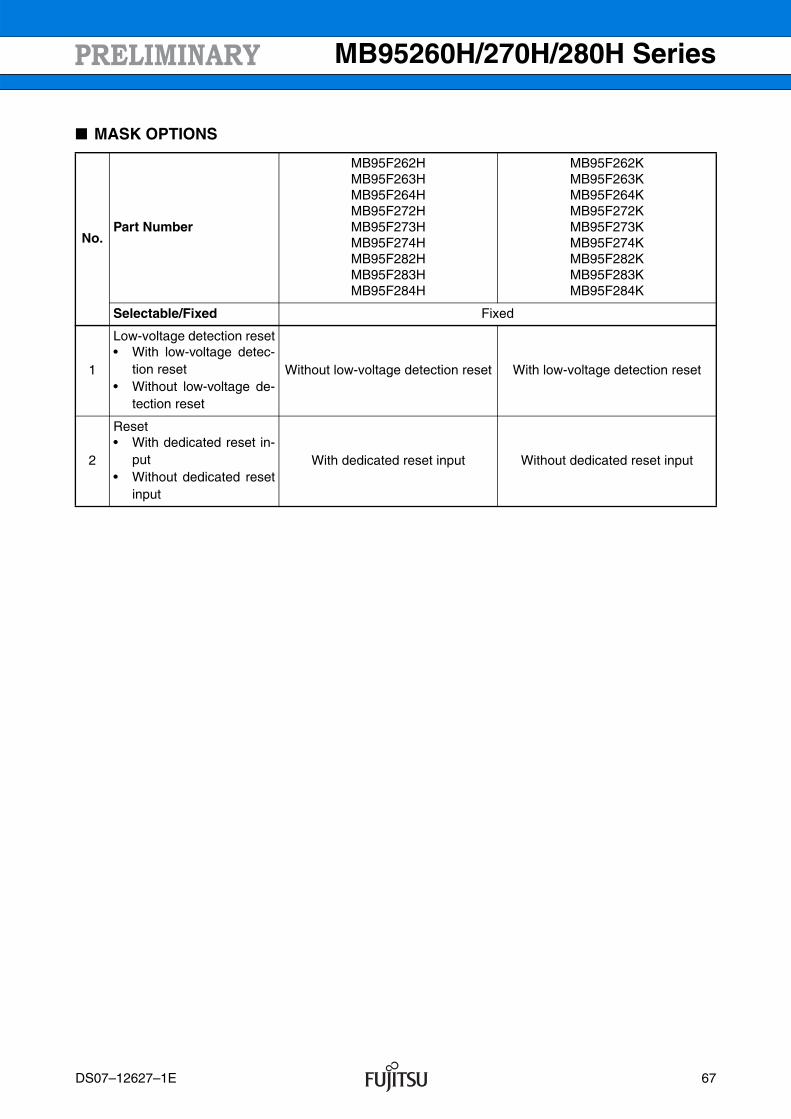
MB95260H/270H/280H Series
MASK OPTIONS
No.Part Number
MB95F262HMB95F263HMB95F264HMB95F272HMB95F273HMB95F274HMB95F282HMB95F283HMB95F284H
MB95F262KMB95F263KMB95F264KMB95F272KMB95F273KMB95F274KMB95F282KMB95F283KMB95F284K
Selectable/Fixed Fixed
1
Low-voltage detection reset• With low-voltage detec-
tion reset• Without low-voltage de-
tection reset
Without low-voltage detection reset With low-voltage detection reset
2
Reset• With dedicated reset in-
put• Without dedicated reset
input
With dedicated reset input Without dedicated reset input
DS07–12627–1E 67
MB95260H/270H/280H Series
ORDERING INFORMATION
Part Number Package
MB95F262HP-G-SH-SNE2MB95F262KP-G-SH-SNE2MB95F263HP-G-SH-SNE2MB95F263KP-G-SH-SNE2MB95F264HP-G-SH-SNE2MB95F264KP-G-SH-SNE2
24-pin plastic DIP(DIP-24P-M07)
MB95F262HPF-G-SNE2MB95F262KPF-G-SNE2MB95F263HPF-G-SNE2MB95F263KPF-G-SNE2MB95F264HPF-G-SNE2MB95F264KPF-G-SNE2
20-pin plastic SOP(FPT-20P-M09)
MB95F262HPFT-G-SNE2MB95F262KPFT-G-SNE2MB95F263HPFT-G-SNE2MB95F263KPFT-G-SNE2MB95F264HPFT-G-SNE2MB95F264KPFT-G-SNE2
20-pin plastic TSSOP(FPT-20P-M10)*Under development
MB95F282HPH-G-SNE2MB95F282KPH-G-SNE2MB95F283HPH-G-SNE2MB95F283KPH-G-SNE2MB95F284HPH-G-SNE2MB95F284KPH-G-SNE2
16-pin plastic DIP(DIP-16P-M06)
MB95F282HPF-G-SNE1MB95F282KPF-G-SNE1MB95F283HPF-G-SNE1MB95F283KPF-G-SNE1MB95F284HPF-G-SNE1MB95F284KPF-G-SNE1
16-pin plastic SOP(FPT-16P-M06)
MB95F272HPH-G-SNE2MB95F272KPH-G-SNE2MB95F273HPH-G-SNE2MB95F273KPH-G-SNE2MB95F274HPH-G-SNE2MB95F274KPH-G-SNE2
8-pin plastic DIP(DIP-8P-M03)
MB95F272HPF-G-SNE2MB95F272KPF-G-SNE2MB95F273HPF-G-SNE2MB95F273KPF-G-SNE2MB95F274HPF-G-SNE2MB95F274KPF-G-SNE2
8-pin plastic SOP(FPT-8P-M08)
68 DS07–12627–1E
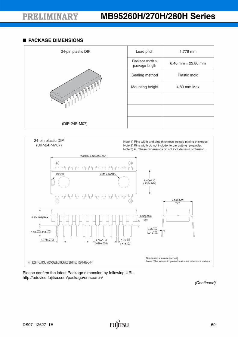
MB95260H/270H/280H Series
PACKAGE DIMENSIONS
Please confirm the latest Package dimension by following URL.http://edevice.fujitsu.com/package/en-search/
(Continued)
24-pin plastic DIP Lead pitch 1.778 mm
Package width ×package length
6.40 mm × 22.86 mm
Sealing method Plastic mold
Mounting height 4.80 mm Max
24-pin plastic DIP(DIP-24P-M07)
(DIP-24P-M07)
C 2008 FUJITSU MICROELECTRONICS LIMITED D24066S-c-1-1
#22.86±0.10(.900±.004)
INDEX
TYP.7.62(.300)
6.40±0.10(.252±.004)
BTM E-MARK
–0.04
+.004–.002.010
0.25+0.10
1 12
24 13
4.80(.189)MAX
+0.20–0.30
+.008–.0123.00 .118
1.778(.070)
(.039±.004)1.00±0.10
+0.09–0.04
+.004–.002.017
0.43
MIN0.50(.020)
Dimensions in mm (inches).Note: The values in parentheses are reference values
Note 1) Pins width and pins thickness include plating thickness.Note 2) Pins width do not include tie bar cutting remainder.Note 3) # : These dimensions do not include resin protrusion.
DS07–12627–1E 69
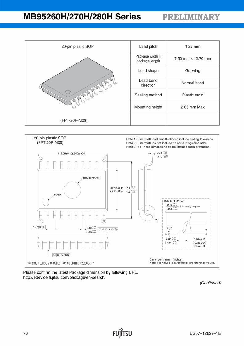
MB95260H/270H/280H Series
Please confirm the latest Package dimension by following URL.http://edevice.fujitsu.com/package/en-search/
(Continued)
20-pin plastic SOP Lead pitch 1.27 mm
Package width ×package length
7.50 mm × 12.70 mm
Lead shape Gullwing
Lead bend direction
Normal bend
Sealing method Plastic mold
Mounting height 2.65 mm Max
20-pin plastic SOP(FPT-20P-M09)
(FPT-20P-M09)
C 2008 FUJITSU MICROELECTRONICS LIMITED F20030S-c-1-1
Details of "A" part
INDEX
0.10(.004)
(.008±.004)0.20±0.10
–.007+.005
.099
–0.17+0.13
2.52(Mounting height)
0~8°
(Stand off)
0.80+0.47–0.30
.031+.019–.012
"A"
–.001+.003
.010
0.25+0.07–0.02#12.70±0.10(.500±.004)
1120
1.27(.050)
1 10
0.25(.010) M–0.05+0.09
0.40
.016+.004–.002
#7.50±0.10(.295±.004)
–0.20+0.40
10.2.402
+.016–.008
BTM E-MARK
Dimensions in mm (inches).Note: The values in parentheses are reference values.
Note 1) Pins width and pins thickness include plating thickness.Note 2) Pins width do not include tie bar cutting remainder.Note 3) # : These dimensions do not include resin protrusion.
70 DS07–12627–1E
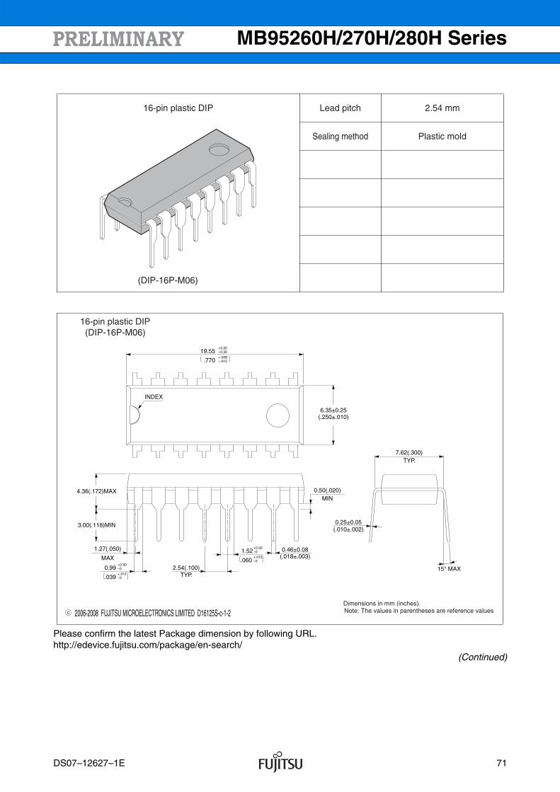
MB95260H/270H/280H Series
Please confirm the latest Package dimension by following URL.http://edevice.fujitsu.com/package/en-search/
(Continued)
16-pin plastic DIP Lead pitch 2.54 mm
Sealing method Plastic mold
16-pin plastic DIP(DIP-16P-M06)
(DIP-16P-M06)
C 2006-2008 FUJITSU MICROELECTRONICS LIMITED D16125S-c-1-2
0.25±0.05(.010±.002)
15° MAX
.770 –.012+.008
–0.30+0.20
19.55
INDEX
0.50(.020)MIN
TYP.2.54(.100)
(.018±.003)0.46±0.08
3.00(.118)MIN
4.36(.172)MAX
1.52
.060 –0+.012
–0+0.30
MAX
1.27(.050)
TYP.7.62(.300)
6.35±0.25(.250±.010)
.039
0.99+.012–0
+0.30–0
Dimensions in mm (inches).Note: The values in parentheses are reference values
DS07–12627–1E 71
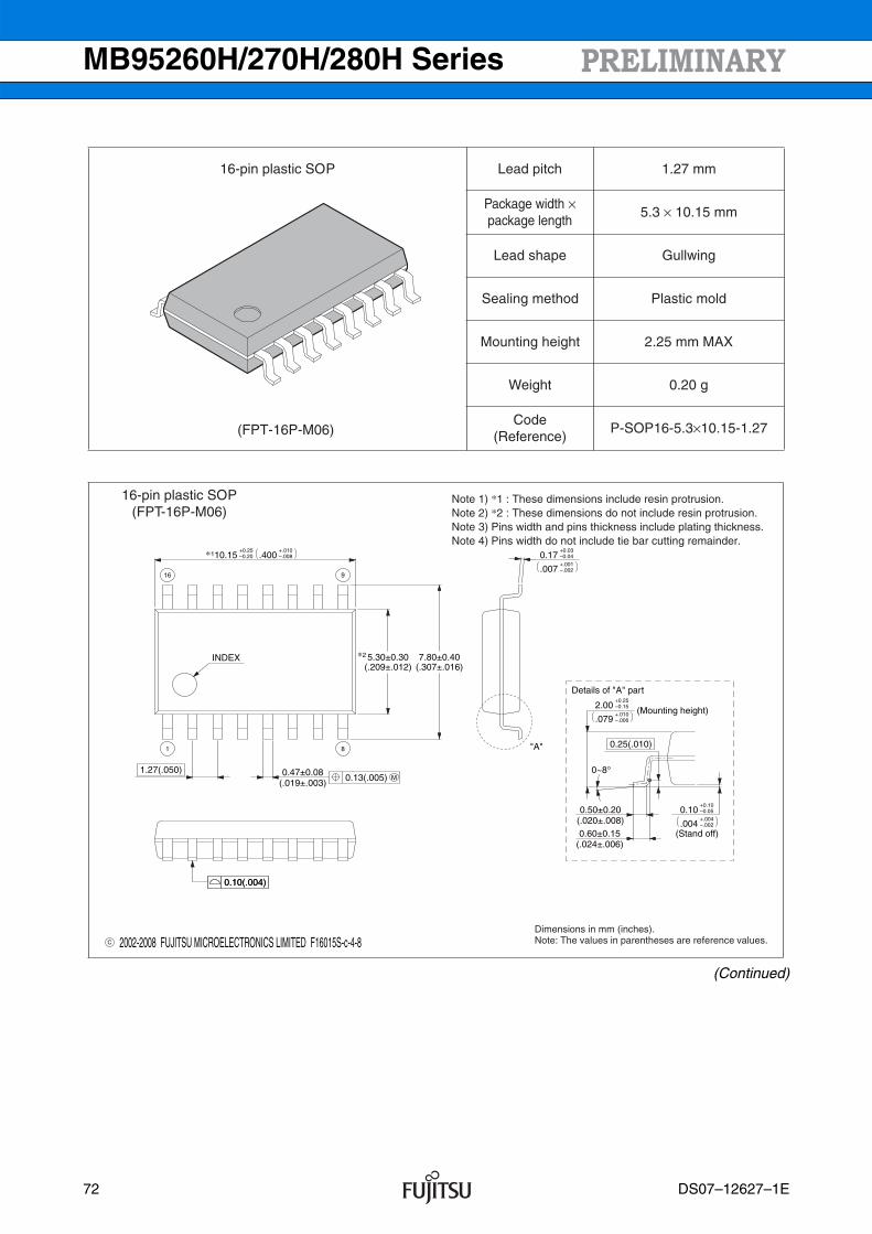
MB95260H/270H/280H Series
(Continued)
16-pin plastic SOP Lead pitch 1.27 mm
Package width ×package length
5.3 × 10.15 mm
Lead shape Gullwing
Sealing method Plastic mold
Mounting height 2.25 mm MAX
Weight 0.20 g
Code(Reference)
P-SOP16-5.3×10.15-1.27
16-pin plastic SOP(FPT-16P-M06)
(FPT-16P-M06)
C 2002-2008 FUJITSU MICROELECTRONICS LIMITED F16015S-c-4-8
0.13(.005) M
Details of "A" part
7.80±0.405.30±0.30(.209±.012) (.307±.016)
–.008+.010
–0.20+0.25
10.15
INDEX
1.27(.050)
0.10(.004)
1 8
916
0.47±0.08(.019±.003)
–0.04+0.03
0.17
.007+.001–.002
"A" 0.25(.010)
(Stand off)
0~8°
(Mounting height)2.00
+0.25–0.15
.079+.010–.006
0.50±0.20(.020±.008)0.60±0.15
(.024±.006)
0.10+0.10–0.05
–.002+.004
.004
.400*1
*2
0.10(.004)
Dimensions in mm (inches).Note: The values in parentheses are reference values.
Note 1) *1 : These dimensions include resin protrusion.Note 2) *2 : These dimensions do not include resin protrusion.Note 3) Pins width and pins thickness include plating thickness.Note 4) Pins width do not include tie bar cutting remainder.
72 DS07–12627–1E
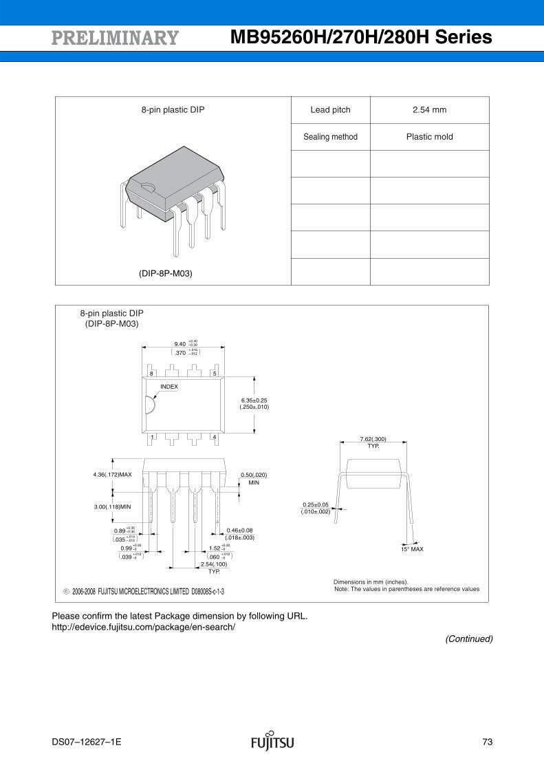
MB95260H/270H/280H Series
Please confirm the latest Package dimension by following URL.http://edevice.fujitsu.com/package/en-search/
(Continued)
8-pin plastic DIP Lead pitch 2.54 mm
Sealing method Plastic mold
8-pin plastic DIP(DIP-8P-M03)
(DIP-8P-M03)
C 2006-2008 FUJITSU MICROELECTRONICS LIMITED D08008S-c-1-3
0.25±0.05(.010±.002)
15° MAX
.370 –.012+.016
–0.30+0.40
9.40
(.250±.010)6.35±0.25
INDEX
1 4
8 5
0.50(.020)MIN
TYP.2.54(.100)
(.018±.003)0.46±0.08
3.00(.118)MIN
4.36(.172)MAX
1.52
.060 –0+.012
–0+0.30
–0
–00.99+0.30
+.012.039
.035
0.89+.014
+0.35
–.012
–0.30
TYP.7.62(.300)
Dimensions in mm (inches).Note: The values in parentheses are reference values
DS07–12627–1E 73
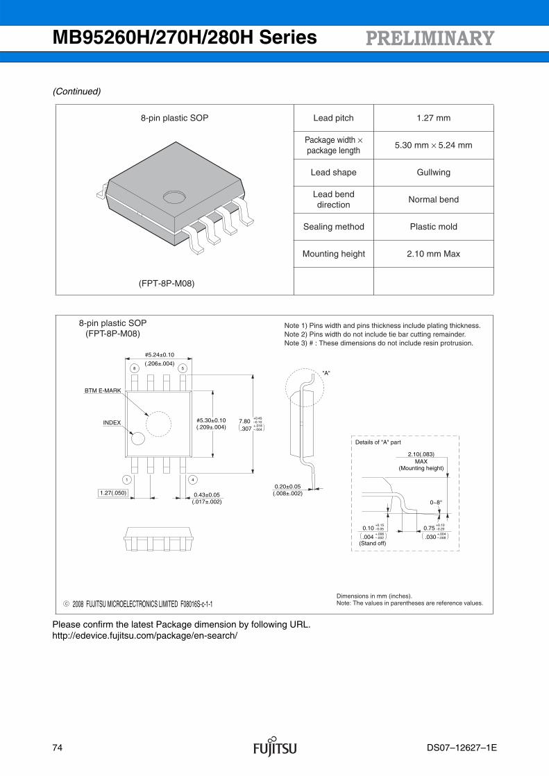
MB95260H/270H/280H Series
(Continued)
Please confirm the latest Package dimension by following URL.http://edevice.fujitsu.com/package/en-search/
8-pin plastic SOP Lead pitch 1.27 mm
Package width ×package length
5.30 mm × 5.24 mm
Lead shape Gullwing
Lead bend direction
Normal bend
Sealing method Plastic mold
Mounting height 2.10 mm Max
8-pin plastic SOP(FPT-8P-M08)
(FPT-8P-M08)
C 2008 FUJITSU MICROELECTRONICS LIMITED F08016S-c-1-1
Details of "A" part
#5.30±0.10(.209±.004)
INDEX
1.27(.050)
1 4
58
0.43±0.05(.017±.002)
"A"
(Stand off)
0~8°
(Mounting height)
2.10(.083)MAX
0.10+0.15–0.05
–.002+.006
.004
7.80+0.45–0.10+.018–.004.307
#5.24±0.10
(.206±.004)
BTM E-MARK
0.20±0.05(.008±.002)
+0.10–0.200.75
.030+.004–.008
Dimensions in mm (inches).Note: The values in parentheses are reference values.
Note 1) Pins width and pins thickness include plating thickness.Note 2) Pins width do not include tie bar cutting remainder.Note 3) # : These dimensions do not include resin protrusion.
74 DS07–12627–1E
MB95260H/270H/280H Series
MEMO
DS07–12627–1E 75
MB95260H/270H/280H Series
FUJITSU MICROELECTRONICS LIMITEDShinjuku Dai-Ichi Seimei Bldg., 7-1, Nishishinjuku 2-chome,Shinjuku-ku, Tokyo 163-0722, JapanTel: +81-3-5322-3347 Fax: +81-3-5322-3387http://jp.fujitsu.com/fml/en/
For further information please contact:
North and South AmericaFUJITSU MICROELECTRONICS AMERICA, INC.1250 E. Arques Avenue, M/S 333Sunnyvale, CA 94085-5401, U.S.A.Tel: +1-408-737-5600 Fax: +1-408-737-5999http://www.fma.fujitsu.com/
EuropeFUJITSU MICROELECTRONICS EUROPE GmbHPittlerstrasse 47, 63225 Langen, GermanyTel: +49-6103-690-0 Fax: +49-6103-690-122http://emea.fujitsu.com/microelectronics/
KoreaFUJITSU MICROELECTRONICS KOREA LTD.206 Kosmo Tower Building, 1002 Daechi-Dong,Gangnam-Gu, Seoul 135-280, Republic of KoreaTel: +82-2-3484-7100 Fax: +82-2-3484-7111http://kr.fujitsu.com/fmk/
Asia PacificFUJITSU MICROELECTRONICS ASIA PTE. LTD.151 Lorong Chuan,#05-08 New Tech Park 556741 SingaporeTel : +65-6281-0770 Fax : +65-6281-0220http://www.fmal.fujitsu.com/
FUJITSU MICROELECTRONICS SHANGHAI CO., LTD.Rm. 3102, Bund Center, No.222 Yan An Road (E),Shanghai 200002, ChinaTel : +86-21-6146-3688 Fax : +86-21-6335-1605http://cn.fujitsu.com/fmc/
FUJITSU MICROELECTRONICS PACIFIC ASIA LTD.10/F., World Commerce Centre, 11 Canton Road,Tsimshatsui, Kowloon, Hong KongTel : +852-2377-0226 Fax : +852-2376-3269http://cn.fujitsu.com/fmc/en/
Specifications are subject to change without notice. For further information please contact each office.
All Rights Reserved.The contents of this document are subject to change without notice. Customers are advised to consult with sales representatives before ordering.The information, such as descriptions of function and application circuit examples, in this document are presented solely for the purposeof reference to show examples of operations and uses of FUJITSU MICROELECTRONICS device; FUJITSU MICROELECTRONICSdoes not warrant proper operation of the device with respect to use based on such information. When you develop equipment incor-porating the device based on such information, you must assume any responsibility arising out of such use of the information. FUJITSU MICROELECTRONICS assumes no liability for any damages whatsoever arising out of the use of the information.Any information in this document, including descriptions of function and schematic diagrams, shall not be construed as license of the useor exercise of any intellectual property right, such as patent right or copyright, or any other right of FUJITSU MICROELECTRONICS orany third party or does FUJITSU MICROELECTRONICS warrant non-infringement of any third-party's intellectual property right or otherright by using such information. FUJITSU MICROELECTRONICS assumes no liability for any infringement of the intellectual propertyrights or other rights of third parties which would result from the use of information contained herein.The products described in this document are designed, developed and manufactured as contemplated for general use, including withoutlimitation, ordinary industrial use, general office use, personal use, and household use, but are not designed, developed and manufacturedas contemplated (1) for use accompanying fatal risks or dangers that, unless extremely high safety is secured, could have a serious effectto the public, and could lead directly to death, personal injury, severe physical damage or other loss (i.e., nuclear reaction control innuclear facility, aircraft flight control, air traffic control, mass transport control, medical life support system, missile launch control inweapon system), or (2) for use requiring extremely high reliability (i.e., submersible repeater and artificial satellite).Please note that FUJITSU MICROELECTRONICS will not be liable against you and/or any third party for any claims or damagesarising in connection with above-mentioned uses of the products.Any semiconductor devices have an inherent chance of failure. You must protect against injury, damage or loss from such failuresby incorporating safety design measures into your facility and equipment such as redundancy, fire protection, and prevention of over-current levels and other abnormal operating conditions.Exportation/release of any products described in this document may require necessary procedures in accordance with the regulationsof the Foreign Exchange and Foreign Trade Control Law of Japan and/or US export control laws.The company names and brand names herein are the trademarks or registered trademarks of their respective owners.
Edited: Sales Promotion Department