3-axis, digital magnetometerdlnmh9ip6v2uc.cloudfront.net/datasheets/sensors/magneto/...3-axis,...
TRANSCRIPT

Document Number: MAG3110Rev 5, 05/2011
Freescale SemiconductorData Sheet: Advance InformationAn Energy Efficient Solution by Freescale
This document contains information on a new product.Specifications and information herein are subject to change without notice.
© Freescale Semiconductor, Inc., 2011. All rights reserved.
3-Axis, Digital MagnetometerFreescale’s MAG3110 is a small, low-power, digital 3-axis magnetometer.
The device can be used in conjunction with a 3-axis accelerometer to produce orientation independent accurate compass heading information. It features a standard I2C serial interface output and smart embedded functions.
The MAG3110 is capable of measuring magnetic fields with an Output Data Rate (ODR) up to 80 Hz; these output data rates correspond to sample intervals from 12 ms to several seconds.
The MAG3110 is available in a plastic DFN package and it is guaranteed to operate over the extended temperature range of -40°C to +85°C.
Features• 1.95V to 3.6V Supply Voltage (VDD)• 1.62V to VDD IO Voltage (VDDIO)• Ultra Small 2 mm x 2 mm x 0.85 mm, 0.4 mm Pitch, 10 Pin Package• Full Scale Range ±1000 μT• Sensitivity of 0.10 μT• Noise down to 0.25 μT rms• Output Data Rates (ODR) up to 80 Hz • I2C digital output interface (operates up to 400 kHz Fast Mode)• 7-bit I2C address = 0x0E • Sampled Low Power Mode • RoHS compliant Applications• Electronic Compass• Dead-reckoning assistance for GPS backup• Location-based Services
ORDERING INFORMATIONPart Number Temperature Range Package Description Shipping
MAG3110FCR1 -40°C to +85°C DFN-10 Tape and Reel (1000)MAG3110FCR2 -40°C to +85°C DFN-10 Tape and Reel (4000)
10 PIN DFN2 mm x 2 mm x 0.85 mm
CASE 2154-01
MAG3110
MAG3110: 3-AXIS DIGITALMAGNETOMETER
Top and Bottom View
Top View
Pin Connections
Cap-AVDD
NCCap-R
GND
GNDINT1
SDA
VDDIOSCL
1
2
3
4
5
10
9
8
7
6
MAG3110

Application Notes for ReferenceThe following is a list of Freescale Application Notes written for the MAG3110:
• AN4247, Layout Recommendations for PCBs using a Magnetometer Sensor• AN4248, Implementing a Tilt-Compensated eCompass using Accelerometer and Magnetometer Sensors
1 Block Diagram and Pin Description
1.1 Block Diagram
Figure 1. Block Diagram
1.2 Pin Description
Figure 2. Pin Connections Figure 3. Measurement Coordinate System
Digital Signal
SDASCL
Processing andY-axis
Clock OscillatorReference
INT1
X-axis
Z-axis
MUX ADCControl
Trim Logic +Regulator VDD
VDDIO
(TOP VIEW)
X
Y
Z
1
(TOP VIEW)
Cap-AVDD
NCCap-R
GND
GNDINT1
SDA
VDDIOSCL
1
2
3
4
5
10
9
8
7
6
MAG3110
SensorsFreescale Semiconductor 2
MAG3110

1.3 Application CircuitThe device power is supplied through VDD line. Power supply decoupling capacitors (100 nF ceramic) should be placed as
near as possible to pins 1 and 2 of the device. VDDIO supplies power for the I/O pins SCL, SDA, and INT1.
The control signals SCL and SDA, are not tolerant of voltages more than VDDIO + 0.3 volts. If VDDIO is removed, the control signals SCL and SDA will clamp any logic signals with their internal ESD protection diodes.
Figure 4. Electrical Connection
Table 1. Pin Descriptions
Pin Name Function
1 Cap-A Bypass Cap for Internal Regulator
2 VDD Power Supply, 1.95V – 3.6V
3 NC Do not connect.
4 Cap-R Cap for Reset Pulse
5 GND GND
6 SDA I2C Serial Data (Write = 0x1C; Read = 0x1D)
7 SCL I2C Serial Clock
8 VDDIO Power for I/O Buffers, 1.65V - VDD
9 INT1 Interrupt - Active High Output
10 GND GND
SDA
VDDIO
1
2
3
4
5
10
9
8
7
6
MAG3110(Top View)
100 nF
1 μF
VDD
100 nF100 nF
SCL
INT1
4.7K100 nF
4.7K
Sensors3 Freescale Semiconductor
MAG3110
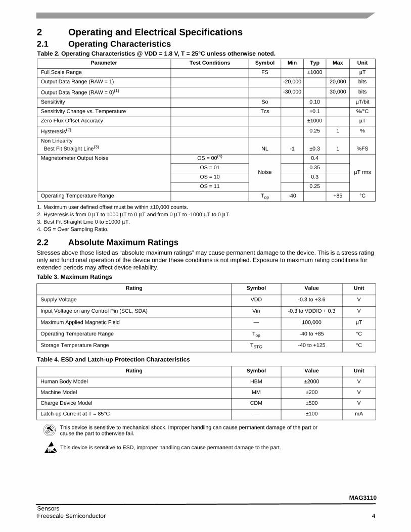
2 Operating and Electrical Specifications2.1 Operating Characteristics
2.2 Absolute Maximum RatingsStresses above those listed as “absolute maximum ratings” may cause permanent damage to the device. This is a stress rating only and functional operation of the device under these conditions is not implied. Exposure to maximum rating conditions for extended periods may affect device reliability.
Table 2. Operating Characteristics @ VDD = 1.8 V, T = 25°C unless otherwise noted.Parameter Test Conditions Symbol Min Typ Max Unit
Full Scale Range FS ±1000 µT
Output Data Range (RAW = 1) -20,000 20,000 bits
Output Data Range (RAW = 0)(1)
1. Maximum user defined offset must be within ±10,000 counts.
-30,000 30,000 bits
Sensitivity So 0.10 µT/bit
Sensitivity Change vs. Temperature Tcs ±0.1 %/°C
Zero Flux Offset Accuracy ±1000 µT
Hysteresis(2)
2. Hysteresis is from 0 μT to 1000 μT to 0 μT and from 0 μT to -1000 μT to 0 μT.
0.25 1 %
Non Linearity Best Fit Straight Line(3)
3. Best Fit Straight Line 0 to ±1000 μT.
NL -1 ±0.3 1 %FS
Magnetometer Output Noise OS = 00(4)
4. OS = Over Sampling Ratio.
Noise
0.4
µT rmsOS = 01 0.35
OS = 10 0.3
OS = 11 0.25
Operating Temperature Range Top -40 +85 °C
Table 3. Maximum Ratings
Rating Symbol Value Unit
Supply Voltage VDD -0.3 to +3.6 V
Input Voltage on any Control Pin (SCL, SDA) Vin -0.3 to VDDIO + 0.3 V
Maximum Applied Magnetic Field — 100,000 µT
Operating Temperature Range Top -40 to +85 °C
Storage Temperature Range TSTG -40 to +125 °C
Table 4. ESD and Latch-up Protection Characteristics
Rating Symbol Value Unit
Human Body Model HBM ±2000 V
Machine Model MM ±200 V
Charge Device Model CDM ±500 V
Latch-up Current at T = 85°C — ±100 mA
This device is sensitive to mechanical shock. Improper handling can cause permanent damage of the part or cause the part to otherwise fail.
This device is sensitive to ESD, improper handling can cause permanent damage to the part.
SensorsFreescale Semiconductor 4
MAG3110
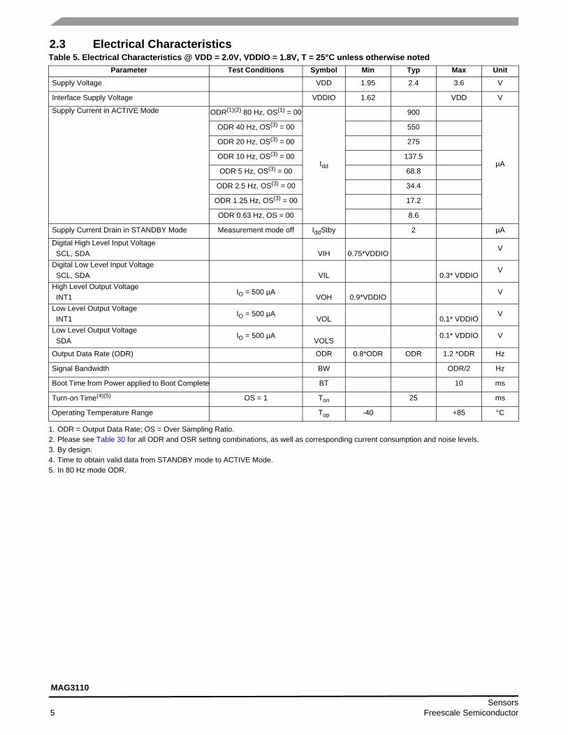
2.3 Electrical CharacteristicsTable 5. Electrical Characteristics @ VDD = 2.0V, VDDIO = 1.8V, T = 25°C unless otherwise noted
Parameter Test Conditions Symbol Min Typ Max Unit
Supply Voltage VDD 1.95 2.4 3.6 V
Interface Supply Voltage VDDIO 1.62 VDD V
Supply Current in ACTIVE Mode ODR(1)(2) 80 Hz, OS(1) = 00
1. ODR = Output Data Rate; OS = Over Sampling Ratio.2. Please see Table 30 for all ODR and OSR setting combinations, as well as corresponding current consumption and noise levels.
Idd
900
µA
ODR 40 Hz, OS(3) = 00
3. By design.
550
ODR 20 Hz, OS(3) = 00 275
ODR 10 Hz, OS(3) = 00 137.5
ODR 5 Hz, OS(3) = 00 68.8
ODR 2.5 Hz, OS(3) = 00 34.4
ODR 1.25 Hz, OS(3) = 00 17.2
ODR 0.63 Hz, OS = 00 8.6
Supply Current Drain in STANDBY Mode Measurement mode off IddStby 2 µA
Digital High Level Input VoltageSCL, SDA VIH 0.75*VDDIO
V
Digital Low Level Input Voltage SCL, SDA VIL 0.3* VDDIO
V
High Level Output VoltageINT1
IO = 500 µAVOH 0.9*VDDIO
V
Low Level Output Voltage INT1
IO = 500 µAVOL 0.1* VDDIO
V
Low Level Output VoltageSDA
IO = 500 µAVOLS
0.1* VDDIO V
Output Data Rate (ODR) ODR 0.8*ODR ODR 1.2 *ODR Hz
Signal Bandwidth BW ODR/2 Hz
Boot Time from Power applied to Boot Complete BT 10 ms
Turn-on Time(4)(5)
4. Time to obtain valid data from STANDBY mode to ACTIVE Mode.5. In 80 Hz mode ODR.
OS = 1 Ton 25 ms
Operating Temperature Range Top -40 +85 °C
Sensors5 Freescale Semiconductor
MAG3110
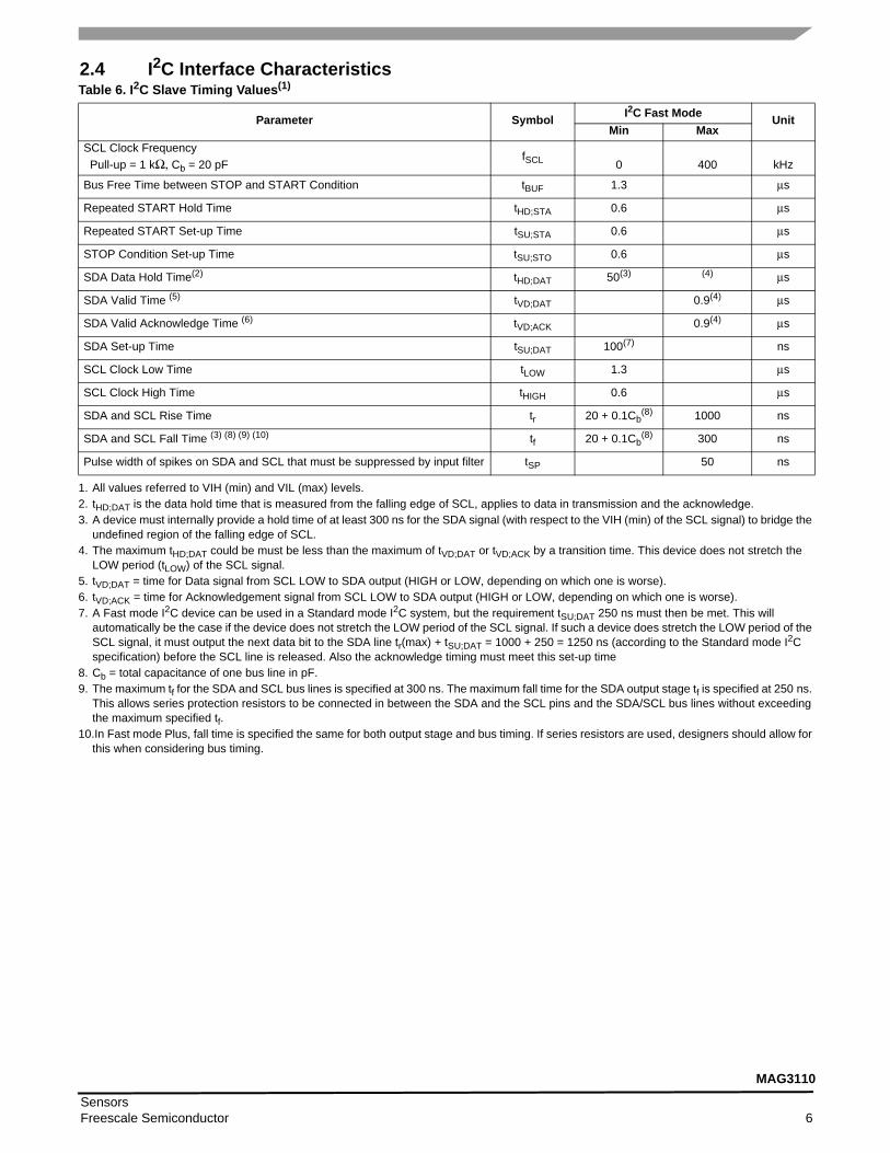
2.4 I2C Interface CharacteristicsTable 6. I2C Slave Timing Values(1)
1. All values referred to VIH (min) and VIL (max) levels.
Parameter Symbol I2C Fast Mode UnitMin Max
SCL Clock FrequencyPull-up = 1 kΩ, Cb = 20 pF
fSCL 0 400 kHz
Bus Free Time between STOP and START Condition tBUF 1.3 μs
Repeated START Hold Time tHD;STA 0.6 μs
Repeated START Set-up Time tSU;STA 0.6 μs
STOP Condition Set-up Time tSU;STO 0.6 μs
SDA Data Hold Time(2)
2. tHD;DAT is the data hold time that is measured from the falling edge of SCL, applies to data in transmission and the acknowledge.
tHD;DAT 50(3)
3. A device must internally provide a hold time of at least 300 ns for the SDA signal (with respect to the VIH (min) of the SCL signal) to bridge the undefined region of the falling edge of SCL.
(4)
4. The maximum tHD;DAT could be must be less than the maximum of tVD;DAT or tVD;ACK by a transition time. This device does not stretch the LOW period (tLOW) of the SCL signal.
μs
SDA Valid Time (5)
5. tVD;DAT = time for Data signal from SCL LOW to SDA output (HIGH or LOW, depending on which one is worse).
tVD;DAT 0.9(4) μs
SDA Valid Acknowledge Time (6)
6. tVD;ACK = time for Acknowledgement signal from SCL LOW to SDA output (HIGH or LOW, depending on which one is worse).
tVD;ACK 0.9(4) μs
SDA Set-up Time tSU;DAT 100(7)
7. A Fast mode I2C device can be used in a Standard mode I2C system, but the requirement tSU;DAT 250 ns must then be met. This will automatically be the case if the device does not stretch the LOW period of the SCL signal. If such a device does stretch the LOW period of the SCL signal, it must output the next data bit to the SDA line tr(max) + tSU;DAT = 1000 + 250 = 1250 ns (according to the Standard mode I2C specification) before the SCL line is released. Also the acknowledge timing must meet this set-up time
ns
SCL Clock Low Time tLOW 1.3 μs
SCL Clock High Time tHIGH 0.6 μs
SDA and SCL Rise Time tr 20 + 0.1Cb(8) 1000 ns
SDA and SCL Fall Time (3) (8) (9) (10)
8. Cb = total capacitance of one bus line in pF.9. The maximum tf for the SDA and SCL bus lines is specified at 300 ns. The maximum fall time for the SDA output stage tf is specified at 250 ns.
This allows series protection resistors to be connected in between the SDA and the SCL pins and the SDA/SCL bus lines without exceeding the maximum specified tf.
10.In Fast mode Plus, fall time is specified the same for both output stage and bus timing. If series resistors are used, designers should allow for this when considering bus timing.
tf 20 + 0.1Cb(8) 300 ns
Pulse width of spikes on SDA and SCL that must be suppressed by input filter tSP 50 ns
SensorsFreescale Semiconductor 6
MAG3110
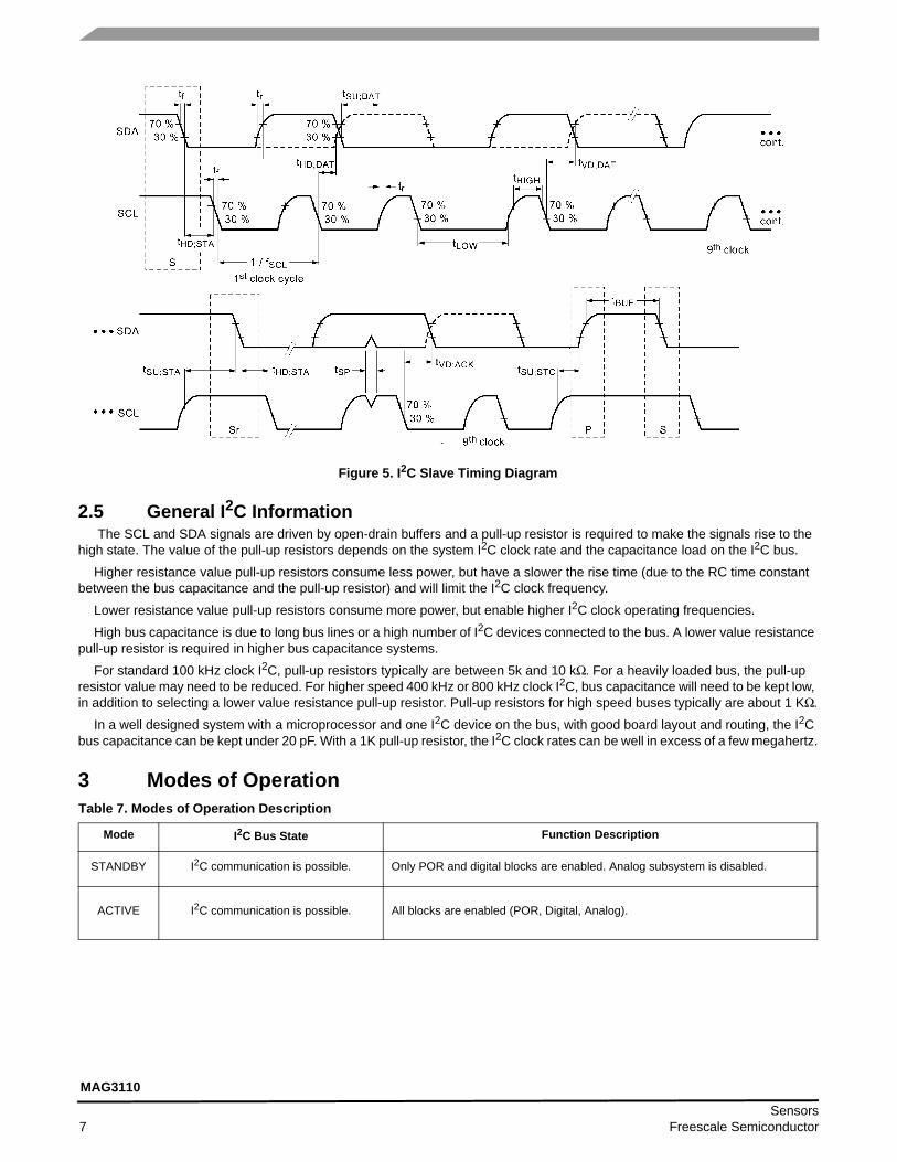
Figure 5. I2C Slave Timing Diagram
2.5 General I2C Information The SCL and SDA signals are driven by open-drain buffers and a pull-up resistor is required to make the signals rise to the
high state. The value of the pull-up resistors depends on the system I2C clock rate and the capacitance load on the I2C bus.
Higher resistance value pull-up resistors consume less power, but have a slower the rise time (due to the RC time constant between the bus capacitance and the pull-up resistor) and will limit the I2C clock frequency.
Lower resistance value pull-up resistors consume more power, but enable higher I2C clock operating frequencies.
High bus capacitance is due to long bus lines or a high number of I2C devices connected to the bus. A lower value resistance pull-up resistor is required in higher bus capacitance systems.
For standard 100 kHz clock I2C, pull-up resistors typically are between 5k and 10 kΩ. For a heavily loaded bus, the pull-up resistor value may need to be reduced. For higher speed 400 kHz or 800 kHz clock I2C, bus capacitance will need to be kept low, in addition to selecting a lower value resistance pull-up resistor. Pull-up resistors for high speed buses typically are about 1 KΩ.
In a well designed system with a microprocessor and one I2C device on the bus, with good board layout and routing, the I2C bus capacitance can be kept under 20 pF. With a 1K pull-up resistor, the I2C clock rates can be well in excess of a few megahertz.
3 Modes of OperationTable 7. Modes of Operation Description
Mode I2C Bus State Function Description
STANDBY I2C communication is possible. Only POR and digital blocks are enabled. Analog subsystem is disabled.
ACTIVE I2C communication is possible. All blocks are enabled (POR, Digital, Analog).
Sensors7 Freescale Semiconductor
MAG3110
4 FunctionalityMAG3110 is a small low-power, digital output, 3-axis linear magnetometer packaged in a 10 pin DFN. The device contains a
magnetic transducer for sensing and an ASIC for control and digital I2C communications.
4.1 I2C Serial InterfaceCommunication with the MAG3110 takes place over an I2C bus. The MAG3110 also has an interrupt signal indicating that new
magnetic data readings are available. Interrupt driven sampling allows operation without the overhead of software polling.
4.2 Factory CalibrationMAG3110 is factory calibrated for sensitivity and temperature coefficient. All factory calibration coefficients are applied
automatically by the MAG3110 ASIC before the magnetic field readings are written to registers 0x01 to 0x06 (see section 5). There is no need for the user to apply the calibration correction in the software and the calibration coefficients are not therefore accessible to the user.
The offset registers in the addresses 0x09 to 0x0E are not a factory calibration offset but allow the user to define a hard iron offset which can be automatically subtracted from the magnetic field readings (see section 4.3.3).
4.3 Digital Interface
There are two signals associated with the I2C bus: the Serial Clock Line (SCL) and the Serial Data line (SDA). External pull-up resistors (connected to VDDIO) are needed for SDA and SCL. When the bus is free, both lines are high. The I2C interface is compliant with Fast mode (400 kHz), and Normal mode (100 kHz) I2C standards.
4.3.1 General I2C OperationI2C is an asynchronous, open collector driven, addressed and packetized serial bus interface. It is capable of supporting
multiple masters and multiple slave devices on the same bus. I2C uses two bi-directional lines, the serial clock line or SCL and the serial data line or SDA. Pull-up resistors are required on both lines.
An I2C transaction starts with a start condition (START) and ends with a stop condition (STOP). A START condition is defined as a HIGH to LOW transition on the data line while the clock line is held HIGH. A STOP condition is defined as a LOW to HIGH transition on the data line while the clock line is held HIGH. At all other times, the data line can only change state when the clock line is low. If the data line changes state when the clock is high, the I2C transaction is aborted and the new start or stop condition is recognized.
After START has been transmitted by the master, the bus is considered busy. The next byte of data transmitted after START condition is the slave address in the first 7 bits, and the eighth bit is the Read/Write (R/W) bit (read = 1, write = 0). The R/W bit determines whether the I2C master intends on receiving data from the slave – Read mode or intends to transmit data to the slave – Write mode. When an address is sent, each device on the I2C bus compares the first 7 bits after a start condition with its own internal address. If the address matches, the device considers itself addressed by the Master and continues to respond. If the address does not match, the device ignores further bus activity until the next start condition happens.
The ninth bit (clock pulse), following each I2C byte is for the acknowledge (ACK) bit. The master releases the SDA line during the ACK period. Because of the pull-up resistor, the data line will tend to float high. To signal ACK back to the master, the slave must then pull the data line low during this clock period.
The number of bytes per transfer can be unlimited. If a receiving device can't accept another complete byte of data until it has performed some other function, it can hold the clock line, SCL, low to force the transmitter into a wait state. Data transfer only continues when the receiver is ready for another byte and releases the data line. This delay action is called clock stretching. The MAG3110 device does clock stretching.
A data transfer is always terminated by a STOP.
The MAG3110 I2C 7-bit device address is 0x0E. In I2C practice, the device address is shifted left by one bit field and a read/ write bit is set in the lowest bit position. The I2C 8-bit write address is therefore 0x1C and the read address 0x1D.
Table 8. Serial Interface Pin Description
Pin Name Pin Description
VDDIO IO voltage
SCL I2C Serial Clock
SDA I2C Serial Data
INT Data ready interrupt pin
SensorsFreescale Semiconductor 8
MAG3110
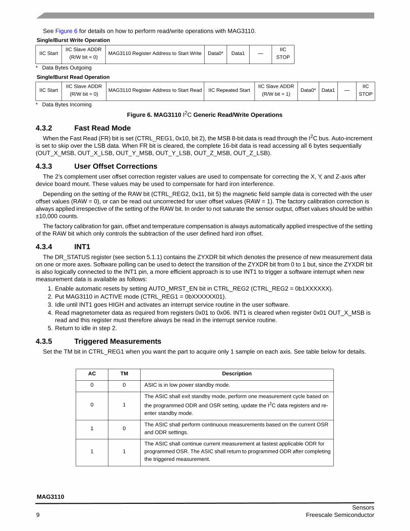
See Figure 6 for details on how to perform read/write operations with MAG3110.
* Data Bytes Outgoing
* Data Bytes Incoming
Figure 6. MAG3110 I2C Generic Read/Write Operations
4.3.2 Fast Read ModeWhen the Fast Read (FR) bit is set (CTRL_REG1, 0x10, bit 2), the MSB 8-bit data is read through the I2C bus. Auto-increment
is set to skip over the LSB data. When FR bit is cleared, the complete 16-bit data is read accessing all 6 bytes sequentially (OUT_X_MSB, OUT_X_LSB, OUT_Y_MSB, OUT_Y_LSB, OUT_Z_MSB, OUT_Z_LSB).
4.3.3 User Offset CorrectionsThe 2’s complement user offset correction register values are used to compensate for correcting the X, Y, and Z-axis after
device board mount. These values may be used to compensate for hard iron interference.
Depending on the setting of the RAW bit (CTRL_REG2, 0x11, bit 5) the magnetic field sample data is corrected with the user offset values (RAW = 0), or can be read out uncorrected for user offset values (RAW = 1). The factory calibration correction is always applied irrespective of the setting of the RAW bit. In order to not saturate the sensor output, offset values should be within ±10,000 counts.
The factory calibration for gain, offset and temperature compensation is always automatically applied irrespective of the setting of the RAW bit which only controls the subtraction of the user defined hard iron offset.
4.3.4 INT1The DR_STATUS register (see section 5.1.1) contains the ZYXDR bit which denotes the presence of new measurement data
on one or more axes. Software polling can be used to detect the transition of the ZYXDR bit from 0 to 1 but, since the ZYXDR bit is also logically connected to the INT1 pin, a more efficient approach is to use INT1 to trigger a software interrupt when new measurement data is available as follows:
1. Enable automatic resets by setting AUTO_MRST_EN bit in CTRL_REG2 (CTRL_REG2 = 0b1XXXXXX).2. Put MAG3110 in ACTIVE mode (CTRL_REG1 = 0bXXXXXX01).3. Idle until INT1 goes HIGH and activates an interrupt service routine in the user software.4. Read magnetometer data as required from registers 0x01 to 0x06. INT1 is cleared when register 0x01 OUT_X_MSB is
read and this register must therefore always be read in the interrupt service routine.5. Return to idle in step 2.
4.3.5 Triggered MeasurementsSet the TM bit in CTRL_REG1 when you want the part to acquire only 1 sample on each axis. See table below for details.
Single/Burst Write Operation
IIC StartIIC Slave ADDR
(R/W bit = 0)MAG3110 Register Address to Start Write Data0* Data1 —
IIC STOP
Single/Burst Read Operation
IIC StartIIC Slave ADDR
(R/W bit = 0)MAG3110 Register Address to Start Read IIC Repeated Start
IIC Slave ADDR(R/W bit = 1)
Data0* Data1 —IIC
STOP
AC TM Description
0 0 ASIC is in low power standby mode.
0 1The ASIC shall exit standby mode, perform one measurement cycle based on
the programmed ODR and OSR setting, update the I2C data registers and re- enter standby mode.
1 0The ASIC shall perform continuous measurements based on the current OSR and ODR settings.
1 1The ASIC shall continue current measurement at fastest applicable ODR for programmed OSR. The ASIC shall return to programmed ODR after completing the triggered measurement.
Sensors9 Freescale Semiconductor
MAG3110

4.3.6 MAG3110 Setup ExamplesContinuous Measurements with ODR = 80 Hz, OSR = 1
1. Enable automatic resets by setting bit AUTO_MRST_EN in CTRL_REG2. (CTRL_REG2 = 0x80)2. Put MAG3110 in active mode 80 Hz with OSR = 1 by writing 0x01 to CTRL_REG1 (CTRL_REG1 = 0x01)3. At this point it is possible to sync with MAG3110 utilizing INT1 pin or using polling of the DR_STATUS register as
explained in section 4.3.4.
Continuous Measurements with ODR = 0.63 Hz, OSR = 21. Enable automatic resets by setting bit AUTO_MRST_EN in CTRL_REG2. (CTRL_REG2 = 0x80)2. Put MAG3110 in active mode 0.63 Hz with OSR = 2 by writing 0xC9 to CTRL_REG1 (CTRL_REG1 = 0xC9)3. At this point, it is possible to sync with MAG3110 utilizing INT1 pin or using polling of the DR_STATUS register as
explained in section 4.3.4.
Triggered Measurements with ODR = 10 Hz, OSR = 81. Enable automatic resets by setting bit AUTO_MRST_EN in CTRL_REG2. (CTRL_REG2 = 0x80)2. Initiate a triggered measurement by writing 0b00011010 to CTRL_REG1 (CTRL_REG1 = 0b00011010).3. MAG3110 will acquire the triggered measurement and go back into STANDBY mode. It is possible at this point to sync
on INT1 or resort to polling of DR_STATUS register to read acquired data out of MAG3110.4. Go to step 2 based on application needs.
5 Register DescriptionsTable 9. Register Address Map
Name Type RegisterAddress
Auto-IncrementAddress (Fast Read)(1)
1. Fast Read mode for quickly reading the Most Significant Bytes (MSB) of the sampled data.
Default Value Comment
DR_STATUS(2)
2. Register contents are preserved when transitioning from “ACTIVE” to “STANDBY” mode.
R 0x00 0x01 0000 0000 Data ready status per axis
OUT_X_MSB(2) R 0x01 0x02 (0x03) data Bits [15:8] of X measurement
OUT_X_LSB(2) R 0x02 0x03 data Bits [7:0] of X measurement
OUT_Y_MSB(2) R 0x03 0x04 (0x05) data Bits [15:8] of Y measurement
OUT_Y_LSB(2) R 0x04 0x05 data Bits [7:0] of Y measurement
OUT_Z_MSB(2) R 0x05 0x06 (0x07) data Bits [15:8] of Z measurement
OUT_Z_LSB(2) R 0x06 0x07 data Bits [7:0] of Z measurement
WHO_AM_I(2) R 0x07 0x08 0xC4 Device ID Number
SYSMOD(2) R 0x08 0x09 data Current System Mode
OFF_X_MSB R/W 0X09 0x0A 0000 0000 Bits [14:7] of user X offset
OFF_X_LSB R/W 0X0A 0X0B 0000 0000 Bits [6:0] of user X offset
OFF_Y_MSB R/W 0X0B 0X0C 0000 0000 Bits [14:7] of user Y offset
OFF_Y_LSB R/W 0X0C 0X0D 0000 0000 Bits [6:0] of user Y offset
OFF_Z_MSB R/W 0X0D 0X0E 0000 0000 Bits [14:7] of user Z offset
OFF_Z_LSB R/W 0X0E 0X0F 0000 0000 Bits [6:0] of user Z offset
DIE_TEMP(2) R 0X0F 0X10 data Temperature, signed 8 bits in °C
CTRL_REG1(3)
3. Modification of this register’s contents can only occur when device is “STANDBY” mode, except the TM and AC bit fields in CTRL_REG1 register.
R/W 0X10 0X11 0000 0000 Operation modes
CTRL_REG2(3) R/W 0X11 0x12 0000 0000 Operation modes
SensorsFreescale Semiconductor 10
MAG3110

5.1 Sensor Status5.1.1 DR_STATUS (0x00) Data Ready Status
This read-only status register provides the acquisition status information on a per-sample basis, and reflects real-time updates to the OUT_X, OUT_Y, and OUT_Z registers.
ZYXOW is set to 1 whenever new data is acquired before completing the retrieval of the previous set. This event occurs when the content of at least one data register (i.e. OUT_X, OUT_Y, OUT_Z) has been overwritten. ZYXOW is cleared when the high-bytes of the data (OUT_X_MSB, OUT_Y_MSB, OUT_Z_MSB) of all active channels are read.ZOW is set to 1 whenever new Z-axis acquisition is completed before the retrieval of the previous data. When this occurs the previous data is overwritten. ZOW is cleared any time OUT_Z_MSB register is read.YOW is set to 1 whenever new Y-axis acquisition is completed before the retrieval of the previous data. When this occurs the previous data is overwritten. YOW is cleared any time OUT_Y_MSB register is read.XOW is set to 1 whenever new X-axis acquisition is completed before the retrieval of the previous data. When this occurs the previous data is overwritten. XOW is cleared any time OUT_X_MSB register is read.ZYXDR signals that new acquisition for any of the enabled channels is available. ZYXDR is cleared when the high-bytes of the data (OUT_X_MSB, OUT_Y_MSB, OUT_Z_MSB) of all the enabled channels are read.ZDR is set to 1 whenever new Z-axis data acquisition is completed. ZDR is cleared any time OUT_Z_MSB register is read. YDR is set to 1 whenever new Y-axis data acquisition is completed. YDR is cleared any time OUT_Y_MSB register is read. XDR is set to 1 whenever new X-axis data acquisition is completed. XDR is cleared any time OUT_X_MSB register is read.
Table 10. DR_STATUS RegisterBit 7 Bit 6 Bit 5 Bit 4 Bit 3 Bit 2 Bit 1 Bit 0
ZYXOW ZOW YOW XOW ZYXDR ZDR YDR XDR
Table 11. DR_STATUS Descriptions
ZYXOWX, Y, Z-axis Data Overwrite. Default value: 0. 0: No data overwrite has occurred. 1: Previous X or Y or Z data was overwritten by new X or Y or Z data before it was completely read.
ZOWZ-axis Data Overwrite. Default value: 0. 0: No data overwrite has occurred. 1: Previous Z-axis data was overwritten by new Z-axis data before it was read.
YOWY-axis Data Overwrite. Default value: 0. 0: No data overwrite has occurred. 1: Previous Y-axis data was overwritten by new Y-axis data before it was read.
XOWX-axis Data Overwrite. Default value: 0 0: No data overwrite has occurred.1: Previous X-axis data was overwritten by new X-axis data before it was read.
ZYXDRX or Y or Z-axis new Data Ready. Default value: 0. 0: No new set of data ready. 1: New set of data is ready.
ZDRZ-axis new Data Available. Default value: 0. 0: No new Z-axis data is ready.1: New Z-axis data is ready.
YDRZ-axis new Data Available. Default value: 0. 0: No new Y-axis data is ready.1: New Y-axis data is ready.
XDRZ-axis new Data Available. Default value: 0. 0: No new X-axis data is ready.1: New X-axis data is ready.
Sensors11 Freescale Semiconductor
MAG3110
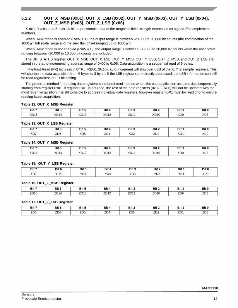
5.1.2 OUT_X_MSB (0x01), OUT_X_LSB (0x02), OUT_Y_MSB (0x03), OUT_Y_LSB (0x04), OUT_Z_MSB (0x05), OUT_Z_LSB (0x06)
X-axis, Y-axis, and Z-axis 16-bit output sample data of the magnetic field strength expressed as signed 2's complement numbers.
When RAW mode is enabled (RAW = 1), the output range is between -20,000 to 20,000 bit counts (the combination of the 1000 μT full scale range and the zero flux offset ranging up to 1000 μT).
When RAW mode is not enabled (RAW = 0), the output range is between -30,000 to 30,000 bit counts when the user offset ranging between -10,000 to 10,000 bit counts are included
The DR_STATUS register, OUT_X_MSB, OUT_X_LSB, OUT_Y_MSB, OUT_Y_LSB, OUT_Z_MSB, and OUT_Z_LSB are stored in the auto-incrementing address range of 0x00 to 0x06. Data acquisition is a sequential read of 6 bytes.
If the Fast Read (FR) bit is set in CTRL_REG1 (0x10), auto-increment will skip over LSB of the X, Y, Z sample registers. This will shorten the data acquisition from 6 bytes to 3 bytes. If the LSB registers are directly addressed, the LSB information can still be read regardless of FR bit setting.
The preferred method for reading data registers is the burst read method where the user application acquires data sequentially starting from register 0x01. If register 0x01 is not read, the rest of the data registers (0x02 - 0x06) will not be updated with the most recent acquisition. It is still possible to address individual data registers, however register 0x01 must be read prior to ensure reading latest acquisition.
Table 12. OUT_X_MSB RegisterBit 7 Bit 6 Bit 5 Bit 4 Bit 3 Bit 2 Bit 1 Bit 0XD15 XD14 XD13 XD12 XD11 XD10 XD9 XD8
Table 13. OUT_X_LSB RegisterBit 7 Bit 6 Bit 5 Bit 4 Bit 3 Bit 2 Bit 1 Bit 0XD7 XD6 XD5 XD4 XD3 XD2 XD1 XD0
Table 14. OUT_Y_MSB RegisterBit 7 Bit 6 Bit 5 Bit 4 Bit 3 Bit 2 Bit 1 Bit 0YD15 YD14 YD13 YD12 YD11 YD10 YD9 YD8
Table 15. OUT_Y_LSB RegisterBit 7 Bit 6 Bit 5 Bit 4 Bit 3 Bit 2 Bit 1 Bit 0YD7 YD6 YD5 YD4 YD3 YD2 YD1 YD0
Table 16. OUT_Z_MSB RegisterBit 7 Bit 6 Bit 5 Bit 4 Bit 3 Bit 2 Bit 1 Bit 0ZD15 ZD14 ZD13 ZD12 ZD11 ZD10 ZD9 ZD8
Table 17. OUT_Z_LSB RegisterBit 7 Bit 6 Bit 5 Bit 4 Bit 3 Bit 2 Bit 1 Bit 0ZD6 ZD6 ZD5 ZD4 ZD3 ZD2 ZD1 ZD0
SensorsFreescale Semiconductor 12
MAG3110
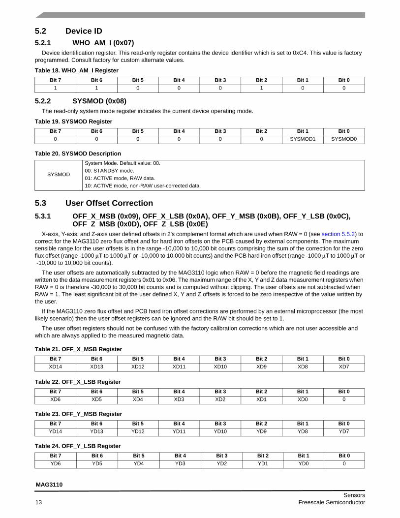
5.2 Device ID5.2.1 WHO_AM_I (0x07)
Device identification register. This read-only register contains the device identifier which is set to 0xC4. This value is factory programmed. Consult factory for custom alternate values.
5.2.2 SYSMOD (0x08)The read-only system mode register indicates the current device operating mode.
5.3 User Offset Correction5.3.1 OFF_X_MSB (0x09), OFF_X_LSB (0x0A), OFF_Y_MSB (0x0B), OFF_Y_LSB (0x0C),
OFF_Z_MSB (0x0D), OFF_Z_LSB (0x0E)X-axis, Y-axis, and Z-axis user defined offsets in 2's complement format which are used when RAW = 0 (see section 5.5.2) to
correct for the MAG3110 zero flux offset and for hard iron offsets on the PCB caused by external components. The maximum sensible range for the user offsets is in the range -10,000 to 10,000 bit counts comprising the sum of the correction for the zero flux offset (range -1000 μT to 1000 μT or -10,000 to 10,000 bit counts) and the PCB hard iron offset (range -1000 μT to 1000 μT or -10,000 to 10,000 bit counts).
The user offsets are automatically subtracted by the MAG3110 logic when RAW = 0 before the magnetic field readings are written to the data measurement registers 0x01 to 0x06. The maximum range of the X, Y and Z data measurement registers when RAW = 0 is therefore -30,000 to 30,000 bit counts and is computed without clipping. The user offsets are not subtracted when RAW = 1. The least significant bit of the user defined X, Y and Z offsets is forced to be zero irrespective of the value written by the user.
If the MAG3110 zero flux offset and PCB hard iron offset corrections are performed by an external microprocessor (the most likely scenario) then the user offset registers can be ignored and the RAW bit should be set to 1.
The user offset registers should not be confused with the factory calibration corrections which are not user accessible and which are always applied to the measured magnetic data.
Table 18. WHO_AM_I RegisterBit 7 Bit 6 Bit 5 Bit 4 Bit 3 Bit 2 Bit 1 Bit 0
1 1 0 0 0 1 0 0
Table 19. SYSMOD RegisterBit 7 Bit 6 Bit 5 Bit 4 Bit 3 Bit 2 Bit 1 Bit 0
0 0 0 0 0 0 SYSMOD1 SYSMOD0
Table 20. SYSMOD Description
SYSMOD
System Mode. Default value: 00.00: STANDBY mode.01: ACTIVE mode, RAW data.10: ACTIVE mode, non-RAW user-corrected data.
Table 21. OFF_X_MSB RegisterBit 7 Bit 6 Bit 5 Bit 4 Bit 3 Bit 2 Bit 1 Bit 0XD14 XD13 XD12 XD11 XD10 XD9 XD8 XD7
Table 22. OFF_X_LSB RegisterBit 7 Bit 6 Bit 5 Bit 4 Bit 3 Bit 2 Bit 1 Bit 0XD6 XD5 XD4 XD3 XD2 XD1 XD0 0
Table 23. OFF_Y_MSB RegisterBit 7 Bit 6 Bit 5 Bit 4 Bit 3 Bit 2 Bit 1 Bit 0YD14 YD13 YD12 YD11 YD10 YD9 YD8 YD7
Table 24. OFF_Y_LSB RegisterBit 7 Bit 6 Bit 5 Bit 4 Bit 3 Bit 2 Bit 1 Bit 0YD6 YD5 YD4 YD3 YD2 YD1 YD0 0
Sensors13 Freescale Semiconductor
MAG3110
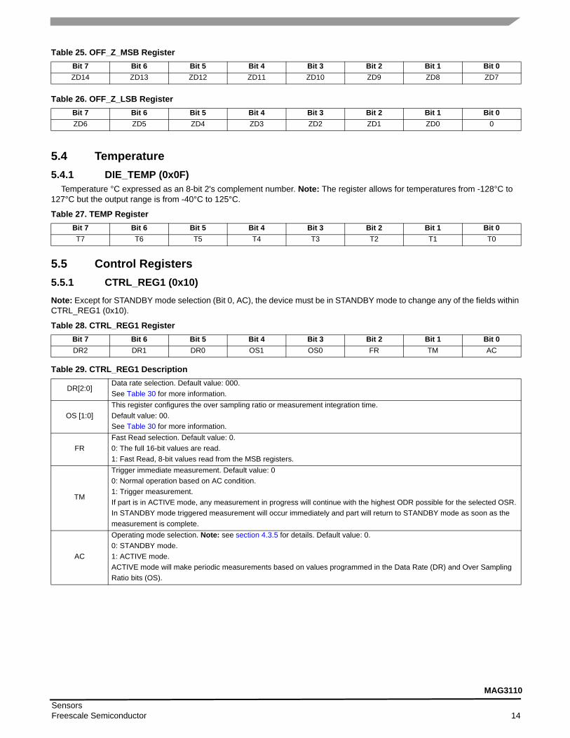
5.4 Temperature 5.4.1 DIE_TEMP (0x0F)
Temperature °C expressed as an 8-bit 2's complement number. Note: The register allows for temperatures from -128°C to 127°C but the output range is from -40°C to 125°C.
5.5 Control Registers5.5.1 CTRL_REG1 (0x10)Note: Except for STANDBY mode selection (Bit 0, AC), the device must be in STANDBY mode to change any of the fields within CTRL_REG1 (0x10).
Table 25. OFF_Z_MSB RegisterBit 7 Bit 6 Bit 5 Bit 4 Bit 3 Bit 2 Bit 1 Bit 0ZD14 ZD13 ZD12 ZD11 ZD10 ZD9 ZD8 ZD7
Table 26. OFF_Z_LSB RegisterBit 7 Bit 6 Bit 5 Bit 4 Bit 3 Bit 2 Bit 1 Bit 0ZD6 ZD5 ZD4 ZD3 ZD2 ZD1 ZD0 0
Table 27. TEMP RegisterBit 7 Bit 6 Bit 5 Bit 4 Bit 3 Bit 2 Bit 1 Bit 0T7 T6 T5 T4 T3 T2 T1 T0
Table 28. CTRL_REG1 RegisterBit 7 Bit 6 Bit 5 Bit 4 Bit 3 Bit 2 Bit 1 Bit 0DR2 DR1 DR0 OS1 OS0 FR TM AC
Table 29. CTRL_REG1 Description
DR[2:0]Data rate selection. Default value: 000.See Table 30 for more information.
OS [1:0]This register configures the over sampling ratio or measurement integration time.Default value: 00.See Table 30 for more information.
FRFast Read selection. Default value: 0.0: The full 16-bit values are read. 1: Fast Read, 8-bit values read from the MSB registers.
TM
Trigger immediate measurement. Default value: 00: Normal operation based on AC condition. 1: Trigger measurement.If part is in ACTIVE mode, any measurement in progress will continue with the highest ODR possible for the selected OSR. In STANDBY mode triggered measurement will occur immediately and part will return to STANDBY mode as soon as the measurement is complete.
AC
Operating mode selection. Note: see section 4.3.5 for details. Default value: 0.0: STANDBY mode. 1: ACTIVE mode.ACTIVE mode will make periodic measurements based on values programmed in the Data Rate (DR) and Over Sampling Ratio bits (OS).
SensorsFreescale Semiconductor 14
MAG3110
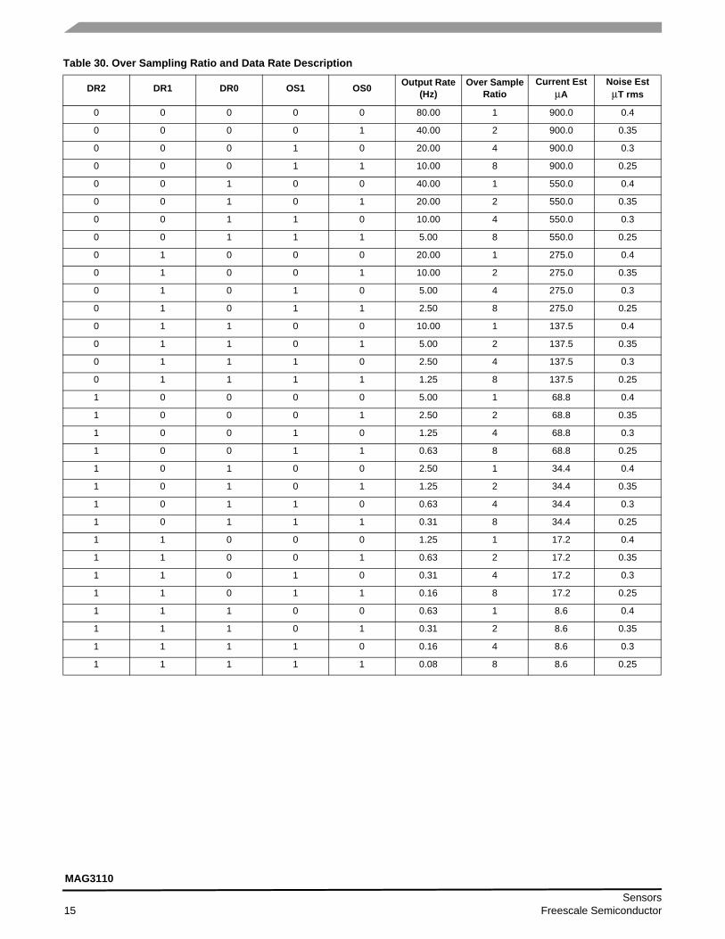
Table 30. Over Sampling Ratio and Data Rate Description
DR2 DR1 DR0 OS1 OS0 Output Rate (Hz)
Over SampleRatio
Current EstμA
Noise EstμT rms
0 0 0 0 0 80.00 1 900.0 0.4
0 0 0 0 1 40.00 2 900.0 0.35
0 0 0 1 0 20.00 4 900.0 0.3
0 0 0 1 1 10.00 8 900.0 0.25
0 0 1 0 0 40.00 1 550.0 0.4
0 0 1 0 1 20.00 2 550.0 0.35
0 0 1 1 0 10.00 4 550.0 0.3
0 0 1 1 1 5.00 8 550.0 0.25
0 1 0 0 0 20.00 1 275.0 0.4
0 1 0 0 1 10.00 2 275.0 0.35
0 1 0 1 0 5.00 4 275.0 0.3
0 1 0 1 1 2.50 8 275.0 0.25
0 1 1 0 0 10.00 1 137.5 0.4
0 1 1 0 1 5.00 2 137.5 0.35
0 1 1 1 0 2.50 4 137.5 0.3
0 1 1 1 1 1.25 8 137.5 0.25
1 0 0 0 0 5.00 1 68.8 0.4
1 0 0 0 1 2.50 2 68.8 0.35
1 0 0 1 0 1.25 4 68.8 0.3
1 0 0 1 1 0.63 8 68.8 0.25
1 0 1 0 0 2.50 1 34.4 0.4
1 0 1 0 1 1.25 2 34.4 0.35
1 0 1 1 0 0.63 4 34.4 0.3
1 0 1 1 1 0.31 8 34.4 0.25
1 1 0 0 0 1.25 1 17.2 0.4
1 1 0 0 1 0.63 2 17.2 0.35
1 1 0 1 0 0.31 4 17.2 0.3
1 1 0 1 1 0.16 8 17.2 0.25
1 1 1 0 0 0.63 1 8.6 0.4
1 1 1 0 1 0.31 2 8.6 0.35
1 1 1 1 0 0.16 4 8.6 0.3
1 1 1 1 1 0.08 8 8.6 0.25
Sensors15 Freescale Semiconductor
MAG3110
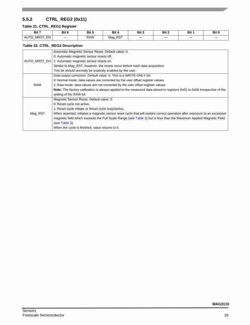
5.5.2 CTRL_REG2 (0x11)Table 31. CTRL_REG2 Register
Bit 7 Bit 6 Bit 5 Bit 4 Bit 3 Bit 2 Bit 1 Bit 0AUTO_MRST_EN — RAW Mag_RST — — — —
Table 32. CTRL_REG2 Description
AUTO_MRST_EN
Automatic Magnetic Sensor Reset. Default value: 0.0: Automatic magnetic sensor resets off.1: Automatic magnetic sensor resets on.Similar to Mag_RST, however, the resets occur before each data acquisition.This bit should normally be explicitly enabled by the user.
RAW
Data output correction. Default value: 0. This is a WRITE-ONLY bit.0: Normal mode: data values are corrected by the user offset register values.1: Raw mode: data values are not corrected by the user offset register values. Note: The factory calibration is always applied to the measured data stored in registers 0x01 to 0x06 irrespective of the setting of the RAW bit.
Mag_RST
Magnetic Sensor Reset. Default value: 0.0: Reset cycle not active. 1: Reset cycle initiate or Reset cycle busy/active.When asserted, initiates a magnetic sensor reset cycle that will restore correct operation after exposure to an excessive magnetic field which exceeds the Full Scale Range (see Table 2) but is less than the Maximum Applied Magnetic Field (see Table 3).When the cycle is finished, value returns to 0.
SensorsFreescale Semiconductor 16
MAG3110

6 Geomagnetic Field MapsThe magnitude of the geomagnetic field varies from 25 μT in South America to about 60 μT over Northern China. The
horizontal component of the field varies from zero at the magnetic poles to 40 μT.These web sites have further information:
http://wdc.kugi.kyoto-u.ac.jp/igrf/
http://geomag.usgs.gov
Sensors17 Freescale Semiconductor
MAG3110
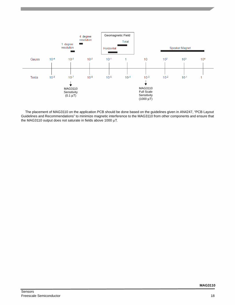
The placement of MAG3110 on the application PCB should be done based on the guidelines given in AN4247, “PCB Layout Guidelines and Recommendations” to minimize magnetic interference to the MAG3110 from other components and ensure that the MAG3110 output does not saturate in fields above 1000 μT.
Geomagnetic Field
MAG3110MAG3110Sensitivity Full Scale
Sensitivity(0.1 μT)(1000 μT)
SensorsFreescale Semiconductor 18
MAG3110
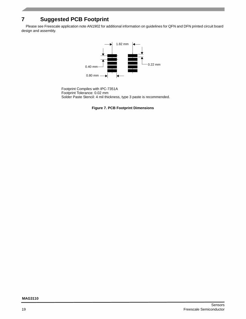
7 Suggested PCB FootprintPlease see Freescale application note AN1902 for additional information on guidelines for QFN and DFN printed circuit board
design and assembly.
Figure 7. PCB Footprint Dimensions
1.82 mm
0.22 mm
0.80 mm
0.40 mm
Footprint Compiles with IPC-7351AFootprint Tolerance: 0.02 mmSolder Paste Stencil: 4 mil thickness, type 3 paste is recommended.
Sensors19 Freescale Semiconductor
MAG3110
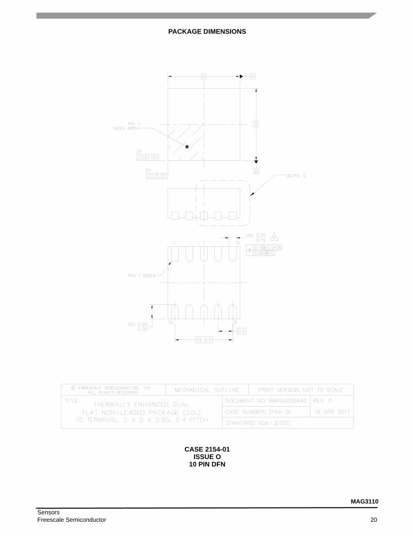
PACKAGE DIMENSIONS
CASE 2154-01ISSUE O
10 PIN DFN
SensorsFreescale Semiconductor 20
MAG3110
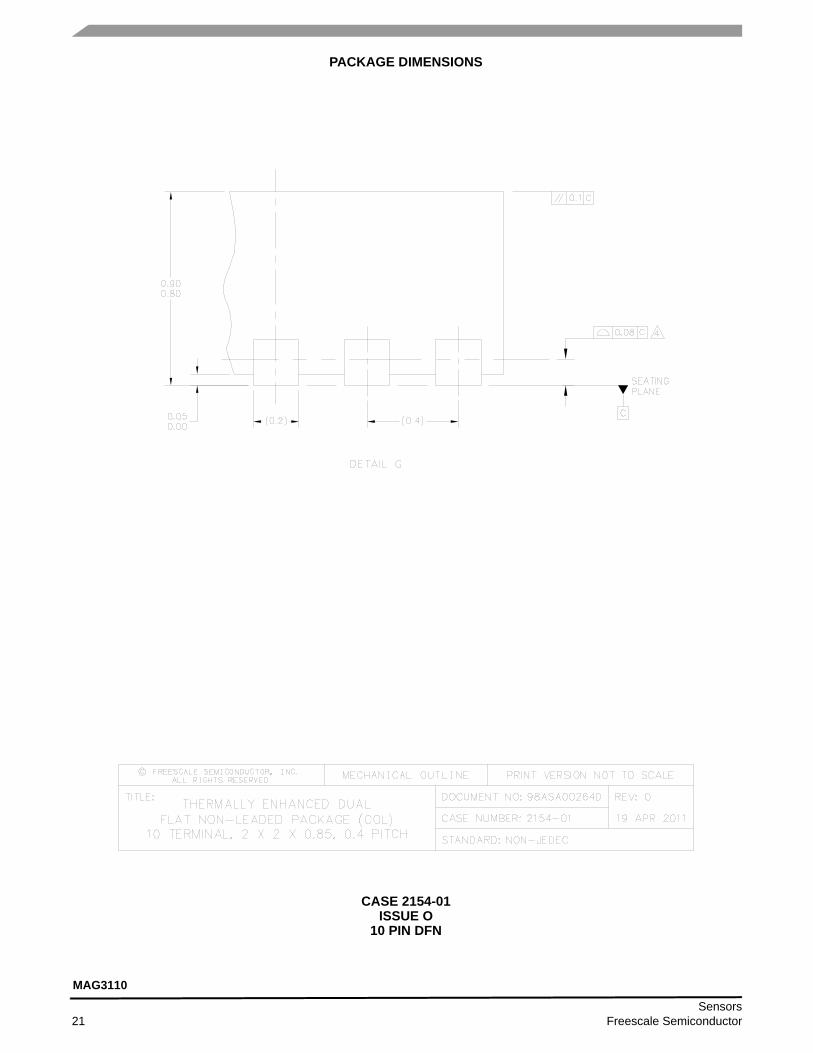
PACKAGE DIMENSIONS
CASE 2154-01ISSUE O
10 PIN DFN
Sensors21 Freescale Semiconductor
MAG3110

PACKAGE DIMENSIONS
CASE 2154-01ISSUE O
10 PIN DFN
SensorsFreescale Semiconductor 22
MAG3110
MAG3110Rev. 505/2011
Information in this document is provided solely to enable system and software implementers to use Freescale Semiconductor products. There are no express or implied copyright licenses granted hereunder to design or fabricate any integrated circuits or integrated circuits based on the information in this document.
Freescale Semiconductor reserves the right to make changes without further notice to any products herein. Freescale Semiconductor makes no warranty, representation or guarantee regarding the suitability of its products for any particular purpose, nor does Freescale Semiconductor assume any liability arising out of the application or use of any product or circuit, and specifically disclaims any and all liability, including without limitation consequential or incidental damages. “Typical” parameters that may be provided in Freescale Semiconductor data sheets and/or specifications can and do vary in different applications and actual performance may vary over time. All operating parameters, including “Typicals”, must be validated for each customer application by customer’s technical experts. Freescale Semiconductor does not convey any license under its patent rights nor the rights of others. Freescale Semiconductor products are not designed, intended, or authorized for use as components in systems intended for surgical implant into the body, or other applications intended to support or sustain life, or for any other application in which the failure of the Freescale Semiconductor product could create a situation where personal injury or death may occur. Should Buyer purchase or use Freescale Semiconductor products for any such unintended or unauthorized application, Buyer shall indemnify and hold Freescale Semiconductor and its officers, employees, subsidiaries, affiliates, and distributors harmless against all claims, costs, damages, and expenses, and reasonable attorney fees arising out of, directly or indirectly, any claim of personal injury or death associated with such unintended or unauthorized use, even if such claim alleges that Freescale Semiconductor was negligent regarding the design or manufacture of the part.
Freescale and the Freescale logo are trademarks of Freescale Semiconductor, Inc., Reg. U.S. Pat. & Tm. Off. Xtrinsic is a trademark of Freescale Semiconductor, Inc.All other product or service names are the property of their respective owners.© Freescale Semiconductor, Inc. 2011. All rights reserved.
RoHS-compliant and/or Pb-free versions of Freescale products have the functionality and electrical characteristics of their non-RoHS-compliant and/or non-Pb-free counterparts. For furtherinformation, see http:/www.freescale.com or contact your Freescale sales representative.
For information on Freescale’s Environmental Products program, go to http://www.freescale.com/epp.
How to Reach Us:
Home Page:www.freescale.com
Web Support:http://www.freescale.com/support
USA/Europe or Locations Not Listed:Freescale Semiconductor, Inc.Technical Information Center, EL5162100 East Elliot RoadTempe, Arizona 852841-800-521-6274 or +1-480-768-2130www.freescale.com/support
Europe, Middle East, and Africa:Freescale Halbleiter Deutschland GmbHTechnical Information CenterSchatzbogen 781829 Muenchen, Germany+44 1296 380 456 (English)+46 8 52200080 (English)+49 89 92103 559 (German)+33 1 69 35 48 48 (French)www.freescale.com/support
Japan:Freescale Semiconductor Japan Ltd.HeadquartersARCO Tower 15F1-8-1, Shimo-Meguro, Meguro-ku,Tokyo 153-0064Japan0120 191014 or +81 3 5437 [email protected]
Asia/Pacific:Freescale Semiconductor China Ltd.Exchange Building 23FNo. 118 Jianguo RoadChaoyang DistrictBeijing 100022 China +86 010 5879 [email protected]
For Literature Requests Only:Freescale Semiconductor Literature Distribution Center1-800-441-2447 or +1-303-675-2140Fax: [email protected]