2010 electronic materials conference ashish baraskar june 23-25, 2010 – notre dame, in 1 in-situ...
Post on 21-Dec-2015
214 views
TRANSCRIPT

2010 Electronic Materials Conference Ashish BaraskarJune 23-25, 2010 – Notre Dame, IN 1
In-situ Ohmic Contacts to p-InGaAs
Ashish Baraskar, Vibhor Jain, Evan Lobisser, Brian Thibeault, Arthur Gossard and Mark Rodwell
ECE and Materials Departments, University of California, Santa Barbara, CA
Mark WisteyElectrical Engineering, University of Notre Dame, IN
2010 Electronic Materials Conference Ashish BaraskarJune 23-25, 2010 – Notre Dame, IN 2
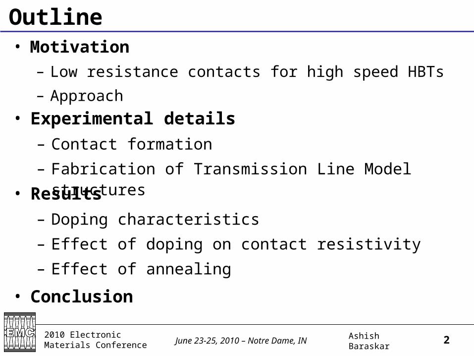
Outline• Motivation
– Low resistance contacts for high speed HBTs
– Approach• Experimental details
– Contact formation
– Fabrication of Transmission Line Model structures
• Results
– Doping characteristics
– Effect of doping on contact resistivity
– Effect of annealing
• Conclusion

2010 Electronic Materials Conference Ashish BaraskarJune 23-25, 2010 – Notre Dame, IN 3
Outline• Motivation
– Low resistance contacts for high speed HBTs
– Approach• Experimental details
– Contact formation
– Fabrication of Transmission Line Model structures
• Results
– Doping characteristics
– Effect of doping on contact resistivity
– Effect of annealing
• Conclusion
2010 Electronic Materials Conference Ashish BaraskarJune 23-25, 2010 – Notre Dame, IN 4
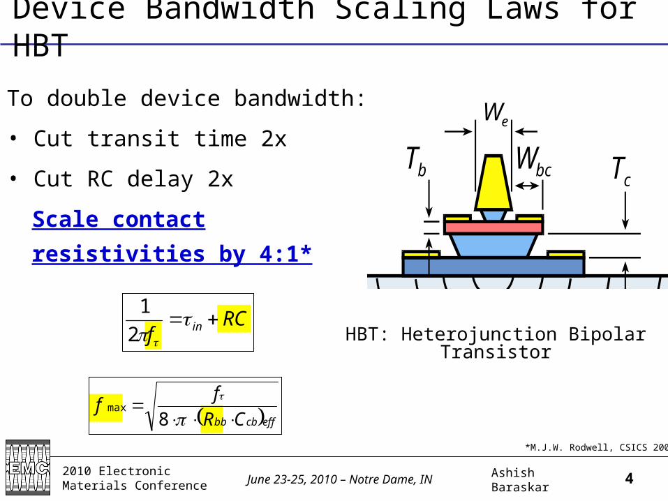
Device Bandwidth Scaling Laws for HBT
To double device bandwidth:
• Cut transit time 2x
• Cut RC delay 2x
Scale contact resistivities by 4:1*
*M.J.W. Rodwell, CSICS 2008
bcWcTbT
eW
HBT: Heterojunction Bipolar TransistorRC
f in 2
1
effcbbb CR
ff
8max
2010 Electronic Materials Conference Ashish BaraskarJune 23-25, 2010 – Notre Dame, IN 5
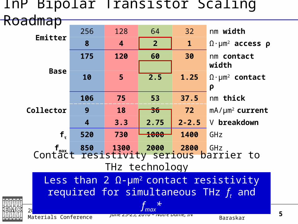
InP Bipolar Transistor Scaling Roadmap
Emitter256 128 64 32 nm width
8 4 2 1 Ω·µm2 access ρ
Base175 120 60 30 nm contact width
10 5 2.5 1.25 Ω·µm2 contact ρ
Collector
106 75 53 37.5 nm thick
9 18 36 72 mA/µm2 current
4 3.3 2.75 2-2.5 V breakdown
fτ 520 730 1000 1400 GHz
fmax 850 1300 2000 2800 GHz
Contact resistivity serious barrier to THz technology
Less than 2 Ω-µm2 contact resistivity required for simultaneous THz ft and fmax*

2010 Electronic Materials Conference Ashish BaraskarJune 23-25, 2010 – Notre Dame, IN 6
Approach
To achieve low resistance, stable ohmic contacts
• Higher number of active carriers
- Reduced depletion width
- Enhanced tunneling across metal-
semiconductor interface
• Better surface preparation techniques
- For efficient removal of oxides/impurities

2010 Electronic Materials Conference Ashish BaraskarJune 23-25, 2010 – Notre Dame, IN 7
• Scaled device thin base
(For 80 nm device: tbase < 25 nm)
• Non-refractory contacts may diffuse at higher temperatures through
base and short the collector• Pd/Ti/Pd/Au contacts diffuse about 15 nm in InGaAs on annealing
Approach (contd.)
100 nm InGaAs grown in MBE
15 nm Pd/Ti diffusion
Need a refractory metal for thermal stability
2010 Electronic Materials Conference Ashish BaraskarJune 23-25, 2010 – Notre Dame, IN 8
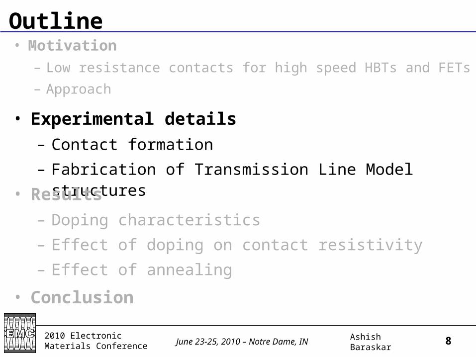
Outline• Motivation
– Low resistance contacts for high speed HBTs and FETs
– Approach• Experimental details
– Contact formation
– Fabrication of Transmission Line Model structures
• Results
– Doping characteristics
– Effect of doping on contact resistivity
– Effect of annealing
• Conclusion

2010 Electronic Materials Conference Ashish BaraskarJune 23-25, 2010 – Notre Dame, IN 9
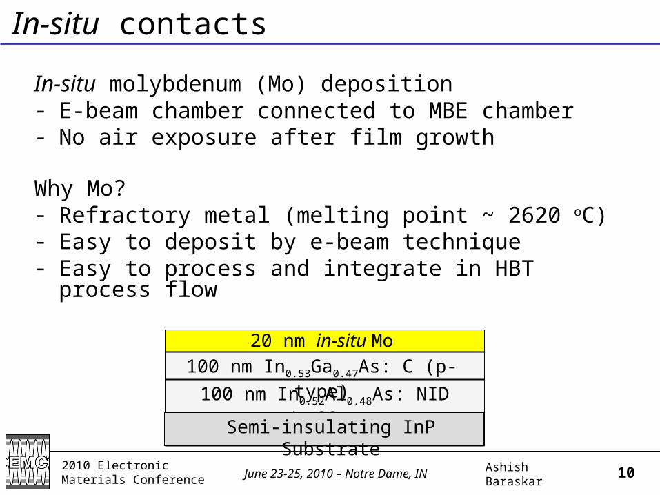
Semi-insulating InP Substrate
100 nm In0.52Al0.48As: NID buffer
100 nm In0.53Ga0.47As: C (p-type)
Epilayer growth by Solid Source Molecular Beam Epitaxy (SS-MBE)– p-InGaAs/InAlAs
- Semi insulating InP (100) substrate
- Un-doped InAlAs buffer
- CBr4 as carbon dopant source
- Hole concentration determined by Hall measurements
Epilayer Growth
2010 Electronic Materials Conference Ashish BaraskarJune 23-25, 2010 – Notre Dame, IN 10
100 nm In0.52Al0.48As: NID buffer
100 nm In0.53Ga0.47As: C (p-type)
20 nm in-situ Mo
Semi-insulating InP Substrate
In-situ contacts
In-situ molybdenum (Mo) deposition - E-beam chamber connected to MBE chamber- No air exposure after film growth
Why Mo? - Refractory metal (melting point ~ 2620 oC)- Easy to deposit by e-beam technique- Easy to process and integrate in HBT process flow

2010 Electronic Materials Conference Ashish BaraskarJune 23-25, 2010 – Notre Dame, IN 11
TLM (Transmission Line Model) fabrication
• E-beam deposition of Ti, Au and Ni layers
• Samples processed into TLM structures by photolithography and liftoff
• Contact metal was dry etched in SF6/Ar with Ni as etch mask, isolated by wet etch
100 nm In0.52Al0.48As: NID buffer
100 nm In0.53Ga0.47As: C (p-type)
20 nm in-situ Mo20 nm ex-situ Ti
50 nm ex-situ Ni500 nm ex-situ Au
Semi-insulating InP Substrate

2010 Electronic Materials Conference Ashish BaraskarJune 23-25, 2010 – Notre Dame, IN 12
• Resistance measured by Agilent 4155C semiconductor parameter
analyzer
• TLM pad spacing (Lgap) varied from 0.5-26 µm; verified from
scanning electron microscope (SEM)
• TLM Width ~ 25 µm
Resistance Measurement
W
RR ShC
C
22
0
1
2
3
4
5
0 0.5 1 1.5 2 2.5 3 3.5
Gap Spacing (m)
Res
ista
nce
()

2010 Electronic Materials Conference Ashish BaraskarJune 23-25, 2010 – Notre Dame, IN 13
• Extrapolation errors:– 4-point probe resistance
measurements on Agilent 4155C
– Resolution error in SEM
0
0.5
1
1.5
2
2.5
3
3.5
0 1 2 3 4 5 6
Res
ista
nce
()
Gap Spacing (m)
R
d
Rc
Error Analysis• Processing errors:
Lgap
W
Variable gap along width (W)
1.10 µm 1.04 µm
– Variable gap spacing along width (W)
Overlap Resistance
– Overlap resistance
2010 Electronic Materials Conference Ashish BaraskarJune 23-25, 2010 – Notre Dame, IN 14
Outline• Motivation
– Low resistance contacts for high speed HBTs and FETs
– Approach• Experimental details
– Contact formation
– Fabrication of Transmission Line Model structures
• Results
– Doping characteristics
– Effect of doping on contact resistivity
– Effect of annealing
• Conclusion
2010 Electronic Materials Conference Ashish BaraskarJune 23-25, 2010 – Notre Dame, IN 15
1019
1020
40
50
60
70
80
0 10 20 30 40 50 60
hole concentration
mobility
Mob
ility
(cm
2 -Vs)
CBr4 foreline pressure (mtorr)
Hol
e C
once
ntra
tion
(cm
-3)
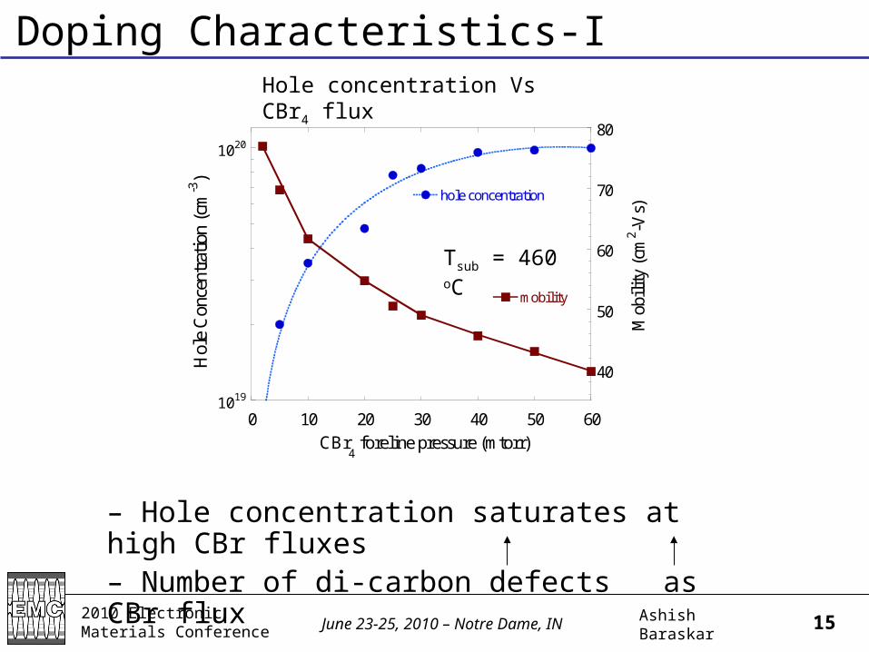
Doping Characteristics-IHole concentration Vs CBr4 flux
– Hole concentration saturates at high CBr fluxes– Number of di-carbon defects as CBr flux
Tsub = 460 oC
2010 Electronic Materials Conference Ashish BaraskarJune 23-25, 2010 – Notre Dame, IN 16
2
4
6
8
10
10 20 30 40 50 60
Group V / Group III
Hol
e C
once
ntra
tion
(10
19)
cm-3
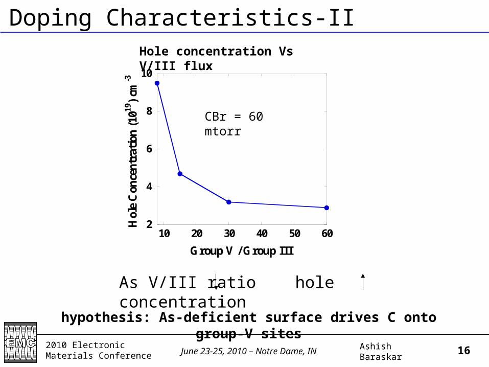
As V/III ratio hole concentration
hypothesis: As-deficient surface drives C onto group-V sites
Doping Characteristics-IIHole concentration Vs V/III flux
CBr = 60 mtorr
2010 Electronic Materials Conference Ashish BaraskarJune 23-25, 2010 – Notre Dame, IN 17
4 1019
8 1019
1.2 1020
1.6 1020
2 1020
300 350 400 450
Hol
e C
once
ntra
tion
(cm
-3)
Substrate Temp. (oC)
CBr = 60 mtorr
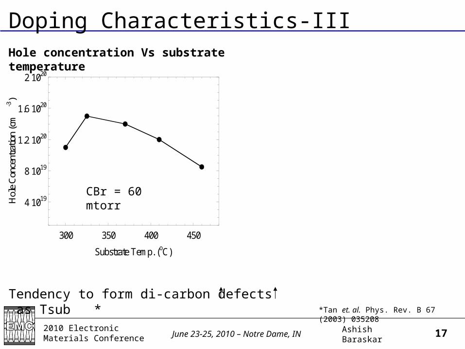
Doping Characteristics-IIIHole concentration Vs substrate temperature
*Tan et. al. Phys. Rev. B 67 (2003) 035208
Tendency to form di-carbon defects as Tsub *

2010 Electronic Materials Conference Ashish BaraskarJune 23-25, 2010 – Notre Dame, IN 18
4 1019
8 1019
1.2 1020
1.6 1020
2 1020
300 350 400 450
Hol
e C
once
ntra
tion
(cm
-3)
Substrate Temp. (oC)
CBr = 60 mtorr
Doping Characteristics-IIIHole concentration Vs substrate temperature
*Tan et. al. Phys. Rev. B 67 (2003) 035208
1019
1020
0 20 40 60 80 100
Tsub = 460 oC
Tsub = 350 oC
CBr4 foreline pressure (mtorr)
Hol
e C
once
ntra
tion
(cm
-3)
Tendency to form di-carbon defects as Tsub *

2010 Electronic Materials Conference Ashish BaraskarJune 23-25, 2010 – Notre Dame, IN 19
ρc lower than the best reported contacts to
pInGaAs (ρc = 4 Ω-µm2)[1,2]0
5
10
15
20
0 1 2 3 4
Re
sist
an
ce (
)Gap Spacing (m)
1. Griffith et al, Indium Phosphide and Related Materials, 2005.
2. Jain et al, IEEE Device Research Conference, 2010.
W
RR ShC
C
22
• Hole concentration, p = 1.6 x 1020 cm-3
• Mobility, µ = 36 cm2/Vs• Sheet resistance, Rsh = 105 ohm/ (100 nm thick film)
Results: Contact Resistivity - I
Metal Contact ρc (Ω-µm2) ρh (Ω-µm)
In-situ Mo 2.2 ± 0.8 15.4 ± 2.6

2010 Electronic Materials Conference Ashish BaraskarJune 23-25, 2010 – Notre Dame, IN 20
1
10
5 10 15
Con
tact
Res
istiv
ity, c (
-
m2 )
[p]-1/2 (x10-11 cm-3/2)
*
1exp
pCTunneling
Data suggests tunneling
ThermionicEmission c ~ constant*
High active carrier concentration is the key to low resistance contacts
* Physics of Semiconductor Devices, S M Sze
Results: Contact Resistivity - II

2010 Electronic Materials Conference Ashish BaraskarJune 23-25, 2010 – Notre Dame, IN 21
Mo contacts annealed under N2 flow for 60 mins. at 250 oC
Thermal Stability - I
• ρc increases on annealing
• Mo reacts with residual
interfacial carbon?*
*Kiniger et. al., Surf. Interface Anal. 2008, 40, 786–789
Kiniger et. al.*
Molybdenum C substrate
Before annealing After annealing
ρc (Ω-µm2) 2.2 ± 0.8 2.8 ± 0.9

2010 Electronic Materials Conference Ashish BaraskarJune 23-25, 2010 – Notre Dame, IN 22
Mo contacts annealed under N2 flow for 60 mins. at 250 oC
TEM of Mo-pInGaAs interface
- Suggests sharp interface
- Minimal/No intermixing
200 nm InAlAs
InGaAsMo
Ti
Au
Thermal Stability - II
2010 Electronic Materials Conference Ashish BaraskarJune 23-25, 2010 – Notre Dame, IN 23
Summary
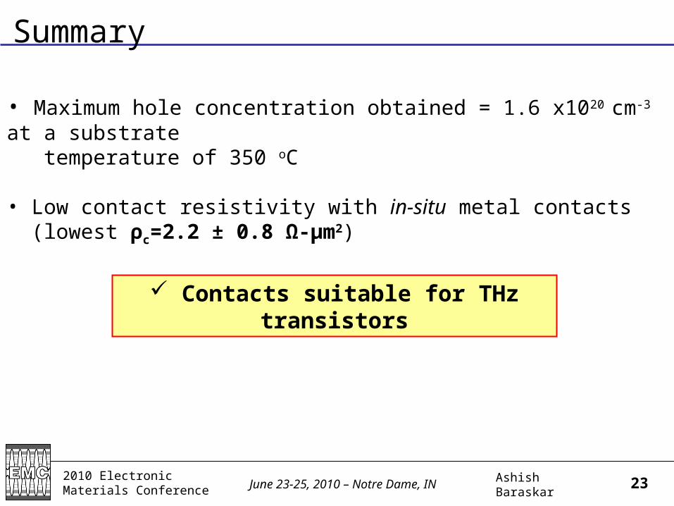
• Maximum hole concentration obtained = 1.6 x1020 cm-3 at a substrate temperature of 350 oC
• Low contact resistivity with in-situ metal contacts (lowest ρc=2.2 ± 0.8 Ω-µm2)
Contacts suitable for THz transistors

2010 Electronic Materials Conference Ashish BaraskarJune 23-25, 2010 – Notre Dame, IN 24
Thank You !
Questions?
Acknowledgements
ONR, DARPA-TFAST, DARPA-FLARE
2010 Electronic Materials Conference Ashish BaraskarJune 23-25, 2010 – Notre Dame, IN 25
Extra Slides
2010 Electronic Materials Conference Ashish BaraskarJune 23-25, 2010 – Notre Dame, IN 26
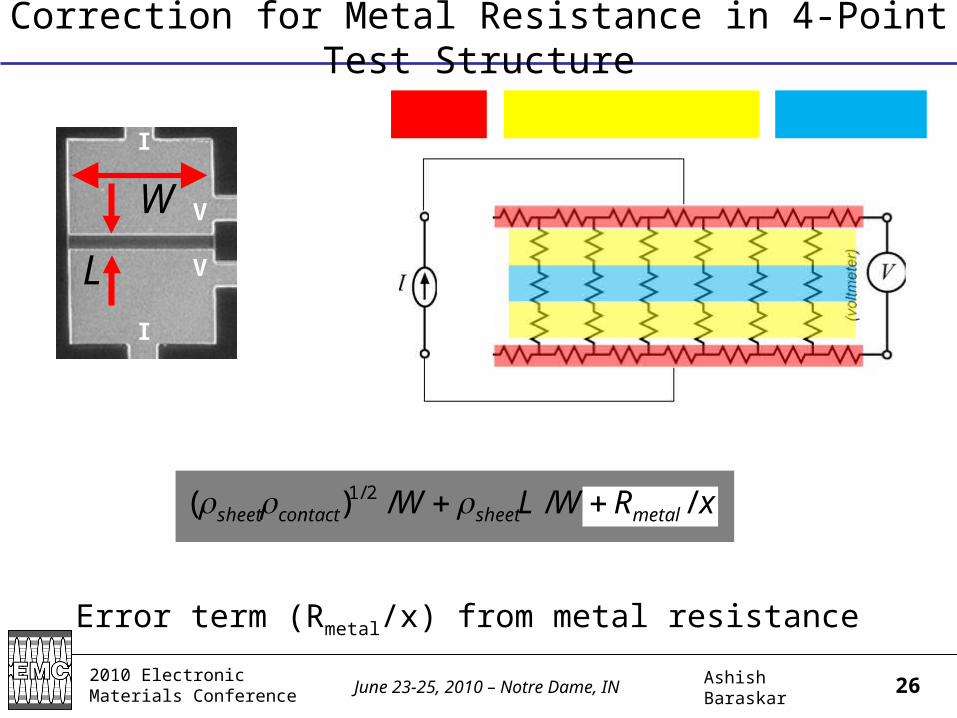
Correction for Metal Resistance in 4-Point Test Structure
WLsheet /metalR Wcontactsheet /)( 2/1
Error term (Rmetal/x) from metal resistance
L
W
I
I
V
V
xRWLW metalsheetcontactsheet ///)( 2/1

2010 Electronic Materials Conference Ashish BaraskarJune 23-25, 2010 – Notre Dame, IN 27
Random and Offset Error in 4155C
0.6642
0.6643
0.6644
0.6645
0.6646
0.6647
0 5 10 15 20 25
Res
ista
nce
(
)
Current (mA)
• Random Error in resistance measurement ~ 0.5 m
• Offset Error < 5 m*
*4155C datasheet

2010 Electronic Materials Conference Ashish BaraskarJune 23-25, 2010 – Notre Dame, IN 28
Accuracy Limits
• Error Calculations– dR = 50 mΩ (Safe estimate)– dW = 1 µm– dGap = 20 nm
• Error in ρc ~ 40% at 1.1 Ω-µm2