18-bit, 15 msps, µmodule data acquisition solution
TRANSCRIPT

Data SheetADAQ23878
18-Bit, 15 MSPS, µModule Data Acquisition Solution
Rev. 0DOCUMENT FEEDBACK
TECHNICAL SUPPORT
Information furnished by Analog Devices is believed to be accurate and reliable "as is". However, no responsibility is assumed by AnalogDevices for its use, nor for any infringements of patents or other rights of third parties that may result from its use. Specifications subject tochange without notice. No license is granted by implication or otherwise under any patent or patent rights of Analog Devices. Trademarks andregistered trademarks are the property of their respective owners.
FEATURES
Integrated fully differential ADC driver with signal scaling Wide input common-mode voltage range High common-mode rejection
Single-ended to differential conversion Pin selectable input range with overrange
Input ranges with 4.096 V REFBUF: ±10 V, ±5 V, ±4.096 V,±2.5 V, and ±1.5 V
Gain/attenuation options: 0.37, 0.73, 0.87, 1.38, and 2.25 Critical passive components 0.005% precision matched resistor array for FDA
9 mm × 9 mm, 0.8 mm pitch, 100-ball CSP_BGA package 2.5× footprint reduction vs. discrete solution
Low power, dynamic power scaling, power-down mode 143 mW typical at 15 MSPS
Throughput: 15 MSPS, no pipeline delay INL error: ±3.1 ppm typical, ±6.2 ppm maximum
(Gain = 0.73, gain = 0.87, gain = 1.38, gain = 2.25) SINAD: 90.4 dB typical at 20 kHz (gain = 0.73) THD: −117 dB at 1 kHz, −110 dB at 100 kHz (gain = 0.73) Gain error: ±0.005%FS typical Gain error drift: ±0.13 ppm/°C typical On-board reference buffer with VCMO generation Serial LVDS interface Wide operating temperature range: −40°C to +85°C
APPLICATIONS
Automatic test equipment Data acquisition Hardware in the Loop (HiL) Power analyzers Nondestructive test (acoustic emissions)
Mass spectrometry Traveling wave fault location Medical imaging and instruments
GENERAL DESCRIPTION
The ADAQ23878 is a precision, high speed, μModule® data acquis-ition solution that reduces the development cycle of precision meas-urement systems by transferring the design burden of componentselection, optimization, and layout from the designer to the device.Using system-in-package (SIP) technology, the ADAQ23878 re-duces end system component count by combining multiple commonsignal processing and conditioning blocks in a single device, includ-ing a low noise, fully differential ADC driver amplifier (FDA), a stablereference buffer, and a high speed, 18-bit, 15 MSPS successiveapproximation register (SAR) ADC.The ADAQ23878 also incorporates the critical passive componentswith superior matching and drift characteristics using Analog Devi-ces, Inc., iPassive® technology to minimize temperature dependenterror sources and to offer optimized performance. The fast settlingof the ADC driver stage and no latency of the SAR ADC providea unique solution for high channel count, multiplexed signal chainarchitectures and control loop applications.The small footprint, 9 mm × 9 mm, 0.8 mm pitch, 100-ballCSP_BGA package enables smaller form factor instruments with-out sacrificing performance. The system integration solves manydesign challenges while the device still provides the flexibility of aconfigurable ADC driver feedback loop to allow gain or attenuationadjustments, as well as fully differential or single-ended to differen-tial input. A single 5 V supply operation is possible while achievingoptimum performance from the device.The ADAQ23878 features a serial low voltage differential signaling(LVDS) digital interface with one-lane or two-lane output modes,allowing the user to optimize the interface data rate for each appli-cation. The specified operation of the ADAQ23878 is from −40°C to+85°C.
FUNCTIONAL BLOCK DIAGRAM
Figure 1. ADAQ23878 Configured for Gain = 0.37, ±10 V Differential Input Range
Data Sheet ADAQ23878TABLE OF CONTENTS
analog.com Rev. 0 | 2 of 37
Features................................................................ 1Applications........................................................... 1General Description...............................................1Functional Block Diagram......................................1Specifications........................................................ 3
Timing Specifications......................................... 7Absolute Maximum Ratings...................................9
Thermal Resistance........................................... 9Electrostatic Discharge (ESD) Ratings...............9ESD Caution.......................................................9
Pin Configuration and Function Descriptions...... 10Typical Performance Characteristics................... 12Terminology......................................................... 23Theory of Operation.............................................25
Circuit Information ........................................... 25
Transfer Function ............................................ 25Applications Information...................................... 26
Typical Application Diagrams .......................... 26Voltage Reference Input...................................30Common-Mode Output.....................................30Power Supply................................................... 30
Digital Interface....................................................32One-Lane Output Mode ...................................32Two-Lane Output Mode ...................................32Output Test Patterns ........................................35
Board Layout ...................................................... 36Mechanical Stress Shift ...................................36
Outline Dimensions ............................................ 37Ordering Guide.................................................37Evaluation Boards............................................ 37
REVISION HISTORY
12/2021—Revision 0: Initial Version

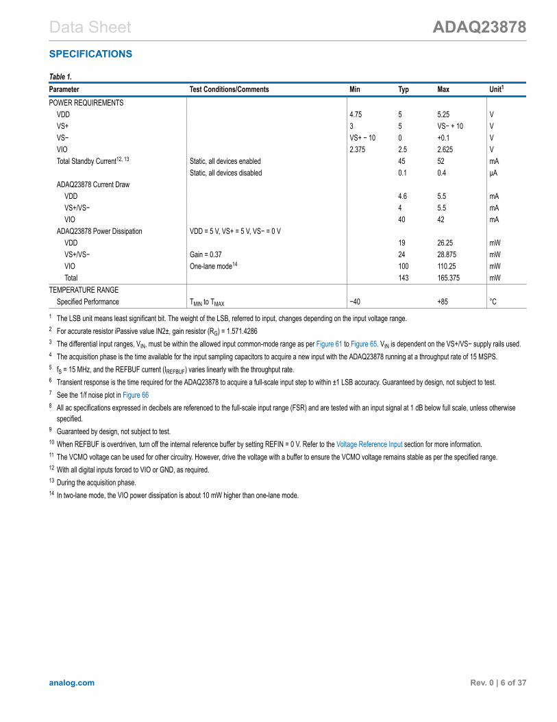
Data Sheet ADAQ23878SPECIFICATIONS
analog.com Rev. 0 | 3 of 37
VDD = 5 V ± 5%, VS+ = 5 V ± 5%, VS− = −1 V ± 5%, VS− = 0 V (95% of VIN), VIO = 2.375 V to 2.625 V, REFBUF = 4.096 V, samplingfrequency (fS) = 15 MSPS, gain = 0.37, 0.73, 0.87, 1.38, and 2.25, and all specifications TMIN to TMAX, unless otherwise noted. For all gainvalues, limit the differential input range, VIN, to 95% to allow enough footroom for the ADC driver with VS− = 0 V to achieve the specifiedperformance.
Table 1.Parameter Test Conditions/Comments Min Typ Max Unit1
RESOLUTION 18 BitsANALOG INPUT IMPEDANCE, ZIN IN1+, IN1−, IN2+, IN2−, SJ+, and SJ− single-ended to
differential configurationGain = 0.37 (resistor feedback (RF) = 1375 Ω || 1000 Ω),VIN = 20 V p-p
1816 Ω
Gain = 0.73 (RF = 1571 Ω2 || 1375 Ω), VIN = 10 V p-p 1268 ΩGain = 0.87, VIN = 8.1912 V p-p 2050 ΩGain = 1.38, VIN = 5 V p-p 1407 ΩGain = 2.25 (RF = 1571 Ω || 1000 Ω), VIN = 3 V p-p 935 ΩFully differential configurationGain = 0.37 (RF = 1375 Ω || 1000 Ω), VIN = 20 V p-p 3143 ΩGain = 0.73 (RF = 1571 Ω || 1375 Ω), VIN = 10 V p-p 2000 ΩGain = 0.87, VIN = 8.1912 V p-p 3143 ΩGain = 1.38, VIN = 5 V p-p 2000 ΩGain = 2.25 (RF = 1571 Ω || 1000 Ω), VIN = 3 V p-p 1222 Ω
Input Capacitance IN1+, IN1− 3.3 pFDifferential Input Voltage Range, VIN
3 Gain = 0.37, VIN = 22.141 V p-p −11 +11 VGain = 0.73, VIN = 11.222 V p-p −5.6 +5.6 VGain = 0.87, VIN = 9.416 V p-p −4.7 +4.7 VGain = 1.38, VIN = 5.936 V p-p −2.9 +2.9 VGain = 2.25, VIN = 3.64 V p-p −1.8 +1.8 V
THROUGHPUTComplete Cycle 66.6 nsConversion Time 54 58 63 nsAcquisition Phase4 Time
betweenconversions(tCYC) − 39
ns
Throughput Rate5 0.02 15 MSPSTransient Response6 Full-scale step 52 ns
DC ACCURACY Single-ended and differential configurationNo Missing Codes 18 BitsIntegral Nonlinearity (INL) Error
Gain = 0.37 single-ended −7.5 −7, +1.5 +2.5 LSB−23.4 −21.8, +4.6 +7.8 ppm
Gain = 0.37 differential −2.5 ±1.5 +2.5 LSB−7.8 ±4.6 +7.8 ppm
Gain = 0.73, gain = 0.87, gain = 1.38, and gain = 2.25 −2.0 ±1.0 +2.0 LSB−6.2 ±3.1 +6.2 ppm
Differential Nonlinearity (DNL) Error All gains −0.9 ±0.5 +0.9 LSBTransition Noise 0.73 LSBRMSGain Error All gains −0.025 ±0.005 +0.025 %FSGain Error Drift −0.36 ±0.13 +0.36 ppm/°COffset Error −2.1 +2.1 mVOffset Error Drift −12 ±2.2 +12 ppm/°C

Data Sheet ADAQ23878SPECIFICATIONS
analog.com Rev. 0 | 4 of 37
Table 1.Parameter Test Conditions/Comments Min Typ Max Unit1
Common-Mode Rejection Ratio (CMRR),Input Referred
∆VICM/∆VOSDIFF
All gains 100 dBPower Supply Rejection Ratio (PSRR)
Positive VDD = 4.75 V to 5.25 VAll gains 107 dB
Negative VS+ = +5 V, VS− = −0.75 V to −1.25 VAll gains 105 dB
1/f Noise7 Bandwidth = 0.1 Hz to 10 Hz 9 µV p-pInput Current Noise f = 100 kHz 1 pA/√Hz
AC ACCURACY8 Single-ended and differential configurationDynamic Range Input frequency (fIN) = 1 kHz, −60 dB input 89.5 91.5 dBTotal RMS Noise, Referenced to Input (RTI) All gains 91.6 µVRMSInput Voltage Noise All gains 11.28 nV/√HzSignal-to-Noise Ratio (SNR) fIN = 1 kHz, −1 dBFS 85.5 dB
Gain = 0.37 and gain = 0.73 91 dBGain = 0.87, gain = 1.38, and gain = 2.25 90 dBfIN = 100 kHzGain = 0.37 and gain = 0.73 90.5 dBGain = 0.87, gain = 1.38, and gain = 2.25 89.5 dBfIN = 1MHzGain = 0.73 83.2 dBGain = 0.87, gain = 1.38, and gain = 2.25 80 dB
Signal-to-Noise-and-Distortion (SINAD) fIN = 1 kHz 85.4 dBGain = 0.37 and gain = 0.87 90.4 dBGain = 1.38 and gain = 2.25 88.7 dBfIN = 100 kHzGain = 0.37 and gain = 0.73 89.3 dBGain = 0.87 and gain = 1.38 88.4 dBGain = 2.25 87.7 dBfIN = 1MHzGain = 0.73 67.7 dBGain = 0.87 65.6 dBGain = 1.38 63.8 dBGain = 2.25 61.7 dB
Total Harmonic Distortion (THD) fIN = 1 kHzGain = 0.37 −109.9 dBGain = 0.73, gain = 0.87, and gain = 1.38 −117 dBGain = 2.25 −114.3 dBfIN = 100 kHzGain = 0.37 −107.8 dBGain = 0.73 and gain = 2.25 −110 dBGain = 0.87 and gain = 1.38 −111.4 dBfIN = 1MHzGain = 0.73 −67.9 dBGain = 0.87 −65.8 dBGain = 1.38 −63.9 dBGain = 2.25 −61.8 dB

Data Sheet ADAQ23878SPECIFICATIONS
analog.com Rev. 0 | 5 of 37
Table 1.Parameter Test Conditions/Comments Min Typ Max Unit1
Spurious-Free Dynamic Range (SFDR) fIN = 1 kHzGain = 0.37 and gain = 0.87 110.1 dBGain = 0.73, gain = 1.38 and gain = 2.25 117.5 dBfIN = 100 kHzGain = 0.37 and gain = 0.87 104.1 dBGain = 0.73, gain = 1.38, and gain = 2.25 105.8 dBfIN = 1MHzGain = 0.73 68.7 dBGain = 0.87 66.5 dBGain = 1.38 64.6 dBGain = 2.25 62.5 dB
−3 dB Input Bandwidth, RC Filter Output voltage (VOUT) differential (VOUTDIFF) = 2 V p-p 42 MHzAperture Delay9 0 nsAperture Jitter10 0.25 psRMS
REFERENCEREFIN, Internal Reference Output Voltage Output current (IOUT) = 0 μA 2.028 2.048 2.068 V
Temperature Coefficient ±5 ±20 ppm/°COutput Impedance 15 kΩLine Regulation VDD = 4.75 V to 5.25 V 0.3 mV/VInput Voltage Range REFIN overdriven 2.028 2.048 2.068 V
Reference Buffer Output Voltage, REFBUF REFIN = 2.048 V 4.056 4.096 4.136 VInput Voltage Range REFBUF overdriven10 4.056 4.096 4.136 VLoad Current REFBUF = 4.096 V (REFBUF overdriven) 1.75 1.95 mA
REFBUF = 4.096 V (REFBUF overdriven) 0.5 mAVCMO11
Common-Mode Output Voltage REFBUF = 4.096 V, IOUT = 0 μA 2.028 2.048 2.028 VOutput Impedance –1 mA < IOUT < +1 mA 15 Ω
DIGITAL INPUTSLogic Levels
Input Low Voltage, VIL VIO = 2.5 V 0.6 VInput High Voltage, VIH VIO = 2.5 V 1.7 V
Digital Input Current VIN = 0 V to 2.5 V −10 +10 µAInput Pin Capacitance 3 pF
CNV+/CNV– and CLK+/CLK– (LVDS ClockInput)
Differential Input Voltage, VID 175 350 650 mVCommon-Mode Input Voltage, VICM 0.8 1.25 1.7 V
DCO+/DCO–, DA+/DA–, DB+/DB– (LVDSOutputs)
Differential Output Voltage, VOD 100 Ω differential load 247 350 454 mVCommon-Mode Output Voltage, VOS 100 Ω differential load 1.125 1.25 1.375 V
POWER-DOWN MODEADC Driver (PDB_AMP)/ADC (PDB_ADC)
Low Power-down mode <1 VHigh Enabled, normal operation >1.7 V
Data Sheet ADAQ23878SPECIFICATIONS
analog.com Rev. 0 | 6 of 37
Table 1.Parameter Test Conditions/Comments Min Typ Max Unit1
POWER REQUIREMENTSVDD 4.75 5 5.25 VVS+ 3 5 VS− + 10 VVS− VS+ − 10 0 +0.1 VVIO 2.375 2.5 2.625 VTotal Standby Current12, 13 Static, all devices enabled 45 52 mA
Static, all devices disabled 0.1 0.4 µAADAQ23878 Current Draw
VDD 4.6 5.5 mAVS+/VS− 4 5.5 mAVIO 40 42 mA
ADAQ23878 Power Dissipation VDD = 5 V, VS+ = 5 V, VS− = 0 VVDD 19 26.25 mWVS+/VS− Gain = 0.37 24 28.875 mWVIO One-lane mode14 100 110.25 mWTotal 143 165.375 mW
TEMPERATURE RANGESpecified Performance TMIN to TMAX −40 +85 °C
1 The LSB unit means least significant bit. The weight of the LSB, referred to input, changes depending on the input voltage range.2 For accurate resistor iPassive value IN2±, gain resistor (RG) = 1.571.42863 The differential input ranges, VIN, must be within the allowed input common-mode range as per Figure 61 to Figure 65. VIN is dependent on the VS+/VS− supply rails used.4 The acquisition phase is the time available for the input sampling capacitors to acquire a new input with the ADAQ23878 running at a throughput rate of 15 MSPS.5 fS = 15 MHz, and the REFBUF current (IREFBUF) varies linearly with the throughput rate.6 Transient response is the time required for the ADAQ23878 to acquire a full-scale input step to within ±1 LSB accuracy. Guaranteed by design, not subject to test.7 See the 1/f noise plot in Figure 668 All ac specifications expressed in decibels are referenced to the full-scale input range (FSR) and are tested with an input signal at 1 dB below full scale, unless otherwise
specified.9 Guaranteed by design, not subject to test.10 When REFBUF is overdriven, turn off the internal reference buffer by setting REFIN = 0 V. Refer to the Voltage Reference Input section for more information.11 The VCMO voltage can be used for other circuitry. However, drive the voltage with a buffer to ensure the VCMO voltage remains stable as per the specified range.12 With all digital inputs forced to VIO or GND, as required.13 During the acquisition phase.14 In two-lane mode, the VIO power dissipation is about 10 mW higher than one-lane mode.

Data Sheet ADAQ23878SPECIFICATIONS
analog.com Rev. 0 | 7 of 37
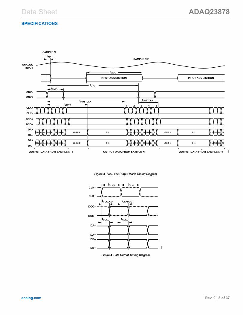
TIMING SPECIFICATIONSVDD = 5 V ± 5%, VS+ = 5 V ± 5%, VS− = −1 V ± 5%, VS− = 0 V (95% of VIN), VIO = 2.375 V to 2.625 V, REFBUF = 4.096 V, samplingfrequency (fS) = 15 MSPS, gain = 0.37, 0.73, 0.87, 1.38, and 2.25, and all specifications TMIN to TMAX, unless otherwise noted.
Table 2. Digital Interface TimingParameter Symbol Min Typ Max UnitSampling Frequency fSMPL 0.02 15 MSPSConversion Time—CNV± Rising Edge to Data Available tCONV 54 58 63 nsAcquisition Phase tACQ tCYC − 39 nsTime Between Conversions tCYC 66.6 50,000 nsCNV± High Time tCNVH 5 nsCNV± Low Time tCNVL 8 nsCNV± Rising Edge to First CLK± Rising Edge from the Same Conversion tFIRSTCLK 65 nsCNV± Rising Edge to Last CLK± Falling Edge from the Previous Conversion tLASTCLK 49 nsCLK± to DCO± Delay tCLKDCO 0.7 1.3 2.3 nsCLK± Low Time tCLKL 1.25 nsCLK± High Time tCLKH 1.25 nsCLK± to DA±/DB± Delay tCLKD 0.7 1.3 2.3 nsDCO± to DA±/DB± Skew tSKEW −200 0 +200 psSampling Delay Time tAP 0 nsSampling Delay Jitter tJITTER 0.25 psRMS
Timing Diagrams
Figure 2. One-Lane Output Mode Timing Diagram
Data Sheet ADAQ23878SPECIFICATIONS
analog.com Rev. 0 | 8 of 37
Figure 3. Two-Lane Output Mode Timing Diagram
Figure 4. Data Output Timing Diagram

Data Sheet ADAQ23878ABSOLUTE MAXIMUM RATINGS
analog.com Rev. 0 | 9 of 37
Table 3.Parameter RatingAnalog Inputs
IN1+, IN1− to GND −12 V to +12 V or 8 mAIN2+, IN2− to GND −12 V to +12 V or 12 mA
Supply VoltageVDD to GND 6 VVIO to GND 2.8 VVS+ to VS− 11 VVS+ to GND −0.3 V to +11 VVS− to GND −11 V to +0.3 VREFBUF to GND −0.3 V to VDD + 0.3 VREFIN to GND −0.3 V to +2.8 V
Digital Inputs to GND −0.3 V to VIO + 0.3 VStorage Temperature Range −65°C to +150°CJunction Temperature 150°CLead Temperature Soldering 260°C reflow as per JEDEC J-
STD-020
Stresses at or above those listed under Absolute Maximum Ratingsmay cause permanent damage to the product. This is a stressrating only; functional operation of the product at these or any otherconditions above those indicated in the operational section of thisspecification is not implied. Operation beyond the maximum operat-ing conditions for extended periods may affect product reliability.
THERMAL RESISTANCEThermal performance is directly linked to printed circuit board(PCB) design and operating environment. Careful attention to PCBthermal design is required.Table 4. Thermal ResistancePackageType1 θJA ΨJT ΨJB
θJCBOTTOM θJC TOP θJB Unit
BC-100-7 48.43 4.64 27.89 9.9 35.15 33.24 °C/W1 Test Condition 1: thermal impedance simulated values are based on use of a
2S2P with vias JEDEC PCB excluding the θJC TOP which uses 1S0P JEDECPCB.
ELECTROSTATIC DISCHARGE (ESD) RATINGSThe following ESD information is provided for the handling of ESDsensitive devices in an ESD protected area only.The human body model (HBM) is per ANSI/ESDA/JEDDEC JS-001.The field induced charged device model (FICDM) per ANSI/ES-DA/JEDEC JS-002.
ESD Ratings for ADAQ23878Table 5. ADAQ23878, 100-Ball CSP_BGAESD Model Withstand Threshold (V)HBM 2250FICDM 1000
ESD CAUTIONESD (electrostatic discharge) sensitive device. Charged devi-ces and circuit boards can discharge without detection. Althoughthis product features patented or proprietary protection circuitry,damage may occur on devices subjected to high energy ESD.Therefore, proper ESD precautions should be taken to avoid
performance degradation or loss of functionality.

Data Sheet ADAQ23878PIN CONFIGURATION AND FUNCTION DESCRIPTIONS
analog.com Rev. 0 | 10 of 37
Figure 5. 100-Ball CSP_BGA Pin Configuration, Top View
Table 6. Pin Function DescriptionsPin No. Mnemonic Type1 DescriptionA1, A7, A9, B7, B9, C6, C7, C8, C9,C10, D2, D4, D5, D7, D8, D9, E1, E2,E3, E5, E6, E7, E8, E9, F3, F4, F5, F6,F7, F8, F9, F10, G1, G2, G3, G4, G5,G6, G7, G8, G9, H2, H3, H4, H5, H6,H7, H8, H9, J2, J5, J6, J7, J8, J9, K1,K2, K4
GND P Power Supply Ground.
A2, B2 IN1− AI Negative Input of the FDA Connected to 1000 Ω Resistor.A3, B3 IN1+ AI Positive Input of the FDA Connected to 1000 Ω Resistor.A4, B4 IN2− AI Negative Input of the FDA Connected to 1571 Ω Resistor.A5, B5 IN2+ AI Positive Input of the FDA Connected to 1571 Ω Resistor.A6 SJ− AI Negative Input of the FDA.B6 SJ+ AI Positive Input of the FDA.A8 VIO P 2.5 V Analog and Output Power Supply. The range of VIO is 2.375 V to 2.625 V. Bypass this pin to
GND with an at least 2.2 μF (0402, X5R) ceramic capacitor.A10 CNV+ DI Conversion Start LVDS Input. A rising edge on CNV+ puts the internal sample-and-hold in hold mode
and starts a conversion cycle. CNV+ can be also driven with a 2.5 V CMOS signal if CNV− isconnected to GND.
B1 PDB_AMP DI Active Low. Connect this pin to GND to power down the fully differential ADC driver. Otherwise,connect this pin to VS+.
B8 TWOLANES DI Digital Input that Enables Two-Lane Output Mode. When TWOLANES is connected high (two-laneoutput mode), the ADAQ23878 outputs two bits at a time on DA−/DA+ and DB−/DB+. WhenTWOLANES is low (one-lane output mode), the ADAQ23878 outputs one bit at a time on DA−/DA+,and DB−/DB+ are disabled. Logic levels are determined by VIO.

Data Sheet ADAQ23878PIN CONFIGURATION AND FUNCTION DESCRIPTIONS
analog.com Rev. 0 | 11 of 37
Table 6. Pin Function DescriptionsPin No. Mnemonic Type1 DescriptionB10 CNV− DI Conversion Start LVDS Input. A rising edge on CNV+ puts the internal sample-and-hold in hold mode
and starts a conversion cycle. CNV+ can be also driven with a 2.5 V CMOS signal if CNV− isconnected to GND.
C1, D1 OUT+ AO Positive Output of the FDA.C2, C4, E4, H1 VS+ P FDA and Reference Buffer Positive Supply. The LDO output generating the VS+ supply of µModule
must be bypassed with at least 2.2 μF (0402, X5R) ceramic capacitor to GND.C3, D3 OUT− AO Negative Output of the FDAC5, J1 VS− P FDA Negative Supply. Bypass this pin to GND with an at least 2.2 μF (0402, X5R) ceramic capacitor.D6 VCMO AO FDA Output Common-Mode Voltage. This pin is nominally REFBUF/2.D10 CLK+ DI LVDS Clock Input. This pin is an externally applied clock that serially shifts out the conversion result.E10 CLK− DI LVDS Clock Input. This is an externally applied clock that serially shifts out the conversion result.F1, F2 NC No Connect.G10 DCO+ DO LVDS Data Clock Output. This is an echoed version of CLK+/CLK− that can be used to latch the data
outputs.H10 DCO− DO LVDS Data Clock Output. This is an echoed version of CLK+/CLK− that can be used to latch the data
outputs.J3, J4 REFBUF AO Reference Buffer Output Voltage. As a required component of SAR architecture, a 10 μF ceramic
bypass capacitor is already laid out within the ADAQ23878 between REFBUF and GND. Therefore,adding a second, smaller capacitor in parallel with the 10 μF capacitor may degrade performanceand is not recommended. The common-mode voltage of VCMO and LVDS pins are derived from theREFBUF. Therefore, a voltage at REFBUF pin must be stable after the ADAQ23878 is powered on orexits power-down mode before starting a conversion cycle.
J10 DA+ DO Serial LVDS Data Output. In one-lane output mode, DB−/DB+ are not used and their LVDS driver isdisabled to reduce power consumption.
K3 REFIN P Internal Reference Output/Reference Buffer Input. The output voltage of the internal reference,nominally 2.048 V, is output on this pin. An external reference can be applied to REFIN if a moreaccurate reference is required. If the internal reference buffer is not used, connect REFIN to GND topower down the buffer and connect an external buffered reference to REFBUF.
K5 PDB_ADC DI Digital Input that Enables the Power-Down Mode. When PDB_ADC is low, an internal ADC core enterspower-down mode, and all circuitry (including the LVDS interface) is shutdown. When PDB_ADC ishigh, the device operates normally. Logic levels are determined by VIO.
K6 VDD P 5 V Analog Power Supply. The range of VDD is 4.75 V to 5.25 V. Bypass the VDD pin to GND with anat least 2.2 μF (0402, X5R) ceramic capacitor.
K7 TESTPAT DI Digital Input that Forces the LVDS Data Outputs to be a Test Pattern. When TESTPAT is high,the digital outputs are test pattern. When TESTPAT is low, the digital outputs are the ADAQ23878conversion result. Logic levels are determined by VIO.
K8 DB− DO Serial LVDS Data Output. In one-lane output mode, DA−/DA+ are not used and their LVDS driver isdisabled to reduce power consumption.
K9 DB+ DO Serial LVDS Data Outputs. In one-lane output mode, DA−/DA+ are not used and their LVDS driver isdisabled to reduce power consumption.
K10 DA− DO Serial LVDS Data Outputs. In one-lane output mode, DB−/DB+ are not used and their LVDS driver isdisabled to reduce power consumption.
1 AI is analog input, AO is analog output, P is power, DI is digital input, NC is no connection, and DO is digital output.

Data Sheet ADAQ23878TYPICAL PERFORMANCE CHARACTERISTICS
analog.com Rev. 0 | 12 of 37
VDD = 5 V ± 5%, VS+ = 5 V ± 5%, VS− = −1 V ± 5%, VS− = 0 V (95% of VIN), VIO = 2.375 V to 2.625 V, REFBUF = 4.096 V, samplingfrequency (fS) = 15 MSPS, gain = 0.37, 0.73, 0.87, 1.38, and 2.25, and all specifications TMIN to TMAX, unless otherwise noted.
Figure 6. INL vs. Code for Various Temperatures, Gain = 2.25, Gain = 1.38,Gain = 0.87, Gain = 0.73, Differential, Single-Ended
Figure 7. INL vs. Code for Various Temperatures, Gain = 0.37, Differential
Figure 8. INL vs. Code for Various Temperatures, Gain = 0.37, Single-Ended
Figure 9. DNL vs. Code for Various Temperatures
Figure 10. INL vs. Hits per Code, Gain = 2.25, Differential
Figure 11. INL vs. Hits per Code, Gain = 0.37, Differential

Data Sheet ADAQ23878TYPICAL PERFORMANCE CHARACTERISTICS
analog.com Rev. 0 | 13 of 37
Figure 12. Histogram of a DC Input at the Code Transition
Figure 13. ADC Driver Open-Loop Gain and Phase vs. Frequency (GBW IsGain Bandwidth, PM is Phase Margin)
Figure 14. 20 kHz, −1 dBFS Input Tone Fast Fourier Transform (FFT), WideView, Gain = 0.37, Differential
Figure 15. Histogram of a DC Input at the Code Center
Figure 16. ADC Driver Frequency Response
Figure 17. 20 kHz, −1 dBFS Input Tone FFT, Wide View, Gain = 0.73,Differential

Data Sheet ADAQ23878TYPICAL PERFORMANCE CHARACTERISTICS
analog.com Rev. 0 | 14 of 37
Figure 18. 20 kHz, −1 dBFS Input Tone FFT, Wide View, Gain = 0.87,Differential
Figure 19. 20 kHz, −1 dBFS Input Tone FFT, Wide View, Gain = 1.38,Differential
Figure 20. 20 kHz, −1 dBFS Input Tone FFT, Wide View, Gain = 2.25,Differential
Figure 21. 20 kHz, −1 dBFS Input Tone FFT, Wide View, Gain = 0.37, Single-Ended, VCMO = 0 V
Figure 22. 20 kHz, −1 dBFS Input Tone FFT, Wide View, Gain = 0.73, Single-Ended, VCMO = 0 V
Figure 23. 20 kHz, −1 dBFS Input Tone FFT, Wide View, Gain = 0.87, Single-Ended, VCMO = 0 V

Data Sheet ADAQ23878TYPICAL PERFORMANCE CHARACTERISTICS
analog.com Rev. 0 | 15 of 37
Figure 24. 20 kHz, −1 dBFS Input Tone FFT, Wide View, Gain = 1.38, Single-Ended, VCMO = 0 V
Figure 25. 20 kHz, −1 dBFS Input Tone FFT, Wide View, Gain = 2.25, Single-Ended, VCMO = 0 V
Figure 26. 100 kHz, −1 dBFS Input Tone FFT, Wide View, Gain = 0.37,Differential
Figure 27. 100 kHz, −1 dBFS Input Tone FFT, Wide View, Gain = 0.73,Differential
Figure 28. 100 kHz, −1 dBFS Input Tone FFT, Wide View, Gain = 0.87,Differential
Figure 29. 100 kHz, −1 dBFS Input Tone FFT, Wide View, Gain = 1.38,Differential

Data Sheet ADAQ23878TYPICAL PERFORMANCE CHARACTERISTICS
analog.com Rev. 0 | 16 of 37
Figure 30. 100 kHz, −1 dBFS Input Tone FFT, Wide View, Gain = 2.25,Differential
Figure 31. 1 MHz, −1 dBFS Input Tone FFT, Wide View, Gain = 0.73,Differential
Figure 32. 1 MHz, −1 dBFS Input Tone FFT, Wide View, Gain = 0.87,Differential
Figure 33. 1 MHz, −1 dBFS Input Tone FFT, Wide View, Gain = 1.38,Differential
Figure 34. 1 MHz, −1 dBFS Input Tone FFT, Wide View, Gain = 2.25,Differential
Figure 35. SNR vs. Input Tone Frequency, Gain = 0.73, Gain = 0.87, Gain =1.38, and Gain = 2.25

Data Sheet ADAQ23878TYPICAL PERFORMANCE CHARACTERISTICS
analog.com Rev. 0 | 17 of 37
Figure 36. SINAD vs. Input Tone Frequency, Gain = 0.73, Gain = 0.87, Gain =1.38, Gain = 2.25
Figure 37. THD vs. Input Tone Frequency, Gain = 0.73, Gain = 0.87, Gain =1.38, Gain = 2.25
Figure 38. SFDR vs. Input Tone Frequency, Gain = 0.73, Gain = 0.87, Gain =1.38, and Gain = 2.25
Figure 39. Effective Number of Bits vs. Input Tone Frequency, Gain = 0.73,Gain = 0.87, Gain =1.38, and Gain = 2.25
Figure 40. SNR vs. Input Frequency, Gain = 0.37
Figure 41. SINAD vs. Input Frequency, Gain = 0.37

Data Sheet ADAQ23878TYPICAL PERFORMANCE CHARACTERISTICS
analog.com Rev. 0 | 18 of 37
Figure 42. THD vs. Input Frequency, Gain = 0.37
Figure 43. SFDR vs. Input Frequency, Gain = 0.37
Figure 44. Effective Number of Bits vs. Input Frequency, Gain = 0.37
Figure 45. SNR and SINAD vs. Temperature, Gain, fIN = 1 kHz
Figure 46. SFDR vs. Temperature, Gain, fIN = 1 kHz
Figure 47. THD vs. Temperature, Gain, fIN = 1 kHz,

Data Sheet ADAQ23878TYPICAL PERFORMANCE CHARACTERISTICS
analog.com Rev. 0 | 19 of 37
Figure 48. Effective Number of Bits vs. Temperature, Gain, fIN= 1 kHz
Figure 49. Gain Error vs. Temperature
Figure 50. Internal Reference Output vs. Temperature
Figure 51. PSRR vs. Frequency
Figure 52. Offset Error vs. Temperature
Figure 53. Gain Error vs. Temperature

Data Sheet ADAQ23878TYPICAL PERFORMANCE CHARACTERISTICS
analog.com Rev. 0 | 20 of 37
0
1
2
3
4
5
6
7
8
9C
OU
NTS
OFFSET ERROR (mV)
0 HOURS
1000 HOURS
2000 HOURS
–0.633–0.506
–0.380–0.253
–0.1270
0.1270.253
0.3800.506
0.6330.759
053
Figure 54. Long Term Drift Offset Error, Gain = 1.38
0
1
2
3
4
5
6
7
8
9
10
11
–0.0
0875
–0.0
0750
–0.0
0625
–0.0
0500
–0.0
0375
–0.0
0250
–0.0
0125 0
0.00
125
0.00
250
0.00
375
0.00
500
CO
UN
TS
BIN (% FULL SCALE)
0 HOURS
1000 HOURS
2000 HOURS
054
Figure 55. Long Term Drift Gain Error, Gain = 0.37
Figure 56. CMRR vs. Frequency
Figure 57. Transition Noise vs. Temperature, Gain
Figure 58. Operating Current vs. Temperature (IVDD = VDD Current, IVS+ = VS+Current, IVS− = VS− Current, IVIO = VIO Current)
Figure 59. Power Dissipation vs. Throughput, 25°C

Data Sheet ADAQ23878TYPICAL PERFORMANCE CHARACTERISTICS
analog.com Rev. 0 | 21 of 37
Figure 60. Differential Voltage vs. Time, fIN = 10 kHz
Figure 61. Input Common-Mode Voltage vs. ADC Driver Output Voltage, Gain= 0.37, ±10 V Differential Input
Figure 62. Input Common-Mode Voltage vs. ADC Driver Output Voltage, Gain= 0.73, ±5 V Differential Input
9
6
3
0
–3
–6
–9–4.5 –3.0 –1.5 0 1.5 3.0 4.5
ADC DRIVER OUTPUT VOLTAGE (V)
INPU
T C
OM
MO
N-M
OD
E VO
LTA
GE
(V)
+3.6V, –2V–3.6V, –2V
Vs+ = 5V, Vs– = –5VVs+ = 5V, Vs– = 0V
–3.6V, +7.5V +3.6V, +7.5V
+3.6V, –7.5V–3.6V, –7.5V
062
Figure 63. Input Common-Mode Voltage vs. ADC Driver Output Voltage, Gain= 0.87, ±4.096 V Differential Input
9
6
3
0
–3
–6
–9–4.5 –3.0 –1.5 0 1.5 3.0 4.5
ADC DRIVER OUTPUT VOLTAGE (V)
INPU
T C
OM
MO
N-M
OD
E VO
LTA
GE
(V)
+3.45V, –1.5V–3.45V, –1.5V
Vs+ = 5V, Vs– = –5VVs+ = 5V, Vs– = 0V
–3.45V, +6.5V +3.45V, +6.5V
+3.45V, –7.5V–3.45V, –7.5V
063
Figure 64. Input Common-Mode Voltage vs. ADC Driver Output Voltage, Gain= 1.38, ±2.5 V Differential Input
9
6
3
0
–3
–6
–9–4.5 –3.0 –1.5 0 1.5 3.0 4.5
ADC DRIVER OUTPUT VOLTAGE (V)
INPU
T C
OM
MO
N-M
OD
E VO
LTA
GE
(V)
+3.38V, –1V–3.38V, –1V
Vs+ = 5V, Vs– = –5VVs+ = 5V, Vs– = 0V
–3.38V, +5.5V +3.38V, +5.5V
+3.38V, –7.5V–3.38V, –7.5V
064
Figure 65. Input Common-Mode Voltage vs. ADC Driver Output Voltage, Gain= 2.25, ±1.5 V Differential Input

Data Sheet ADAQ23878TYPICAL PERFORMANCE CHARACTERISTICS
analog.com Rev. 0 | 22 of 37
–3.0
–2.5
–2.0
–1.5
–1.0
–0.5
0
0.5
1.0
1.5
2.0
2.5
3.0
0 1 2 3 4 5 6 7 8 9 10
NO
ISE
RTI
(µV)
TIME (Seconds)
NOISE, RTI (µV)
065
Figure 66. Voltage Noise for 0.1 Hz to 10 Hz Bandwidth, fS = 100 kSPS, 256Samples Averaged per Reading, OSR = 4096
Figure 67. SNR vs. Oversampling Rate for Input Frequencies, fIN = 1 kHz
Figure 68. Dynamic Range vs. Oversampling Rate
Figure 69. SNR vs. Oversampling Rate for Input Frequencies, fIN = 10 kHz

Data Sheet ADAQ23878TERMINOLOGY
analog.com Rev. 0 | 23 of 37
Integral Nonlinearity (INL)INL is the deviation of each individual code from a line drawn fromnegative full scale through positive full scale. The point used asnegative full scale occurs ½ LSB before the first code transition.Positive full scale is defined as a level 1½ LSB beyond the lastcode transition. The deviation is measured from the middle of eachcode to the true straight line.
Differential Nonlinearity (DNL)In an ideal µModule, code transitions are 1 LSB apart. DNL is themaximum deviation from this ideal value. It is often specified interms of resolution for which no missing codes are guaranteed.
Offset ErrorThe first transition occurs at a level ½ LSB above analog ground(15.625 µV for the gain = 1.38, ±2.5 V range). Offset error is thedifference between the ideal midscale input voltage (0 V) and theactual voltage producing the midscale output code.
Offset Error DriftDrift offset error drift is the ratio of the offset error change due toa temperature change of 1°C and the full-scale code range (gain =1.38, ±2.5 V range). This drift is expressed in parts per million perdegree Celsius as follows: Offset Error Drift (ppm/°C) = 106 × (Offset Error_TMAX − OffsetError_TMIN)/ (TMAX − TMIN)where: TMAX = 85°C and TMIN = −40°C.
Gain ErrorThe first transition (from 100…000 to 1000…001) occurs at a level½ LSB above nominal negative full scale and the last transition(from 011…110 to 011…111) occurs for an analog voltage 1½ LSBbelow the nominal positive full scale. The gain error is the deviationof the difference between the actual level of the last transition andthe actual level of the first transition from the ideal levels after theoffset error is removed. In addition, the absolute accuracy of thereference used for the µModule can be a large source of error.Therefore, this error source is removed by measuring its value andusing it to determine positive full scale (PFS) and negative full scale(NFS) for the gain error calculation. If the reference used cannot bemeasured, its deviation from ideal must be factored into the gainerror calculation.This error is expressed in percentage as follows: Gain_Error % = 100 × PFS − NFS ACTUAL_CODE− PFS − NFS IDEAL_CODE / PFS − NFS IDEAL_CODEwhere:PFS is positive full scale.NFS is negative full scale.
Gain Error DriftGain error drift is the ratio of the gain error change due to atemperature change of 1°C and the full-scale range (gain = 0.37,±10 V range). This drift is expressed in parts per million per degreeCelsius as follows: Gain Error Drift (ppm/°C) = 106 × (Gain Error_TMAX – GainError_TMIN)/(TMAX − TMIN)where: TMAX = 85°C and TMIN = −40°C.
Spurious-Free Dynamic Range (SFDR)SFDR is defined as the difference, in dB, between the peak spuri-ous or harmonic component in the ADC output spectrum (up to fS/2and excluding dc) and the rms value of the fundamental.
Effective Number of Bits (ENOB)ENOB is a measurement of the resolution with a sine wave input.ENOB is related to SINAD and expressed in bits as follows: ENOB = (SINADdB − 1.76)/6.02
Total Harmonic Distortion (THD)THD is the ratio of the rms sum of the first five harmonic compo-nents to the rms value of a full-scale input signal and is expressedin decibels.
Dynamic RangeDynamic range is the ratio of the rms value of the full scale tothe total rms noise measured. The value for dynamic range isexpressed in decibels. It is measured with a signal at −60 dBFS sothat it includes all noise sources and DNL artifacts.
Signal-to-Noise Ratio (SNR)SNR is the ratio of the rms value of the actual input signal tothe rms sum of all other spectral components below the Nyquistfrequency, excluding harmonics and dc. The value for SNR isexpressed in decibels.
Signal-to-Noise-and-Distortion (SINAD) RatioSINAD is the ratio of the rms value of the actual input signal to therms sum of all other spectral components that are less than theNyquist frequency, including harmonics but excluding dc. The valueof SINAD is expressed in decibels.
Aperture DelayAperture delay is the measure of the acquisition performance andis the time between the rising edge of the CNV input and when theinput signal is held for a conversion.
Transient ResponseTransient response is the time required for the µModule to acquirea full-scale input step to ±1 LSB accuracy.

Data Sheet ADAQ23878TERMINOLOGY
analog.com Rev. 0 | 24 of 37
Common-Mode Rejection Ratio (CMRR)CMRR is the ratio of the power in the µModule output at thefrequency, f, to the power of a 1.3 V p-p sine wave applied to theinput common-mode voltage of frequency, f. CMRR (dB) = 10log(PµModule_IN/PµModule_OUT)where:PµModule_IN is the common-mode power at the frequency, f, appliedto the inputs.PµModule_OUT is the power at the frequency, f, in the µModule output.
Power Supply Rejection Ratio (PSRR)PSRR is the ratio of the power in the µModule output at thefrequency, f, to the power of a 500 mV p-p sine wave applied to the
VDD and VS+ supply voltage centered at 5 V and 100 mV p-p for aVS− supply voltage centered at − 1 V of frequency, f. PSRR (dB) = 10 log(PµModule_IN/PµModule_OUT)where:PµModule_IN is the power at the frequency, f, at each of the VDD,VS+, and VS− supply pins.PµModule_OUT is the power at the frequency, f, in the µModule output.

Data Sheet ADAQ23878THEORY OF OPERATION
analog.com Rev. 0 | 25 of 37
Figure 70. ADAQ23878 µModule Simplified Block Diagram
CIRCUIT INFORMATIONThe ADAQ23878 is a precision, high speed, μModule data acquisi-tion solution that reduces the development cycle of precision meas-urement systems by transferring the design burden of componentselection, optimization, and layout from the designer to the device.The ADAQ23878 reduces the end system component count bycombining multiple common signal processing and conditioningblocks in a single device, including a low noise, fully differentialADC driver, a stable reference buffer, and a high speed, 18-bit,15 MSPS SAR ADC. The device also incorporates the AnalogDevices proprietary iPassives technology components necessaryfor optimum performance. The superior matching and drift charac-teristics of the resistors minimizes temperature dependent errorsources.The ADAQ23878 includes a precision internal 2.048 V reference,as well as an internal reference buffer. The ADAQ23878 also hasa high speed serial LVDS interface that can output one or two bitsat a time. The fast 15 MSPS throughput with no pipeline latencymakes the ADAQ23878 ideally suited for a wide variety of highspeed applications. The ADAQ23878 dissipates only 143 mW at 15MSPS.
TRANSFER FUNCTIONThe ADAQ23878 μModule digitizes the full-scale voltage of 2×VREF in to 218 levels, resulting in an LSB size of 31.25 μV withREFBUF = 4.096 V. The output data is in twos complement format.The ideal transfer function is shown in Figure 71. The ideal offsetbinary transfer function can be obtained from the twos complementtransfer function by inverting the MSB of each output code.
Figure 71. ADAQ23878 Transfer Function (FSR Is Full-Scale Range)
Table 7. Output Codes and Ideal Input Voltages
Description Inputs Voltages
Digital Output Code(Twos Complement,Hex)
FSR − 1 LSB (131,071 × VREF)/ (131,072 × gain) 0x1FFFFMidscale + 1 LSB VREF/(131,072 × gain) 0x00001Midscale 0 V 0x00000Midscale − 1 LSB −VREF/ (131,072 × gain) 0x3FFFF−FSR + 1 LSB −(131,071 × VREF)/ (131,072 × gain) 0x20001−FSR −VREF × gain 0x20000

Data Sheet ADAQ23878APPLICATIONS INFORMATION
analog.com Rev. 0 | 26 of 37
TYPICAL APPLICATION DIAGRAMSFigure 72 to Figure 76 shows the typical application examples ofdifferential signals applied to each of the ADAQ23878 inputs fora given gain with varying common-mode voltages. Figure 77 toFigure 81 shows the typical application example of a single-ended
signal applied to one of the ADAQ23878 inputs for a given gain witha fixed common-mode voltage of 0 V.Table 8 shows how to apply the input signal for a given gain or inputrange option.
Table 8. Gain Configuration and Input RangeGain Input Range Input Signal on Pins Test Conditions0.37 ±10 V IN2+, IN2− Connect the OUT+, IN1−, OUT−, and IN1+ pins together (see Figure 72 and Figure 77)0.73 ±5 V IN1+, IN1− Connect the OUT+, IN2−, OUT−, and IN2+ pins together (seeFigure 73 and Figure 78)0.87 ±4.096 V IN2+, IN2− Leave the IN1+ and IN1− pins floating (see Figure 74 and Figure 79)1.38 ±2.5 V IN1+, IN1− Leave the IN2+ and IN2− pins floating (see Figure 75 and Figure 79)2.25 ±1.5 V IN2+/IN1+, IN2−/IN1− Connect the IN2−, IN1−, IN2+, and IN1+ pins together (see Figure 76 and Figure 81)
Figure 72. ADAQ23878 Differential Input Configuration with Gain = 0.37, ±10V Input Range
Figure 73. ADAQ23878 Differential Input Configuration with Gain = 0.73, ±5V Input Range

Data Sheet ADAQ23878APPLICATIONS INFORMATION
analog.com Rev. 0 | 27 of 37
Figure 74. ADAQ23878 Differential Input Configuration with Gain = 0.87, ±4.096V Input Range
Figure 75. ADAQ23878 Differential Input Configuration with Gain = 1.38, ±2.5V Input Range
Figure 76. ADAQ23878 Differential Input Configuration with Gain = 2.25, ±1.5V Input Range

Data Sheet ADAQ23878APPLICATIONS INFORMATION
analog.com Rev. 0 | 28 of 37
Figure 77. ADAQ23878 Single-Ended Input Configuration with Gain = 0.37
Figure 78. ADAQ23878 Single-Ended Input Configuration with Gain = 0.73
Figure 79. ADAQ23878 Single-Ended Input Configuration with Gain = 0.87

Data Sheet ADAQ23878APPLICATIONS INFORMATION
analog.com Rev. 0 | 29 of 37
Figure 80. ADAQ23878 Single-Ended Input Configuration with Gain = 1.38
Figure 81. ADAQ23878 Single-Ended Input Configuration with Gain = 2.25

Data Sheet ADAQ23878APPLICATIONS INFORMATION
analog.com Rev. 0 | 30 of 37
VOLTAGE REFERENCE INPUTThe ADAQ23878 µModule has an internal low noise, low drift (20ppm/°C), band gap reference connected to REFIN. An internalreference buffer gains the REFIN voltage by 2× to 4.096 V atthe REFBUF pin. The voltage difference between REFBUF andGND determines the full-scale input range of the ADAQ23878. Thecommon-mode voltage of VCMO and LVDS pins are derived fromREFBUF. Therefore, a voltage at REFBUF pin must be stable afterthe ADAQ23878 is powered on or exits power-down mode beforestarting a conversion cycle. The reference and reference buffer canalso be externally driven if desired. Also housed in the ADAQ23878is a 10 μF decoupling capacitor between REFBUF and GND thatis ideally laid out within the device. This decoupling capacitor isa required component of the SAR architecture. Adding a second,smaller capacitor in parallel with the 10 μF capacitor may degradeperformance and is not recommended.
Internal Reference with Internal ReferenceBufferTo use the internal reference and internal reference buffer, bypassthe REFIN pin to GND with a 0.1 μF ceramic capacitor.
External Reference with Internal ReferenceBufferIf more accuracy and/or lower drift is desired, REFIN can be directlyoverdriven by an external 2.048 V reference as shown in Figure 82.Analog Devices offers a portfolio of high performance referencesdesigned to meet the needs of many applications. With small size,low power, and high accuracy, the LTC6655 is well suited for usewith the ADAQ23878 when overdriving the internal reference. TheLTC6655 offers 0.025% (maximum) initial accuracy and 2 ppm/°C(maximum) temperature coefficient for high precision applications.
Figure 82. Using the LTC6655 as an External Reference
External Reference BufferThe internal reference buffer can also be overdriven with an exter-nal 4.096 V reference at REFBUF as shown in Figure 83. To doso, REFIN must be grounded to disable the reference buffer. Theexternal reference must have a fast transient response and beable to drive the 0.5 mA to 1.6 mA load at the REFBUF pin. TheLTC6655 is recommended when overdriving REFBUF.
Figure 83. Overdriving REFBUF Using the LTC6655
COMMON-MODE OUTPUTThe VCMO pin is an output that provides one half the voltagepresent on the REFBUF pin. This voltage is used to set thecommon mode of a differential amplifier driving the analog inputs.If VCMO is not used, it can be left floating, but the parasiticcapacitance on the pin must be under 10 pF.
POWER SUPPLYThe ADAQ23878 uses four power supplies: an internal ADC coresupply (VDD), a digital input/output interface supply (VIO), a fullydifferential ADC driver positive supply (VS+), and a negative supply(VS−). Figure 59 shows the typical total power dissipation includingindividual consumption for each of the VS+, VDD, and VIO sup-plies. It is recommended to bypass each of the supply pins (VDD,VIO, VS+, and VS−) with a 2.2 μF (0402, X5R) ceramic decouplingcapacitor connected to GND. See the Board Layout section for thelayout guidelines.
Power Supply SequencingThe ADAQ23878 does not have any specific power supply se-quencing requirements. The internal ADC core of ADAQ23878 hasa power-on-reset (POR) circuit that resets the ADAQ23878 at initialpower-up or whenever VDD drops well below the minimum values.After the supply voltage re-enters the nominal supply voltage range,the POR reinitializes the ADAQ23878. After the ADAQ23878 ispowered on or exits power-down mode, conversion data is invalidfor the first two conversion cycles. The subsequent conversionresults are accurate as long as the time between conversionsmeets the tCYC specification.
Power-Down ModeThe power-down mode of fully differential ADC driver is asserted byapplying a low logic level (GND) to the PDB_AMP pin to minimizethe quiescent current consumed when the ADAQ23878 is not beingused. When the PDB_AMP pin is connected to GND, the fullydifferential ADC driver output is high impedance. When PDB_ADCis low logic level, an internal ADC core enters power-down mode,and all circuitry (including the LVDS interface) is shut down. WhenPDB_AMP and PDB_ADC are connected to a high logic level,the ADAQ23878 operates normally. The logic levels for both thePDB_AMP and PDB_ADC pins are determined by VS+ and VIO,respectively.

Data Sheet ADAQ23878APPLICATIONS INFORMATION
analog.com Rev. 0 | 31 of 37
In power-down state, all internal ADC functions, including the refer-ence and LVDS outputs, are turned off and subsequent conversionrequests are ignored. This mode can be used if the ADAQ23878 isinactive for a long period of time and the user wants to minimizepower dissipation. The amount of time required to recover from
power-down mode depends on how REFBUF is configured. Whenusing the internal reference buffer, the internal ADC core stabilizesafter 20 ms. If REFBUF is externally driven, the recovery time canbe significantly less.

Data Sheet ADAQ23878DIGITAL INTERFACE
analog.com Rev. 0 | 32 of 37
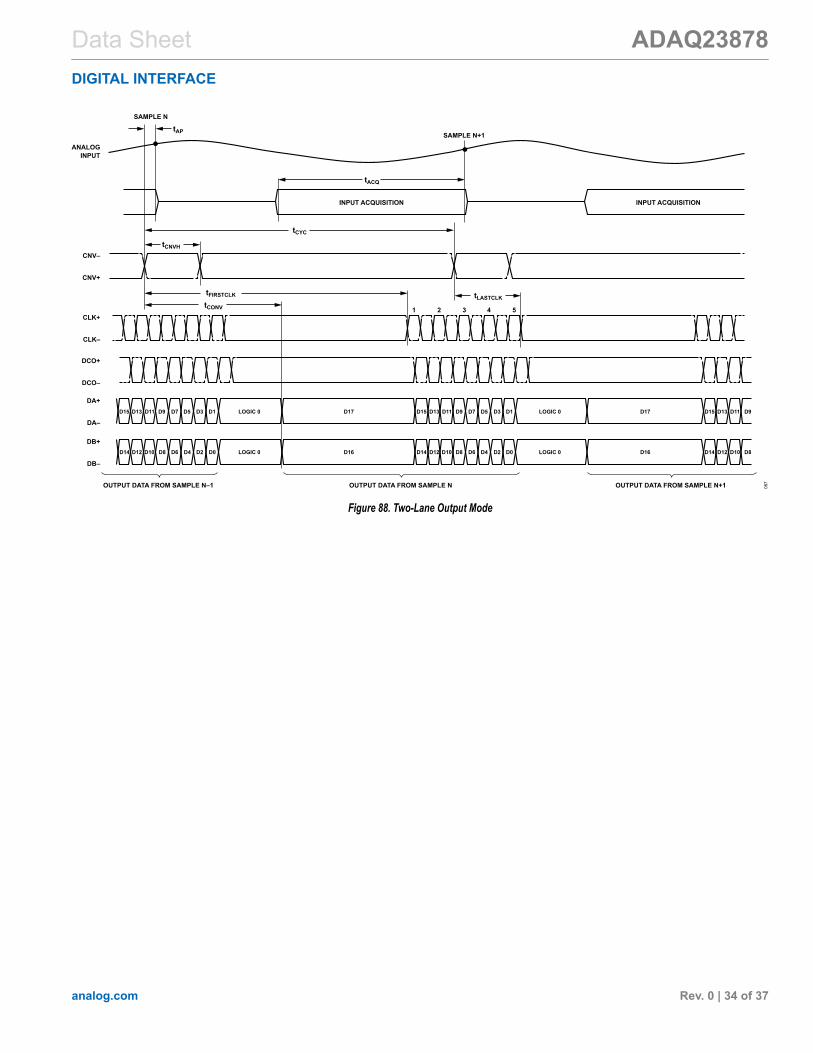
The ADAQ23878 conversion is controlled by the CNV+ and CNV–inputs, which can be driven directly with an LVDS signal. Alterna-tively, the CNV+ pin can be driven with a 0 V to 2.5 V CMOS signalwhen CNV– is connected to GND. A rising edge on CNV+ samplesthe analog inputs and initiates a conversion. The pulse width ofCNV+ must meet the tCNVH and tCNVL specifications in the timingtable (see Table 2).After the ADAQ23878 is powered on or exits power-down mode,conversion data is invalid for the first two conversion cycles. Thesubsequent conversion results are accurate as long as the timebetween conversions meets the tCYC specification. If the analoginput signal has not completely settled when it is sampled, theADAQ23878 noise performance is affected by jitter on the risingedge of CNV+. In this case, drive the rising edge of CNV+ with aclean, low jitter signal. Note that the ADAQ23878 is less sensitive tojitter on the falling edge of CNV+. In applications that are insensitiveto jitter, CNV can be driven directly from a field programmable gatearray (FPGA).The ADAQ23878 has an internal clock that is trimmed to achieve amaximum conversion time of 63 ns. With a typical acquisition timeof 27.7 ns, throughput performance of 15 MSPS is achieved.The ADAQ23878 has a serial LVDS digital interface that is easy toconnect to an FPGA. Three LVDS pairs are required: CLK±, DCO±,and DA±. A fourth LVDS pair, DB±, is optional (see Figure 84).Route the LVDS signals on the PCB as 100 Ω differential transmis-sion lines and terminated at the receiver with 100 Ω resistors. Theoptional LVDS output, DB±, is enabled, and data is output two bitsat a time on DA± and DB±. Enabling the DB± output increases thesupply current from VIO by about 3.6 mA. In two-lane mode, fourclock pulses are required for CLK± (see Figure 88).
Figure 84. Digital Output Interface to an FPGA
ONE-LANE OUTPUT MODEA conversion is started by the rising edge of CNV+. When theconversion is complete, the most significant data bit is output onDA±. Data is then ready to be shifted out by applying a burst ofeight clock pulses to the CLK± input. The data on DA± is updatedby every edge of CLK±. An echoed version of CLK± is output onDCO±. The edges of DA± and DCO± are aligned. Therefore, DCO±can be used to latch DA± in the FPGA. The timing of a singleconversion is shown in Figure 85 and Figure 86. Data must beclocked out after the current conversion is complete, and beforethe next conversion finishes. The valid time window for clocking outdata is shown in Figure 87. Note that it is allowed to be still clockingout data when the next conversion begins.
TWO-LANE OUTPUT MODEAt high sample rates, the required LVDS interface data rate canreach >400 Mbps. Most FPGAs can support this rate, but if a lowerdata rate is desired, the two-lane output mode can be used. Whenthe TWOLANES input pin is connected high (VIO), the ADAQ23878outputs two bits at a time on DA−/DA+ and DB−/DB+, as shown inFigure 88.

Data Sheet ADAQ23878DIGITAL INTERFACE
analog.com Rev. 0 | 33 of 37
Figure 85. Timing Diagram for a Single Conversion in One-Lane Mode
Figure 86. Timing Diagram for Multiple Conversions in One-Lane Output Mode
Figure 87. Valid Time Window for Clocking Out Data
Data Sheet ADAQ23878DIGITAL INTERFACE
analog.com Rev. 0 | 34 of 37
Figure 88. Two-Lane Output Mode

Data Sheet ADAQ23878DIGITAL INTERFACE
analog.com Rev. 0 | 35 of 37
OUTPUT TEST PATTERNSThe test pattern is enabled when the TESTPAT pin is broughthigh (VIO) to allow in-circuit testing of the digital interface ofthe ADAQ23878 and forces the LVDS data outputs to be a testpattern. The ADAQ23878 digital data outputs known values as atest pattern as follows:
One-lane mode: 10 1000 0001 1111 1100 Two-lane mode: 11 0011 0000 1111 1100
When the TESTPAT pin is connected low (GND), the ADAQ23878digital data outputs the conversion results.

Data Sheet ADAQ23878BOARD LAYOUT
analog.com Rev. 0 | 36 of 37
The PCB layout is critical for preserving signal integrity and achiev-ing the expected performance from the ADAQ23878. A multilayerboard with an internal, clean ground plane in the first layer beneaththe ADAQ23878 is recommended. Care must be taken with theplacement of individual components and routing of various signalson the board. It is highly recommended to route input and outputsignals symmetrically. Solder the ground pins of the ADAQ23878directly to the ground plane of the PCB using multiple vias. Removethe ground and power planes beneath the input and output pinsof ADAQ23878 to avoid undesired parasitic capacitance. Any unde-sired parasitic capacitance could impact the distortion and linearityperformance of the ADAQ23878.The pinout of the ADAQ23878 eases the layout and allowing itsanalog signals on the left side and its digital signals on the rightside. The sensitive analog and digital sections must be separatedon the PCB while keeping the power supply circuitry away from theanalog signal path. Fast switching signals, such as CNV± or CLK±,and digital outputs DA± and DB± must not run near or cross overanalog signal paths to prevent noise coupling to the ADAQ23878.Good quality ceramic bypass capacitors of at least 2.2 µF (0402,X5R) must be placed between each of supply pins (VDD, VIO, VS+,and VS−) of the ADAQ23878 and GND to minimize electromagneticinterference (EMI) susceptibility and to reduce the effect of glitcheson the power supply lines. All the other required bypass capacitorsare laid out within the ADAQ23878, saving extra board space andcost.Figure 89 shows the FFT sampling of the ADAQ23878 at 15 MSPSwith the inputs shorted when the external decoupling capacitors onthe REFIN, VDD, and VIO pins near the µModule are removed andhow well µModule rejects any supply noise and reduces sensitivity
to perturbations. This performance impact was verified on theEVAL-ADAQ23878FMCZ and no spurs are present in the noisefloor, regardless of whether these external decoupling capacitorsare used or removed. The recommended board layout is describedin the EVAL-ADAQ23878FMCZ user guide.
Figure 89. FFT with Shorted Inputs
MECHANICAL STRESS SHIFTThe mechanical stress of mounting a device to a board may causesubtle changes to the SNR and internal voltage reference. The bestsoldering method is to use IR reflow or convection soldering with acontrolled temperature profile. Hand soldering with a heat gun or asoldering iron is not recommended.
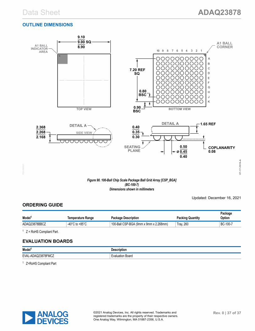
Data Sheet ADAQ23878OUTLINE DIMENSIONS
©2021 Analog Devices, Inc. All rights reserved. Trademarks andregistered trademarks are the property of their respective owners.One Analog Way, Wilmington, MA 01887-2356, U.S.A.
Rev. 0 | 37 of 37
Figure 90. 100-Ball Chip Scale Package Ball Grid Array [CSP_BGA](BC-100-7)
Dimensions shown in millimeters
Updated: December 16, 2021
ORDERING GUIDE
Model1 Temperature Range Package Description Packing QuantityPackageOption
ADAQ23878BBCZ -40°C to +85°C 100-Ball CSP-BGA (9mm x 9mm x 2.268mm) Tray, 260 BC-100-71 Z = RoHS Compliant Part.
EVALUATION BOARDSModel1 DescriptionEVAL-ADAQ23878FMCZ Evaluation Board1 Z=RoHS Compliant Part