16-bit, 1 msps μmodule data acquisition system … 1 msps μmodule data acquisition system data...
TRANSCRIPT

16-Bit, 1 MSPS μModule Data Acquisition System
Data Sheet ADAQ7980/ADAQ7988
Rev. A Document Feedback Information furnished by Analog Devices is believed to be accurate and reliable. However, no responsibility is assumed by Analog Devices for its use, nor for any infringements of patents or other rights of third parties that may result from its use. Specifications subject to change without notice. No license is granted by implication or otherwise under any patent or patent rights of Analog Devices. Trademarks and registered trademarks are the property of their respective owners.
One Technology Way, P.O. Box 9106, Norwood, MA 02062-9106, U.S.A.Tel: 781.329.4700 ©2017 Analog Devices, Inc. All rights reserved. Technical Support www.analog.com
FEATURES Easy to use
μModule data acquisition system All active components designed by Analog Devices, Inc. 50% PCB area savings Includes critical passive components
SPI-/QSPI-/MICROWIRE™-/DSP-compatible serial interface Daisy-chain multiple ADAQ7980/ADAQ7988 devices Versatile supply configuration with 1.8 V/2.5 V/3 V/5 V
logic interface High performance
16-bit resolution with no missing codes Throughput: 1 MSPS (ADAQ7980) and 500 kSPS (ADAQ7988) INL: ±8 ppm typical and 20 ppm maximum SNR: 91.5 dB typical at 10 kHz (unity gain) THD: −105 dB at 10 kHz Zero error: ±0.06 mV typical (unity gain) Zero error temperature drift: 1.3 μV/°C maximum
Low power dissipation 21 mW typical at 1 MSPS (ADAQ7980) 16.5 mW typical at 500 kSPS (ADAQ7988) Flexible power-down modes
Small, 24-lead, 5 mm × 4 mm LGA package Excellent ESD ratings
3500 V human body model (HBM) 1250 V field-induced charged device model (FICDM)
Wide operating temperature range: −55°C to +125°C
APPLICATIONS Automated test equipment (ATE) Battery powered instrumentation Communications Data acquisition Process control Medical instruments GENERAL DESCRIPTION The ADAQ7980/ADAQ7988 are 16-bit analog-to-digital converter (ADC) μModule® data acquisition systems that integrate four common signal processing and conditioning blocks into a system in package (SiP) design that supports a variety of applications. These devices contain the most critical passive components, eliminating many of the design challenges associated with traditional signal chains that use successive approximation register (SAR) ADCs. These passive components are crucial to achieving the specified device performance.
FUNCTIONAL BLOCK DIAGRAM REF
GND
VDD
VIO
SDI
SCK
SDO
CNV
20Ω
V+
V–
1.8nF
LDO
2.2µF10µF
REF_OUT LDO_OUT
PD_REF
AMP_OUT
PD_AMP
PD_LDO
ADC
ADCN
IN+
IN–
ADAQ7980/ADAQ7988
1506
0-00
1
Figure 1.
The ADAQ7980/ADAQ7988 contain a high accuracy, low power, 16-bit SAR ADC, a low power, high bandwidth, high input impedance ADC driver, a low power, stable reference buffer, and an efficient power management block. Housed within a tiny, 5 mm × 4 mm LGA package, these products simplify the design process for data acquisition systems. The level of system integration of the ADAQ7980/ADAQ7988 solves many design challenges, while the devices still provide the flexibility of a configurable ADC driver feedback loop to allow gain and/or common-mode adjustments. A set of four device supplies provides optimal system performance; however, single-supply operation is possible with minimal impact on device operating specifications.
The ADAQ7980/ADAQ7988 integrate within a compact, integrated circuit (IC)-like form factor key components commonly used in data acquisition signal chain designs. The μModule family transfers the design burden of component selection, optimization, and layout from designer to device, shortening overall design time, system troubleshooting, and ultimately improving time to market.
The serial peripheral interface (SPI)-compatible serial interface features the ability to daisy-chain multiple devices on a single, 3-wire bus and provides an optional busy indicator. The user interface is compatible with 1.8 V, 2.5 V, 3 V, or 5 V logic.
Specified operation of these devices is from −55°C to +125°C.
Table 1. Integrated SAR ADC μModules Type 500 kSPS 1000 kSPS 16-Bit ADAQ7988 ADAQ7980
ADAQ7980/ADAQ7988 Data Sheet
Rev. A | Page 2 of 49
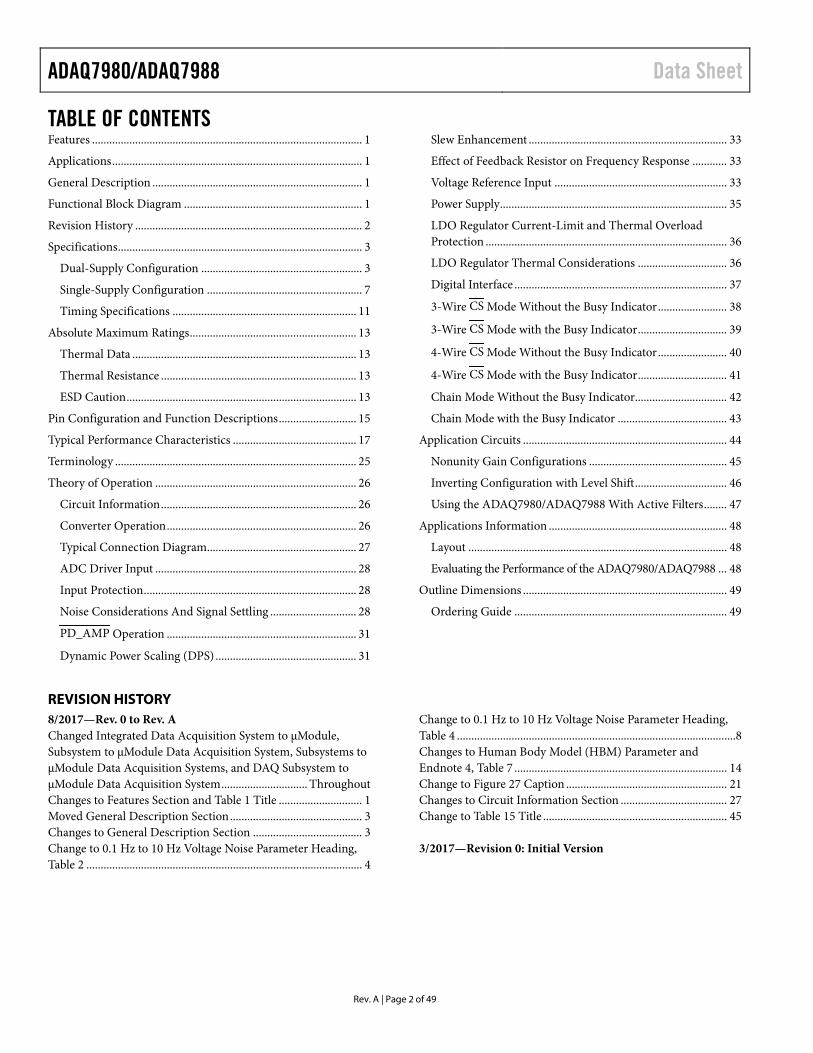
TABLE OF CONTENTS Features .............................................................................................. 1
Applications ....................................................................................... 1
General Description ......................................................................... 1
Functional Block Diagram .............................................................. 1
Revision History ............................................................................... 2
Specifications ..................................................................................... 3
Dual-Supply Configuration ........................................................ 3
Single-Supply Configuration ...................................................... 7
Timing Specifications ................................................................ 11
Absolute Maximum Ratings .......................................................... 13
Thermal Data .............................................................................. 13
Thermal Resistance .................................................................... 13
ESD Caution ................................................................................ 13
Pin Configuration and Function Descriptions ........................... 15
Typical Performance Characteristics ........................................... 17
Terminology .................................................................................... 25
Theory of Operation ...................................................................... 26
Circuit Information .................................................................... 26
Converter Operation .................................................................. 26
Typical Connection Diagram.................................................... 27
ADC Driver Input ...................................................................... 28
Input Protection .......................................................................... 28
Noise Considerations And Signal Settling .............................. 28
PD_AMP Operation .................................................................. 31
Dynamic Power Scaling (DPS) ................................................. 31
Slew Enhancement ..................................................................... 33
Effect of Feedback Resistor on Frequency Response ............ 33
Voltage Reference Input ............................................................ 33
Power Supply ............................................................................... 35
LDO Regulator Current-Limit and Thermal Overload Protection .................................................................................... 36
LDO Regulator Thermal Considerations ............................... 36
Digital Interface .......................................................................... 37
3-Wire CS Mode Without the Busy Indicator ........................ 38
3-Wire CS Mode with the Busy Indicator ............................... 39
4-Wire CS Mode Without the Busy Indicator ........................ 40
4-Wire CS Mode with the Busy Indicator ............................... 41
Chain Mode Without the Busy Indicator................................ 42
Chain Mode with the Busy Indicator ...................................... 43
Application Circuits ....................................................................... 44
Nonunity Gain Configurations ................................................ 45
Inverting Configuration with Level Shift ................................ 46
Using the ADAQ7980/ADAQ7988 With Active Filters ........ 47
Applications Information .............................................................. 48
Layout .......................................................................................... 48
Evaluating the Performance of the ADAQ7980/ADAQ7988 ... 48
Outline Dimensions ....................................................................... 49
Ordering Guide .......................................................................... 49
REVISION HISTORY 8/2017—Rev. 0 to Rev. A Changed Integrated Data Acquisition System to μModule, Subsystem to μModule Data Acquisition System, Subsystems to μModule Data Acquisition Systems, and DAQ Subsystem to μModule Data Acquisition System .............................. Throughout Changes to Features Section and Table 1 Title ............................. 1 Moved General Description Section .............................................. 3 Changes to General Description Section ...................................... 3 Change to 0.1 Hz to 10 Hz Voltage Noise Parameter Heading, Table 2 ................................................................................................ 4
Change to 0.1 Hz to 10 Hz Voltage Noise Parameter Heading, Table 4 ................................................................................................. 8 Changes to Human Body Model (HBM) Parameter and Endnote 4, Table 7 .......................................................................... 14 Change to Figure 27 Caption ........................................................ 21 Changes to Circuit Information Section ..................................... 27 Change to Table 15 Title ................................................................ 45 3/2017—Revision 0: Initial Version
ADAQ7980/ADAQ7988 Data Sheet
Rev. A | Page 3 of 49
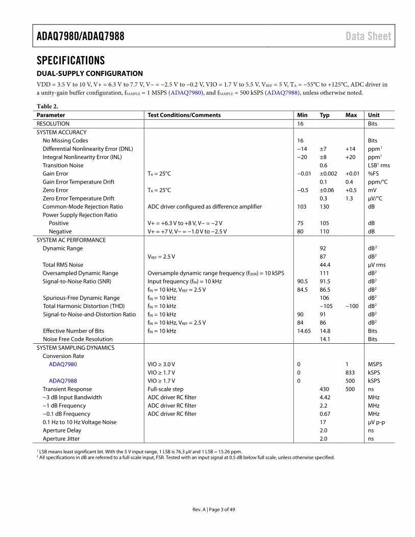
SPECIFICATIONS DUAL-SUPPLY CONFIGURATION VDD = 3.5 V to 10 V, V+ = 6.3 V to 7.7 V, V− = −2.5 V to −0.2 V, VIO = 1.7 V to 5.5 V, VREF = 5 V, TA = −55°C to +125°C, ADC driver in a unity-gain buffer configuration, fSAMPLE = 1 MSPS (ADAQ7980), and fSAMPLE = 500 kSPS (ADAQ7988), unless otherwise noted.
Table 2. Parameter Test Conditions/Comments Min Typ Max Unit RESOLUTION 16 Bits SYSTEM ACCURACY
No Missing Codes 16 Bits Differential Nonlinearity Error (DNL) −14 ±7 +14 ppm1 Integral Nonlinearity Error (INL) −20 ±8 +20 ppm1 Transition Noise 0.6 LSB1 rms Gain Error TA = 25°C −0.01 ±0.002 +0.01 %FS Gain Error Temperature Drift 0.1 0.4 ppm/°C Zero Error TA = 25°C −0.5 ±0.06 +0.5 mV Zero Error Temperature Drift 0.3 1.3 µV/°C Common-Mode Rejection Ratio ADC driver configured as difference amplifier 103 130 dB Power Supply Rejection Ratio
Positive V+ = +6.3 V to +8 V, V− = −2 V 75 105 dB Negative V+ = +7 V, V− = −1.0 V to −2.5 V 80 110 dB
SYSTEM AC PERFORMANCE Dynamic Range 92 dB2 VREF = 2.5 V 87 dB2 Total RMS Noise 44.4 µV rms Oversampled Dynamic Range Oversample dynamic range frequency (fODR) = 10 kSPS 111 dB2 Signal-to-Noise Ratio (SNR) Input frequency (fIN) = 10 kHz 90.5 91.5 dB2 fIN = 10 kHz, VREF = 2.5 V 84.5 86.5 dB2 Spurious-Free Dynamic Range fIN = 10 kHz 106 dB2 Total Harmonic Distortion (THD) fIN = 10 kHz −105 −100 dB2 Signal-to-Noise-and-Distortion Ratio fIN = 10 kHz 90 91 dB2 fIN = 10 kHz, VREF = 2.5 V 84 86 dB2 Effective Number of Bits fIN = 10 kHz 14.65 14.8 Bits Noise Free Code Resolution 14.1 Bits
SYSTEM SAMPLING DYNAMICS Conversion Rate
ADAQ7980 VIO ≥ 3.0 V 0 1 MSPS VIO ≥ 1.7 V 0 833 kSPS
ADAQ7988 VIO ≥ 1.7 V 0 500 kSPS Transient Response Full-scale step 430 500 ns −3 dB Input Bandwidth ADC driver RC filter 4.42 MHz −1 dB Frequency ADC driver RC filter 2.2 MHz −0.1 dB Frequency ADC driver RC filter 0.67 MHz 0.1 Hz to 10 Hz Voltage Noise 17 µV p-p Aperture Delay 2.0 ns Aperture Jitter 2.0 ns
1 LSB means least significant bit. With the 5 V input range, 1 LSB is 76.3 µV and 1 LSB = 15.26 ppm. 2 All specifications in dB are referred to a full-scale input, FSR. Tested with an input signal at 0.5 dB below full scale, unless otherwise specified.
ADAQ7980/ADAQ7988 Data Sheet
Rev. A | Page 4 of 49
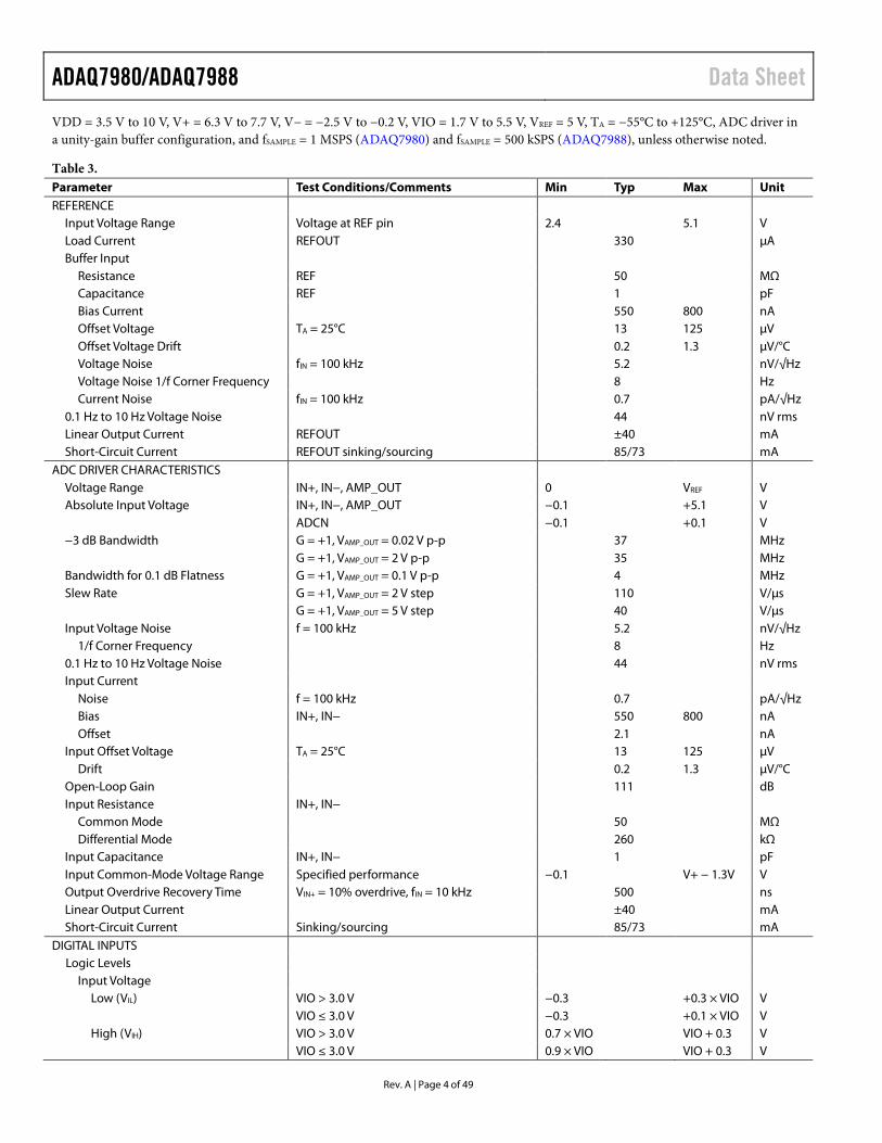
VDD = 3.5 V to 10 V, V+ = 6.3 V to 7.7 V, V− = −2.5 V to −0.2 V, VIO = 1.7 V to 5.5 V, VREF = 5 V, TA = −55°C to +125°C, ADC driver in a unity-gain buffer configuration, and fSAMPLE = 1 MSPS (ADAQ7980) and fSAMPLE = 500 kSPS (ADAQ7988), unless otherwise noted.
Table 3. Parameter Test Conditions/Comments Min Typ Max Unit REFERENCE
Input Voltage Range Voltage at REF pin 2.4 5.1 V Load Current REFOUT 330 µA Buffer Input
Resistance REF 50 MΩ Capacitance REF 1 pF Bias Current 550 800 nA Offset Voltage TA = 25°C 13 125 µV Offset Voltage Drift 0.2 1.3 µV/°C Voltage Noise fIN = 100 kHz 5.2 nV/√Hz Voltage Noise 1/f Corner Frequency 8 Hz Current Noise fIN = 100 kHz 0.7 pA/√Hz
0.1 Hz to 10 Hz Voltage Noise 44 nV rms Linear Output Current REFOUT ±40 mA Short-Circuit Current REFOUT sinking/sourcing 85/73 mA
ADC DRIVER CHARACTERISTICS Voltage Range IN+, IN−, AMP_OUT 0 VREF V Absolute Input Voltage IN+, IN−, AMP_OUT −0.1 +5.1 V ADCN −0.1 +0.1 V −3 dB Bandwidth G = +1, VAMP_OUT = 0.02 V p-p 37 MHz G = +1, VAMP_OUT = 2 V p-p 35 MHz Bandwidth for 0.1 dB Flatness G = +1, VAMP_OUT = 0.1 V p-p 4 MHz Slew Rate G = +1, VAMP_OUT = 2 V step 110 V/µs G = +1, VAMP_OUT = 5 V step 40 V/µs Input Voltage Noise f = 100 kHz 5.2 nV/√Hz
1/f Corner Frequency 8 Hz 0.1 Hz to 10 Hz Voltage Noise 44 nV rms Input Current
Noise f = 100 kHz 0.7 pA/√Hz Bias IN+, IN− 550 800 nA Offset 2.1 nA
Input Offset Voltage TA = 25°C 13 125 µV Drift 0.2 1.3 µV/°C
Open-Loop Gain 111 dB Input Resistance IN+, IN−
Common Mode 50 MΩ Differential Mode 260 kΩ
Input Capacitance IN+, IN− 1 pF Input Common-Mode Voltage Range Specified performance −0.1 V+ − 1.3V V Output Overdrive Recovery Time VIN+ = 10% overdrive, fIN = 10 kHz 500 ns Linear Output Current ±40 mA Short-Circuit Current Sinking/sourcing 85/73 mA
DIGITAL INPUTS Logic Levels
Input Voltage Low (VIL) VIO > 3.0 V −0.3 +0.3 × VIO V
VIO ≤ 3.0 V −0.3 +0.1 × VIO V High (VIH) VIO > 3.0 V 0.7 × VIO VIO + 0.3 V
VIO ≤ 3.0 V 0.9 × VIO VIO + 0.3 V

Data Sheet ADAQ7980/ADAQ7988
Rev. A | Page 5 of 49
Parameter Test Conditions/Comments Min Typ Max Unit Input Current
Low (IIL) −1 +1 µA High (IIH) −1 +1 µA
DIGITAL OUTPUTS Data Format Serial 16 bits, straight binary Pipeline Delay Conversion results available
immediately after completed conversion
VOL ISINK = 500 µA 0.4 V VOH ISOURCE = −500 µA VIO − 0.3 V
POWER-DOWN SIGNALING ADC Driver/REF Buffer
PD_AMP, PD_REF Voltage
Low Powered down <2.2 V High Enabled >2.6 V
Turn-Off Time 50% of PD_AMP, PD_REF to <10% of enabled quiescent current
1.25 2.75 µs
Turn-On Time Specified performance 2 7.25 µs Dynamic Power Scaling Period Specified performance 10 µs
Low Dropout (LDO) Regulator PD_LDO Voltage
Low Powered down 1.06 1.12 1.18 V High Enabled 1.15 1.22 1.30 V
PD_LDO Logic Hysteresis 100 mV
Turn-Off Time 2.2 µF capacitive load 460 650 µs Turn-On Time 370 425 µs
POWER REQUIREMENTS VDD 3.5 5 10 V LDO Voltage Accuracy ILDO_OUT = 10 mA, TA = 25°C −0.8 +0.8 %
100 µA < ILDO_OUT < 100 mA, VDD = 3.5 V to 10 V
−1.8 +1.8 %
LDO Line Regulation VDD = 3.5 V to 10 V −0.015 +0.015 %/V LDO Load Regulation ILDO_OUT = 100 µA to 100 mA 0.002 0.004 %/mA LDO Start-Up Time VLDO_OUT = 2.5 V 380 µs LDO Current-Limit Threshold 250 360 460 mA LDO Thermal Shutdown
Threshold TJ rising 150 °C Hysteresis 15 °C
LDO Dropout Voltage ILDO_OUT = 10 mA 30 60 mV ILDO_OUT = 100 mA 200 420 mV V+ 3.7 7 V− + 10 V V− V+ − 10 −2 +0.1 V VIO 1.7 5.5 V Total Standby Current1, 2 Static, all devices enabled 1.2 1.7 mA ADC driver, REF buffer disable 56 103 µA ADC driver, REF buffer, LDO disable 14 23 µA ADAQ7980 Current Draw 1 MSPS
VIO 0.3 0.34 mA V+/V− 1.5 2.0 mA VDD 1.45 1.6 mA

ADAQ7980/ADAQ7988 Data Sheet
Rev. A | Page 6 of 49
Parameter Test Conditions/Comments Min Typ Max Unit ADAQ7980 Power Dissipation 1 MSPS
V+/V−/VDD 20 36 mW 1 kSPS, dynamic power scaling enabled3 5.8 9 mW
VIO 1.0 1.9 mW Total 21 37.94 mW
ADAQ7988 Current Draw VIO 0.15 0.17 mA V+/V− 1.35 1.85 mA VDD 0.73 0.8 mA
ADAQ7988 Power Dissipation 500 kSPS V+/V−/VDD 16 26.5 mW
1 kSPS, dynamic power scaling enabled3 5.8 9 mW VIO 0.5 0.95 mW Total 16.5 27.54 mW
TEMPERATURE RANGE Specified Performance TMIN to TMAX −55 +125 °C
1 With all digital inputs forced to VIO or GND as required. 2 During the acquisition phase. 3 Dynamic power scaling duty cycle is 10%. 4 Calculated with the maximum supply differential and not the typical supply values.

Data Sheet ADAQ7980/ADAQ7988
Rev. A | Page 7 of 49
SINGLE-SUPPLY CONFIGURATION VDD = V+ = 5.0 V, V− = 0 V, VIO = 1.7 V to 5.5 V, VREF = 3.3 V, TA = −55°C to +125°C, the ADC driver in a unity-gain buffer configuration, and fSAMPLE = 1 MSPS (ADAQ7980) and fSAMPLE = 500 kSPS (ADAQ7988), unless otherwise noted.
Table 4. Parameter Test Conditions/Comments Min Typ Max Unit RESOLUTION 16 Bits SYSTEM ACCURACY
Differential Nonlinearity Error1 −14 ±7 +14 ppm2 Integral Nonlinearity Error1 −20 ±8 +20 ppm2 Transition Noise 0.8 LSB2 rms Gain Error TA = 25°C −0.013 ±0.002 +0.013 %FS Gain Error Temperature Drift 0.1 0.4 ppm/°C Zero Error TA = 25°C −0.5 ±0.06 +0.5 mV Zero Error Temperature Drift 0.35 1.75 µV/°C Common-Mode Rejection Ratio 103 133 dB Power Supply Rejection Ratio
Positive V+ = 4.5 V to 5.5 V, V− = 0 V 75 92 dB SYSTEM AC PERFORMANCE
Dynamic Range 89 dB3 Total RMS Noise 41.4 µV rms Oversampled Dynamic Range fODR = 10 kSPS 109 dB3 Signal-to-Noise Ratio Input frequency (fIN) = 10 kHz 87.3 88.7 dB3 Spurious-Free Dynamic Range fIN = 10 kHz 103 dB3 Total Harmonic Distortion fIN = 10 kHz −113 −100 dB3 Signal-to-Noise-and-Distortion Ratio fIN = 10 kHz 87 88.4 dB3 Effective Number of Bits fIN = 10 kHz 14.1 14.4 Bits Noise Free Code Resolution 13.5 Bits
SYSTEM SAMPLING DYNAMICS Conversion Rate
ADAQ7980 VIO ≥ 3.0 V 0 1 MSPS VIO ≥ 1.7 V 0 833 kSPS
ADAQ7988 VIO ≥ 1.7 V 0 500 kSPS Transient Response Full-scale step 430 500 ns −3 dB Input Bandwidth ADC driver RC filter 4.42 MHz −1 dB Frequency ADC driver RC filter 2.2 MHz −0.1 dB Frequency ADC driver RC filter 0.67 MHz 0.1 Hz to 10 Hz Voltage Noise 17 µV p-p Aperture Delay 2.0 ns Aperture Jitter 2.0 ns
1 Nonlinearity guaranteed over input voltage range. Codes below 150 mV are not represented with a unipolar supply configuration. 2 LSB means least significant bit. With the 3.3 V input range, 1 LSB = 50.4 µV, and 1 LSB = 15.26 ppm. 3 All specifications in dB are referred to a full-scale input, FSR. Tested with an input signal at 0.5 dB below full scale, unless otherwise specified.

ADAQ7980/ADAQ7988 Data Sheet
Rev. A | Page 8 of 49
VDD = V+ = 5.0 V, V− = 0 V, VIO = 1.7 V to 5.5 V, VREF = 3.3 V, TA = −55°C to +125°C, the ADC driver in a unity-gain buffer configuration, and fSAMPLE = 1 MSPS (ADAQ7980) and fSAMPLE = 500 kSPS (ADAQ7988), unless otherwise noted.
Table 5. Parameter Test Conditions/Comments Min Typ Max Unit REFERENCE
Input Voltage Range Voltage at REF pin 2.4 V+ − 1.3 V Load Current REFOUT 330 µA Buffer Input
Resistance REF 50 MΩ Capacitance REF 1 pF Bias Current 470 720 nA Offset Voltage TA = 25°C 9 125 µV Offset Voltage Drift 0.2 1.5 µV/°C Voltage Noise fIN = 100kHz 5.9 nV/√Hz Voltage Noise 1/f Corner Frequency 8 Hz Current Noise fIN = 100kHz 0.6 pA/√Hz
0.1 Hz to 10 Hz Voltage Noise 54 nV rms Linear Output Current REFOUT ±40 mA Short-Circuit Current REFOUT sinking/sourcing 73/63 mA
ADC DRIVER CHARACTERISTICS Specified Voltage Range IN+, IN−, AMP_OUT 0.15 VREF V Absolute Input Voltage IN+, IN−, AMP_OUT −0.1 V+ − 1.3 V ADCN −0.1 +0.1 V −3 dB Bandwidth G = +1, VAMP_OUT = 0.02 V p-p 31 MHz G = +1, VAMP_OUT = 2 V p-p 30 MHz Bandwidth for 0.1 dB Flatness G = +1, VAMP_OUT = 0.1 V p-p 4 MHz Slew Rate G = +1, VAMP_OUT = 2 V step 31 V/µs G = +1, VAMP_OUT = 3.15 V step 20 V/µs Input Voltage Noise f = 100 kHz 5.9 nV/√Hz
1/f Corner Frequency 8 Hz 0.1 Hz to 10 Hz Voltage Noise 54 nV rms Input Current
Noise f = 100 kHz 0.6 pA/√Hz Bias IN+, IN− 470 720 nA Offset 0.4 nA
Input Offset Voltage TA = 25°C 9 125 µV Open-Loop Gain 109 dB Input Resistance IN+, IN−
Common Mode 50 MΩ Differential Mode 260 kΩ
Input Capacitance IN+, IN− 1 pF Input Common-Mode Voltage Range Specified performance −0.1 V+ − 1.3 V Output Overdrive Recovery Time VIN+ = 10% overdrive, fIN = 10 kHz 800 ns Linear Output Current ±40 mA Short-Circuit Current Sinking/sourcing 73/63 mA
DIGITAL INPUTS Logic Levels
Input Voltage Low (VIL) VIO > 3.0 V −0.3 +0.3 × VIO V
VIO ≤ 3.0 V −0.3 +0.1 × VIO V High (VIH) VIO > 3.0 V 0.7 × VIO VIO + 0.3 V
VIO ≤ 3.0 V 0.9 × VIO VIO + 0.3 V

Data Sheet ADAQ7980/ADAQ7988
Rev. A | Page 9 of 49
Parameter Test Conditions/Comments Min Typ Max Unit Input Current
Low (IIL) −1 +1 µA High (IIH) −1 +1 µA
DIGITAL OUTPUTS Data Format Serial 16 bits straight binary Pipeline Delay Conversion results available
immediately after completed conversion
VOL ISINK = 500 µA 0.4 V VOH ISOURCE = −500 µA VIO − 0.3 V
POWER-DOWN SIGNALING ADC Driver/Reference Buffer
PD_AMP, PD_REF Voltage
Low Powered down <1.5 V High Enabled >1.9 V
Turn-Off Time 50% of PD_AMP, PD_REF to <10% of enabled quiescent current
0.9 1.25 µs
Turn-On Time Specified performance 2 7.25 µs Dynamic Power Scaling Period Specified performance 10 µs
LDO PD_LDO Voltage
Low Powered down 1.06 1.12 1.18 V High Enabled 1.15 1.22 1.30 V
PD_LDO Logic Hysteresis 100 mV
Turn-Off Time 2.2 µF capacitive load 460 650 µs Turn-On Time 370 425 µs
POWER REQUIREMENTS VDD 3.5 5 10 V LDO Voltage Accuracy ILDO_OUT = 10 mA, TA = 25°C −0.8 +0.8 % 100 µA < ILDO_OUT < 100 mA, VDD = 3.5 V to 10 V −1.8 +1.8 % LDO Line Regulation VDD = 3.5 V to 10 V −0.015 +0.015 %/V LDO Load Regulation ILDO_OUT = 100 µA to 100 mA 0.002 0.004 %/mA LDO Start-Up Time VLDO_OUT = 2.5 V 380 µs LDO Current-Limit Threshold 250 360 460 mA LDO Thermal Shutdown
Threshold TJ rising 150 °C Hysteresis 15 °C
LDO Dropout Voltage ILDO_OUT = 10 mA 30 60 mV ILDO_OUT = 100 mA 200 420 mV V+ 3.7 5 V− + 10 V V− V+ − 10 0 +0.1 V VIO 1.7 5.5 V Total Standby Current1, 2 Static, all devices enabled 1.1 1.7 mA ADC driver, REF buffer disabled 50 103 µA ADC driver, REF buffer, LDO disabled 7 23 µA ADAQ7980 Current Draw 1 MSPS
VIO 0.3 0.34 mA V+/V− 1.3 2.0 mA VDD 1.45 1.6 mA

ADAQ7980/ADAQ7988 Data Sheet
Rev. A | Page 10 of 49
Parameter Test Conditions/Comments Min Typ Max Unit ADAQ7980 Power Dissipation 1MSPS
V+/V−/VDD 13.75 36 mW 1 kSPS, ADC driver dynamic power scaling enabled3 2.9 9 mW
VIO 1.0 1.9 mW Total 14.75 37.94 mW
ADAQ7988 Current Draw VIO 0.15 0.17 mA V+/V− 1.15 1.85 mA VDD 0.73 0.8 mA
ADAQ7988 Power Dissipation 500 kSPS V+/V−/VDD 9.4 26.5 mW
1 kSPS, ADC driver dynamic power scaling enabled3 2.9 9 mW VIO 0.5 0.95 mW Total 9.9 27.54 mW
TEMPERATURE RANGE Specified Performance TMIN to TMAX −55 +125 °C
1 With all digital inputs forced to VIO or GND as required. 2 During the acquisition phase. 3 Dynamic power scaling duty cycle is 10%. 4 Calculated with the maximum supply differential and not the typical supply values.

Data Sheet ADAQ7980/ADAQ7988
Rev. A | Page 11 of 49
TIMING SPECIFICATIONS VDD = 3.5 V to 10 V, VIO = 1.7 V to 5.5 V, and TA = −55°C to +125°C, unless otherwise noted In addition to Figure 2 and Figure 3, see Figure 72, Figure 74, Figure 76, Figure 78, Figure 80, and Figure 82 for the additional timing diagrams detailed in Table 6.
Table 6. Parameter Symbol Min Typ Max Unit CONVERSION TIME: CNV RISING EDGE TO DATA AVAILABLE tCONV
VIO Above 3.0 V (ADAQ7980) 500 710 ns VIO Above 1.7 V (ADAQ7980) 500 800 ns ADAQ7988 500 1200 ns
ACQUISITION PHASE1 tACQ ns ADAQ7980 290 ns ADAQ7988 800 ns
TIME BETWEEN CONVERSIONS tCYC VIO Above 3.0 V (ADAQ7980) 1000 ns VIO Above 1.7 V (ADAQ7980) 1200 ns VIO Above 1.7 V (ADAQ7988) 2000 ns
CS MODE
CNV Pulse Width tCNVH 10 ns SCK Period tSCK
VIO Above 4.5 V 10.5 ns VIO Above 3.0 V 12 ns VIO Above 1.7 V 22 ns
CNV or SDI Low to SDO D15 MSB Valid tEN VIO Above 3.0 V 10 ns VIO Above 1.7 V 40 ns
CNV or SDI High or Last SCK Falling Edge to SDO High Impedance tDIS 20 ns SDI Valid Hold Time from CNV Rising Edge tHSDICNV
VIO Above 3.0 V 2 ns VIO Above 1.7 V 10 ns
CHAIN MODE SCK Period tSCK
VIO Above 4.5 V 11.5 ns VIO Above 3.0 V 13 ns VIO Above 1.7 V 23 ns
SDI Valid Hold Time from CNV Rising Edge tHSDICNV 0 ns SCK Valid Setup Time from CNV Rising Edge tSSCKCNV 5 ns SCK Valid Hold Time from CNV Rising Edge tHSCKCNV 5 ns SDI Valid Setup Time from SCK Falling Edge tSSDISCK 2 ns SDI Valid Hold Time from SCK Falling Edge tHSDISCK 3 ns SDI High to SDO High (with Busy Indicator) tDSDOSDI
VIO Above 3.0 V 15 ns VIO Above 1.7 V 22 ns
SCK Low Time tSCKL
VIO Above 3.0 V 4.5 ns VIO Above 1.7 V 6 ns
High Time tSCKH VIO Above 3.0 V 4.5 ns VIO Above 1.7 V 6 ns

ADAQ7980/ADAQ7988 Data Sheet
Rev. A | Page 12 of 49
Parameter Symbol Min Typ Max Unit Falling Edge to Data Remains Valid tHSDO 3 ns Falling Edge to Data Valid Delay tDSDO
VIO Above 4.5 V 9.5 ns VIO Above 3.0 V 11 ns VIO Above 1.7 V 21 ns
SDI VALID SETUP TIME From CNV RISING EDGE tSSDICNV 5 ns 1 The acquisition phase is the time available for the ADC sampling capacitors to acquire a new input with the ADC running at a throughput rate of 1 MSPS.
500µA IOL
500µA IOH
1.4VTO SDOCL
20pF
1506
0-00
2
Figure 2. Load Circuit for Digital Interface Timing
X% VIO1Y% VIO1
VIH2
VIL2VIL2VIH2
tDELAY tDELAY
1FOR VIO ≤ 3.0V, X = 90, AND Y = 10; FOR VIO > 3.0V, X = 70, AND Y = 30.2MINIMUM VIH AND MAXIMUM VIL USED. SEE DIGITAL INPUTSSPECIFICATIONS IN TABLE 3 OR TABLE 5. 15
060-
003
Figure 3. Voltage Levels for Timing

Data Sheet ADAQ7980/ADAQ7988
Rev. A | Page 13 of 49
ABSOLUTE MAXIMUM RATINGS TA = 25°C, unless otherwise noted.
Table 7. Parameter Rating V+ to V− 11 V V+ to GND −0.3 V to +11 V V− to GND −11 V to +0.3 V VDD to GND −0.3 V to +24 V REF_OUT/VIO to GND −0.3 V to +6 V IN+/IN−/REF to GND V− − 0.7 V to V+ + 0.7 V AMP_OUT/ADCN to GND −0.3 V to VREF + 0.3 V or
±130 mA Differential Analog Input Voltage
(IN+ − IN−) ±1 V
Digital Input1 Voltage to GND −0.3 V to VIO + 0.3 V Digital Output2 Voltage to GND −0.3 V to VIO + 0.3 V Input Current to Any Pin Except Supplies3, 4 ±10 mA Operating Temperature Range −55°C to +125°C Storage Temperature Range −65°C to +150°C Junction Temperature 150°C ESD
Human Body Model (HBM) 3500 V Field Induced Charged Device Model
(FICDM) 1250 V
1 The digital input pins include the following: CNV, SDI, and SCK. 2 The digital output pin is SDO. 3 Transient currents of up to 100 mA do not cause SCR latch-up. 4 Condition applies when power is provided to the device.
Stresses at or above those listed under Absolute Maximum Ratings may cause permanent damage to the product. This is a stress rating only; functional operation of the product at these or any other conditions above those indicated in the operational section of this specification is not implied. Operation beyond the maximum operating conditions for extended periods may affect product reliability.
THERMAL DATA Absolute maximum ratings apply individually only, not in combination. The ADAQ7980/ADAQ7988 can be damaged when the junction temperature (TJ) limits are exceeded. Monitoring ambient temperature does not guarantee that TJ is within the specified temperature limits. In applications with high power dissipation and poor thermal resistance, the maximum ambient temperature (TA) may have to be derated.
In applications with moderate power dissipation and low printed circuit board (PCB) thermal resistance, the maximum TA can exceed the maximum limit as long as the junction temperature is within specification limits. The θJA of the package is based on modeling and calculation using a 4-layer board. The θJA is highly dependent on the application and board layout. In applications where high maximum power dissipation exists, close attention to thermal board design is required. The θJA value may vary depending on PCB material, layout, and environmental conditions.
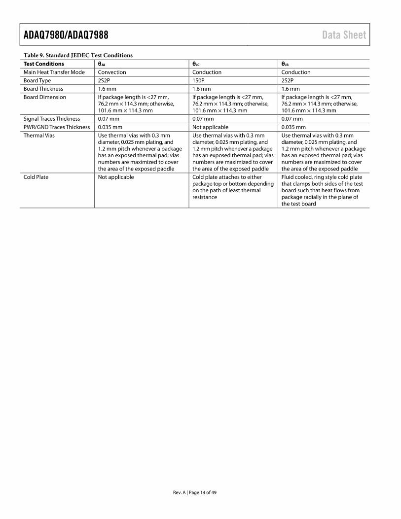
THERMAL RESISTANCE Thermal resistance values specified in Table 8 were calculated based on JEDEC specifications and must be used in compliance with JESD51-12. Because the product contains more than one silicon device, only the worst case junction temperature is reported.
Table 8. Thermal Resistance Package Type1, 2 θJA θJC TOP
2 ΨJT Unit CC-24-2 65 103 12.6 ˚C/W
1 These values represent the worst case die junction in the package. 2 Table 8 values were calculated based on the standard JEDEC test conditions
defined in Table 9, unless otherwise specified. 3 For θJC test, 100 µm thermal interface material (TIM) was used. TIM is
assumed to be 3.6 W/mK.
Only use θJA and θJC TOP to compare thermal performance of the package of the device with other semiconductor packages when all test conditions listed are similar. One common mistake is to use θJA and θJC to estimate the junction temperature in the system environment. Instead, using ΨJT is a more appropriate way to estimate the worst case junction temperature of the device in the system environment. First, take an accurate thermal measurement of the top center of the device (on the mold compound in this case) while the device operates in the system environment. This measurement is known in the following equation as TTOP. This equation can then be used to solve for the worst case TJ in that given environment as follows:
TJ = ΨJT × P + TTOP
where: ΨJT is the junction to top thermal characterization number as specified in data sheet. P refers to total power dissipation in the chip (W). TTOP refers to the package top temperature (°C) and is measured at the top center of the package in the environment of the user.
ESD CAUTION
ADAQ7980/ADAQ7988 Data Sheet
Rev. A | Page 14 of 49
Table 9. Standard JEDEC Test Conditions Test Conditions θJA θJC θJB Main Heat Transfer Mode Convection Conduction Conduction Board Type 2S2P 1S0P 2S2P Board Thickness 1.6 mm 1.6 mm 1.6 mm Board Dimension If package length is <27 mm,
76.2 mm × 114.3 mm; otherwise, 101.6 mm × 114.3 mm
If package length is <27 mm, 76.2 mm × 114.3 mm; otherwise, 101.6 mm × 114.3 mm
If package length is <27 mm, 76.2 mm × 114.3 mm; otherwise, 101.6 mm × 114.3 mm
Signal Traces Thickness 0.07 mm 0.07 mm 0.07 mm PWR/GND Traces Thickness 0.035 mm Not applicable 0.035 mm Thermal Vias Use thermal vias with 0.3 mm
diameter, 0.025 mm plating, and 1.2 mm pitch whenever a package has an exposed thermal pad; vias numbers are maximized to cover the area of the exposed paddle
Use thermal vias with 0.3 mm diameter, 0.025 mm plating, and 1.2 mm pitch whenever a package has an exposed thermal pad; vias numbers are maximized to cover the area of the exposed paddle
Use thermal vias with 0.3 mm diameter, 0.025 mm plating, and 1.2 mm pitch whenever a package has an exposed thermal pad; vias numbers are maximized to cover the area of the exposed paddle
Cold Plate Not applicable Cold plate attaches to either package top or bottom depending on the path of least thermal resistance
Fluid cooled, ring style cold plate that clamps both sides of the test board such that heat flows from package radially in the plane of the test board

Data Sheet ADAQ7980/ADAQ7988
Rev. A | Page 15 of 49
PIN CONFIGURATION AND FUNCTION DESCRIPTIONS
IN+
CNV
1
IN– 2
AMP_OUT 3
ADCN 4
GND 5
GN
D
GN
D V–
GN
D
PD_R
EF
PD_A
MP
LDO
_OU
T
13
SDO14
SCK15
SDI16
VIO17
ADAQ7980/ADAQ7988
TOP VIEW(Not to Scale)
GN
D
18
PD_L
DO
19
VDD
20
V+
21
GN
D
22
REF
23
REF
_OU
T
24
6 7 8 9 10 11 12
1506
0-00
4
Figure 4. Pin Configuration
Table 10. Pin Function Descriptions Pin No. Mnemonic Type1 Description 1 IN+ AI ADC Driver Noninverting Input. 2 IN− AI ADC Driver Inverting Input. 3 AMP_OUT AI, AO ADC Driver Output and ADC Input Before Low-Pass Filter (LPF). 4 ADCN AI Analog Input Ground Sense. Connect this pin to the analog ground plane or to a remote sense ground. 5 to 7, 9, 18, 22
GND P Ground.
8 V− P Negative Power Supply Line for the ADC Driver. This pin requires a 100 nF capacitor to GND for best operation. Connect this pin to ground for single-supply operation.
10 PD_REF DI Active Low Power-Down Signal for Reference Buffer. When powered down, the reference buffer output enters a high impedance (high-Z) state.
11 PD_AMP DI Active Low Power-Down Signal for ADC Driver. When powered down, the reference buffer output enters a high-Z state.
12 LDO_OUT P Regulated 2.5 Output Voltage from On-Board LDO. An internal 2.2 μF bypass capacitor to GND is provided.
13 CNV DI Convert Input. This input has multiple functions. On its leading edge, it initiates the conversions and selects the interface mode of the device, chain, or CS mode. In CS mode, it enables the SDO pin when low. In chain mode, read the data when CNV is high.
14 SDO DO Serial Data Output. The conversion result is output on this pin. SDO synchronizes with SCK. 15 SCK DI Serial Data Clock Input. When the device is selected, the conversion result is shifted out onto SDO by
this clock. 16 SDI DI Serial Data Input. This input provides multiple features. It selects the interface mode of the ADC as
follows. When SDI is low during the CNV rising edge, chain mode is selected. In this mode, SDI is used as a
data input to daisy-chain the conversion results of two or more ADCs onto a single SDO line. The digital data level on SDI is output on SDO with a delay of 16 SCK cycles.
When SDI is high during the CNV rising edge, CS mode is selected. In this mode, either SDI or CNV can enable the serial output signals when low; if SDI or CNV is low when the conversion is complete, the busy indicator feature is enabled.
17 VIO P Input/Output Interface Digital Power. VIO is nominally at the same supply as the host interface (1.8 V, 2.5 V, 3 V, or 5 V).
19 PD_LDO DI Active Low Power-Down Signal for LDO. When powered down, the LDO output enters a high-Z state. For a continuously enabled state or for automatic startup, tie PD_LDO to the VDD pin (Pin 20).
20 VDD P Regulator Input Supply. Bypass VDD to GND with a 2.2 μF capacitor.

ADAQ7980/ADAQ7988 Data Sheet
Rev. A | Page 16 of 49
Pin No. Mnemonic Type1 Description 21 V+ P Positive Power Supply Line for the ADC Driver and Reference Buffer. This pin can be tied to VDD as
long as headroom for the reference buffer is maintained. This pin requires a 100 nF capacitor to GND for best operation.
23 REF AI External Reference Signal. REF is the noninverting input of on-board reference buffer. Connect an external reference source to this pin. A low-pass filter may be required between the reference source and this pin to band limit noise generated by the reference source.
24 REF_OUT AO Reference Buffer Output. This pin provides access to the buffered reference signal presented to the ADC.
1 AI is analog input, AO is analog output, P is power, DI is digital input, and DO is digital output.

Data Sheet ADAQ7980/ADAQ7988
Rev. A | Page 17 of 49
TYPICAL PERFORMANCE CHARACTERISTICS VDD = 3.5 V to 10 V, V+ = 6.3 V to 7.7 V, V− = −1.0 V to −2.5 V, VIO = 1.7 V to 5.5 V, VREF = 5 V, TA = 25°C, ADC driver in a unity-gain buffer configuration, fSAMPLE = 1 MSPS (ADAQ7980), fSAMPLE = 500 kSPS (ADAQ7988), and fIN = 10 kHz, unless otherwise noted.
20
15
10
5
0
–5
–10
–15
–200 60k50k40k30k20k10k
INTE
GR
AL
NO
NLI
NEA
RIT
Y (p
pm)
CODE
POSITIVE INL = +4.3ppmNEGATIVE INL = –5.8ppm
1506
0-10
5
Figure 5. Integral Nonlinearity vs. Code, REF = 5 V
20
15
10
5
0
–5
–10
–15
–202048 620485204842048320482204812048
INTE
GR
AL
NO
NLI
NEA
RIT
Y (p
pm)
CODE
POSITIVE INL = +7.8ppmNEGATIVE INL = –4.0ppm
1506
0-10
6
Figure 6. Integral Nonlinearity vs. Code, V+ = VDD = 5 V, V− = 0 V,
REF = 3.3 V
0
–100
–120
–140
–40
–20
–60
–80
–1600 500k400k300k200k100k 450k350k250k150k50k
AM
PLIT
UD
E (d
B o
f FU
LL S
CA
LE)
FREQUENCY (Hz)
SNR = 91.77dBSINAD = 91.56dBTHD = –104.32dBSFDR = 105.08dBc
1506
0-10
7
Figure 7. FFT, REF = 5 V
20
15
10
5
0
–5
–10
–15
–200 60k50k40k30k20k10k
DIF
FER
ENTI
AL
NO
NLI
NEA
RIT
Y (p
pm)
CODE
POSITIVE DNL = 6.0ppmNEGATIVE DNL = –6.4ppm
1506
0-10
8
Figure 8. Differential Nonlinearity vs. Code, REF = 5 V
20
15
10
5
0
–5
–10
–15
–202048 620485204842048320482204812048
CODE
POSITIVE DNL = 6.9ppmNEGATIVE DNL = –6.1ppm
DIF
FER
ENTI
AL
NO
NLI
NEA
RIT
Y (p
pm)
1506
0-10
9
Figure 9. Differential Nonlinearity vs. Code, V+ = VDD = 5 V, V− = 0 V,
REF = 3.3 V
0
–100
–120
–140
–40
–20
–60
–80
–1600 500k400k300k200k100k 450k350k250k150k50k
AM
PLIT
UD
E (d
B o
f FU
LL S
CA
LE)
FREQUENCY (Hz)
SNR = 86.87dBSINAD = 86.85dBTHD = –110.10dBSFDR = 103.70dBc
1506
0-11
0
Figure 10. FFT, REF = 2.5 V

ADAQ7980/ADAQ7988 Data Sheet
Rev. A | Page 18 of 49
180000
160000
140000
120000
100000
80000
60000
40000
20000
0
COUN
TS
ADC CODE32785 32786 32787 32788 32789 32790 32791 32792 32793
1506
0-11
1
0 3 979
52669
170828
37210
454 1 0
TOTAL COUNT = 262144
Figure 11. Histogram of a DC Input at the Code Center, REF = 5 V
140000
120000
100000
80000
60000
40000
20000
0
COUN
TS
ADC CODE 1506
0-11
2
TOTAL COUNT = 262144
0 64
8973
118166124157
10708
76 0
32790 32791 32792 32793 32794 32795 32796 32797
Figure 12. Histogram of a DC Input at the Code Transition, REF = 5 V
93
88
87
91
92
90
89
86
15.0
14.3
14.1
14.8
14.9
14.7
14.5
14.4
14.2
14.6
14.02.4 4.94.43.4 3.92.9
SNR
, SIN
AD
(dB
)
ENO
B (B
its)
REFERENCE (V)
SNRSINADENOB
1506
0-11
3
Figure 13. SNR, SINAD, and ENOB vs. Reference Voltage
100000
90000
70000
50000
30000
80000
60000
40000
20000
10000
0
CO
UN
TS
ADC CODE 1506
0-11
4
TOTAL COUNT = 262144
0 1 23 3493857
21893
62761
88057
60351
20580
3829426 17 0
2622
9
2623
0
2623
1
2623
2
2623
3
2623
4
2623
5
2623
6
2623
7
2623
8
2623
9
2624
0
2624
1
2624
2
Figure 14. Histogram of a DC Input at the Code Center, REF = 2.5 V
–120
–130
–132
–136
–134
–138
–124
–122
–126
–128
–140–10 0–2–4–6–8 –1–3–5–7–9
NOIS
E FL
OO
R (d
B)
INPUT LEVEL (dBFS)
FFT SIZE = 65536
1506
0-1 1
5
Figure 15. Noise Floor vs. Input Level
–95
–120
–105
–100
–110
–115
–125
115
90
105
110
100
95
852.25 5.254.253.25 4.753.752.75
THD
(dB)
SFDR
(dB)
REFERENCE VOLTAGE (V)
THDSFDR
1506
0-11
6
Figure 16. THD and SFDR vs. Reference Voltage

Data Sheet ADAQ7980/ADAQ7988
Rev. A | Page 19 of 49
100
75
90
95
85
80
70
–60
–110
–80
–70
–90
–100
–1201 10010
SIN
AD
(dB
)
THD
(dB
)
FREQUENCY (kHz)
SINADTHD
1506
0-11
7
Figure 17. SINAD and THD vs. Frequency
93.0
90.5
92.0
92.5
91.5
91.0
90.0–55 12545–15 855 65 10525–35
SNR
, SIN
AD
(dB
)
TEMPERATURE (°C)
SNRSINAD
1506
0-11
8
Figure 18. SNR and SINAD vs. Temperature
–104.0
–105.0
–105.2
–105.6
–105.4
–105.8
–104.4
–104.2
–104.6
–104.8
–106.0–55 1251056525–15 85455–35
THD
(dB
)
TEMPERATURE (°C) 1506
0-12
0
Figure 19. THD vs. Temperature
9
–6
–9
3
6
0
–3
–12100101
CLO
SED
-LO
OP
GA
IN (d
B)
FREQUENCY (MHz)
V+ = +7VV− = −2VVOUT = 20mV p-p
G = +2G = +1, RF = 0G = –1
0.1
1506
0-12
2
Figure 20. ADC Driver Small Signal Frequency Response for Various Gains
9
–6
–9
3
6
0
–3
–12100101
CLO
SED
-LO
OP
GA
IN (d
B)
FREQUENCY (MHz)
20mV p-pG = +1
V+ = +7V, V– = –2VV+ = +5V, V– = 0V
0.1
1506
0-12
3
Figure 21. ADC Driver Small Signal Frequency Response for Various Supply
Voltages
3
–6
0
–3
–9100101
CLO
SED
-LO
OP
GA
IN (d
B)
FREQUENCY (MHz)
2V p-pG = +1V+ = +7VV− = −2V
+125°C+25°C–40°C–55°C
0.1
1506
0-12
4
Figure 22. Large Signal Frequency Response for Various Temperatures
ADAQ7980/ADAQ7988 Data Sheet
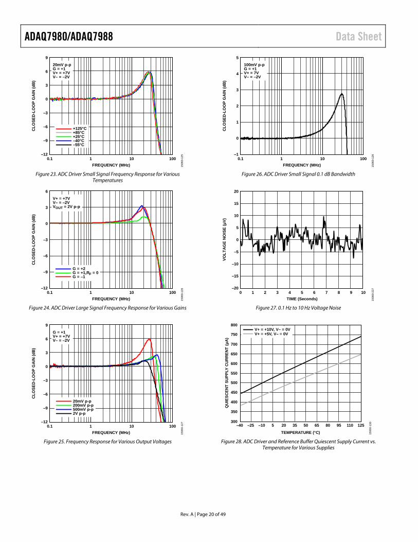
Rev. A | Page 20 of 49
9
–6
–9
3
6
0
–3
–12100101
CLO
SED
-LO
OP
GA
IN (d
B)
FREQUENCY (MHz)
20mV p-pG = +1V+ = +7VV– = –2V
+125°C+85°C+25°C–40°C–55°C
0.1
1506
0-12
5
Figure 23. ADC Driver Small Signal Frequency Response for Various
Temperatures
6
–6
–9
3
0
–3
–12100101
CLO
SED
-LO
OP
GA
IN (d
B)
FREQUENCY (MHz)
V+ = +7VV– = –2VVOUT = 2V p-p
G = +2G = +1,RF = 0G = –1
0.1
1506
0-12
6
Figure 24. ADC Driver Large Signal Frequency Response for Various Gains
9
–6
–9
3
6
0
–3
–120.1 100101
CLO
SED
-LO
OP
GA
IN (d
B)
FREQUENCY (MHz)
G = +1V+ = +7VV– = –2V
20mV p-p200mV p-p500mV p-p2V p-p
1506
0-12
7
Figure 25. Frequency Response for Various Output Voltages
5
1
0
4
3
2
–1100101
CLO
SED
-LO
OP
GA
IN (d
B)
FREQUENCY (MHz)
100mV p-pG = +1V+ = 7VV– = –2V
0.1
1506
0-12
8
Figure 26. ADC Driver Small Signal 0.1 dB Bandwidth
20
–5
–15
–10
10
15
5
0
–200 10987654321
VOLT
AG
E N
OIS
E (µ
V)
TIME (Seconds) 1506
0-22
7
Figure 27. 0.1 Hz to 10 Hz Voltage Noise
300
350
400
450
500
550
600
650
700
750
800
–40 –25 –10 5 20 35 50 65 80 95 110 125
QU
IESC
ENT
SUPP
LY C
UR
REN
T (µ
A)
TEMPERATURE (°C)
V+ = +5V, V– = 0VV+ = +10V, V– = 0V
1506
0-13
0
Figure 28. ADC Driver and Reference Buffer Quiescent Supply Current vs.
Temperature for Various Supplies

Data Sheet ADAQ7980/ADAQ7988
Rev. A | Page 21 of 49
0.6
0.5
0.4
0.3
0.2
0.1
00 10987654321
REC
OVE
RY
TIM
E (µ
s)
OVERLOAD DURATION (µs) 1506
0-22
9
G = +1V+ = +7VV– = –2VVIN = 10% OVERDRIVE
Figure 29. Recovery Time vs. Overload Duration
–180
–160
–140
–120
–100
–80
–60
–40
–20
0
–20
0
20
40
60
80
100
120
10 100 1k 10k 100k 1M 10M 100M
OPE
N-L
OO
P PH
ASE
(Deg
rees
)
OPE
N-L
OO
P G
AIN
(dB
)
FREQUENCY (Hz)
GAIN
PHASE
1506
0-13
2
Figure 30. ADC Driver Open-Loop Gain and Phase vs. Frequency
0
200
400
600
800
100
1200
1400
–55 –35 –15 5 25 45 65 85 105 125
ADC
DRIV
ERDY
NAM
IC P
OW
ER S
CALI
NG T
URN-
ON
TIM
E (n
s)
TEMPERATURE (°C) 1506
0-23
1
fS = 100kSPSV– = 0VVREF = 3.3V
V+ = 10VV+ = 7VV+ = 5V
Figure 31. ADC Driver Dynamic Power Scaling Turn-On Time vs. Temperature for Various Supply Voltages
1200
1000
800
600
400
200
04 1098765
AD
C D
RIV
ER D
YNA
MIC
PO
WER
SC
ALI
NG
TUR
N O
N T
IME
(ns)
SUPPLY (V) 1506
0-23
3
fS = 100kSPSV– = 0VVREF = 3.3V
Figure 32. ADC Driver Dynamic Power Scaling Turn On Time vs. Supply
Voltage
0
100
200
300
400
500
600
800
700
0 1 2 3 4 5 6
SUPP
LY C
URRE
NT (µ
A)
TIME (µs) 1506
0-24
2
V– = 0VV+ = 10VV+ = 5VV+ = 4V
Figure 33. Supply Current vs. ADC Driver and Reference Buffer Turn-Off
Response Time for Various Supplies
0
100
200
300
400
500
600
700
800
0 1 2 3 4 5 6
SUPP
LY C
URRE
NT (µ
A)
TIME (µs) 1506
0-23
5
V+ = 5VV– = 0V+125°C
+25°C–40°C
Figure 34. Supply Current vs. ADC Driver and Reference Buffer Turn-Off Response Time for Various Temperatures

ADAQ7980/ADAQ7988 Data Sheet
Rev. A | Page 22 of 49
–140
–120
–100
–80
–60
–40
–20
0
20
10 100 1k 10k 100k 1M 10M 100M
FREQUENCY (Hz)
+PSRR
CMRR
CM
RR
, PSR
R (d
B)
V+ = 5V, V– = 0VΔV+, ΔVCM = 100mV p-p
1506
0-13
8
Figure 35. CMRR and PSRR vs. Frequency
0.5
1.0
1.5
2.0
2.5
3.0
3.5
4.0
3.0 3.5 4.0 4.5 5.0 5.5 6.0 6.5 7.0 7.5 8.0 8.5 9.0 9.5 10.0
POW
ER-D
OW
N T
HR
ESH
OLD
(V)
SUPPLY VOLTAGE FROM GROUND (V)
DEVICE ENABLED
DEVICE DISABLED
TA = –40°CTA = +25°CTA = +125°C
1506
0-13
9
Figure 36. ADC Driver and Reference Buffer Power-Down Threshold vs. Supply Voltage from Ground for Various Temperatures
0.0025
0.0005
0.0020
0.0015
0.0010
0–55 12545–15 855 65 10525–35
GAI
N ER
ROR
(% F
S)
TEMPERATURE (°C) 1506
0-14
0
Figure 37. Gain Error vs. Temperature
90
–30
70
30
50
10
–10
–50–55 12545–15 855 65 10525–35
REFE
RENC
E BU
FFER
OFF
SET
VOLT
AGE
(µV)
TEMPERATURE (°C) 1506
0-14
1
Figure 38. Reference Buffer Input Offset Voltage vs. Temperature
1.5
0.7
1.4
1.2
1.3
1.1
0.9
0.6
1.0
0.8
0.5–55 12545–15 855 65 10525–35
SUPP
LY C
URRE
NT (m
A)
TEMPERATURE (°C)
fSAMPLE = 0Hz
V+ = 10VV+ = 5VV+ = 3.8V
1506
0-14
2
Figure 39. ADC Driver and Reference Buffer Static Supply Current vs. Temperature for Various Supplies
1.9
1.7
1.3
1.5
1.1
0.7
0.9
0.5–55 12545–15 855 65 10525–35
SUPP
LY C
URRE
NT (m
A)
TEMPERATURE (°C)
V+ = 10VV+ = 5VV+ = 3.8V
1506
0-14
3
Figure 40. ADC Driver and Reference Buffer Dynamic Supply Current vs.
Temperature for Various Supplies

Data Sheet ADAQ7980/ADAQ7988
Rev. A | Page 23 of 49
0.020
0.015
0.005
0.010
0–55 12545–15 855 65 10525–35
PD C
UR
REN
T (m
A)
TEMPERATURE (°C)
PD CURRENT 10V SUPPLY DELTAPD CURRENT 5V SUPPLY DELTAPD CURRENT 3.8V SUPPLY DELTA
fSAMPLE = 0Hz
1506
0-14
4
Figure 41. Total ADC Driver and Reference Buffer Power-Down (PD) Current vs. Temperature
0.05
0.03
–0.01
–0.03
0.01
–0.05–55 12545–15 855 65 10525–35
OFF
SET
ERR
OR
(mV)
TEMPERATURE (°C)
OFFSET ERROR V+ = +7V, V– = –2VOFFSET ERROR V+ = +5V, V– = 0V
1506
0-14
5
Figure 42. Offset Error vs. Temperature
1.6
1.4
0.8
0.4
1.2
0.6
0.2
1.0
0–55 12545–15 855 65 10525–35
LDO
CUR
RENT
(mA)
TEMPERATURE (°C)
LDO DYNAMIC CURRENT 10V INPUTLDO STATIC CURRENT 10V INPUT
1506
0-14
6
Figure 43. LDO Current vs. Temperature for Various Supplies
0
0.5
1.0
1.5
2.0
2.5
3.5
3.0
0 100k 200k 300k 400k 500k 600k 700k 800k 900k 1000k
TOTA
L O
PER
ATI
NG
CU
RR
ENT
(mA
)
SAMPLE RATE (SPS) 1506
0-24
5
V+ = 3.8V, V– = 0VV+ = 5V, V– = 0VV+ = 7.7V, V– = 0VV+ = 10V, V– = 0V
Figure 44. Total Operating Current vs. Sample Rate for Various Supplies
2.60
2.55
2.45
2.50
2.40–55 12545–15 855 65 10525–35
LDO
_OU
T (V
)
TEMPERATURE (°C) 1506
0-14
8
Figure 45. Output Voltage (LDO_OUT) vs. Temperature
2.55
2.53
2.49
2.47
2.51
2.450 1005020 7030 60 90804010
LDO
_OU
T (V
)
LOAD CURRENT (mA) 1506
0-14
9
Figure 46. Output Voltage (LDO_OUT) vs. Load Current (ILOAD)

ADAQ7980/ADAQ7988 Data Sheet
Rev. A | Page 24 of 49
2.45
2.55
2.53
2.51
2.49
2.47
4 5 6 7 8 9 10
LDO
_OUT
(V)
VDD (V) 1506
0-24
8
ILOAD = 1mAILOAD = 10mAILOAD = 100mA
Figure 47. Output Voltage (LDO_OUT) vs. VDD
–55 12545–15 855 65 10525–35TEMPERATURE (°C)
0.0020
0.0015
0.0005
0.0010
0
LDO
PD
CURR
ENT
(mA)
fSAMPLE = 0HzVDD = 5V
1506
0-15
1
Figure 48. LDO PD Current vs. Temperature
0
0.20
0.16
0.12
0.08
0.04
0.02
0.18
0.14
0.10
0.06
0.0001 0.001 0.01 0.1
LDO
DRO
POUT
VO
LTAG
E (V
)
ILOAD (mA) 1506
0-25
0
Figure 49. LDO Dropout Voltage vs. Load Current (ILOAD), LDO_OUT = 2.5 V
2.30
2.60
2.55
2.50
2.45
2.40
2.35
2.50 3.002.952.902.852.802.752.702.652.602.55
LDO
_OUT
(V)
VDD (V) 1506
0-25
1
ILOAD = 1mAILOAD = 10mAILOAD = 100mA
Figure 50. LDO_OUT vs. VDD in Dropout, LDO_OUT = 2.5 V
–90
–80
–70
–60
–50
–40
–30
–20
–10
0.01 0.1 1 10 100
ISO
LATI
ON
(dB)
FREQUENCY (MHz)
V+ = 5VV– = 0VVIN = 0.5 V p-p
1506
0-15
4
Figure 51. Forward/Off Isolation vs. Frequency

Data Sheet ADAQ7980/ADAQ7988
Rev. A | Page 25 of 49
TERMINOLOGY Integral Nonlinearity Error (INL) INL refers to the deviation of each individual code from a line drawn from negative full scale through positive full scale. The point used as negative full scale occurs ½ LSB before the first code transition. Positive full scale is a level 1½ LSB beyond the last code transition. The deviation is measured from the middle of each code to the true straight
Differential Nonlinearity Error (DNL) In an ideal ADC, code transitions are 1 LSB apart. DNL is the maximum deviation from this ideal value. It is often specified in terms of resolution for which no missing codes are guaranteed.
Zero Error The first transition occurs at a level ½ LSB above analog ground (38.1 µV for the 0 V to 5 V range). The offset error is the deviation of the actual transition from that point.
Gain Error The last transition (from 111 … 10 to 111 … 11) occurs for an analog voltage 1½ LSB below the nominal full scale (4.999886 V for the 0 V to 5 V range). The gain error is the deviation of the actual level of the last transition from the ideal level after the offset is adjusted out.
Spurious-Free Dynamic Range (SFDR) SFDR is the difference, in decibels (dB), between the rms amplitude of the input signal and the peak spurious signal.
Effective Number of Bits (ENOB) ENOB is a measurement of the resolution with a sine wave input. It is related to SINAD by the following formula:
ENOB = (SINADdB − 1.76)/6.02
ENOB is expressed in bits.
Noise Free Code Resolution Noise free code resolution is the number of bits beyond which it is impossible to distinctly resolve individual codes. Calculate it as follows:
Noise Free Code Resolution = log2(2N/Peak to Peak Noise)
Noise free code resolution is expressed in bits.
Total Harmonic Distortion (THD) THD is the ratio of the rms sum of the first five harmonic components to the rms value of a full-scale input signal and is expressed in decibels (dB).
Dynamic Range Dynamic range is the ratio of the rms value of the full scale to the total rms noise measured with the inputs shorted together. The value for dynamic range is expressed in decibels (dB). It is measured with a signal at −60 dBFS to include all noise sources and DNL artifacts.
Signal-to-Noise Ratio (SNR) SNR is the ratio of the rms value of the actual input signal to the rms sum of all other spectral components below the Nyquist frequency, excluding harmonics and dc. The value for SNR is expressed in decibels (dB).
Signal-to-Noise-and-Distortion (SINAD) Ratio SINAD is the ratio of the rms value of the actual input signal to the rms sum of all other spectral components below the Nyquist frequency, including harmonics but excluding dc. The value for SINAD is expressed in decibels (dB).
Aperture Delay Aperture delay is the measure of the acquisition performance. It is the time between the rising edge of the CNV input and when the input signal is held for a conversion.
Transient Response Transient response is the time required for the ADC to accurately acquire its input after a full-scale step function is applied.

ADAQ7980/ADAQ7988 Data Sheet
Rev. A | Page 26 of 49
THEORY OF OPERATION
COMP
SWITCHES CONTROL
OUTPUT CODE
CNV
CONTROLLOGIC
SW+LSB
SW–LSB
IN+
REF
GND
IN–
MSB
MSB
CC4C 2C16,384C32,768C
CC4C 2C16,384C32,768C
1506
0-05
5
Figure 52. ADC Simplified Schematic
CIRCUIT INFORMATION The ADAQ7980/ADAQ7988 system in package (SiP) is a fast, low power, precise data acquisition (DAQ) signal chain that uses a SAR architecture. The μModule data acquisition system contains a high bandwidth, analog-to-digital converter (ADC) driver, a low noise reference buffer, a low dropout regulator (LDO), and a 16-bit SAR ADC, along with critical passive components required to achieve optimal performance. All active components in the circuit are designed by Analog Devices, Inc.
The ADAQ7980/ADAQ7988 are capable of converting 1,000,000 samples per second (1 MSPS) and 500,000 samples per second (500 kSPS), respectively. The ADC powers down between conversions; therefore, power consumption scales with sample rate. The ADC driver and reference buffer are capable of dynamic power scaling, where the power consumption of these components scales with sample rate. When operating at 1 kSPS, for example, the ADAQ7980/ADAQ7988 consume 2.9 mW typically, ideal for battery-powered applications.
The ADAQ7980/ADAQ7988 offer a significant form factor reduction compared to traditional signal chains while still providing flexibility to adapt to a wide array of applications. All three signal pins of the ADC driver are available to the user, allowing various amplifier configurations. The devices house the LPF between the driver and the ADC, controlling the signal chain bandwidth and providing a bill of materials reduction. The ADAQ7980/ADAQ7988 do not exhibit any pipeline delay or latency, making them ideal for multiplexed applications.
The ADAQ7980/ADAQ7988 house a reference buffer and the corresponding decoupling capacitor. The placement of this decoupling capacitor is vital to achieving peak conversion performance. Inclusion of this capacitor in the μModule data acquisition system eliminates this performance hurdle. The reference buffer is configured for unity gain. By only including the reference buffer, the user has the flexibility to choose the reference buffer input voltage that matches the desired analog input range.
The ADAQ7980/ADAQ7988 interface to any 1.8 V to 5 V digital logic family. They are housed in a tiny 24-lead LGA that provides significant space savings and allows flexible configurations.
CONVERTER OPERATION The ADAQ7980/ADAQ7988 contain a successive approximation ADC based on a charge redistribution digital-to-analog converter (DAC). Figure 52 shows the simplified schematic of the ADC. The capacitive DAC consists of two identical arrays of 16 binary weighted capacitors, which are connected to the two comparator inputs.
During the acquisition phase, terminals of the array tied to the input of the comparator are connected to GND via the internal switches (SW+ and SW−). All independent switches are connected to the analog inputs. Therefore, the capacitor arrays are used as sampling capacitors and acquire the analog signal on the ADC inputs. When the acquisition phase is completed and the CNV input goes high, a conversion phase initiates. When the conversion phase begins, SW+ and SW− open first. The two capacitor arrays are then disconnected from the ADC input and connected to the GND input. Therefore, the differential voltage between the ADC input pins captured at the end of the acquisition phase are applied to the comparator inputs, causing the comparator to become unbalanced. By switching each element of the capacitor array between GND and REF, the comparator input varies by binary weighted voltage steps (VREF/2, VREF/4 … VREF/65,536). The control logic toggles these switches, starting with the MSB, to bring the comparator back into a balanced condition. After the completion of this process, the devices return to the acquisition phase, and the control logic generates the ADC output code and a busy signal indicator signaling the user that the conversion is complete.
Because the ADAQ7980/ADAQ7988 have an on-board conversion clock, the serial clock (SCK) is not required for the conversion process.

Data Sheet ADAQ7980/ADAQ7988
Rev. A | Page 27 of 49
Transfer Functions
The ideal transfer characteristics for the ADAQ7980/ADAQ7988 are shown in Figure 53 and Table 11.
000 ... 000
000 ... 001
000 ... 010
111 ... 101
111 ... 110
111 ... 111
–FSR –FSR + 1LSB
–FSR + 0.5LSB
+FSR – 1 LSB
+FSR – 1.5 LSB
ANALOG INPUT
AD
C C
OD
E (
ST
RA
IGH
T B
INA
RY
)
1506
0-05
6
Figure 53. ADC Ideal Transfer Function
Table 11. Output Codes and Ideal Input Voltages Analog Input1
Description VREF = 5 V Digital Output Code (Hex) FSR – 1 LSB 4.999924 V 0xFFFF2 Midscale + 1 LSB 2.500076 V 0x8001 Midscale 2.5 V 0x8000 Midscale – 1 LSB 2.499924 V 0x7FFF –FSR + 1 LSB 76.3 μV 0x0001 –FSR 0 V 0x00003
1 The ADAQ7980/ADAQ7988 ADC driver in the unity-gain buffer configuration. 2 This is also the code for an overranged analog input (IN+ − IN− above VREF − VGND). 3 This is also the code for an underranged analog input (IN+ − IN− below VGND).
TYPICAL CONNECTION DIAGRAM Figure 54 shows an example of the recommended connection diagram for the ADAQ7980/ADAQ7988 when multiple supplies are available.
REF
GND
VDD
VIO
SDI
SCK
SDO
CNV
20Ω
V+
V–
1.8nF
10µFLDO
2.2µF
REF_OUT LDO_OUT
PD_REF2
AMP_OUT
PD_AMP2
NEGATIVESUPPLY
POSITIVESUPPLY
REF1
PD_LDO2
ADC
ADCN
IN+
IN–
1.8V TO 5V
100nF
100nF
100nF 2.2µF
0V TOVREF
1SEE THE VOLTAGE REFERENCE INPUT SECTION FOR REFERENCE SELECTION.2POWER DOWN PINS CONNECTED TO EITHER DIGITAL HOST OR POSITIVE SUPPLY. 15
060-
057
Figure 54. Typical Application Diagram with Multiple Supplies

ADAQ7980/ADAQ7988 Data Sheet
Rev. A | Page 28 of 49
ADC DRIVER INPUT The ADC driver of the ADAQ7980/ADAQ7988 features a −3 dB bandwidth of 35 MHz and a slew rate of 110 V/μs at G = +1 and VAMP_OUT = 2 V step. It features an input voltage noise of 5.9 nV/√Hz .The driver can operate over a supply voltage range of 3.8 V to 10 V and consumes only 500 μA of supply current at a supply difference of 5 V. The low end of the supply range allows −5% variation of a 4 V supply. The amplifier is unity-gain stable, and the input structure results in an extremely low input voltage noise 1/f corner. The ADC driver uses a slew enhancement architecture, as shown in Figure 55. The slew enhancement circuit detects the absolute difference between the two inputs. It then modulates the tail current, ITAIL, of the input stage to boost the slew rate. The architecture allows a higher slew rate and a faster settling time with a low quiescent current while maintaining low noise. The user has access to all three amplifier signal pins, providing flexibility to adapt to the desired application or configuration.
IN+
VIN+ VIN–
V+
INPUTSTAGE
TO DETECTABSOLUTE
VALUE
SLEW ENHANCEMENT CIRCUIT
ITAIL
IN–
1506
0-05
8
Figure 55. ADC Driver Slew Enhancement Circuit
INPUT PROTECTION The amplifier is fully protected from ESD events, withstanding human body model ESD events of 4000 V and field induced charged device model events of 1250 V with no measured performance degradation. The precision input is protected with an ESD network between the power supplies and diode clamps across the input device pair, as shown in Figure 56.
IN+
ESD
ESD
V–
V+
BIAS
TO THE REST OF THE AMPLIFIER
IN–
ESD
ESD
1506
0-05
9
Figure 56. ADC Driver Input Stage and Protection Diodes
For differential voltages more than approximately 1.2 V at room temperature and 0.8 V at 125°C, the diode clamps begin to conduct. If large differential voltages must be sustained across the input terminals, the current through the input clamps must be limited to less than 10 mA.
External series input resistors that are sized appropriately for the expected differential overvoltage can provide the needed protection.
The ESD clamps begin to conduct for input voltages that are more than 0.7 V above the positive supply and input voltages more than 0.7 V below the negative supply. If an overvoltage condition is expected, the input current must be limited to less than 10 mA.
Along with the ADC driver inputs, protection is also provided on the ADC input. As shown in Figure 1, the ADAQ7980/ADAQ7988 house an RC filter between the ADC driver and the ADC. The series resistor in this low-pass filter acts to limit current in an overvoltage condition. The current sink capability of the reference buffer works to hold the reference node at its desired value when the ADC input protection diodes conduct due to an overvoltage event.
Figure 57 shows an equivalent ADC analog input circuit of the ADAQ7980/ADAQ7988.
The two diodes, D1 and D2, provide ESD protection for the ADC inputs. Take care to ensure that the ADC analog input signal never exceeds the reference value by more than 0.3 V or drops below ground by more than 0.3 V because this causes diodes to become forward-biased and start conducting current. These diodes can handle a forward-biased current greater than or equal to the short-circuit current of the ADC driver. For instance, these conditions can occur when the ADC driver positive supply is greater than the reference value. In such a case (for example, an input buffer with a short circuit), use the current limitation to protect the devices.
REF
RINCIN
IN+OR IN–
GND
D2CPIN
D1
1506
0-06
0
Figure 57. Equivalent ADC Analog Input Circuit
The analog input structure allows the sampling of the true differential signal between the ADC input pins. By using these differential inputs, signals common to both inputs are rejected.
NOISE CONSIDERATIONS AND SIGNAL SETTLING The ADC driver of the ADAQ7980/ADAQ7988 is ideal for driving the on-board high resolution SAR ADC. The low input voltage noise and rail-to-rail output stage of the driver helps to minimize distortion at large output levels. With its low power of 500 μA, the amplifier consumes power that is compatible with the low power SAR ADC. Furthermore, the ADC driver supports a single-supply configuration; the input common-mode range extends to the negative supply, and 1.3 V below the positive supply.

Data Sheet ADAQ7980/ADAQ7988
Rev. A | Page 29 of 49
Figure 58 illustrates the primary noise contributors for the typical gain configurations. The total output noise (vn_out) is the root sum square of all the noise contributions.
RG
RS
in–
RF
vn
4kTRSvn_RS =
4kTRGvn_RG =
vn_RF =
+ vn_out –
4kTRF
in+
1506
0-06
1
Figure 58. Noise Sources in Typical Connection
Calculate the output noise spectral density of the ADC driver by
[ ] 22
2
222
2
_
4414 FnGG
FnSn
G
FF
outn
RikTRRRvRikTRs
RRkTR
v
−+ +
+++
++
=
where: k is the Boltzmann constant. T is the absolute temperature in degrees Kelvin. RF and RG are the feedback network resistances, as shown in Figure 58. RS is the source resistance, as shown in Figure 58. in+ and in− represent the amplifier input current noise spectral density in pA/√Hz. vn is the amplifier input voltage noise spectral density in nV/√Hz.
For more information on these calculations, see MT-049 and MT-050.
Source resistance noise, amplifier input voltage noise (vn), and the voltage noise from the amplifier input current noise (in+ × RS) are all subject to the noise gain term (1 + RF/RG).
Figure 59 shows the total referred to input (RTI) noise due to the amplifier vs. the source resistance. Note that with a 5.9 nV/√Hz input voltage noise and 0.6 pA/√Hz input current noise, the noise contributions of the amplifier are relatively small for source resistances from approximately 2.6 kΩ to 47 kΩ.
The Analog Devices, Inc., silicon germanium (SiGe) bipolar process makes it possible to achieve a low voltage noise. This noise is much improved compared to similar low power amplifiers with a supply current in the range of hundreds of microamperes.
1
10
100
1k
100 1k 10k 100k 1M
RTI
NO
ISE
(nV/
√Hz)
SOURCE RESISTANCE (Ω)
TOTAL NOISESOURCE RESISTANCE NOISEAMPLIFIER NOISE
SOURCE RESISTANCE = 2.6kΩ
SOURCE RESISTANCE = 47kΩ
1506
0-06
2
Figure 59. RTI Noise vs. Source Resistance
Keep the noise generated by the driver amplifier, and its associated passive components, as low as possible to preserve the SNR and transition noise performance of the ADAQ7980/ ADAQ7988. The analog input circuit of the ADAQ7980/ ADAQ7988 features a one-pole, low-pass filter to band limit the noise coming from the ADC driver. Because the typical noise of the ADAQ7980/ADAQ7988 is 44.4 µV rms in the dual-supply typical configuration, the SNR degradation due to the amplifier is
+=
−2
dB32 )(
2π44.4
44.4log20
N
LOSS
NefSNR
where: f–3 dB is the cutoff frequency of the input filter (4.4 MHz). N is the noise gain of the amplifier (for example, 1 in a buffer configuration). eN is the equivalent input noise voltage of the op amp, in nV/√Hz.
For multichannel multiplexed applications, the analog input circuit of the ADAQ7980/ADAQ7988 must settle a full-scale step onto the capacitor array at a 16-bit level (0.0015%, 15 ppm) within one conversion period. As shown in Figure 20, the bandwidth of the ADC driver changes with the gain setting implemented. The ADC driver must maintain a sufficient bandwidth to allow the ADC input to settle properly. The RC time constant of the low-pass filter of the ADAQ7980/ADAQ7988 has been set to settle the anticipated SAR ADC charge redistribution voltage step from a full-scale ADC input voltage transition within the minimum acquisition phase of the ADC. The maximum full-scale step is based upon the maximum reference input voltage of 5.1 V. The reference sets the maximum analog input range and subsequently the range of voltages that the ADC can quantize.

ADAQ7980/ADAQ7988 Data Sheet
Rev. A | Page 30 of 49
During the conversion process, the capacitive DAC of the SAR ADC disconnects from the ADC input. In a multiplexed application, the multiplexer input channel switches during the conversion time to provide the maximum settling time. At the end of the conversion time, the capacitive DAC then connects back to the input. During this time, the DAC is disconnected from the ADC input, and a voltage change occurs at the ADC input node. The voltage step observed at the ADC analog input resulting from capacitive charge redistribution attenuates due to the voltage divider created by the parallel combination of the capacitive DAC and the capacitor in the external low-pass filter. Calculate the voltage step by
VSTEP = (VREF × 30 pF)/(30 pF + 1800 pF) = VREF × 0.016
For a 5.0 V reference, this results in a maximum step size of 82 mV. To calculate the required filter and ADC driver bandwidth, determine the number of time constants required to settle this voltage step within the ADC acquisition phase as follows:
=
+1162
lnREF
STEPTC V
VN
With the number of time constants known, determine the RC time constant (τ) by τ = 290 ns/NTC. The minimum acquisition phase of the ADC is 290 ns. Signals must be fully settled within this acquisition period.
Calculate the filter bandwidth (BW) by BW = 1/(2π × τ).
The ADC driver small signal bandwidth must always remain greater than or equal to the bandwidth previously calculated. When the small signal bandwidth reduces, for example in the presence of a large voltage gain, increase the acquisition phase to increase the required system τ. An increase in acquisition phase results in a reduction of the maximum sample rate.
The method previously described assumes the multiplexer switches shortly after the conversion begins and that the amplifier and RC have a large enough bandwidth to sufficiently settle the low-pass filter capacitor before acquisition begins.
During forward settling, approximately 11 time constants are required to settle a full-scale step to 16 bits. For the low-pass RC filter housed in the ADAQ7980/ADAQ7988, the forward settling time of the filter is 11 × 36 ns ≈ 400 ns, which is much less than the conversion time of 710 ns/1200 ns, respectively. To achieve an ADC driver forward settling time of less than 710 ns, maintain an ADC driver large signal bandwidth of 2.49 MHz. Calculate this as follows:
ADC Driver Forward Settling Time Constant = 710 ns/ln(216) = 64 ns
Minimum ADC Driver Large Signal Bandwidth = 1/(2 π × 64 ns) = 2.49 MHz
The forward settling does not necessarily have to occur during the conversion time (before the capacitive DAC gets switched to the input), but the combined forward and reverse settling time must not exceed the required throughput rate. Forward settling is less important for low frequency inputs because the rate of change of the signal is much lower. The importance of which bandwidth specification of the ADC driver is used is dependent upon the type of input. Focus high frequency (>100 kHz) or multiplexed applications on the large signal bandwidth, and concentrate lower input frequency applications on the ADC driver small signal bandwidth when performing the previous calculations.
CONVERSION
MUX CHANNEL SWITCH
CNV
ADC THROUGHPUT tCYC
tCONV tACQ
ACQUISITIONACQUISITION
ADC INPUT
NEGATIVE FS
POSITIVE FS
REVERSESETTLING
CAPACITIVE DAC SWITCH TO ACQUIRE
FORWARDSETTLING
1506
0-06
3
Figure 60. Multiplexed Application Timing

Data Sheet ADAQ7980/ADAQ7988
Rev. A | Page 31 of 49
PD_AMP OPERATION
Figure 61 shows the ADC driver and reference buffer shutdown circuitry. To maintain a low supply current in shutdown mode, no internal pull-up circuitry exists; therefore, drive the PD_AMP pin high or low externally and do not leave it floating. Pulling the PD_AMP pin to ≥1 V below midsupply turns the device off, reducing the supply current to 2.9 µA for a 5 V supply. When the amplifier powers down, its output enters a high impedance state. The output impedance decreases as frequency increases. In shutdown mode, a forward isolation of −62 dB can be achieved at 100 kHz (see Figure 51).
V+
V–
PD_AMP
ESD
ESD
2.2Ω
1.8Ω
1.1V
TO ENABLEAMPLIFIER
1506
0-07
3
Figure 61. Shutdown Circuit
ESD clamps protect the PD_AMP pin, as shown in Figure 61. Voltages beyond the power supplies cause these diodes to conduct. To protect the PD_AMP pin, ensure that the voltage to this pin does not exceed 0.7 V above the positive supply or 0.7 V below the negative supply. If expecting an overvoltage condition, limit the input current to less than 10 mA with a series resistor.
Table 12 summarizes the threshold voltages for the powered down and enabled modes for various supplies. For any supply voltage, pulling the PD_AMP pin to ≥1 V below midsupply turns the device off.
Table 12. Threshold Voltages for Powered Down and Enabled Modes
Mode V+/V−
+4 V/0 V +5 V/0 V +7 V/−2 V Enabled >+1.4 V >+1.9 V >+1.9 V Powered Down <+1.0 V <+1.5 V <+1.5 V
DYNAMIC POWER SCALING (DPS) One of the merits of a SAR ADC is that its power scales with the sampling rate. This power scaling makes SAR ADCs very power efficient, especially when running at lower sampling frequencies. Traditionally, the ADC driver associated with the SAR ADC consumes constant power, regardless of the sampling frequency. The ADC driver allows dynamic power scaling. This feature allows the user to provide a periodic signal to the power-down pin of the ADC driver that is synchronized to the convert start signal, thus scaling the system power consumption with the sample rate.
Figure 62 illustrates the method by which the sampling rate of the system dynamically scales the quiescent power of the ADC driver. By providing properly timed signals to the convert start (CNV) pin of the ADC and the PD_AMP pins of the ADC driver, both devices run at optimum efficiency.
REF
GND
VDD
VIOSDISCKSDO
CNV
20Ω
V+
V–
1.8nF
10µFLDO
2.2µF
REF_OUT LDO_OUT
PD_REF
AMP_OUT
PD_AMP
PD_LDO
ADC
ADCN
IN+
IN–
ADAQ7980/ADAQ7988
TIMINGGENERATOR 15
060-
065
Figure 62. Power Management Circuitry
Figure 63 illustrates the relative signal timing for power scaling the ADC driver and the ADC. To prevent degradation in the performance of the ADC, the ADC driver must have a fully settled output into the ADC before the activation of the CNV pin. In this example, the amplifier is switched to full power mode 3 µs prior to the rising edge of the CNV signal. The PD_AMP pin of the ADC driver is pulled low when the ADC input is inactive in between samples. The quiescent current of the amplifier typically falls to 10% of the normal operating value within 0.9 µs at a supply difference of 5 V. While in shutdown mode, the ADC driver output impedance is high.

ADAQ7980/ADAQ7988 Data Sheet
Rev. A | Page 32 of 49
SAMPLING FREQUENCY = 100kHztS = 10µs
ACQUISITION ACQUISITION ACQUISITION
SHUTDOWN
3µs 3µs
POWEREDON
POWEREDON
POWEREDON SHUTDOWN SHUTDOWN
Vf1
tf1tTURNOFF1 tf2
Vf2
tTURNOFF2
tAMP, ON
Vf3
tf3tTURNOFF3
ADCMODE
CNV
PD_AMP
CONVERSION CONVERSION CONVERSION
MINIMUMPOWERED ON TIME = 3µs
ADC DRIVEROUTPUT
1506
0-06
6
Figure 63. Timing Waveforms
Figure 64 shows the quiescent power of the ADC driver with and without the power scaling. Without power scaling, the amplifier constantly consumes power regardless of the sampling frequency, as shown in the following equation.
PQ = IQ × VS
With power scaling, the quiescent power becomes proportional to the ratio of the amplifier on time (tAMP, ON) and the sampling time (tS).
PQ = IQ × VS × (tAMP, ON/tS)
Thus, by dynamically switching the driver between shutdown and full power modes during the sample period, the quiescent power of the driver scales with the sampling rate.
1.2
1.0
0.4
0.8
0.2
0.6
01 1M100k100 1k 10k10
QUI
ESCE
NT C
URRE
NT (m
A)
SAMPLING FREQUENCY (fS)
AMP QUIESCENT CURRENT NO DPSAMP QUIESCENT CURRENT WITH DPSADC CURRENT DRAW
PD_AMP ONTIME = 3µsV+ = 5VV– = 0V
1506
0-06
7
Figure 64. Quiescent Current of the ADC Driver vs. ADC Sampling Frequency

Data Sheet ADAQ7980/ADAQ7988
Rev. A | Page 33 of 49
SLEW ENHANCEMENT The ADC driver has an internal slew enhancement circuit that increases the slew rate as the feedback error voltage increases. This circuit improves the amplifier settling response for a large step, as shown in Figure 65. This improvement in settling response is useful in applications where the multiplexing of multiple input signals occurs.
–0.5
2.5
2.0
1.5
1.0
0.5
0
0 20 40 60 80 100 120 140
OU
TP
UT
VO
LT
AG
E (
V)
TIME (ns) 1506
0-26
6
500mV p-p1V p-p2V p-p
Figure 65. Step Response with Selected Output Steps
EFFECT OF FEEDBACK RESISTOR ON FREQUENCY RESPONSE The amplifiers input capacitance and feedback resistor form a pole that, for larger value feedback resistors, can reduce phase margin and contribute to peaking in the frequency response. Figure 66 shows the peaking for 500 Ω feedback resistors (RF) when the amplifier is configured in a gain of +2. Figure 66 also shows how peaking can mitigate with the addition of a small value capacitor placed across the feedback resistor of the amplifier.
–6
9
6
3
0
–3
0.1 1 10 100
CL
OS
ED
-LO
OP
GA
IN (
dB
)
FREQUENCY (MHz) 1506
0-26
7
8pF0pFG = +2
RF, RG = 500ΩVOUT = 200mV p-p
Figure 66. Peaking Mitigation in Small Signal Frequency Response
VOLTAGE REFERENCE INPUT The ADAQ7980/ADAQ7988 voltage reference input (REF) is the noninverting node of the on-board low noise reference buffer. The reference buffer is included to optimally drive the dynamic input impedance of the SAR ADC reference node. Also housed in the ADAQ7980/ADAQ7988 is a 10 μF decoupling capacitor that is ideally laid out within the devices. This decoupling capacitor is a required piece of the SAR architecture. The REF_OUT capacitor is not just a bypass capacitor. This capacitor is part of the SAR ADC that simply cannot fit on the silicon.
During the bit decision process, because the bits are settled in a few 10s of nanoseconds or faster, the storage capacitor replenishes the charge of the internal capacitive DAC. As the binary bit weighted conversion is processed, small chunks of charge are taken from the 10 μF capacitor. The internal capacitor array is a fraction of the size of the decoupling capacitor, but this large value storage capacitor is required to meet the SAR bit decision settling time.
There is no need for an additional lower value ceramic decoupling capacitor (for example, 100 nF) between the REF_OUT and GND pins.
The reference value sets the maximum ADC input voltage that the SAR capacitor array can quantize. The reference buffer is set in the unity-gain configuration; therefore, the user sets the reference voltage value with the REF pin and observes this value at the REF_OUT pin. The user is responsible for selecting a reference voltage value that is appropriate for the system under design. Allowable reference values range from 2.4 V to 5.1 V; however, do not violate the input common-mode voltage range specification of the reference buffer.
With the inclusion of the reference buffer, the user can implement a much lower power reference source than many traditional SAR ADC signal chains because the reference source drives a high impedance node instead of the dynamic load of the SAR capacitor array. Root sum square the reference buffer noise with the reference source noise to arrive at a total noise estimate. Generally, the reference buffer has a noise density much less than that of the reference source.
ADC
RG
BUFFER
VOLTAGEREFERENCE
OPTIONALFILTER
ADAQ7980
1506
0-07
2
Figure 67. Voltage Reference with RC Filtering
As shown in Figure 67, place a passive, RC low-pass filter with a very low cutoff frequency between the reference source and the REF pin of the ADAQ7980/ADAQ7988 to band limit noise from the reference source.

ADAQ7980/ADAQ7988 Data Sheet
Rev. A | Page 34 of 49
This filtering can be useful, considering the voltage reference source is usually the dominant contributor to the noise of the reference input circuit. Filters with extremely low bandwidths can be used since the reference signal is a dc type signal. However, because with such low frequency cutoffs, the settling time at power on is quite large. For example, a single pole, low-pass filter with a −3 dB bandwidth of 20 Hz has a time constant of approximately 8 ms.
Just like the ADC driver, the reference buffer features a PD_REF pin that allows the user to control the power consumption of the ADAQ7980/ADAQ7988. A timing scheme similar to Figure 63 can be implemented for the PD_REF pin. Also, use the PD_REF feature during long idle periods where extremely low power consumption is desired.
Figure 68 shows the reference buffer shutdown circuitry. To maintain very low supply current in shutdown mode, do not supply the internal pull-up resistor; therefore, the drive PD_REF pin high or low externally and do not leave it floating. Pulling the PD_REF pin to ≥1 V below midsupply turns the device off, reducing the supply current to 2.9 μA for a 5 V supply. When the amplifier powers down, its output enters a high impedance state. The output impedance decreases as frequency increases. In shutdown mode, a forward isolation of −80 dB can be achieved at frequencies below 10 kHz (see Figure 51).
V+
V–
PD_REF
ESD
ESD
2.2Ω
1.8Ω
1.1V
TO ENABLEAMPLIFIER
1506
0-06
4
Figure 68. Reference Buffer Shutdown Circuit
ESD clamps protect the PD_REF pin, as shown in Figure 68. Voltages beyond the power supplies cause these diodes to conduct. To protect the PD_REF pin, ensure that the voltage to this pin does not exceed 0.7 V above the positive supply or 0.7 V below the negative supply. When expecting an overvoltage condition, limit the input current to less than 10 mA with a series resistor. Table 13 summarizes the threshold voltages for the powered down and enabled modes for various supplies. For any supply voltage, pulling the PD_REF pin to ≥1 V below midsupply turns the device off.
Table 13. Threshold Voltages for Powered Down and Enabled Modes
Mode V+/V−
+4 V/0 V +5 V/0 V +7 V/−2 V Enabled >+1.4 V >+1.9 V >+1.9 V Powered Down <+1.0 V <+1.5 V <+1.5 V
If more than one ADAQ7980/ADAQ7988 is used in a system, for example, in a daisy-chain configuration, it is possible to use the reference buffer of one ADAQ7980/ADAQ7988 to provide the REF_OUT signal for multiple ADAQ7980/ADAQ7988 devices. Enabling the PD_REF pin of the reference buffer places the reference buffer output in a high impedance state. The active reference buffer can drive the subsequent REF_OUT nodes. See Figure 69 for connection details.
The sample rate of each individual converter determines the number of ADAQ7980/ADAQ7988 references that can be chained together. Each ADAQ7980/ADAQ7988 SAR ADC reference consumes 330 μA of load current at a reference input of 5 V and with the converter running at 1 MSPS. This current consumption scales linearly with sample rate. For example, reducing the sample rate to 100 kSPS reduces the reference current draw to 33 μA. The active reference buffer must regulate the cumulative current draw well enough so that the reference voltage does not change by more than ½ of an LSB. An unperceived change in reference value manifests as a gain error.
ADC
RG
BUFFER
VOLTAGEREFERENCE
OPTIONALFILTER
ADAQ7980/ADAQ7988
DEVICE 1
ADAQ7980/ADAQ7988
DEVICE 2
ADC
RG
BUFFER
ADAQ7980/ADAQ7988
DEVICE 3
ADC
RG
BUFFER
PD_REF 1 PD_REF 2 PD_REF 3 POWEREDOFF
POWEREDOFF
POWEREDON
1506
0-07
4
Figure 69. Reference Configuration for Multiple ADAQ7980/ADAQ7988 Devices
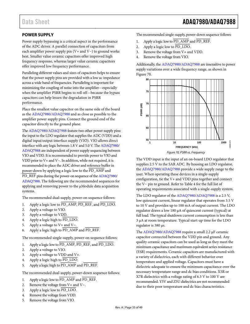
Data Sheet ADAQ7980/ADAQ7988
Rev. A | Page 35 of 49
POWER SUPPLY Power supply bypassing is a critical aspect in the performance of the ADC driver. A parallel connection of capacitors from each amplifier power supply pin (V+ and V−) to ground works best. Smaller value ceramic capacitors offer improved high frequency response, whereas larger value ceramic capacitors offer improved low frequency performance.
Paralleling different values and sizes of capacitors helps to ensure that the power supply pins are provided with a low ac impedance across a wide band of frequencies. Parralleling is important for minimizing the coupling of noise into the amplifier—especially when the amplifier PSRR begins to roll off—because the bypass capacitors can help lessen the degradation in PSRR performance.
Place the smallest value capacitor on the same side of the board as the ADAQ7980/ADAQ7988 and as close as possible to the amplifier power supply pins. Connect the ground end of the capacitor directly to the ground plane.
The ADAQ7980/ADAQ7988 feature two other power supply pins: the input to the LDO regulator that supplies the ADC (VDD) and a digital input/output interface supply (VIO). VIO allows direct interface with any logic between 1.8 V and 5.0 V. The ADAQ7980/ ADAQ7988 are independent of power supply sequencing between VIO and VDD. It is recommended to provide power to VIO and VDD prior to V+ and V−. In addition, while not required, it is recommended to place the ADC driver and reference buffer in power-down by applying a logic low to the PD_AMP and PD_REF pins during the power-on sequence of the ADAQ7980/ ADAQ7988. The following are the recommended sequences for applying and removing power to the μModule data acquisition systems.
The recommended dual-supply, power-on sequence follows:
1. Apply a logic low to PD_AMP, PD_REF, and PD_LDO. 2. Apply a voltage to VIO. 3. Apply a voltage to VDD. 4. Apply a logic high to PD_LDO. 5. Apply a voltage to V+ and V−. 6. Apply a logic high to PD_AMP and PD_REF.
The recommended single-supply, power-on sequence follows:
1. Apply a logic low to PD_AMP, PD_REF, and PD_LDO. 2. Apply a voltage to VIO. 3. Apply a voltage to VDD and V+. 4. Apply a logic high to PD_LDO. 5. Apply a logic high to PD_AMP and PD_REF.
The recommended dual-supply, power-down sequence follows:
1. Apply a logic low to PD_AMP and PD_REF. 2. Remove the voltage from V+ and V−. 3. Apply a logic low to PD_LDO. 4. Remove the voltage from VDD. 5. Remove the voltage from VIO.
The recommended single-supply, power-down sequence follows:
1. Apply a logic low to PD_AMP and PD_REF. 2. Apply a logic low to PD_LDO. 3. Remove the voltage from V+ and VDD. 4. Remove the voltage from VIO.
Additionally, the ADAQ7980/ADAQ7988 are insensitive to power supply variations over a wide frequency range, as shown in Figure 70.
80
551 1000
FREQUENCY (kHz)
PSR
R (d
B)
10 100
75
70
65
60
1506
0-07
5
Figure 70. PSRR vs. Frequency
The VDD input is the input of an on-board LDO regulator that supplies 2.5 V to the SAR ADC. By housing an LDO regulator, the ADAQ7980/ADAQ7988 provide a wide supply range to the user. When operating these devices in a single-supply configuration, tie the V+ and VDD pins together and connect the V− pin to ground. Refer to Table 4 for the full list of operating requirements associated with a single-supply system.
The LDO regulator of the ADAQ7980/ADAQ7988 is a 2.5 V, low quiescent current, linear regulator that operates from 3.5 V to 10 V and provides up to 100 mA of output current. The LDO regulator draws a low 180 µA of quiescent current (typical) at full load. The typical shutdown current consumption is less than 3 µA at room temperature. Typical start-up time for the LDO regulator is 380 µs.
The ADAQ7980/ADAQ7988 require a small 2.2 µF ceramic capacitor connected between the VDD pin and ground. Any quality ceramic capacitors can be used as long as they meet the minimum capacitance and maximum equivalent series resistance (ESR) requirements. Ceramic capacitors are manufactured with a variety of dielectrics, each with different behavior over temperature and applied voltage. Capacitors must have a dielectric adequate to ensure the minimum capacitance over the necessary temperature range and dc bias conditions. X5R or X7R dielectrics with a voltage rating of 6.3 V to 100 V are recommended. Y5V and Z5U dielectrics are not recommended due to their poor temperature and dc bias characteristics.

ADAQ7980/ADAQ7988 Data Sheet
Rev. A | Page 36 of 49
Internally, the LDO regulator consists of a reference, an error amplifier, a feedback voltage divider, and a positive metal-oxide semiconductor (PMOS) pass transistor. The PMOS pass device, which is controlled by the error amplifier, delivers the output current. The error amplifier compares the reference voltage with the feedback voltage from the output and amplifies the difference. If the feedback voltage is lower than the reference voltage, the gate of the PMOS device pulls lower, allowing more current to pass and increasing the output voltage. If the feedback voltage is higher than the reference voltage, the gate of the PMOS device pulls higher, allowing less current to pass and decreasing the output voltage.
The LDO regulator uses the PD_LDO pin to enable and disable the LDO_OUT pin under normal operating conditions. When PD_LDO is high, LDO_OUT turns on, and when PD_LDO is low, LDO_OUT turns off. For automatic startup, tie PD_LDO to VDD. Only apply a logic low to PD_LDO if a logic low is applied to PD_AMP and PD_REF as well.
LDO REGULATOR CURRENT-LIMIT AND THERMAL OVERLOAD PROTECTION The current and thermal overload protection circuits protect the LDO regulator of the ADAQ7980/ADAQ7988 against damage due to excessive power dissipation. The LDO regulator current limits when the output load reaches 360 mA (typical). When the output load exceeds the current limit threshold, the output voltage reduces to maintain a constant current limit.
Thermal overload protection is included, which limits the LDO regulator junction temperature to a maximum of 150°C (typical). Under extreme conditions (that is, high ambient temperature and/or high power dissipation), when the junction temperature starts to rise above 150°C, the output turns off, reducing the output current to zero. When the junction temperature drops below 135°C, the output turns on again, and the output current restores to its operating value.
Consider the case where a hard short circuit from LDO_OUT to ground occurs. At first, the LDO regulator limits the current threshold that can be conducted into the short circuit. If self heating of the junction is enough to cause its temperature to rise above 150°C, thermal shutdown activates, turning off the output and reducing the output current to zero. As the junction temperature cools and drops below 135°C, the output turns on and conducts the current limit into the short, again causing the junction temperature to rise above 150°C. This thermal oscillation between 135°C and 150°C causes a current oscillation between the maximum current and 0 mA that continues as long as the short circuit remains at the output.
Current-limit and thermal limit protections protect the device against accidental overload conditions. For reliable operation, externally limit the power dissipation of the devices so that the junction temperature does not exceed 125°C.
LDO REGULATOR THERMAL CONSIDERATIONS In applications with a low, input to output voltage differential, the LDO regulator does not dissipate much heat. However, in applications with high ambient temperature and/or high input voltage, the heat dissipated in the package may become large enough to cause the junction temperature of the die to exceed the specified junction temperature of 125°C.
When the junction temperature exceeds 150°C, the LDO regulator enters thermal shutdown. It recovers only after the junction temperature decreases below 135°C to prevent any permanent damage. Therefore, thermal analysis for the chosen application is important to guarantee reliable performance over all conditions. To guarantee specified operation, the junction temperature of the LDO regulator must not exceed 125°C. To ensure that the junction temperature stays below this value, the user must be aware of the parameters that contribute to junction temperature changes. These parameters include ambient temperature, power dissipation in the power device, and thermal resistances between the junction and ambient air (θJA). The θJA number is dependent on the package assembly compounds used and the amount of material used to solder the package GND pins to the PCB.

Data Sheet ADAQ7980/ADAQ7988
Rev. A | Page 37 of 49
DIGITAL INTERFACE Though the ADAQ7980/ADAQ7988 have a reduced number of pins, they offer flexibility in their serial interface modes.
The ADAQ7980/ADAQ7988, when in CS mode, are compatible with SPI, QSPI™, and digital hosts. This interface can use either a 3-wire or 4-wire interface. A 3-wire interface using the CNV, SCK, and SDO signals minimizes wiring connections useful, for instance, in isolated applications. A 4-wire interface using the SDI, CNV, SCK, and SDO signals allows CNV, which initiates the conversions, to be independent of the readback timing (SDI). This independence is useful in low jitter sampling or simultaneous sampling applications.
The ADAQ7980/ADAQ7988, when in chain mode, provide a daisy-chain feature using the SDI input for cascading multiple ADCs on a single data line similar to a shift register.
The mode in which these devices operate depends on the SDI level when the CNV rising edge occurs. To select CS mode, set SDI high, and to select chain mode, set SDI low. The SDI hold time is such that when SDI and CNV are connected together, chain mode is selected.
In either mode, the ADAQ7980/ADAQ7988 offer the flexibility to optionally force a start bit in front of the data bits. This start bit can be used as a busy signal indicator to interrupt the digital host and trigger the data reading. Otherwise, without a busy indicator, the user must time out the maximum conversion time prior to readback.
The busy indicator enables
• In CS mode if CNV or SDI is low when the ADC conversion ends (see Figure 74 and Figure 78).
• In chain mode if SCK is high during the CNV rising edge (see Figure 82).
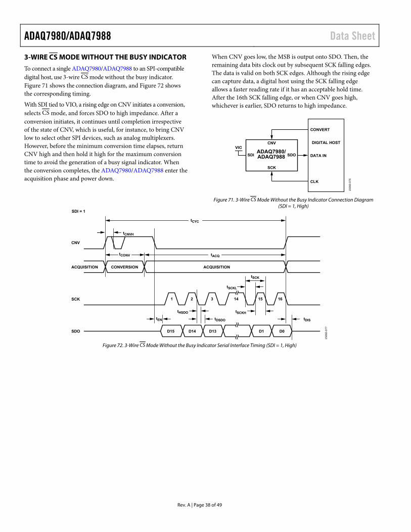
ADAQ7980/ADAQ7988 Data Sheet
Rev. A | Page 38 of 49
3-WIRE CS MODE WITHOUT THE BUSY INDICATOR
To connect a single ADAQ7980/ADAQ7988 to an SPI-compatible digital host, use 3-wire CS mode without the busy indicator. Figure 71 shows the connection diagram, and Figure 72 shows the corresponding timing.
With SDI tied to VIO, a rising edge on CNV initiates a conversion, selects CS mode, and forces SDO to high impedance. After a conversion initiates, it continues until completion irrespective of the state of CNV, which is useful, for instance, to bring CNV low to select other SPI devices, such as analog multiplexers. However, before the minimum conversion time elapses, return CNV high and then hold it high for the maximum conversion time to avoid the generation of a busy signal indicator. When the conversion completes, the ADAQ7980/ADAQ7988 enter the acquisition phase and power down.
When CNV goes low, the MSB is output onto SDO. Then, the remaining data bits clock out by subsequent SCK falling edges. The data is valid on both SCK edges. Although the rising edge can capture data, a digital host using the SCK falling edge allows a faster reading rate if it has an acceptable hold time. After the 16th SCK falling edge, or when CNV goes high, whichever is earlier, SDO returns to high impedance.
ADAQ7980/ADAQ7988 SDOSDI DATA IN
DIGITAL HOST
CONVERT
CLK
VIOCNV
SCK
1506
0-07
6
Figure 71. 3-Wire CS Mode Without the Busy Indicator Connection Diagram
(SDI = 1, High) SDI = 1
tCNVH
tCONV
tCYC
CNV
ACQUISITION ACQUISITION
tACQ
tSCK
tSCKL
CONVERSION
SCK
SDO D15 D14 D13 D1 D0
tEN
tHSDO
1 2 3 14 15 16
tDSDO tDIS
tSCKH
1506
0-07
7
Figure 72. 3-Wire CS Mode Without the Busy Indicator Serial Interface Timing (SDI = 1, High)

Data Sheet ADAQ7980/ADAQ7988
Rev. A | Page 39 of 49
3-WIRE CS MODE WITH THE BUSY INDICATOR
To connect a single ADAQ7980/ADAQ7988 to an SPI-compatible digital host that has an interrupt input, use 3-wire CS mode with the busy indicator.
Figure 73 shows the connection diagram, and Figure 74 shows the corresponding timing.
With SDI tied to VIO, a rising edge on CNV initiates a conversion, selects CS mode, and forces SDO to high impedance. SDO stays in high impedance until the completion of the conversion irrespective of the state of CNV. Prior to the minimum conversion time, use CNV to select other SPI devices, such as analog multiplexers; however, return CNV to low before the minimum conversion time elapses and then hold it low for the maximum conversion time to guarantee the generation of the busy signal indicator.
When the conversion completes, SDO goes from high impedance to low impedance. With a pull-up on the SDO line, use this transition as an interrupt signal to initiate the data reading controlled by the digital host. The ADAQ7980/ADAQ7988 then enter the acquisition phase and power down. The data bits clock out, MSB first, by subsequent SCK falling edges. The data is valid on both SCK edges. Although the rising edge can capture the data, a digital host using the SCK falling edge allows a faster reading rate if it has an acceptable hold time. After the optional 17th SCK falling edge, or when CNV goes high, whichever is earlier, SDO returns to high impedance.
If selecting multiple ADAQ7980/ADAQ7988 devices at the same time, the SDO output pin handles this contention without damage or induced latch-up. Meanwhile, it is recommended to keep this contention as short as possible to limit extra power dissipation.
ADAQ7980/ADAQ7988 SDOSDI DATA IN
IRQ
DIGITAL HOST
CONVERT
CLK
VIO
VIO
47kΩ
CNV
SCK
1506
0-07
8
Figure 73. 3-Wire CS Mode with the Busy Indicator Connection Diagram
(SDI = 1, High)
tCONV
tCNVH
tCYC
ACQUISITION ACQUISITION
tACQ
tSCK
tSCKH
tSCKL
CONVERSION
SCK
CNV
SDI = 1
SDO D15 D14 D1 D0
tHSDO
1 2 3 15 16 17
tDSDO tDIS
1506
0-07
9
Figure 74. 3-Wire CS Mode with the Busy Indicator Serial Interface Timing (SDI = 1, High)

ADAQ7980/ADAQ7988 Data Sheet
Rev. A | Page 40 of 49
4-WIRE CS MODE WITHOUT THE BUSY INDICATOR
To connecting multiple ADAQ7980/ADAQ7988 devices to an SPI-compatible digital host, use 4-wire CS mode without the busy indicator.
Figure 75 shows a connection diagram example using two ADAQ7980/ADAQ7988 devices, and Figure 76 shows the corresponding timing.
With SDI high, a rising edge on CNV initiates a conversion, selects CS mode, and forces SDO to high impedance. In this mode, hold CNV high during the conversion phase and the subsequent data readback (if SDI and CNV are low, SDO is driven low). Prior to the minimum conversion time, use SDI to select other SPI devices, such as analog multiplexers; however, return SDI to high before the minimum conversion time elapses and then hold it high for the maximum conversion time to avoid the generation of the busy signal indicator.
When the conversion completes, the ADAQ7980/ADAQ7988 enter the acquisition phase and power down. Bringing the SDI input low reads each ADC result, which consequently outputs the MSB onto SDO. Then, the remaining data bits clock out by subsequent SCK falling edges. The data is valid on both SCK edges. Although the rising edge can capture the data, a digital host using the SCK falling edge allows a faster reading rate if it has an acceptable hold time. After the 16th SCK falling edge, or when SDI goes high, whichever is earlier, SDO returns to high impedance and another ADAQ7980/ADAQ7988 can be read.
DIGITAL HOST
CONVERT
CS2
CS1
CLK
DATA IN
ADAQ7980/ADAQ7988 SDOSDI
CNV
SCK
ADAQ7980/ADAQ7988 SDOSDI
CNV
SCK
1506
0-08
0
Figure 75. 4-Wire CS Mode Without the Busy Indicator Connection Diagram
tCONV
tCYC
ACQUISITION ACQUISITION
tACQ
tSCK
tSCKH
tSCKL
CONVERSION
SCK
CNV
tSSDICNV
tHSDICNV
SDO
D15 D13D14 D1 D0 D15 D14 D1 D0
tHSDO
tEN
1 2 3 14 15 16 17 18 30 31 32
tDSDO tDIS
SDI(CS1)
SDI(CS2)
1506
0-08
1
Figure 76. 4-Wire CS Mode Without the Busy Indicator Serial Interface Timing

Data Sheet ADAQ7980/ADAQ7988
Rev. A | Page 41 of 49
4-WIRE CS MODE WITH THE BUSY INDICATOR
To connect a single ADAQ7980/ADAQ7988 to an SPI-compatible digital host that has an interrupt input, and when keeping CNV, which samples the analog input, independent of the signal used to select the data reading, use 4-wire CS mode with the busy indicator. This requirement is particularly important in applications where low jitter on CNV is a requirement.
Figure 77 shows the connection diagram, and Figure 78 shows the corresponding timing.
With SDI high, a rising edge on CNV initiates a conversion, selects CS mode, and forces SDO to high impedance. In this mode, hold CNV high during the conversion phase and the subsequent data readback (if SDI and CNV are low, SDO is driven low). Prior to the minimum conversion time, use SDI to select other SPI devices, such as analog multiplexers; however, return SDI low before the minimum conversion time elapses and then hold it low for the maximum conversion time to guarantee the generation of the busy signal indicator. When the conversion completes, SDO goes from high impedance to low impedance.
With a pull-up resistor on the SDO line, use this transition as an interrupt signal to initiate the data readback controlled by the digital host. The ADAQ7980/ADAQ7988 then enter the acquisition phase and power down. The data bits clock out, MSB first, by subsequent SCK falling edges. The data is valid on both SCK edges. Although the rising edge can capture the data, a digital host using the SCK falling edge allows a faster reading rate if it has an acceptable hold time. After the optional 17th SCK falling edge, or SDI going high, whichever is earlier, the SDO returns to high impedance.
ADAQ7980/ADAQ7988 SDOSDI DATA IN
IRQ
DIGITAL HOST
CONVERT
CS1
CLK
VIO
47kΩ
CNV
SCK
1506
0-08
2
Figure 77. 4-Wire CS Mode with the Busy Indicator Connection Diagram
tCONV
tCYC
ACQUISITION
tSSDICNV
ACQUISITION
tACQ
tSCK
tSCKH
tSCKL
CONVERSION
SDI
tHSDICNV
SCK
CNV
SDOtEN
D15 D14 D1 D0
tHSDO
1 2 3 15 16 17
tDSDO tDIS
1506
0-08
3
Figure 78. 4-Wire CS Mode with the Busy Indicator Serial Interface Timing
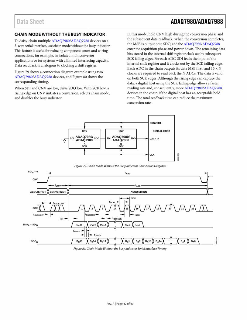
Data Sheet ADAQ7980/ADAQ7988
Rev. A | Page 42 of 49
CHAIN MODE WITHOUT THE BUSY INDICATOR To daisy-chain multiple ADAQ7980/ADAQ7988 devices on a 3-wire serial interface, use chain mode without the busy indicator. This feature is useful for reducing component count and wiring connections, for example, in isolated multiconverter applications or for systems with a limited interfacing capacity. Data readback is analogous to clocking a shift register.
Figure 79 shows a connection diagram example using two ADAQ7980/ADAQ7988 devices, and Figure 80 shows the corresponding timing.
When SDI and CNV are low, drive SDO low. With SCK low, a rising edge on CNV initiates a conversion, selects chain mode, and disables the busy indicator.
In this mode, hold CNV high during the conversion phase and the subsequent data readback. When the conversion completes, the MSB is output onto SDO, and the ADAQ7980/ADAQ7988 enter the acquisition phase and power down. The remaining data bits stored in the internal shift register clock out by subsequent SCK falling edges. For each ADC, SDI feeds the input of the internal shift register and it clocks out by the SCK falling edge. Each ADC in the chain outputs its data MSB first, and 16 × N clocks are required to read back the N ADCs. The data is valid on both SCK edges. Although the rising edge can capture the data, a digital host using the SCK falling edge allows a faster reading rate and, consequently, more ADAQ7980/ADAQ7988 devices in the chain, if the digital host has an acceptable hold time. The total readback time can reduce the maximum conversion rate.
DIGITAL HOST
CONVERT
CLK
DATA INADAQ7980/ADAQ7988 SDOSDI
CNV
ASCK
ADAQ7980/ADAQ7988 SDOSDI
CNV
BSCK
1506
0-08
4
Figure 79. Chain Mode Without the Busy Indicator Connection Diagram
tCONV
tCYC
tSSDISCK
tSCKL
tSCK
tHSDISCK
tACQ
ACQUISITION
tSSCKCNV
ACQUISITION
tSCKH
CONVERSION
SDOA = SDIB
tHSCKCNV
SCK
CNV
SDIA = 0
SDOB
tEN
DA15 DA14 DA13
DB15 DB14 DB13 DB1 DB0 DA15 DA14 DA0DA1
DA1 DA0
tHSDO
1 2 3 15 16 1714 18 30 31 32
tDSDO
1506
0-08
5
Figure 80. Chain Mode Without the Busy Indicator Serial Interface Timing
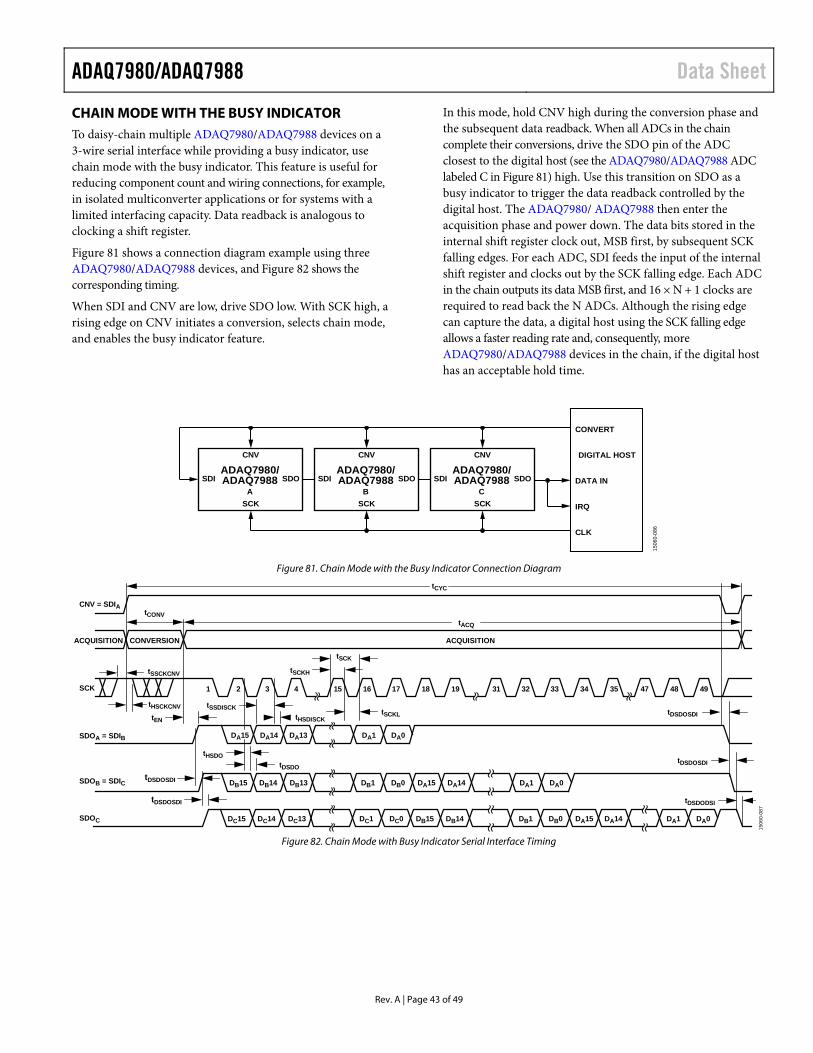
ADAQ7980/ADAQ7988 Data Sheet
Rev. A | Page 43 of 49
CHAIN MODE WITH THE BUSY INDICATOR To daisy-chain multiple ADAQ7980/ADAQ7988 devices on a 3-wire serial interface while providing a busy indicator, use chain mode with the busy indicator. This feature is useful for reducing component count and wiring connections, for example, in isolated multiconverter applications or for systems with a limited interfacing capacity. Data readback is analogous to clocking a shift register.
Figure 81 shows a connection diagram example using three ADAQ7980/ADAQ7988 devices, and Figure 82 shows the corresponding timing.
When SDI and CNV are low, drive SDO low. With SCK high, a rising edge on CNV initiates a conversion, selects chain mode, and enables the busy indicator feature.
In this mode, hold CNV high during the conversion phase and the subsequent data readback. When all ADCs in the chain complete their conversions, drive the SDO pin of the ADC closest to the digital host (see the ADAQ7980/ADAQ7988 ADC labeled C in Figure 81) high. Use this transition on SDO as a busy indicator to trigger the data readback controlled by the digital host. The ADAQ7980/ ADAQ7988 then enter the acquisition phase and power down. The data bits stored in the internal shift register clock out, MSB first, by subsequent SCK falling edges. For each ADC, SDI feeds the input of the internal shift register and clocks out by the SCK falling edge. Each ADC in the chain outputs its data MSB first, and 16 × N + 1 clocks are required to read back the N ADCs. Although the rising edge can capture the data, a digital host using the SCK falling edge allows a faster reading rate and, consequently, more ADAQ7980/ADAQ7988 devices in the chain, if the digital host has an acceptable hold time.
ADAQ7980/ADAQ7988
CSDOSDI DATA IN
IRQ
DIGITAL HOST
CONVERT
CLK
CNV
SCK
ADAQ7980/ADAQ7988
BSDOSDI
CNV
SCK
ADAQ7980/ADAQ7988
ASDOSDI
CNV
SCK
1506
0-08
6
Figure 81. Chain Mode with the Busy Indicator Connection Diagram
tCONV
tCYC
tSSDISCK
tSCKH
tSCK
tHSDISCK
tACQ
tDSDOSDI
tDSDOSDI
tDSDODSI
ACQUISITION
tSSCKCNV
ACQUISITION
tSCKL
CONVERSION
tHSCKCNV
SCK
CNV = SDIA
SDOA = SDIB
SDOB = SDIC
SDOC
tEN
DA15 DA14 DA13
DB15 DB14 DB13
DC15 DC14 DC13
DB1 DB0 DA15 DA14 DA1 DA0
DC1 DC0 DB15 DB14 DA0DA1DB0DB1 DA14DA15
DA1 DA0
tHSDO
1 2 3 15 16 174 18 19 31 32 33 34 35 47 48 49
tDSDOtDSDOSDI
tDSDOSDI
1506
0-08
7
Figure 82. Chain Mode with Busy Indicator Serial Interface Timing
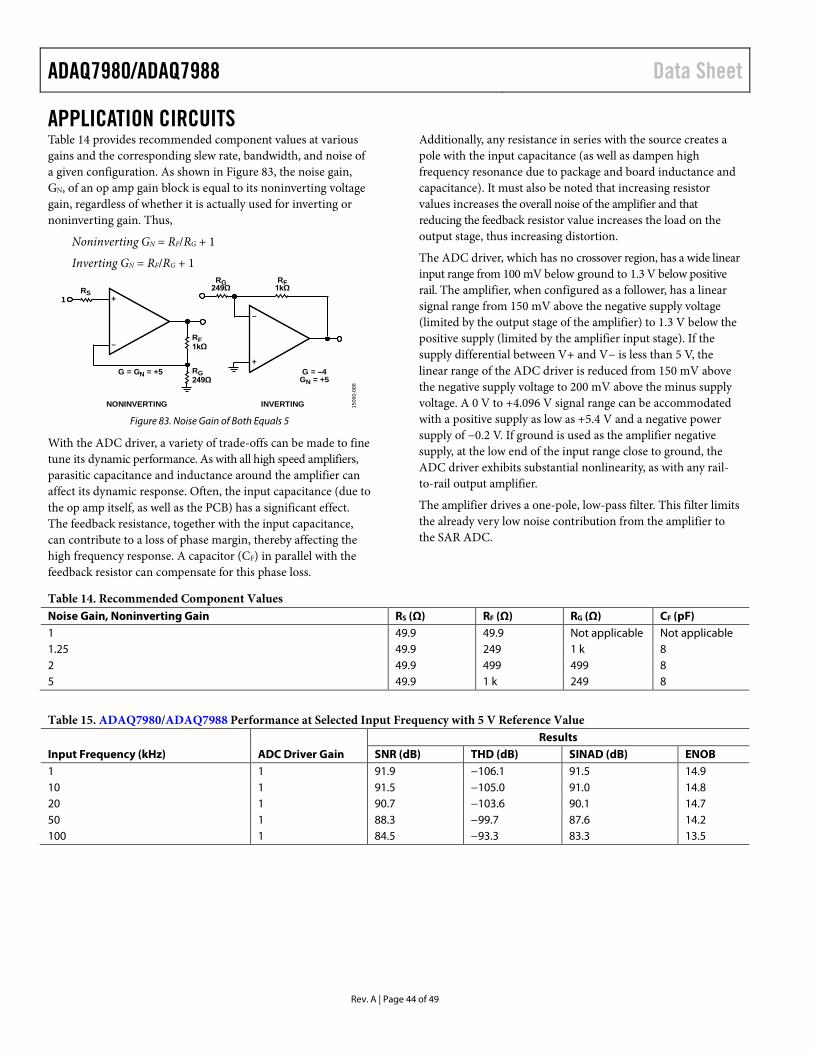
ADAQ7980/ADAQ7988 Data Sheet
Rev. A | Page 44 of 49
APPLICATION CIRCUITS Table 14 provides recommended component values at various gains and the corresponding slew rate, bandwidth, and noise of a given configuration. As shown in Figure 83, the noise gain, GN, of an op amp gain block is equal to its noninverting voltage gain, regardless of whether it is actually used for inverting or noninverting gain. Thus,
Noninverting GN = RF/RG + 1
Inverting GN = RF/RG + 1
+
–
–
+
NONINVERTING
1RS
G = GN = +5
RF1kΩ
RG249Ω
RF1kΩ
RG249Ω
G = –4GN = +5
INVERTING 1506
0-08
8
Figure 83. Noise Gain of Both Equals 5
With the ADC driver, a variety of trade-offs can be made to fine tune its dynamic performance. As with all high speed amplifiers, parasitic capacitance and inductance around the amplifier can affect its dynamic response. Often, the input capacitance (due to the op amp itself, as well as the PCB) has a significant effect. The feedback resistance, together with the input capacitance, can contribute to a loss of phase margin, thereby affecting the high frequency response. A capacitor (CF) in parallel with the feedback resistor can compensate for this phase loss.
Additionally, any resistance in series with the source creates a pole with the input capacitance (as well as dampen high frequency resonance due to package and board inductance and capacitance). It must also be noted that increasing resistor values increases the overall noise of the amplifier and that reducing the feedback resistor value increases the load on the output stage, thus increasing distortion.
The ADC driver, which has no crossover region, has a wide linear input range from 100 mV below ground to 1.3 V below positive rail. The amplifier, when configured as a follower, has a linear signal range from 150 mV above the negative supply voltage (limited by the output stage of the amplifier) to 1.3 V below the positive supply (limited by the amplifier input stage). If the supply differential between V+ and V− is less than 5 V, the linear range of the ADC driver is reduced from 150 mV above the negative supply voltage to 200 mV above the minus supply voltage. A 0 V to +4.096 V signal range can be accommodated with a positive supply as low as +5.4 V and a negative power supply of −0.2 V. If ground is used as the amplifier negative supply, at the low end of the input range close to ground, the ADC driver exhibits substantial nonlinearity, as with any rail-to-rail output amplifier.
The amplifier drives a one-pole, low-pass filter. This filter limits the already very low noise contribution from the amplifier to the SAR ADC.
Table 14. Recommended Component Values Noise Gain, Noninverting Gain RS (Ω) RF (Ω) RG (Ω) CF (pF) 1 49.9 49.9 Not applicable Not applicable 1.25 49.9 249 1 k 8 2 49.9 499 499 8 5 49.9 1 k 249 8
Table 15. ADAQ7980/ADAQ7988 Performance at Selected Input Frequency with 5 V Reference Value
Results
Input Frequency (kHz) ADC Driver Gain SNR (dB) THD (dB) SINAD (dB) ENOB 1 1 91.9 −106.1 91.5 14.9 10 1 91.5 −105.0 91.0 14.8 20 1 90.7 −103.6 90.1 14.7 50 1 88.3 −99.7 87.6 14.2 100 1 84.5 −93.3 83.3 13.5

Data Sheet ADAQ7980/ADAQ7988
Rev. A | Page 45 of 49
NONUNITY GAIN CONFIGURATIONS Figure 84 shows a typical connection diagram and the major dc error sources. The ideal transfer function (all error sources set to 0 and infinite dc gain) can be written as
ING
FIP
G
FOUT V
RRV
RRV ×
−×
+= 1 (1)
RG– VIN +
RS– VIP +
IB+
IB– + VOUT –
RF
+ VOS –
1506
0-08
9
Figure 84. Typical ADC Driver Connection Diagram and DC Error Sources
This function reduces to the following familiar forms for noninverting and inverting op amp gain expressions.
IPG
FOUT V
RRV ×
+= 1 (2)
(Noninverting gain, VIN = 0 V)
ING
FOUT V
RRV ×
−= (3)
(Inverting gain, VIP = 0 V)
The total output voltage error is the sum of errors due to the amplifier offset voltage and input currents. Estimate the output error due to the offset voltage by the following:
+×
+
−++
=
G
FOUTPNOMPOFFSET
OUT
RR
AV
PSRRVV
CMRRVCMV
V
NOM
ERROR
1 (4)
where:
NOMOFFSETV is the offset voltage at the specified supply voltage,
which is measured with the input and output at midsupply. VCM is the common-mode voltage. VP is the power supply voltage.
NOMpV is the specified power supply voltage.
CMRR is the common-mode rejection ratio. PSRR is the power supply rejection ratio. A is the dc open-loop gain.
Estimate the output error due to the input currents by the following:
+− ×
+×−
+×
=
BG
FSB
G
FGF
OUT
IRR
RIRR
RR
VERROR
11)||( (5)
Note that setting RS equal to RF||RG compensates for the voltage error due to the input bias current.
Figure 85 shows the ADC driver noninverting gain connection. The circuit was tested with multiple gain settings and an output voltage of approximately 5 V p-p for optimum resolution and noise performance.
REF
GND
VDD
VIO 1.8V TO 5V
100nFSDISCKSDOCNV
20Ω
V+
V–
1.8nF
10µFLDO
2.2µF
REF
_OU
T
LDO
_OU
T
PD_REF
AMP_OUT
PD_AMP
PD_LDO
ADC
ADCN
IN+
IN–
ADAQ7980/ADAQ7988RG
499Ω
2.2µF100nF REF1
POSITIVESUPPLY
49.9Ω
49.9Ω50Ω
RF499Ω
OPTIONAL CF
NEGATIVESUPPLY
100nF
1506
0-09
0
Figure 85. Noninverting ADC Driver, Gain = 2
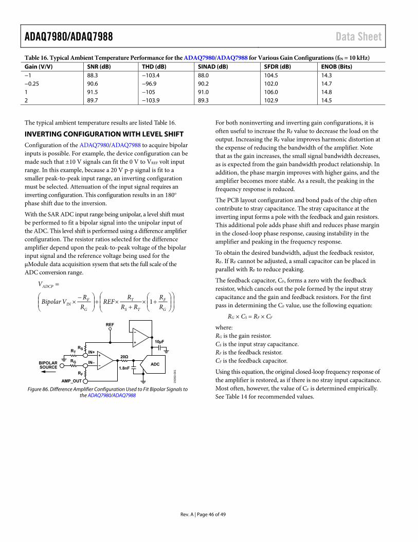
ADAQ7980/ADAQ7988 Data Sheet
Rev. A | Page 46 of 49
Table 16. Typical Ambient Temperature Performance for the ADAQ7980/ADAQ7988 for Various Gain Configurations (fIN = 10 kHz) Gain (V/V) SNR (dB) THD (dB) SINAD (dB) SFDR (dB) ENOB (Bits) −1 88.3 −103.4 88.0 104.5 14.3 −0.25 90.6 −96.9 90.2 102.0 14.7 1 91.5 −105 91.0 106.0 14.8 2 89.7 −103.9 89.3 102.9 14.5
The typical ambient temperature results are listed Table 16.
INVERTING CONFIGURATION WITH LEVEL SHIFT Configuration of the ADAQ7980/ADAQ7988 to acquire bipolar inputs is possible. For example, the device configuration can be made such that ±10 V signals can fit the 0 V to VREF volt input range. In this example, because a 20 V p-p signal is fit to a smaller peak-to-peak input range, an inverting configuration must be selected. Attenuation of the input signal requires an inverting configuration. This configuration results in an 180o phase shift due to the inversion.
With the SAR ADC input range being unipolar, a level shift must be performed to fit a bipolar signal into the unipolar input of the ADC. This level shift is performed using a difference amplifier configuration. The resistor ratios selected for the difference amplifier depend upon the peak-to-peak voltage of the bipolar input signal and the reference voltage being used for the μModule data acquisition sysem that sets the full scale of the ADC conversion range.
G
F
TS
T
G
FIN
ADCP
RR
RRR
REFRR
VBipolar
V
1
ADC
10µF
RT
RG
20Ω
RF
RS
REF
1.8nF
AMP_OUT
IN–
IN+
BIPOLARSOURCE
1506
0-09
1
Figure 86. Difference Amplifier Configuration Used to Fit Bipolar Signals to
the ADAQ7980/ADAQ7988
For both noninverting and inverting gain configurations, it is often useful to increase the RF value to decrease the load on the output. Increasing the RF value improves harmonic distortion at the expense of reducing the bandwidth of the amplifier. Note that as the gain increases, the small signal bandwidth decreases, as is expected from the gain bandwidth product relationship. In addition, the phase margin improves with higher gains, and the amplifier becomes more stable. As a result, the peaking in the frequency response is reduced.
The PCB layout configuration and bond pads of the chip often contribute to stray capacitance. The stray capacitance at the inverting input forms a pole with the feedback and gain resistors. This additional pole adds phase shift and reduces phase margin in the closed-loop phase response, causing instability in the amplifier and peaking in the frequency response.
To obtain the desired bandwidth, adjust the feedback resistor, RF. If RF cannot be adjusted, a small capacitor can be placed in parallel with RF to reduce peaking.
The feedback capacitor, CF, forms a zero with the feedback resistor, which cancels out the pole formed by the input stray capacitance and the gain and feedback resistors. For the first pass in determining the CF value, use the following equation:
RG × CS = RF × CF
where: RG is the gain resistor. CS is the input stray capacitance. RF is the feedback resistor. CF is the feedback capacitor.
Using this equation, the original closed-loop frequency response of the amplifier is restored, as if there is no stray input capacitance. Most often, however, the value of CF is determined empirically. See Table 14 for recommended values.

Data Sheet ADAQ7980/ADAQ7988
Rev. A | Page 47 of 49
USING THE ADAQ7980/ADAQ7988 WITH ACTIVE FILTERS The low noise and high gain bandwidth of the ADC driver make it an excellent choice in active filter circuits. Most active filter literature provides resistor and capacitor values for various filters but neglects the effect of the finite bandwidth of the op amp on filter performance; ideal filter response with infinite loop gain is implied. Unfortunately, real filters do not behave in this manner. Instead, they exhibit finite limits of attenuation, depending on the gain bandwidth of the active device. Optimal low-pass filter performance requires an op amp with high gain bandwidth for attenuation at high frequencies, and low noise and high dc gain for low frequency, pass-band performance.
Figure 87 shows the schematic of a second-order, low-pass active filter and lists typical component values for filters having a Bessel type response with a gain of 2 and a gain of 5.
IN+
IN–
RF
R2R1
C1
RG
C2
VIN
AMP_OUT
1506
0-09
2
Figure 87. Schematic of a Second-Order, Low-Pass Active Filter
Table 17. Typical Component Values for Second-Order, Low-Pass Active Filter of Figure 87 Gain R1 (Ω) R2 (Ω) RF (Ω) RG (Ω) C1 (nF) C2 (nF) 2 71.5 215 499 499 10 10 5 44.2 365 365 90.9 10 10
Figure 88 is a network analyzer plot of the performance of this filter.
1k 10k 100k 1M 10M
FREQUENCY (Hz)
50
40
30
20
10
0
–10
–20
–30
–40
–50
GA
IN (
dB
)
G = 2
G = 5
1506
0-09
3
Figure 88. Frequency Response of the Filter Circuit of Figure 87 for Two
Different Gains

ADAQ7980/ADAQ7988 Data Sheet
Rev. A | Page 48 of 49
APPLICATIONS INFORMATION LAYOUT Heat dissipation from the package can be improved by increasing the amount of copper attached to the pins of the ADAQ7980/ADAQ7988. However, a point of diminishing returns is eventually reached, beyond which an increase in the copper size does not yield significant heat dissipation benefits.
When designing the PCB, separate and confine the analog and digital sections to certain areas of the PCB that houses the ADAQ7980/ADAQ7988. The ADAQ7980/ADAQ7988 pinouts with all their analog signals on the left side and all their digital signals on the right side eases this task.
Avoid running digital lines under the devices because these couple noise onto the die, unless using a ground plane under the ADAQ7980/ADAQ7988 as a shield. Never run fast switching signals, such as CNV or clocks, near the analog signal paths. Avoid crossover of digital and analog signals.
Use at least one ground plane, and it can be common or split between the digital and analog section. In the latter case, join the planes underneath the ADAQ7980/ADAQ7988 devices.
Finally, decouple the power supplies (V+, V−, VDD, and VIO) of the ADAQ7980/ADAQ7988 with low ESR ceramic capacitors that are placed close to the ADAQ7980/ADAQ7988 and that are connected using short and wide traces to provide low impedance paths and reduce the effect of glitches on the power supply lines.
Place the smallest value capacitor on the same side of the board as the ADAQ7980/ADAQ7988 and as close as possible to the amplifier power supply pins. Connect the ground end of the capacitor directly to the ground plane.
See Figure 89 for an example layout of the ADAQ7980/ ADAQ7988 that can save 50% PCB area compared to similar designs using individual components for each section of the μModule data acquisition system.
EVALUATING THE PERFORMANCE OF THE ADAQ7980/ADAQ7988 The evaluation board (EVAL-ADAQ7980SDZ) user guide for the ADAQ7980/ADAQ7988 outlines the other recommended layouts for the ADAQ7980/ADAQ7988.
The evaluation board package includes a fully assembled and tested evaluation board, documentation, and software for controlling the board from a PC via the separately purchased EVAL-SDP-CB1Z.
1506
0-29
0
ADAQ7980/ADAQ7988
PIN 1
Figure 89. Example Layout for the ADAQ7980/ADAQ7988

Data Sheet ADAQ7980/ADAQ7988
Rev. A | Page 49 of 49
OUTLINE DIMENSIONS
09-1
1-20
15-A
PKG
-004
990
BOTTOM VIEWTOP VIEW
SIDE VIEW
2.081.981.88
1.65 REF
0.3620.3320.302
0.450.400.35
0.300.250.20
5.105.004.90
4.104.003.90
PIN 1CORNER AREA
1
5
612
13
17
18 24
0.50BSC
0.10REF
2.00 REF
3.00 REFPIN 1INDICATOR
Figure 90. 24-Lead Land Grid Array [LGA]
5 mm × 4 mm Body and 1.98 mm Package Height (CC-24-2)
Dimensions shown in millimeters
ORDERING GUIDE Model1 Temperature Range Package Description Package Option ADAQ7980BCCZ −55°C to +125°C 24-Lead Land Grid Array [LGA] CC-24-2 ADAQ7980BCCZ-RL7 −55°C to +125°C 24-Lead Land Grid Array [LGA] CC-24-2 ADAQ7988BCCZ −55°C to +125°C 24-Lead Land Grid Array [LGA] CC-24-2 ADAQ7988BCCZ-RL7 −55°C to +125°C 24-Lead Land Grid Array [LGA] CC-24-2 EVAL-ADAQ7980SDZ Evaluation Board EVAL-SDP-CB1Z Evaluation Controller Board 1 Z = RoHS Compliant Part.
©2017 Analog Devices, Inc. All rights reserved. Trademarks and registered trademarks are the property of their respective owners. D15060-0-8/17(A)