11 3891 texas 77710, u.s.a. 11 3891 abstract new technologies are being developed to provide lower...
TRANSCRIPT
ECONOMICS OF POLYSILICON PROCESSES
Carl L. Yaws, K. Y. L i and S. M. Chou Lamar University
Beaumont, Texas 77710, U.S.A. 11 3891
ABSTRACT
New technologies are being developed to provide lower cost polysilicon material for solar cells. Existing technology which normally provides semiconductor industry polysilicon material is undergoing changes and also being used to provide polysilicon material for solar cells.
Economics of new and existing technologies are presented for producing polysilicon. The economics are primarily based on the preliminary process design of a plant to produce 1,000 metric tons/year of silicon. The polysilicon processes include: Siemen s process (hydrogen reduction of trichlorosilane); Union Carbide process (silane decomposition) and Hemlock Semiconductor process (hydrogen reduction of dichlorosilane). The economics include cost estimates of capital investment and product cost to produce the polysilicon via the technology. Sensitivity analysis results are also presented to disclose the effect of major parameters such as utilities, labor, raw materials and capital investment.
https://ntrs.nasa.gov/search.jsp?R=19860017211 2018-07-08T15:24:22+00:00Z
1. INTRODUCTION
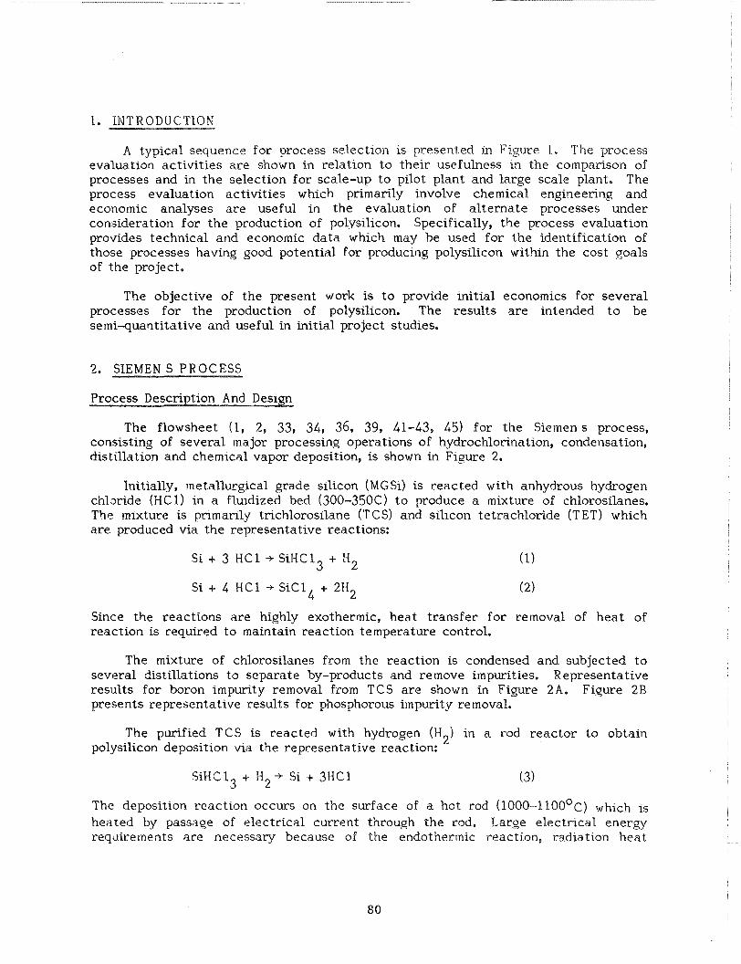
A typical sequence for process selection is presented in Figure 1, The process evaluation activities are shown in relation t o their usefulness in the comparison of processes and in the selection for scale-up to pilot plant and large scale plant. The process evaluation activities which primarily involve chemical engineering and economic analyses are useful in the evaluation of alternate processes under consideration for the production of polysilicon. Specifically, the process evaluation provides technical and economic data which may he used for the identification of those processes having good potential for producing polysilicon within the cost goals of the project,
The objective of the present work is t o provide initial economics for several processes for the production of polysilicon. The results are intended t o be semi-quantitative and useful in initial project studies.
3,. SIEMEN S PROCESS
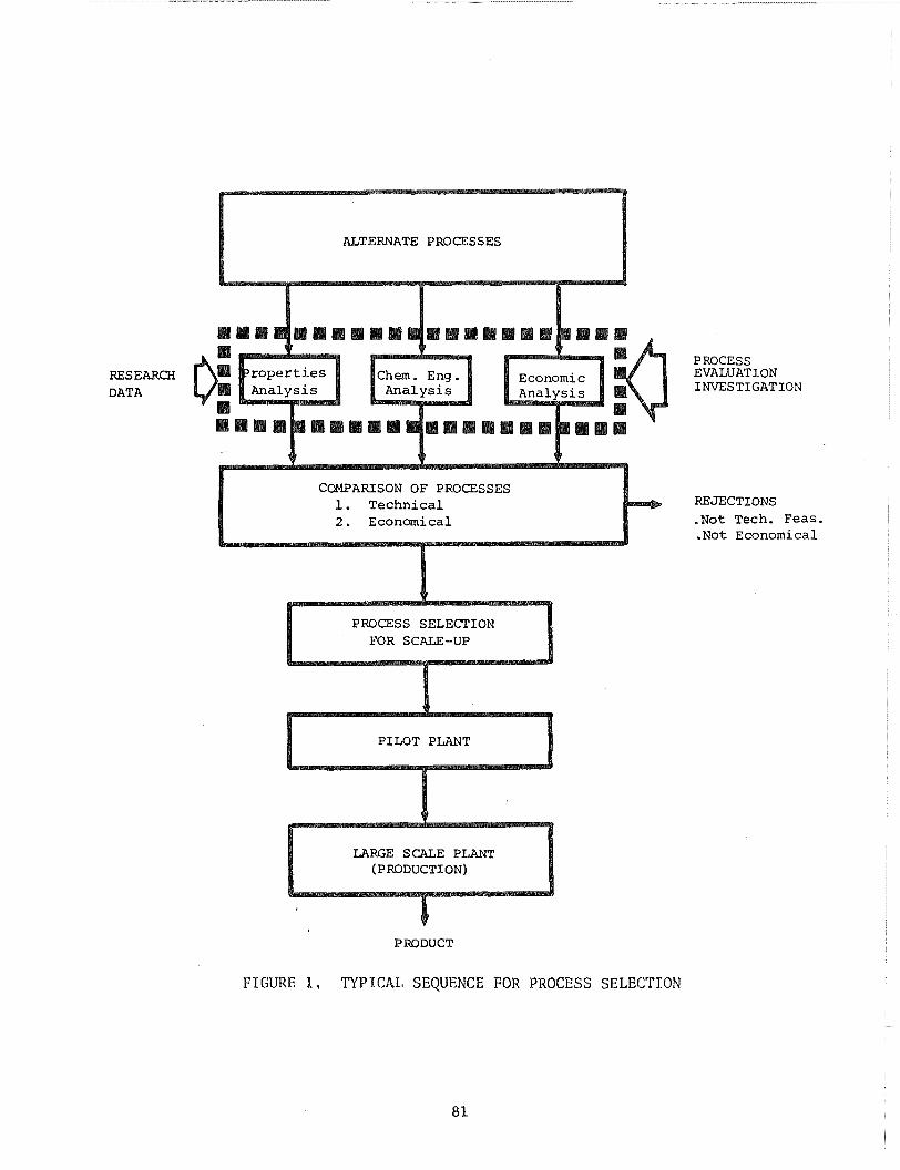
The flowsheet (1, 2, 33, 34, 36, 39, 41-43, 45) for the Siemens process, consisting of several rnajor processing operations of hydrochlorination, condensation, distillation and chemical vapor deposition, is shown in Figure 2.
Initially, metallilrgical grade silicon (MGSi) is reacted with anhydrous hydrogen chloride (HC1) in a fluidized bed (300-350C) t o produce a mixture of chlorosilanes. The mixture is primarily trichlorosilane (T C S) and silicon tetrachloride (T ET) which are produced via the representative reactions:
Since the reactions are highly exothermic, heat transfer for removal of heat of reaction is required to maintain reaction temperature control.
The mixture of chlorosilanes from the reaction is condensed and subjected to several distillations to separate by-products and remove impurities. Representative results for boron impurity removal from TCS are shown in Figure 2 A . Figure 2R presents representative results for phosphorous impurity removal.
The purified TCS is reacted with hydrogen ( H Z ) in a rod reactor to obtain polysilicon deposition via the representative reaction:
The deposition reaction occurs on the surface of a hot rod ( 1 0 0 0 - 1 1 0 0 ~ ~ ) which is heated by passage of electrical current through the rod. Large electrical energy reqllirements are necessary because of the endothermic reaction, radiation heat
ALTERNATE PROCESSES
PROCESS RESEARCH EVALUATION DATA INVESTIGATION
1. T e c h n i c a l REJECTIONS 2 . E c o n o m i c a l . N o t T e c h . F e a s . . N o t E c o n o m i c a l
LARGE SCALE PLANT (PRODUCTION)
PRODUCT
FIGURE 1, TYPICAL SEQUENCE FOR PROCESS SELECTION

R e f l u x R a t i o , R
FIGUaE 2A. REPRESENTATIVE RESULTS FOR BORON IMPURITY REMOVAL

Reflux R a t i o , R
FIGURE 2B. REPRESENTATIVE: RESULTS FOR PHOSPHORUS IMPURITY REMOVAL

losses and incomplete conversion of the TCS, Unreacted chlorosilanes, hydrogen chloride and hydrogen are separated and recycled.
A representative polysilicon deposition reactor using trichlorosilane as the silicon source material is shown in Figure 3.
In the chemical engineerinp analysis of the process, a process design was performed to obtain data for the cost analysis. The design was based on a plant for the production of 1,900 metric tons/yr of polysilicon via the Siemens process. The detailed design included TCS production in a fluidized bed; TCS purification by distillation; silicon production by chemical vapor deposition in a Siemen s type rod reactor; recycle of chlorosilanes, hydrogen chloride, and hydrogen; waste treatment provisions to meet environmental quality; and storape considerations for feed, in-process and product materials.
The process design provided detailed data for raw materials, utilities, major process equipment and production labor requirements which are necessary for polysilicon production. .
The cost analysis results for producing silicon by this technology are presented in Table 1 including costs for raw materials, labor, utilities and other items composing the product cost (total cost of producing silicon). The tabulation summarizes all of these items to give a total product cost without profit of 29.49 $ k g Si (1985 dollars). This product cost without profit includes direct manufacturing cost, indirect manufacturing cost, plant overhead and general expenses.
The economic summary for the process is given in Table 2. Results for process, plant size, plant product, plant investment, profitability analysis and sensitivity analysis are displayed in the tabulation.
A sensitivity analysis was peformed t o determine the influence of cost parameters on the economics of producing silicon by this technology. The cost sensitivity results are given in Figure 4 in which product cost ($/kg Si) is plotted vs variation (-100 t o 0 t o +I00 percent) of the primary cost parameters (raw materials, labor and utilities). The O per cent variation represents the base case. The -100 per cent variation corresponds to the case of no costs for the parameter; and the +I00 per cent represents the case for a doubling of cost for each parameter. The plot illustrates that product cost is greatly influenced by utilities (electrical energy).
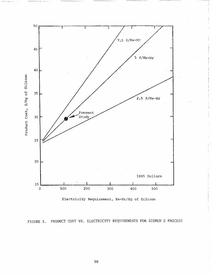
The variation of product cost ( $ / k g Si) with electrical energy requirements (kw-hr/k.g Si) is shown in Figure 5. The present study which is based on electrical energy requirements of 120 kw-hr/kg of Si and 5 Q/kw-hr is shown as the darkened circle in the figure. If electrical energy requirements are increased from 120 t o 220 kw-hr, the product cost increases from $29.5 to $34.5 per kg of Si. The increase is even more pronounced a t 7.5 Qkw-hr electricity.

uaste gases ,- electric energy
FIGURE 3. REPRESENTATIVE POLYCILICON DEPOSITION REACTION FOR TRICHLOROSILANE ( GOVERNMENT REPORT: CISZEK (2) )
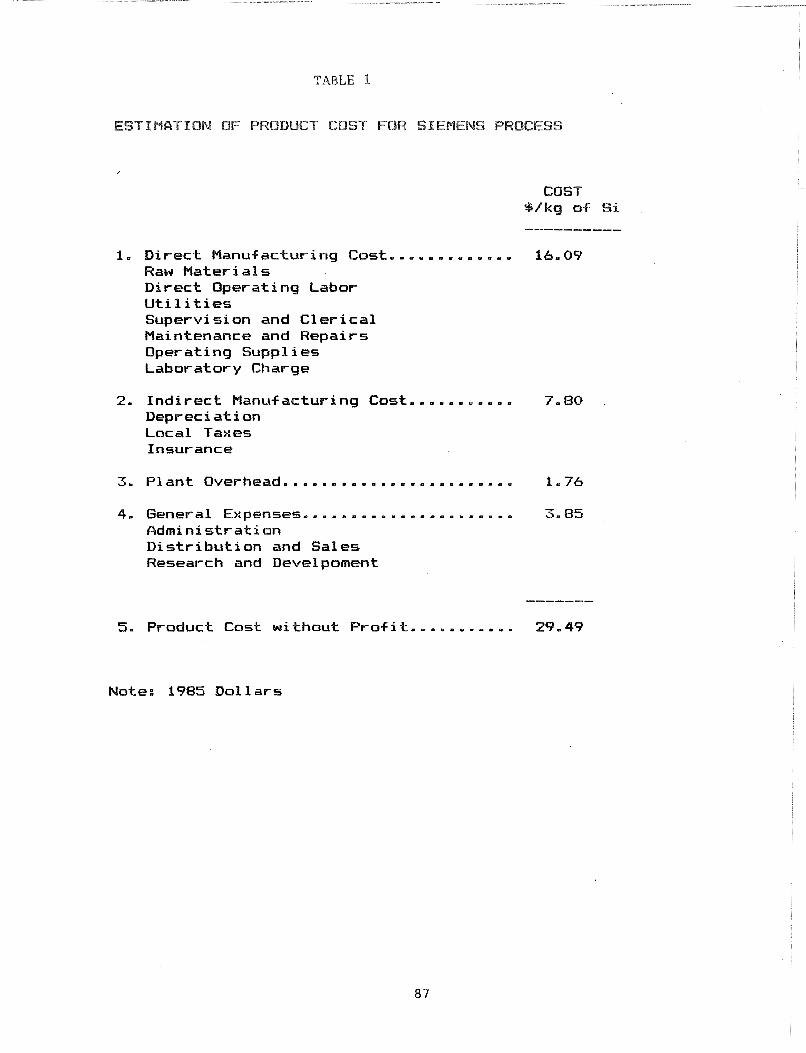
TABLE 1.
ESIXMATPBN 8F PRBBUCI COST FOR SIEMENS PROCESS
............ 1. Direct Manufacturing Cost. 16- 09 Raw Materials Direct Operating Labor Utilities Supervision and Clerical Maintenance and Repairs Operating Suppl i es Laboratory Charge
.......... 2. Indirect Manufacturing Cost. 7.80 Bepreci ati on Local Taxes Insurance
3. Plant Overhead.............-..-....... 1.76
.................... 4. General Expenses.. 3.85 Administration Distribution and Sales Research and Devel poment
-------
5. Product Cost without Profit..- ........ 29.49
Note: 1985 Dollars

TABLE 2
ECBNOMlC SUMMARY: COST ANALYSIS FOR SIEMENS PRBCESS
1- process ......................... SIEMENS PRBCESS 2. Plant Size ...................... 1000 MT/yr 3 m Plant Product ----A,.----.----------- POLYS~LICON . .
4. Pl ant Investment ---------------- B 69.00 Million
Fixed Capital ---- B 60.00 Million Working Capital -- $ 9.00 Million Total Capital ---- B 69.00 Million
5. Profitability Analysis
Return on Original Investment after Taxes ( % ROI) Discounted Cash Flow Rate of Return after Taxes 4 % DCF)
Return
0 % ROI 10 % ROI 20 % ROI SO % ROI 40 % ROI 50 % ROI 60 % ROI 70 % ROI 80 % ROI 90 % ROI
100 % ROI
Sales Price %/kg of Si Return
Sales Price $/kg of Si
0 % DCF 10 % DCF 20 % DCF SO % DCF 40 % DCF 50 % DCF 60 % DCF 70 % DCF 80 % DCF 90 % DCF
100 % DCF
Based on 10 year project life and 10 year straight line depreciation. Tax rate (federal) of 46 %,
6. Sensitivity Analysis Product Cost, $/kg of Si
-100% -50% BASE 950% +10OX DELTA ----- ----- ----- ----- ----- -----
Raw Materi a1 s 25.40 27.45 29.49 31.54 33.58 4.09 Labor 27-60 28.54 29.49 50.44 31.39 1-90 Utilities 21-76 25-63 29.49 33.36 37.22 7-73 Plant Investment 17.93 23.71 29.49 35.27 41.05 11.56 (Fixed Capital
Note: 1985 Dollars

Var ia t ion , %
FIGURE 4 , SENSITIVIIFY PLOT FOR SIEMEN S PROCESS
0 100 200 300 400 500
E l e c t r i c i t y Requirement, KW-~r/Kg of S i l i c o n
FIGURE 5. PRODUCT COST VS. ELECTRICITY REQUIREMENTS FOR SIEMEN S PROCESS

2. UNION CARBIDE PROCESS
The Union Carbide process (7-9, 27, 36, 39) for silicon involves several processing operations of hydrogenation-hydrochlorination reaction, stripping, distillation, redistribution reaction, silane purification, and silicon deposition. The process flowsheet is shown in Figure 6.
Hydrogen, silicon tetrachloride, and metallurigical grade silicon are fed to the hydrogenation reactor (fluidized bed, SOOC, 515 psia, copper catalyst) t o produce a mixture of chlorosilanes. The mixture of chlorosilsnes from the hydrogenation reaction is condensed and subjected t o several distillations to separate components and remove impurities.
Initially, the condensed liquid mixture is sent to D-01 stripper (90 psia) to remove inert gases and volatile impurities. The stripper bottoms go t o D-02 distillation (55 psia) which separates T C S (trichlorosilane) and T$ T (silicon tetrachloride). The TCS redistribution reactor (liquid phase, 85 psia, 140 F catalyst) is used to produce DCS (dichlorosilane). The separation of DCS and TCS is achieved in D-03 distillation (320 psia). The overhead goes to DCS redistribution reactor (liquid phase, 510 psia, 140 F, catalyst) t o produce silane (SiH 1. The silane is purified by separation from trace impurities (such a s R2H6) by 6-04 distillation (355 psia). Representative results for diborane impurity removal are shown in Figure 6 A .
The purified silane is mixed with hydrogen and then introduced into the deposition reactor (Komatsu license, 7 ) t o produce silicon via the representative reaction:
The reaction occurs in a deposition reactor which is heated by passage of electrical current through the silicon rods to attain a temperature in the 800-900C range (21, 22). Deposition rates of 4-8 micrometers/rnin of silicon on the rod surface are reported in the Komatscl patents.
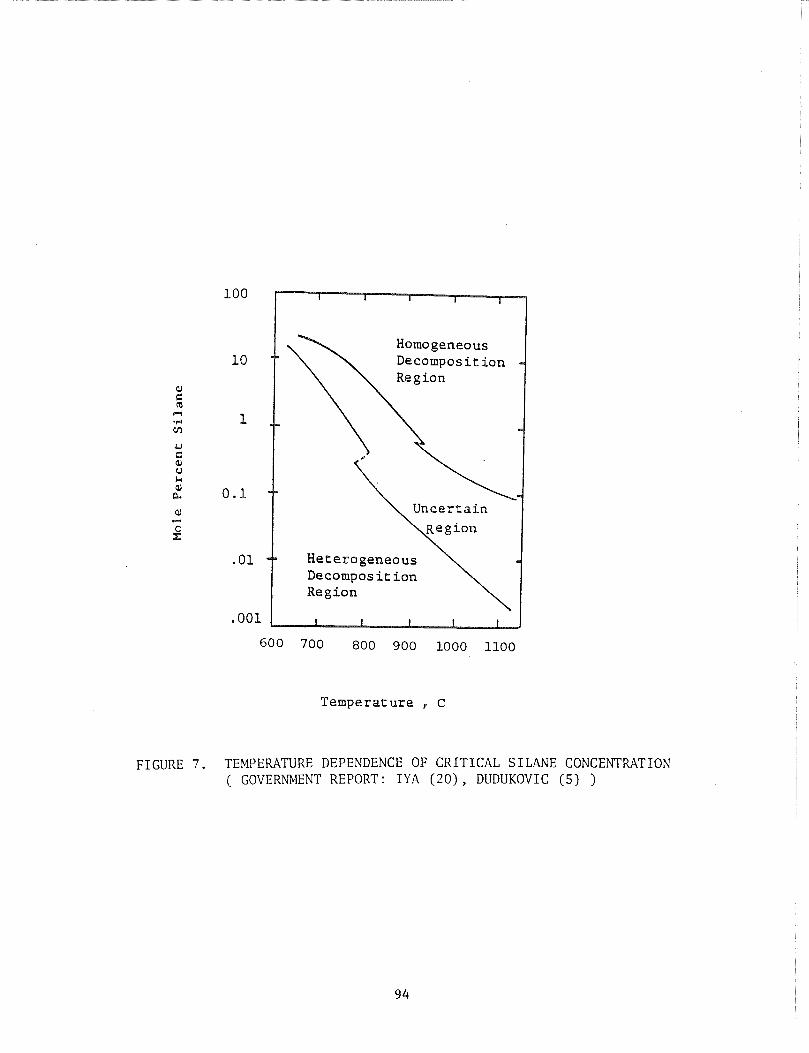
For the deposition reactor, the homogeneous decomposition reaction resulting in silicon dust for mation is not desireable. The heterogeneous decomposition reaction resulting in silicon deposition on the rod surface is desirable. The temperature dependence of critical silane concentration for homogeneous and heterogeneous decomposition regions has been studied by Iya (20) and others (28). Results from the recent report of Dudukovic (5) are shown in Figure 7. At 800C, the heterogeneous decomposition region appears to be in the 1-2% concentration range for silane in hydrogen.
A representative polysilicon deposition reactor for silane is shown in Figure 8 (Kornatsu patent: 21, 22). The thermal insulator in the reaction chamber is obvious in both the side and top views. The thermal insulators provide for radiation benefits (individual silicon rods from radiation from the other red-heated. silicon rods) and for temperature control benefits for reduction of homogeneous reaction in the gas phase.


3
D i s t i l l a t i o n C o l u m n DC-4
2.5
2
1.5
1
.5
0 0 5 10 1 5 2 0 2 5
R e f l u x R a t i o , R
FIGURE 6A REPWSENTATIVE: RESULTS FOR DIBORANE IMPURITY REMOVAL
U c a.' U
Decomposition
Heterogeneous Decomposition
Temperature , c
FIGURE 7. TEMPERATURE DEPENDENCE OF C R I T I C A L S I L A N E CONCENTRATION ( GOVERNMENT REPORT: IYA (20) , DUDUKOVIC (5) )

En the chemical engineering analysis of the Union Carbide process, a process design was performed for a plant to produce 1,000 metric tons/y-r of polysilicon,
Cost analysis results for producing polysilicon via the Union Carbide process with chemical vapor deposition reactors are given in Table 3. The results indicate a product cost without profit of 24.55 $/kg Si (1985 dollars).
Table 4 presents the economic summary of results for process, plant size, plant product, plant investment, profitability analysis and sensitivity analysis. The capital investment of $74.75 million of the present study for 1,900 metric ton plant is in the range of the $85 million for a 1,500 metric ton plant reported by Union Carbide in a news release (9) and $90 million reported for a doubling of capacity to 2,400 metric tons (8).
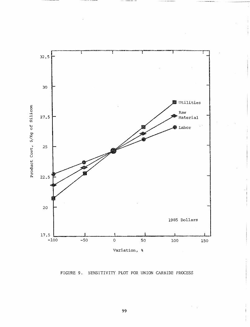
The sensitivity analysis plot is shown in Figure 9. The product cost is influenced most by utilities (electrical energy).
4. HEMLOCK SEMICONDUCTOR PROCESS
Process Descri~tion and Desien
The process flowsheet for Hemlock Semiconductor process for polysilicon is shown in Figure 10. The process involves major processing operations of hydrochlorination, separation, several distillation units, redistribution, boron removal, silicon deposition, recovery unit and waste treatment.
Metallurgical grade silicon is hydrochlorinated in the presence of hydroqen and silicon tetrachloride in a fluidized bed reactor (5OOC, 515 psia). In the process, the r e a c t i o n p r o d u c t i s s u i n g f r o m t h e h y d r o c h l o r i n a t i o n r e a c t o r (hydrochlorination-hydrogenation reaction) is cooled and undergoes a vapor-liquid flash separation. The vapor fraction containing the hydrogen from the flash is recycled back to the hydrochlorination reactor. The liquid fraction containing the chlorosilanes and dissolved gases is fed to the initial distillation column.
The function of the initial distillation column (D-01, stripper column, 90 psia) in the process is to remove volatile gases (such as hydrogen and nitrogen) which are dissolved m liquid chlorosilanes. For the engineering design, TCS (trichlorosilane) was selected as the heavy key component for the separation.
The second distillation column (D-02, TCS column, 90 psia) in the process separates TCS (trichlorosilane) and TET (silicon tetrachloride). The distillation column has three feeds (bottons fro% the third distillation, chlorosilanes from t l ~ e recovery unit and bottoms from the initial distillation). The T E T from the distillation is recycled to the hydrochlorination reactor for additional conversion.
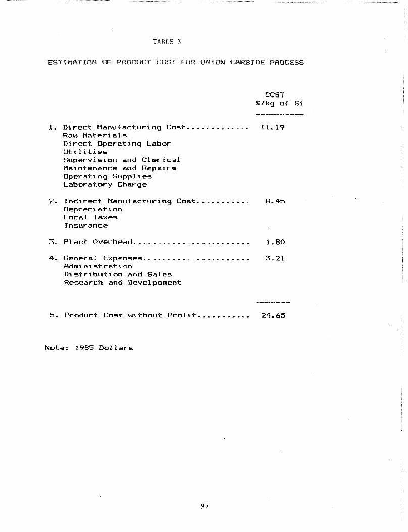
TABLE 3
ESTIM&TION OF PRODUCT COST FOR UNIBN CARBIDE PROCESS
............ 1. Direct Manufacturing Cost. 11.19 Raw Materi a1 s Direct Operating Labor Utilities Supervision and Clerical Maintenance and Repairs Operating Suppl i es Laboratory Charge
2. Indirect Manufacturing Cost........... 8-45 Depreci ati on Local Taxes Insurance
T a. Plant O v e r h e a d . . . . . . . . . . . . - . . . . . - . . . - . 1.80
..................... 4. General Expenses. 3- 21 Qdministration Distribution and Sales Research and Develpoment
5. Product Cost without Profit.. ......... 24.65
Note: 1985 Dollars
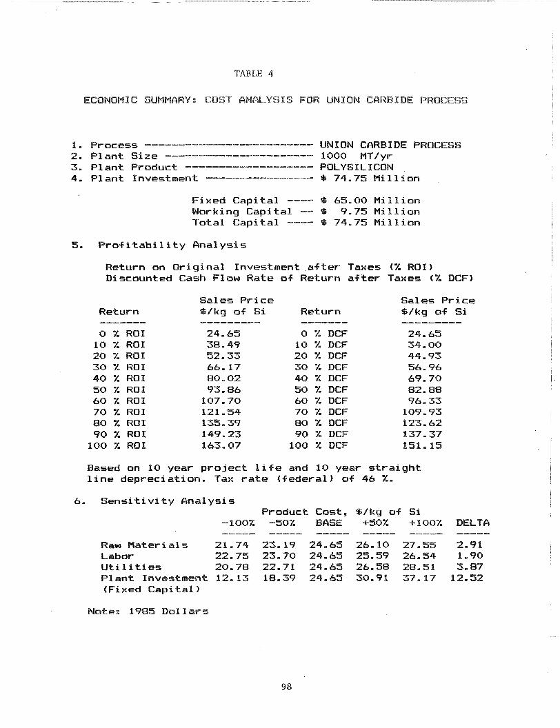
TABLE 4
ECBNBMTC SUMMARY: COST ANALYSIS FOR UNION CARBIDE PROCESS
1. process ......................... UNION CfiRBIDE PROCESS 2. Plant Size ...................... 1000 MT/yr 3, Plant Product --------.----------- POLYSILICON 4. Plant Investment ---------------- Q 74.75 Million
Fixed Capital ---- $ 65.00 Million Working Capital -- $ 9.75 Million Total Capital ---- $ 74.75 Million
5. Prof i tabi l i ty Analysis
Return on Original Investment after Taxes ( % ROI) Discounted Cash Flow Rate of Return after Taxes (% DCF)
Return Sales Price $/kg of Si Return
Sales Price $/kg of Si
0 % ROI 18 % ROI 20 % ROI 30 % ROI 40 % ROI 50 % ROI 60 % ROI 70 % ROI 80 % ROI 90 % ROI 100 % ROI
0 % DCF 10 % DCF 20 % DCF 30 % DCF 40 % DCF 50 % DCF 60 % DCF 70 % DCF 80 X DCF 90 % DCF 100 % DCF
Based on 10 year project life and 1 0 year straight line depreciation. Tax rate <federal) of 46 %.
6. Sensitivity Analysis Product Cost, $/kg af Si
-100% -50% BASE +50% +100% DELTA ----- ----- ----- ----- ----- -----
Raw Mater i a1 s 21.74 23.19 24.65 26.10 27-55 2.91 Labor 22.75 23.70 24.65 25-57 26.54 1.90 Utilities 20.78 22.71 24.65 26.58 28.51 3.87 Plant Investment 12-13 18.39 24.&5 30.91 37.17 12.52 (Fixed Capital 1
-50 0 5 0 100 L50
Var ia t ion , %
FIGURE 9. SENSITIVITY PLOT FOR UNION CARBIDE PROCESS

The TCS from the second distillation is sent to the redistribution reactor (liquid phase, 80 psia, 80C) where TCS is redistributed t o DCS and T E T accordin9 to the representative chemical reaction equation:
The conversion from pure TCS is about 10.5% to DCS.
After redistribution the stream is sent to the boron removal unit and the third distillation. The third distillation column (D-03, DCS column, 90 psia) in the process separates DCS (dichlorosilane) and T C S (trichlorosilane). D CS from the distillation is sent t o the silicon deposition reactors.
The purified DCS is reacted with hydrogen (HZ) in a rod reactor to obtain polysilicon deposition via the following representative chemical reaction equation:
The above reaction equation may include several reaction steps. Chemical equilibrium is involved and in reality, several chlorosilanes (such as SiH C1 SiHC13 and Sic1 ) are also present in the gas phase by-products.
2 2, 4
The chemical vapor deposition reaction with DCS is very fast and occurs on the surface of a hot rod (1000-1200C) which is heated by passage of electrical current through the rod. Deposition rates and conversions for dichlorosilane are approximately twice (2x1 those for the usual trichlorosilane process. Other benefits include higher molar silicon conversion and lower power consumption (25, 26).
In this process using dichlorosilane as the silicon source material, wall deposits resulting from the dichlorosilane deposition reaction are not desirable. Representative bell jar silicon deposition is shown in Figure 11. The homogeneous gas phase reaction resulting in the formation of solid silicon particles (not on the rod surface) is 31~0 not desirable. The reduction of wall deposits has been investigated by Hemlock Semiconductor (26). One approach involved an advanced decomposition reactor with a cool bell jar temperature (300C) as compared with hot bell jar reactor (750C). The study also encompassed screening of lower cost materials of construction such as stainless steels and other metallic alloys.
A process design was performed to obtain data for a cost analysis of a process plant t o produce 1,900 metric tons/yr of polysilicon via the Hemlock Semiconductor process.
Cost analysis results for producing polysilicon by the Hemlock Semiconductor process are displayed in Table 5 including raw materials, labor, utilities and other items. A total product cost without profit of 19.45 $/kg Si (1985 dollars) is indicated.
The economic summary for the process is provided in Table 6 including plant investment, profitability analysis and sensitivity analysis.
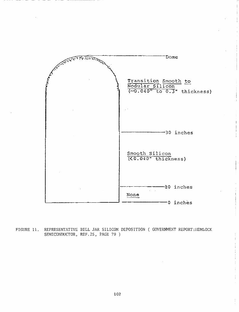
T r a n s i t i o n Smooth t o - N o d u l a r S i l i c o n ( - Q . 0 4 0 " t o 0 . 3 " t h i c k n e s s )
Smooth S i l i c o n (< 0 . 0 4 0 " t h i c k n e s s )
FIGURE 11. REPRESENTATIVE BELL JAR SILICON DEPOSITION ( GOVERNMENT REP0RT:HEMLOCK SEMICONDUCTOR, REF.25, PAGE 79 )
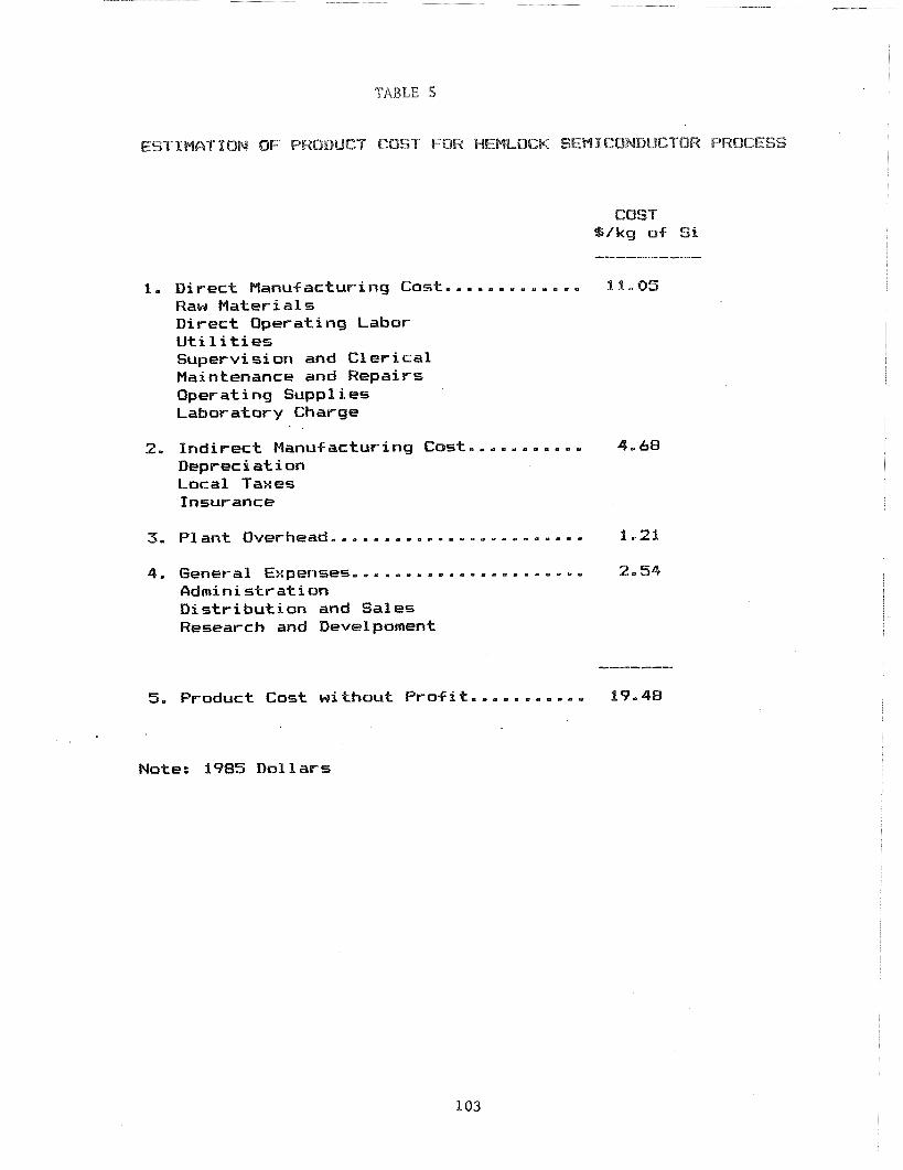
TABLE 5
ESTLMGTIBN OF PRODUCT CQST FOR HEMLOCK SEMICONDUCTOR PWBCESS
1. Direct Manufacturing Cost.. ........... I d , OS Raw Materials Direct Operating Labor Utilities Supervision and Clerical Maintenance and Repairs Oper at i ng Supp 1 i es Laboratory Charge
2. Indirect Manufacturing Co~t.......~... 4.68 Depreciation Local Taxes Insurance
3. Plant O~erhead,...............-..~..~. 1.21
...................... 4. General Expenses 2.54 Administration Distribution and Sales Research and Develpoment
......... 5. Product Cost without Prof it.. 17-48
Note: 1985 Dollars
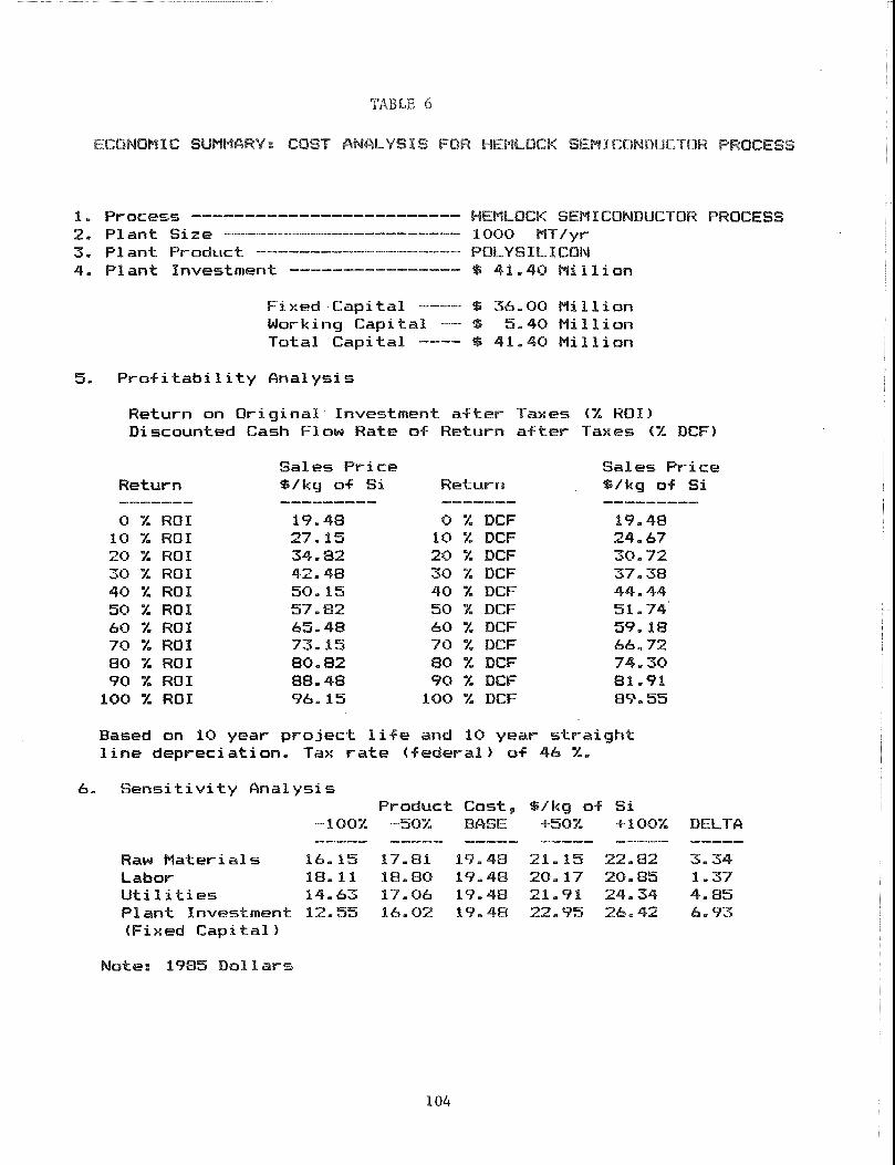

The sensitivity analysis results for primary cost parameters is displayed in Figure 12. The product cost is influenced much by utilities (electrical ener<y),
5. COST COMPARISON
A cursory cost comparison for capital investment is aade in Figure 13 for the Siemen s process. In 1980, Wacker (12) announced a $13 million capital investment for a 500 MT/yr polysilicon plant expansion (1,200-1,300 to 1,800 MT/yr). The first block in the figure shows this data. The second block with a capital investment of $31.2 million represents this data adjusted to 1,000 MT/yr expansion and 1985 dollars. The third block presents the present study. The capital investment of $69 million (complete plant) of the present study is higher than the $31.2 million (plant expansion).
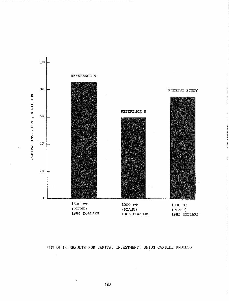
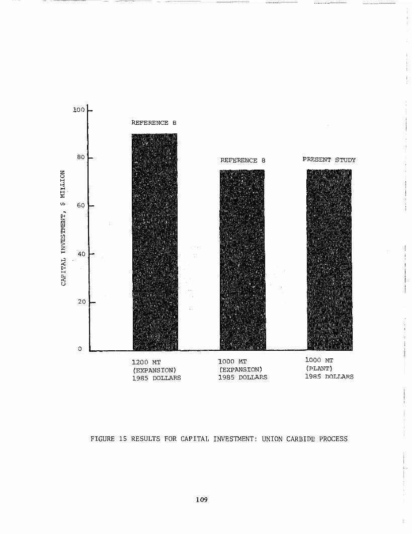
Results for capital investment for the Union Carbide process are displayed in Figures 14 and 15. In 1984, Union Carbide (9) announced its plans to start silane production in its $85 million polysilicon facility (Moses Lake, Washington) capable of producing 1,500 MT/yr. The first block in Figure 14 presents this data. The second block shows the adjusted data of $56.7 million (1,000 MT/yr, 1985 dollars). The result of $74.8 million (1,000 MT/yr, 1985 dollars) for the present study is higher. In 1985, capital investment of $90 million was reported (8) to double the capacity of the polysilicon facility to 2,400 MT annually. The adjusted value for a 1,000 M T h r is about $75 million (plant expansion). The adjusted value is about the sane as the result of $74.75 (complete plant) of the present study.
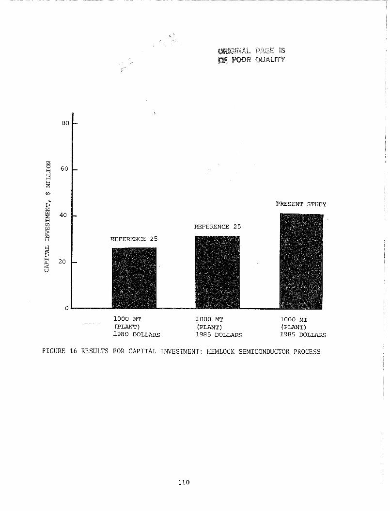
Capital investment results for the Hemlock Semiconductor process are presented in Figure 16. A capital investment of $25.21 million (1980 dollars) for 1,000 MT/yr polysilicon plant using dichlorosilane as t'le silicon source material is given in the Hemlock Semiconductor report (25). The adjusted value is $30.25 million (1985 dollars). The results of $41.40 million (1985 dollars) of the present study are higher.
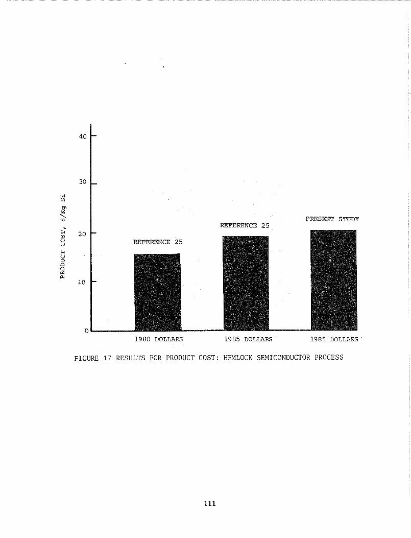
The results for product cost are shown in Figure 17 for the Hemlock Serniconductor process. A product cost for polysilicon of 15.60 $/kg (1980 dollars) is presented in the Hemlock semiconductor report (25). The adjusted value is about 18.72 $/kg (1985 dollars). The product cost of 19.48 $/kg (1985 dollars) of the present study is slightly higher. Both results suggest product cost without profit is in the 20 $/kg range.
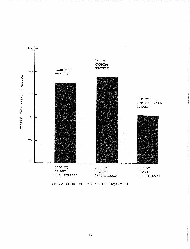
Results for capital investment are shown in Figure 18 for Siemen s, Union Carbide and Hemlock Semiconductor processes. The cursory comparison suggests that capital investment of $41.4 million for the Hemlock Semiconductor process is lower than the $69 million and $74.75 million for Siemens and Union Carbide processes,
The results for product cost are given in Figure 19. The product cost per kg of polysilicon of $29.49 for Siemen s process appears to be the highest. The $24.65 for Union Carbide process appears to be intermediate. The $19.49 for Hemlock Serniconductor process appears to be lowest.

-100 -50 0 50 10 0 150
Var ia t ion , %
FIGURE 12. SENSITIVITY PLOT FOR HEMLOCK SEMICONDUCTOR PROCESS

REFERENCE 12
P R E S E N T STUDY
REFERENCE 1 2
500 MT 1000 MT 1000 MT (EXPANSION) (EXPANS ION ) (PLANT 1980 DOLLARS 1985 DOLLARS 1985 DOLLARS
F I G U R E 13 R E S U L T S FOR CAPITAL INVESTMENT: SIEMEN S PROCESS
PRESENT STUDY
REFERENCE 9
1500 MT 1 0 0 0 MT 1 0 0 0 MT (PLANT) (PLANT) (PLANT) 1 9 8 4 DOLLARS 1 9 8 5 DOLLARS 1 9 8 5 DOLLARS
FIGURE 14 R E S U L T S FOR C A P I T A L INVESTMENT: UNION CARBIDE PROCESS
REFERENCE 8
REFERFNCE 8 PRESENT STUDY
1 2 0 0 MT 1000 MT 1000 MT
(EXPANS ION) (EXPANSION) (PLANT ) 1985 DOLLARS 1985 DOLLARS 1985 DOLLARS
FIGURE 15 RESULTS FOR CAPITAL INVESTMENT: UNION CARBIDE PROCESS
REFERENCE 25
PRESENT STUDY
REFERENCE 25
1 0 0 0 MT 1 0 0 0 MT 1000 MT (PLANT (PLANT) (PLANT) 1980 DOLLARS 1 9 8 5 DOLLARS 1 9 8 5 DOLLARS
FIGURE 16 RESULTS FOR CAPITAL INVESTMENT: HEMLOCK SEMICONDUCTOR PROCESS
- REFERENCE 25
REFERENCE 25 P R E S E N T STUDY
1980 DOLLARS 1985 DOLLARS 1985 DOLLARS
FIGURE 17 RESULTS FOR PRODUCT COST: HEMLOCK SEMICONDUCTOR PROCESS
SIEMEN S PROCESS
UNION CARBIDE PROCESS
HEMLOCK SEMICONDUCTOR PROCESS
1 0 0 9 MT 1 0 0 0 YT 1 0 0 0 FIT ( PLANT ) (PLANT) (PLANT) 1985 DOLLARS 1985 DOLLARS 1 9 8 5 DOLLARS
FIGURE 18 RESULTS FOR CAPITAL INVESTMENT

SIEMEN S PROCESS
1985 DOLLARS
UNION CARRIDE PROCESS
HEMLOCK SEllICONDUCTOR PROCESS
1985 DOLLARS 1985 DOLLARS
FIGURE 19 RESULTS FOR PRODUCT COST
5 OTHER PROCESSES
Other processes that depart from csnventional technology are also under consideration for the production of polysilicon:
Zinc R eduction of Silicon Tetrachloride (Ratelle Columbus Laboratories) Bromosilsne Process (J. C. Schumacher Co.) Sodium R eduction of Silicon T e trafluoride (S RI International, Inc.) Sodium Reduction of Silicon Tetrachloride ( AeroChem Research T,aboratories, Inc., and Universal Silicon, 1rlc.I. Direct-Arc Furnace Process (Dow Corning Corporation) Silicon Dif luoride Transport Process (Motorola Inc.) Carbothermic Reduction of Silicon Dioxide (Texas Instruments, Inc.) Rotary Chamber Reactor for Use in a Closed-Cycle Process (Texas Instruments, Inc.) High-Capacity Arc Heater Process (Westinghouse Electric Corporation) Gaseous Melt Replenishment System (Energy Materials Corporation) FBR Process (Qsaka Titanium Co.) Refining of tvletallurgical-Grade Silicon (Heliotronic, G mbh) Solar Cell -Grade Silicon Prepared By Carbothermic Reduction of Silica (Siemen s Research Laboratories) A Metallurgical Route to Solar Grade Silicon (Elkem) Solar Silicon From Directional Solidification of MG Silicon Produced Via The Sllicon Carbide Route (Enichmico) Silane Based Polysillcon Process (Eagle-Picher Industries, Inc.) Silicon Purification Using A Cu-Si Alloy Source (Solar Energy Research Institute)
Initial economics of process 1 are given by Yaws (38, 39). Several recent news releases (16-18) relate t o process 2. A good summary of processes 1-9 is provided by Lutwack (24). Process 10 is reported by Jewett, Bates and Hi l l (47). The remaining processes 11-17 are discussed in the proceedings of this meeting.
7. SUMMARY A N D CONCLUSIONS
The following summary and conclusions are made as a result of the present study:
1. The economics of producing polysilicon in a 1,000 MT/yr plant are presented for the Siernen s process (hydroqen reduction of trichlorosilane), Union Carbide process (silane decomposition) and Hemlock Semiconductor process (hydrogen reduction of dichlorosilane). The economics include estimates of capital investment and product cost to produce the polysilicon.
2. For the Siemen s process usino, trichlorosilane, the product cost without profit is estimated t o be 29.49 $/kg Si (1985 dollars). This product cost i~lcludes provisions for hydrogen recycle, hydro,gen chloride recycle and chlorosilane recycle. Without such raw material recycle, the product cost w i l l be higher. The product cost also includes low electrical usage (120 kw-hr/kg Si). If higher

electrical usage is required, the product cost w i l l be higher.
3. For the Union Carbide process using silane in a hot rod reactor (Xsmatsu), the product cost without profit is estimated to be 24.65 $ h g Si (1985 dollars), This product cost assumes reasonable resolution of homogeneous gas phase decomposition reaction. Electrical usage is estimated a t 62.4 kw-hrkg Si.
4. For the Hemlock Semiconductor process using dichlorosilane, the product cost without profit is estimated a t 19.48 $/kg Si. This product cost assumes reasonable resolution of wall deposits and homogeneous reaction. An overall electrical power consumption of 52 kw-hr/kg Si is used.
5. A cursory cost comparison is made for capital investment cost. For the Siemen s process, the comparison suggests that the capital investment of 569 million of the present study may he high. For the Union Carbide process, the comparison indicates that the capital investment of the present study may be slightly high or equivalent. For the Hemlock semiconductor process, the comparison suggests that the capital investment of the present study may be slightly high.
6. The polysilicon economics (capital investment, product cost) presented in the present study are intended for use in initial project studies.
The JPL Low-Cost Solar Array Project is sponsored by the U. S. Department of Ener-oy and forms part. of the Solar Photovoltaic Conversion Program to initiate a major effort toward the development of low-cost solar arrays. A portion of this work was performed for the J e t Propulsion Laboratory, California Institute of Technology by agreement between N A S A and DOE.
REFERENCES
Rawa, M, S., 9 . C. Goodman and J , K . Truitt, "Kinetics and Mechanism of Deposition of Silicon by Reduction of Chlorosilanes with Hydroqen", Cnem. Vap. Dep. 4th Int. Conf., Electro. Chem. Soc., Princeton, N. J., pgs. 63-73, (1973).
Ciszek, T. F., "Silicon for Solar Cells", Government Report, SERVTR-212-2084, D E 84004503, Solar Eneer_gy Research Institute (April, 1984).
Costogue, E. N., R. R. Ferber and R. Lutwack, "Polycrystalline Silicon Study", Government Report, DO~/ET/20356-17, DE 85000327, Je t Propulsion Laboratory (May, 1984).
Costogue, E. N. and R . Pellin, "Polycrystalline Silicon Material Availability and Market Pricing Outlook Study for 1980 to 88", Government Report, DOE/JPL-1012-79A, DE 84001226, Je t Propulsion Laboratory (February, 1983).
Dudukovic, M. P., P. A. Ramachandran and S. Lai, "Modeling of Fluidized-Red Reactors for Manufacture of Silicon from Silane", Government Report, DOE/JPL-956737-8517, Distribution Categore UC-63, Washington University (September, 1985).
Ecco High Frequency Corp., Personal Communication, North Rergen, N. J . (1977)
Electronic News, "Carbide Gets Silane License (Komatsu)", 58 (May 11, 1981).
Electronic News, "UC to Double Moses Lake Capacity", '$90 million for double capacity to 2,400 tons annually, 71 (January 28, 1985)
Electronic News, "Carbide to Start Silane Production", $85 million for 1,500 tons per year, 15 (December 24, 1984)
Electronic News, "Mitsubishi Ruys 12.25% Hemlock Stake", $47 million for plant expansion of 1,000-1,200 tons annually, 15 (December 24, 1984).
Electronic News, "Say Poly Shortage Possible by 1987", $47 million to increase production by 1,000 tons annually, 47 (January 7, 1985).
Electronic News, "Wacker in $13M Poly Plant Expansion", $13 million for increase of capacity from 1,200-1,300 to 1,800 metric tons per year, 69 (October 20, 1980).
Electronic News, "Siltronic (Wacker) to Build $80 M Polysilicon Plant", $80 million for polysilicon plant to be capable of manufacturing 5,000 metric tons per year, 70 (October 6, 1984).
Electronic News, ""Toxic Substances Delay Building of Waeker Poly Plant"", 63 (June 24, 19851.
Electronic News, "GE to Sell Poly Plant to N K K , Exit Yarket", $16 million for poly plant with reported 200 metric tons capacity, 62 (October '7, 1985).
Electronic News, "Schumacher Names Materials Mgnt.", process of choosing sites for 1,000 tons/year polysilicon facility, 6 1 (January 2 1, 1985).
Electronic News, "Schumacher Breaks gut Chemical Div.", Semiconductor Materials Division for capital intensive polysilicon plants, 41 (April 15, 1985).
Electronic News, "Schumacher Plans Wafer Mfg. Facilities", company expects to start up pilot poly plant (50-75 metric tons), 54 (September 30, 1985).
Electronic News, "Site Selection", 3 (September 23, 1985).
Iya, S. K., I?. N. Flagella and F. S. DiPaolo, J. Electrochem. Soc., (71, 1531 (July, 1982).
Komatsu (Assignee, Japan), Yatsurgi, Y . , A. Yusa and N, Takahashi (Inventors), U.S. Patent 4 , 1 4 7 , 814 (April 3, 1979).
Komatsu (Assignee, ,Tapan), Yatsurgii Y., A. Yusa and N. Takahashi (Inventors) , I!. S. Patent 4 , 159, 168 (A?ril 1 7 , 1979) . Levenspiel, O., et, al., "Preliminary Study of a Radiantly Heated Fluidized Bed for the Production of iligh Purity Silicon", Government Report, DOE/JPL-956133-83-1, DE 83016569, Oregon State University (P,ugust, 1983).
Lutwack, R., " A Review of the Silicon Material Task", Government Report, DOE/ J PL-1012-96, DE 84014599, Je t Propulsion Laboratory (February, 1984).
McCormick, J. R., et. al., "Development of a Polysilicon Process 9ased on Chemical Vapor Deposition (Phase 1 and Phase 2)", Government Report, DOE/JPL-955533-83/7, DE 84004975, Hemlock Semiconductor Corporation (August, 1982).
McCormick, J. R., et. sl., "Development of a Polysilicon Process Rased on Chemical Vapor Deposition of Dichlorosilane in an Advanced Siernen s Reactor", Government R-eport, DOE/J P L-955533-83, DE 84017155, Hemlock Semiconductor Corporation ( July, 1983).
Mui, J.Y .P., "Investigation of the Hydrochlorination of SiCILM, Government
Report, DOE/J PL-956061-7, D E 830151739 Solarelectronics ( ~ p r i l , 1943).
Muthy, T.U.M.S., N. Miyamoto, h'l. Shimbo and J, Nishiyawa, J. of Crystal Growth, - 33, 1 (1946).
R eiter, L. J ., " A Probabilistic Analysis of Silicon Cost", Government Report, DOE/ J PL/1012-93, DE 84005741, J e t Propulsion Laboratory (November, 1983).
Rogers, Leo, "Polycrystalline Silicon Plants", News Release, Polycrystalline Silicon Technology Corporation (P.S.T.), Mesa, Arizona ( ~ u n e 15, 1985).
Smiel, "Silicon for the Semiconductor Industry", Company Brochure, MONTEDISON Group (May, 1979).
T R EI, "Silicon Production Process Evaluations", Government Report, DOE/JPL-956045-82/5, Distribution Category UC-63 (July, 1982).
Wacker (Assignee, Germany), Koppl, F. and H. Hamster (inventors), U.S. Patent 4,173,944 (Nov.9 1979).
Yaws, C.L., T. G. Digges, Jr., M. A. Drews and R. J. Roggs, "High Purity Silicon Manufacturing. Facility", Government Report AF R L-T R-7 1-130, Texas Instruments (July 1971).
Yaws, C. L., J. W. Miller, Jr., R. Lutwack and G. Hsu, "Electricity from
Yaws, C. L., J. W. Miller, Jr., R. Lutwack, and G. Hsu, Solid State Technology, 63 (January, 1979).
Yaws, C. L,, F. C. Jelen, K. Y. Li , P. M. Pate1 and. C. S. Fang, Solar Energy, 2 (No. fj), 547 (1979).
Yaws, C. L., K. Y. Li, C. S. Fang, R. Lutwack, S. Hsu. and H. Leven, Solar Energy, - 24 (No. 61, 359 (1980).
Yaws, C. L., et. al,, "Process Feasibility Study in Support of Silicon Material Task I", Government Report, J e t Propulsion Laboratory, Contract No. 954343, DOE/JPL-954343-81, Distribution Category UC-63, Lamar University (February, 1981).
Yaws, C. I,., Y. Y. Li, T. C. T. Chu, C. S. Fang, R. Lutwack and A . Rriglio, Solar Energy, 27 NO.^), 539 (1981). - Chen, C.C., M. M. Chang, F. R . Shuand C. S. Liu, J. Ch.1. Ch. E . , 5 , 93 (1974).

42. Chen, C.C,, M, M , Chanq, C. S. Liu, 6. T. Chane, and F, R , Shu, J , Ch, I, Ch. E., - 5, 99 (1974).
43. Chen, C.C., M. M. Chang, F'. R . Shu and C. S. Liu, J. Ch.1. Ch. E . , S 107 (1974).
44. Peters, M. S., and K. D. Timmerhaus, "Plant Design and Economics for Chemical Engineers," 3rd edition, McGraw-Hill Rook Co., N.Y. (1980).
45. Ingle, W. M. and R. D. Darnell, J. Electrochem. Soc., 1236 (May, 1985)
46. Ingle, W. M. and R. D. Darnell, J. Electrochem. Soc,, 1240 (May, 1985).
47. Jewett, D. N., H. E. Bates and D. M. Hi l l , "Gaseous Melt Replenishment System," Government Report, DOE/ J P L-955269-80A, Distribution Category VC-63, Energy Materials Corporation (April, 1980).
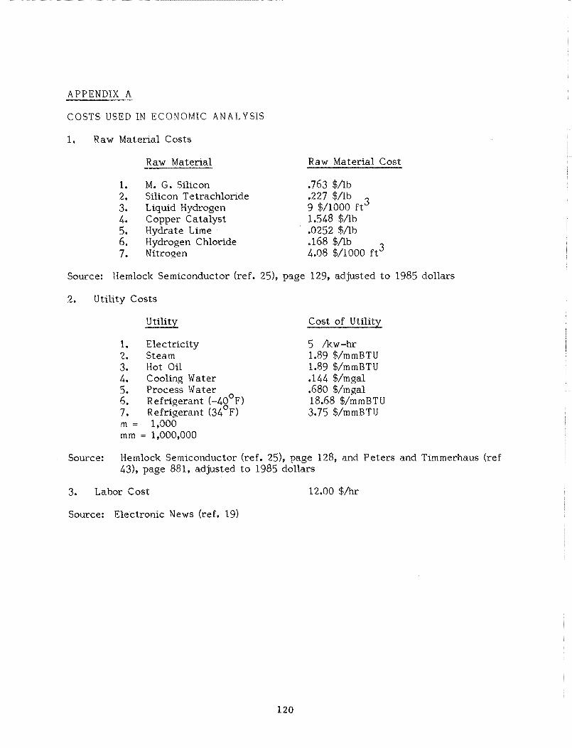
APPENDIX A
COSTS USED IN ECONOMIC ANALYSIS
1. Raw Material Costs
Raw Material Raw Material Cost
1. M, G. Silicon ,763 $Ah 2. Silicon Tetrachloride 227 $/lb 3. Liquid Hydrogen 9 $/lo00 f t 4 . Copper Catalyst 1,548 $/lb 5. Hydrate Lime ,0252 $Ab 6. Hydrogen Chloride .I68 $Ah 7. Nitroqen 4.08 $/I000 f t 3
Source: Zemlock Semiconductor (ref. 25), page 129, adjusted to 1985 dollars
2. Utility Costs
Electricity 5 /kw-hr Steam 1.89 $/mmBTU Hot Oi l 1.89 $/mmBTU Cooling Water .I44 $/rngal Process Water .680 $/mgal Refrigerant (-48'~) 18.68 $/mmBTU Refrigerant (34 F) 3.75 $/mmBT[J 1,000
= 1,000,000
Source: Hemlock Semiconductor (ref. 25), page 128, and Peters and Timmerhaus (ref 431, page 881, adjusted to 1985 dollars
3. Labor Cost 12.00 $/hr
Source: Electronic Wews (ref. 19)
P r e l . Process Design A c t i v i t y
APPENDIX B
CHECKLIST FOR CHEMICAL ENGINEERING ANALYSIS
1, Spec i fy Base Case Condit ions 1. P l a n t S i ze 2 . Product S p e c i f i c s 3. Addi t iona l Condi t ions
2 . Define Reaction Chemistry 1. Reac tan ts , Products 2 . Equi l ib r ium
3. Process Flow Diagram 1. Flow Sequence, u n i t Operat ions 2 . Process Condit ions ( T , P , e t c . ) 3. Environmental 4. Company I n t e r a c t i o n
(Technology Exchange)
4 . Ma te r i a l Balance Ca lcu l a t i ons 1. Raw Mate r i a l s 2 . Products 3 . By-Products
5 . Energy Balance Ca lcu l a t i ons 1. Heat ing 2 . Cooling 3. Addi t iona l
6 . Proper ty Data 1. Phys i ca l 2 . Thermodynamic 3. Addi t iona l
S t a t u s P r e l . Process Design A c t i v i t y
7. Equipment Design C a l c u l a t i o n s 1. Storage Vesse ls 2. Uni t Opera t ions Equipment 3 . Process Data (P, T , r a t e , e tc .) 4. Add i t i ona l
8. L i s t o f Major Process Equipment 1. S i z e 2 . Type 3. M a t e r i a l s o f Cons t ruc t ion
8a. Major Technica l Fac to r s ( P o t e n t i a l Problem Areas) 1. M a t e r i a l s Compa t ib i l i t y 2. Process Condit ion L imi t a t i ons 3 . Addi t i ona l
9. Product ion Labor Requirements 1. Process Technology 2. Product ion Volume
10. Forward f o r Economic Analys i s
0 P l an O I n P rog re s s (I Complete
S t a t u s
SHLMIZU: This morning, I presented a paper about the same sub jec t and 1 obtained quite different conclusions. Would you cement on my paper?
YAWS: Although I didn't write down complete notes on your paper, the order in which the processes was placed is about the same as in my analysis. I think you had the Hemlock Semiconductor process lower than the Union Carbide process with the Komatsu reactor, and you had the conventional Siemens process at a higher cost than Union Carbide.
SHIMIZU: Also, this morning, I compared those processes and others. In the case of silane, I compared two processes. One was the fluidized-bed reactor process, and the other was the Komatsu reactor.
YAWS: The comparison showed that the Union Carbide process with the Komatsu reactor had a lower production cost than the Siemens process.
SHIMIZU: In my estimate, the cost is about 80% that of the conventional Siemens process.
YAWS: Your table showed that the Siemens process is the most expensive. Union Carbide, using the Komatsu reactor, is second. The third is Hemlock using dichlorosilane. Those are the same results that I got. Now the numbers may be a little different, but I think our ranking orders are the same. I didn't look at as many processes as you did.
WRIGHT: You used a scaling factor for production levels from about 1500 MT/year down to 1000 MT/year. Was that a linear scaling factor? What was your justification for using that particular scaling factor?
YAWS: For normal chemical industry equipment, the factor is about 0.6, or a scaling factor which has been determined to be best for a specific type of equipment can be used. I assumed that the major cost was in reactors so that a linear factor was used for additional reactors.
PRINCE: Did you make the calculations for the Union Carbide process with the fluidized-bed reactor?
YAWS: No. That was not part of this study. The calculations were for the Union carbide process operating with Komatsu deposition reactors.
AULICH: Your calculations were for 1000 MT/year. Since 1000 MT/year capacity plants are not needed now for the photovoltaic industry, what is the analysis of the cost of these processes if smaller units of about 200 MT/year are used?
YAWS: Smaller plants would result in higher costs. Someone would have to do a study to get the answers. I can't respond to your question now, because I haven't done the analysis, but it can be done.