surface micromachining - illinois liu/liu_files/changli… · • most common surface...
TRANSCRIPT

MASSUIUC
Chang Liu
Surface Micromachining
Chang LiuMicro Actuators, Sensors, Systems Group
University of Illinois at Urbana-Champaign

MASSUIUC
Chang Liu
Outline• Definition of surface micromachining• Most common surface micromachining materials - polysilicon
and silicon oxide– LPCVD deposition of polysilicon, silicon nitride, and oxide– plasma etching for patterning structural layer– micromachined hinges - fabrication process and assembly technique– micromachined dimples and scratch drive actuators
• Other sacrificial processing systems– metal sacrificial layer, plastics materials, etc.
• Stiction and anti-stiction solutions• Multi User MEMS Process (MUMPS)
– process definition and layer naming conventions

MASSUIUC
Chang Liu
Basic Sacrificial Layer Processing• Step 1: Deposition of sacrificial layer• Step 2: patterning of the sacrificial layer• Step 3: deposit structural layer (conformal deposition)• Step 4: liquid phase removal of sacrificial layer• Step 5: removal of liquid - drying.
Sacrificial
wet etching drying

MASSUIUC
Chang Liu
Surface Micromachined Inductor
• Air bridge can be formed using sacrificial etching.

MASSUIUC
Chang Liu
Typical Device Realized by Surface Micromachining
• Etch holes are required to reduce the time for removingsacrificial layer underneath large-area structures.

MASSUIUC
Chang Liu
Inductor - By Lucent Technologies

MASSUIUC
Chang Liu
Surface Micromachined, Out of Plane Structures

MASSUIUC
Chang Liu
Hinges
• Used in micro optics component assembly.

MASSUIUC
Chang Liu
Hinge Fabrication• Step 1: deposition of
sacrificial layer.• Step 2: deposition of
structural layer.• Step 3: deposition of second
sacrificial layer.• Step 4: etching anchor to the
substrate.• Step 5: deposition of second
structural layer.• Step 6: patterning of second
structural layer• Step 7: Etch away all
sacrificial layer to releasethe first structural layer.

MASSUIUC
Chang Liu
LPCVD Process• Temperature range 500-800 degrees• Pressure range 200 - 400 mtorr (1 torr = 1/760 ATM)• Gas mixture: typically 2-3 gas mixture• Particle free environment to prevent defects on surface (pin
holes)

MASSUIUC
Chang Liu
A Laboratory LPCVD Machine

MASSUIUC
Chang Liu
LPCVD Recipes for Silicon Nitride, Polysilicon, andOxide
• Polycrystalline silicon– Polysilicon is deposited at around 580-620 oC and can withstand more
than 1000 oC temperature. The deposition is conducted by decomposingsilane (SiH4) under high temperature and vacuum (SiH4> Si+2H2).
– Polysilicon is used extensively in IC - transistor gate• Silicon nitride
– Silicon nitride is nonconducting and has tensile intrinsic stress on top ofsilicon substrates. It is deposited at around 800 oC by reacting silane(SiH4) or dichlorosilane (SiCl2H2) with ammonia (NH3) - SiH4+NH3 ->SixNy+ H.
• Silicon oxide– The PSG is knows to reflow under high temperature (e.g. above 900 oC); it
is deposited under relatively low temperature, e.g. 500 oC by reactingsilane with oxygen (SiH4+O2-> SiO2+2H2). PSG can be deposited on topof Al metallization.
– Silicon oxide is used for sealing IC circuits after processing.– The etch rate of HF on oxide is a function of doping concentration.
MASSUIUC
Chang Liu
Other Structural or Sacrificial Materials• Structural layers
– evaporated and sputtered metals such as Gold, Copper– electroplated metal (such as NiFe)– plastic material (CVD plastic)– silicon (such as epitaxy silicon or top silicon in SOI wafer)
• Sacrificial layers– photoresist, polyimide, and other organic materials– copper
• copper can be electroplated or evaporated, and is relativelyinexpensive.
– Oxide by plasma enhanced chemical vapor deposition (PECVD)• PECVD is done at lower temperature, with lower quality. It is
generally undoped.– Thermally grown oxide
• relatively low etch rate in HF.– Silicon or polysilicon
• removed by gas phase silicon etching

MASSUIUC
Chang Liu
Metal Sacrificial Layers
copper (9µm each)
Permalloy(>20µm)
PR 4620(10µm each)Aluminum
(0.3µm)

MASSUIUC
Chang Liu
Out Of Plane Devices

MASSUIUC
Chang Liu
A PECVD Machine
Reaction chamber
RFplasmagenerator
Processing gases

MASSUIUC
Chang Liu
Electroplating• Electroplating
processdescription
MASSUIUC
Chang Liu
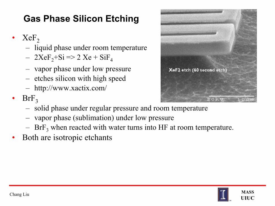
Gas Phase Silicon Etching
• XeF2– liquid phase under room temperature– 2XeF2+Si => 2 Xe + SiF4
– vapor phase under low pressure– etches silicon with high speed– http://www.xactix.com/
• BrF3– solid phase under regular pressure and room temperature– vapor phase (sublimation) under low pressure– BrF3 when reacted with water turns into HF at room temperature.
• Both are isotropic etchants

MASSUIUC
Chang Liu
Organic Sacrificial Layer
• Photoresist– etching by plasma etching (limited lateral etch extent)– or by organic solvents (acetone or alcohol)
• Polyimide– etching by organic solvents
• Advantage– extremely low temperature process– easy to find structural solutions with good selectivity
• Disadvantage– many structural layers such as LPCVD are not compatible.– Metal evaporation is also associated with high temperature metal
particles, so it is not completely compatible and caution must beused.

MASSUIUC
Chang Liu
Criteria for Selecting Materials and EtchingSolutions
• Selectivity– etch rate on structural layer/etch rate on sacrificial layer must be high.
• Etch rate– rapid etching rate on sacrificial layer to reduce etching time
• Deposition temperature– in certain applications, it is required that the overall processing
temperature be low (e.g. integration with CMOS, integration withbiological materials)
• Intrinsic stress of structural layer– to remain flat after release, the structural layer must have low stress
• Surface smoothness– important for optical applications
• Long term stability
MASSUIUC
Chang Liu
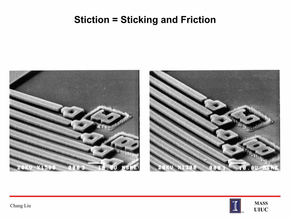
Stiction = Sticking and Friction

MASSUIUC
Chang Liu
Origin of Stiction
• As the liquidsolution graduallyvaporizes, thetrapped liquid exertsurface tensionforce on themicrostructure,pulling the devicedown.
• Surfaces can formpermanent bond bymolecule forceswhen they areclose.

MASSUIUC
Chang Liu
Antistiction Method I - Active Actuation Method
• Use magnetic actuationto pull structures awayform the surface– reduced surface
tension length of arm
• Limitations– only works for
structures withmagnetic material.

MASSUIUC
Chang Liu
Antistiction Method II -Organic Pillar
• Use organic pillar to support thestructure during the liquid removal.
• The organic pillar is removed byoxygen plasma etching.

MASSUIUC
Chang Liu
Antistiction Drying Method III - Phase Change Release MethodSupercritical CO2 Drying
• Avoid surface tension by relaying on phasechange with less surface tension than water-vapor.
• * p. 128-129• Supercritical state: temp > 31.1 oC and
pressure > 72.8 atm.• Step 1: change water with methanol• Step 2: change methanol with liquid carbon
dioxide (room temperature and 1200 psi)• Step 3: content heated to 35 oC and the carbon
dioxide is vented.
• Free-standing cantilever beams upto 850 µmcan stay released.
MASSUIUC
Chang Liu
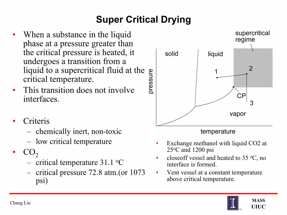
Super Critical Drying• When a substance in the liquid
phase at a pressure greater thanthe critical pressure is heated, itundergoes a transition from aliquid to a supercritical fluid at thecritical temperature.
• This transition does not involveinterfaces.
• Criteris– chemically inert, non-toxic– low critical temperature
• CO2– critical temperature 31.1 oC– critical pressure 72.8 atm.(or 1073
psi)
• Exchange methanol with liquid CO2 at25oC and 1200 psi
• closeoff vessel and heated to 35 oC, nointerface is formed.
• Vent vessel at a constant temperatureabove critical temperature.
MASSUIUC
Chang Liu
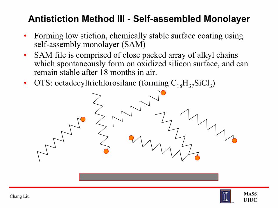
Antistiction Method III - Self-assembled Monolayer• Forming low stiction, chemically stable surface coating using
self-assembly monolayer (SAM)• SAM file is comprised of close packed array of alkyl chains
which spontaneously form on oxidized silicon surface, and canremain stable after 18 months in air.
• OTS: octadecyltrichlorosilane (forming C18H37SiCl3)

MASSUIUC
Chang Liu
Result of SAM Assembly
• Surface oxidation: H2O2 soak• SAM formation
– isopropanol alcohol rinse– CCl4 rinse– OTS solution– CCl4 rinse
MASSUIUC
Chang Liu
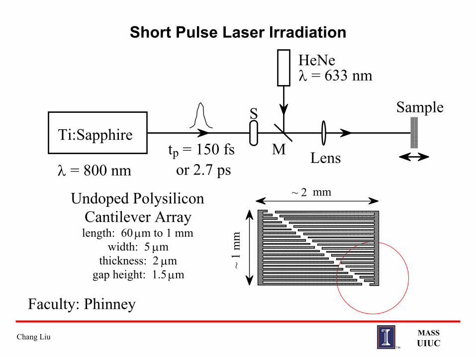
Short Pulse Laser Irradiation
λ = 800 nmtp = 150 fs or 2.7 ps
Ti:Sapphire
Sample
HeNeλ = 633 nm
S
M Lens
Undoped Polysilicon Cantilever Arraylength: 60 µm to 1 mm
width: 5 µmthickness: 2 µm
gap height: 1.5 µm
~ 1
mm
~ 2 mm
Faculty: Phinney