10ge presentation - tektronixdownload.tek.com/document/3-10ge-kr_presentation.pdf · common mode...
TRANSCRIPT

10GE Presentation
Presented by Eric

Introduction
• For a system backplane, these include:
• 1. 10 Gb/s eye of only 100 ps period, making each picosecond of eye closure from jitter a significant issue.
• 2. Frequency dependent channel loss causing significant dispersion, often tackled through the use of pre-emphasis and equalization.
• IEEE Standard 802.3ap-2007 (10GBASE-KR, or ‘KR’) compliance testing includes both physical layer and protocol components.

Backplane Overview
A representation of a backplane highlights the many sources that contribute to
overall channel loss between the two transceiver chips

10GBASE-KR Testing Overview
Block diagram showing test points TP1 and TP43

KR Transmitter Compliance Test Specifications
• Signaling Speed • Differential pk-pk Max. Amplitude • Differential pk-pk Amplitude (Tx disabled) • Common Mode Voltage • Differential Output Return Loss • Common Mode Output Return Loss • Output Transition Time • Transmit Jitter • Transmit Waveform Requirements (Mask Test)
Compliance testing at test point TP1
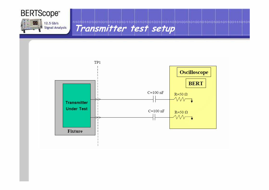
Transmitter test setup

Signaling Speed
Specification: 10.3125 Gbps ±100 ppm (10.31147 Gbps to 10.31353 Gbps)
Differential Max Amplitude Specification: ≤ 1200 mV pk-pk, with a 1010 pattern
Differential Amplitude (Tx disabled)
Specification: ≤ 30 mV pk-pk, with a 1010 pattern
Common Mode Voltage
Specification: 0 to 1.9 V DC
Common mode voltage measurements setup
The common mode voltage is the voltage offset from zero of
the transmitter module’s power supply common. Common
mode voltage should be measured using a fixture such as the
one shown in Figure 6 and is typically measured using a
digital multi-meter (DMM).

Differential Output Return Loss
Specification:
RL(f)≥ 9 for 50 MHz ≤ f < 2500 MHz
RL(f)≥ 9-12log10(f/2500 MHz) for 2500 MHz ≤ f ≤ 7500 MHz
Reference impedance is 100 Ω for differential output return loss measurements. Differential
output return loss is a measure of the match at the output of the device. It measures the
difference between the differential incident signal and the differential signal reflected back to
the source. Differential output return loss is typically measured with a vector network analyzer
Common Mode Output Return Loss
Specification:
RL(f)≥ 6 for 50 MHz ≤ f < 2500 MHz
RL(f)≥ 6-12log10(f/2500 MHz) for 2500 MHz ≤ f ≤ 7500 MHz
Reference impedance is 25 Ω for common mode output return loss measurements. Common
mode output return loss is a measure of the match at the output of the device. It measures the
difference between the common model incident signal and the common model signal reflected
back to the source. Common mode output return loss is typically measured with a vector
network analyzer
Equations 72-4 and 72-5, IEEE Std 802.3ap
Equations 72-6 and 72-7, IEEE Std 802.3ap
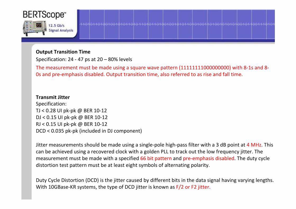
Output Transition Time
Specification: 24 - 47 ps at 20 – 80% levels
The measurement must be made using a square wave pattern (11111111000000000) with 8-1s and 8-
0s and pre-emphasis disabled. Output transition time, also referred to as rise and fall time.
Transmit Jitter
Specification:
TJ < 0.28 UI pk-pk @ BER 10-12
DJ < 0.15 UI pk-pk @ BER 10-12
RJ < 0.15 UI pk-pk @ BER 10-12
DCD < 0.035 pk-pk (included in DJ component)
Jitter measurements should be made using a single-pole high-pass filter with a 3 dB point at 4 MHz. This
can be achieved using a recovered clock with a golden PLL to track out the low frequency jitter. The
measurement must be made with a specified 66 bit pattern and pre-emphasis disabled. The duty cycle
distortion test pattern must be at least eight symbols of alternating polarity.
Duty Cycle Distortion (DCD) is the jitter caused by different bits in the data signal having varying lengths.
With 10GBase-KR systems, the type of DCD jitter is known as F/2 or F2 jitter.

Comparing DCD and F/2 Jitter
Duty Cycle Distortion (DCD) has been a term used to describe conditions where the duration of individual bits may vary. A new variant of DCD is becoming common, called F/2, or simply F2. This figure explains how F/2 differs from classic DCD.

Transmit Waveform Requirements (Mask Test)
Specification:
Transmitter waveform template (Figure 11)
Transmitter output waveform requirements (Table 1)
The transmit waveform
requirements are measured
relative to 0V with 3 tap pre-
emphasis enabled. The test
pattern required is
1111111100000000 (8-1s, 8-
0s). 32 specific voltage
measurements are performed
on the waveform as defined
by the three preceding tables.

KR Receiver Compliance Test Specifications
• Differential Input Amplitude (Maximum) • Bit Error Ratio • Receiver Coupling • Differential Input Return Loss


Signaling Speed
Specification: 10.3125 Gbps ±100 ppm (10.31147 Gbps to 10.31353 Gbps)
Differential Amplitude (Max)
Specification: 1200 mV (nominal)
Bit Error Ratio
Specification: BER better than 10E-12

Stress Parameters:

Bit Error Ratio (BER) is tested with a stress interference test
Block diagram showing receiver BER test setup
The BER test [a] requires a stressed input signal consisting of:
Pre-emphasis [b]
Frequency dependent attenuation [c]
Broadband noise (band limited) [d]
Sinusoidal and random jitter [e]
Duty cycle distortion [e]

Receiver test using link side loop back
Receiver test using internal BER testing

Pre-emphasis Requirements
Transmitter equalization communication link
Proper equalization should emulate the inverse transfer function of the test channel, right up to
the input of the receiver. This would simply be the inverse of the test channel S21 function, as
computed from the standard.

Frequency Dependent Attenuation
Test channel frequency dependent attenuation is defined to emulate the channel loss between a
transmitter and the receiver.
Test channel frequency dependent attenuation is defined to emulate the channel loss between a transmitter and the receiver.
Amax (f) = 20log10(e) x (b1f1/2 + b2f + b3f2 + b4f3) Where: b1 = 2 x 10⁻⁵ b2 = 1.1 x 10⁻¹⁰ b3 = 3.2 x 10⁻²⁰ b4 = -1.2 x 10⁻³⁰
The channel is composed of a test fixture, cables, directional couplers, and additional frequency dependent attenuation to achieve the fitted attenuation specification.
Fitted Attenuation = (measured fixture loss at 5 GHz) + (measured cable loss at 5 GHz) + (measured directional coupler loss at 5 GHz) + (added frequency dependent attenuation at 5 GHz).

Broadband Noise
Random interference is injected at the receiver end of the test channel using a broadband noise generator capable of producing white Gaussian noise.
Applied Jitter Components
Three jitter components must be added to the stress interference, sinusoidal jitter (SJ), random jitter (RJ) and duty cycle distortion (DCD). There are two types of DCD as discussed in reference [iii]. The 10GBASE-KR specification does not explicitly state, but it is assumed that the type of DCD required by the stress interference is F/2 or F2 jitter.

Differential Input Return Loss
Receiver Coupling
The KR Standard requires the receiver to be AC coupled and recommends the value to be < 100 nF to limit inrush current. However, if access is available, a capacitance meter may be used to verify a third party design.
Differential input return loss is specified to be 100 Ω differential, < -9 dB to 2.5 GHz and follows a template > 2.5 GHz. Differential return loss is typically measured with a differential Vector Network Analyzer (VNA).

Transmitter Measurement Example
The following steps show how to perform the transmitter compliance tests required by the KR Standard using the SyntheSys Research BERTScope in combination with a BERTScope Clock Recovery Unit.
Basic test setup for calibration of 10GBASE-KR transmitter compliance testing
Step 1. Configure Test Equipment for Calibration


Step 2. Configure Test Equipment for Transmitter Testing
Basic test setup for 10GBASE-KR transmitter compliance testing

Step 3. Measure Signaling Speed

Step 4. Measure Differential Amplitude

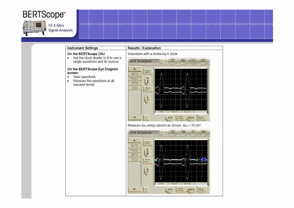
Step 5. Measure Output Transition Time
The automated rise time measurement of the BERTScope calculates rise time based on the average of the 1 and 0 values. Since the 10GBASE-KR specification requires the average value to be calculated using a subset of the time between zero crossings, the automated measurement could be slightly different from the required measurement. The BERTScope automated measurement can be used as a quick check of rise time. However, if the rise time is close to either limit, a more accurate measurement should be made using markers to manually calculate rise time. The automated measurement is shown below.


Step 6. Measure Transmit Jitter

Step 7. Measure Transmit Waveform The 32 amplitude measurements as shown in Table 5, Table 6, and Table 7 can be made with the BERTScope using cursors on an averaged waveform. The BERTScope is clocked using an internal 8:1 divider.


Receiver Measurement Example
10GBASE-KR Receiver Compliance Test Flowchart

Step 1. Configure test equipment for calibration
The following steps show how to perform the receiver compliance tests required by the KR Standard using the SyntheSys Research BERTScope in combination with a digital pre-emphasis processor, the BERTScope DPP, and a white noise source.
Basic test setup for 10GBASE-KR receiver compliance calibration

ISI Channel Characteristics
The BERTScope ISI board provides the required additional frequency dependent attenuation
using the 40” and 17” ISI traces in series is a good starting point for achieving the required additional attenuation. The total loss, excluding the fixture, can then be characterized using the BERTScope. The fixture must be characterized independently using a vector network analyzer (VNA) with proper de-embedding and added to the measured total loss of the remaining components. Using a 1010 pattern at 10.3125 Gb/s, measure the amplitude of the signal at the output of the BERTScope DPP. Next, insert the channel (fixture, cables, ISI and couplers), and measure the amplitude again. Calculate the attenuation, 20*log[(amplitude after channel)/(amplitude before channel)], then add the fixture loss.
Broadband Noise Generator A suitable broadband noise generator is the Noisewave NW10G-M, If additional amplification is required to meet the specification, a broadband linear amplifier can be added after the broadband noise generator. A suitable amplifier is the Picosecond Puslelabs 5867-107 broadband linear amplifier

Step 2. Set Data Rate and Amplitude

Step 3. Adjust the Rise Time


Step 4. Set the Pattern

Step 5. Set the Tap Values
Testing the receiver pre-emphasis control is beyond the scope of this application note. For this example, the BERTScope acts as the transmitter and equalization will be set manually by applying appropriate taps in the BERTScope DPP. The taps are set to create a filter with an inverse frequency response to that of the channel resulting in no loss to the receiver. The tap values were determined by using the frequency response plot on the DPP screen and creating an inverse frequency response to the test channel requirements stated in the KR Standard.
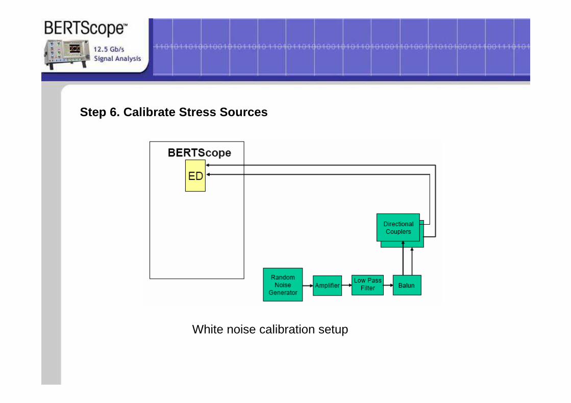
Step 6. Calibrate Stress Sources
White noise calibration setup


Step 7. Configure the Equipment for Receiver Testing
For devices with built-in BER capability, connect the equipment as shown in Figure 28 and then continue with Step 8a. For devices that support loopback, connect the equipment as shown in Figure 29 and then continue with Step 8b. For both devices, assure that the connection point entering the device is the same point that was connected to the Error Detector on the BERTScope for calibration.


Step 8a. Measure BER on a Device with Built-in BER Capability
For devices that support loopback, skip this step and continue with Step 8b.

Step 8b. Measure BER on a Device that Supports Loopback

Recommended Test Equipment