1 synchronizers for low latency clock domain transfer presented by dmitry verbitsky
Post on 19-Dec-2015
226 views
TRANSCRIPT

1
Synchronizers for Low Latency Clock Domain Transfer
Presented by Dmitry Verbitsky

2
Exactly Matched Frequencies
• All domains operate from the same clock• Skews may be arbitrary• Skew may vary due to clock jitter, power supply noise,
temperature variations, etc.

3
Rationally Related Frequencies
• Clocks are derived from a common source• Clock frequencies are rational multiples of each other

4
Closely Matched Frequencies
• Clocks are derived from independent sources
• Clock are very closely matched in frequencies

5
Arbitrary Frequencies
• Clocks are derived from independent sources• Clock can be of any arbitrary frequencies• Assume that clock frequencies are relatively stable –
satisfied by nearly all synchronous designs

6
Clock Mismatch Sources
• Difference in insertion delays between the two independent clock grids
• Reference clock distribution networks• Accumulated phase error between independent PLL sources• Primary clock distribution networks

7
Clock Mismatch Sources(2)
• PVT variations
• Variation in parameters of the wires
• Different sizing of each buffering stage
• Presence of adjacent wires and the amount of switching activities between them

8
Interfacing Synchronous and Asynchronous Systems
To achieve a sufficiently small probability of synchronization failure of a singleasynchronous input, all that is required is to allow a sufficiently long time for thesynchronizer to exit the metastable state.

9
Pipelined Synchronization
Instead of transferring W bits every 1/E seconds, one can transfer kW bits every k/E seconds in order to allow k times as much time for synchronization.

10
STARI(Self Timed At Receiver’s Input)
• Transmitter and receiver are mesochronous• If the FIFO is initialized to be roughly half full, then throughout operation, the capacity
of the FIFO remains roughly half full• The need to check overflow and underflow is avoided• Doesn’t require the absolute synchronization of purely synchronous methods• Doesn’t require the explicit flow control mechanism of purely asynchronous methods

11
MinSTARI
• FIFO reduces to latch latch-X and a latch controller• Irrespective of the phase relations between T and R, X
can always be generated in such a way as to reliably transfer data from input to output

12
Latch Controller State Diagram
• Initially starts at 0• Goes to state TR only when has seen both T
and R events• 2 possible cycles:

13
The Latch Controller Circuit

14
Transmitter Clock Event

15
Receiver Clock Event

16
Generate X

17
Reset aT and aR
18
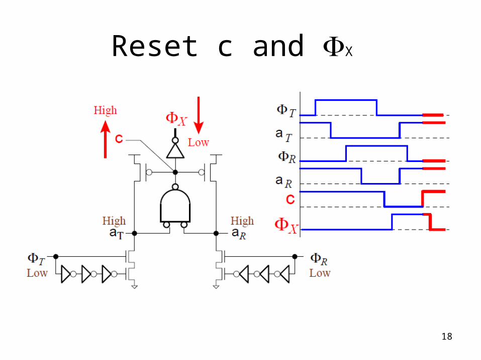
Reset c and X

19
Description of the Solution
• Low latency, high-speed interface through the integration of three major components:– Data rate matching FIFO– Pointer tracking circuit– Digital filter

20
Data rate synchronization FIFO
• Implemented as a circular queue of a given depth
• Read and write pointers are expected to exist on different clock grids
• FIFO is acting as a buffer between the two domains

21
Data rate synchronization FIFO(2)
• For mesochronous systems no need to track if FIFO full or empty
• No additional logic is required to ensure the FIFO pointers are running at similar frequences since both clocks will be derived from the same reference

22
Data rate synchronization FIFO(3)
• For heterochronous systems whose clocks are ratios of one another, a control circuit is required to reduce the frequency of the faster clock and ensure both pointers are running at the same average data rate

23
Data rate synchronization FIFO(4)
• For plesiochronous systems the allowable frequency mismatch is limited by the tracking response time of the final design implementation
• In all clocking topologies, any differences between read and write pointers clock rates must be controlled to ensure they do not exceed tracking bandwidth of the final design
24
Pointer Tracking Circuit
• By minimizing the number of unread entries in FIFO the latency is reduced
• Slow clock drift assumption relaxes the response time requirement and permits to remove the latency of the tracking circuit from the data path

25
Pointer Tracking Circuit(2)
• Possible simplifications:– No need to evaluate pointer separation on
every clock– One can choose to evaluate pointers at a
convenient time to remove ambiguity as they wrap around the FIFO structure
– Pointer information, which is delayed while being locally synchronized, can be treated as the current state of the pointer in the other domain

26
Pointer Tracking Circuit(3)
• Signal for pointer tracking is the MSB of the pointer
• Ensures that the signal will be safely captured through a simple synchronizer chain of flops in the other clock domain
• By detecting the falling edge of the MSB, one has a clear indication of when the pointer has wrapped to entry 0 of the FIFO

27
Pointer Tracking Circuit(4)
• Designed to maintain the pointers at a specific, user programmable separation
• Tracking accuracy is a function of ratios between the clock domains, the digital filter and the pointer sampling rate
• If the design is failing in a particular configuration, the pointer separation can be increased to achieve functional operation

28
Pointer tracking circuit(5)
• Relevant equations:– F = Number of FIFO entries– S = Desired/Programmed separation– E = Expected local pointer location– A = Actual local pointer location = Pointer comparison result
• If the local domain is read pointer:– E = F – S and = A – E
• If the local domain is write pointer:– E = S and = E – A

29
Tracking Logic in RdPtr Domain
In this example, E = 6 and, when the Eval signal asserts, A = 5Thus = 5-6=-1 and the pointers are detected as being too far apart.

30
Timing Diagram Detecting Pointers Are Drifting Apart

31
Pointer Adjustment
• One clock is nominally faster than anotherPtrs too close(suppress one Fast ClockPtrs too far (allow one extra Fast
Clock
• Neither clock is nominally fasterPtrs too close(suppress one clock on
the Write PointerPtrs too far (suppress one clock on
the Read Pointer

32
Digital Filter
• Reasons:– Tracking logic is susceptible to metastability
on the synchronizer chain– Data rate matching circuit may produce non-
uniform clock patterns
• Example:– Make adjustment only if in m samples, there
were n detections of the pointers too far, (or conversely too close) where n is an integer

33
Sampling Uncertainties
• By design any missed event is guaranteed to be capture on the very next clock
• This translates to one FIFO entry of uncertainty
• The other main contributor to uncertainty is the irregular duty cycle of the throttled clock

34
Uncertainty Due to Sample Jitter

35
Tracking Response Time
• F = Number of FIFO entries• S = Number of samples required by the digital
filter• = FIFO throttled data rate, typically the
clock period of the slow domain• = Maximum clock edge mismatch. The
degree of phase mismatch between the throttled clock and the data-rate clock
• = Maximum percentage of allowable clock mismatch

36
Tracking Response Time(2)
• F*S)+(F-1))*• F*S – total sample time• (F-1) – worst case latency to the first
sample

37
Tracking Response Time(3)
• Simplification : • F*S)+(F-1) F*(S+1))*100
• By pipelining the throttled clock pattern which controls the faster domains’ pointer, the equation is modified to:
F*(S+1)+P)*100

38
Tracking Response Time(4)
• Example:– 8 Entry FIFO (F)– 3 Sample Filter (S)– 1 Clock Uncertainty ()– 8 Clock Pipeline (P)or 25000 PPM

39
Further Refinements
• Looking at the pointer separation slightly earlier in time can predict a pointer collision before it actually occurs. For example, invert the clock on the synchronizer chain
• Optimization of digital filter by more accurate tracking of pointers drift to avoid pointer collision when reducing their separation

40
Conclusions
• Design effectively reduces the latency across two clock domains in systems where the clock drift is slow but unbounded in duration
• The digital nature of design allows the implementation to scale in frequency without the potential risk of self-timed circuits
• The only true constraint on its use is that the domain clock frequencies must be known prior to activating the FIFO to ensure that pointers are advancing within the bandwidth of the tracking logic

41
A Predictive Synchronizer for Periodic Clock Domains

42
Synchronizer Architecture

43
Synchronizer Overview
• Receives the two clocks and manages safe data transfer both ways
• Produces SEND and RECV control outputs to both domains, indicating when it is safe to receive and send new data on both sides, avoiding data misses and duplicates due to mismatched clock frequencies

44
Clock Conflicts Prediction
• Can be predicted in advance due to periodic nature of the two clocks
• Let’s assume we have a conflict at time zero
• The next conflict occurs when there exist some N and K such that:N*TLOCAL=K*TEXT

45
Clock Conflicts Prediction(2)
• Find the smallest such that:TLOCAL+ = M* TEXT
• (N-1)*TLOCAL = K*TEXT – TLOCAL
• (N-1)*TLOCAL = (K-M) *TEXT + • Conflict prediction is achieved by creating
a Predictive Clock which is a version of the external clock delayed by

46
Clock Conflicts Prediction(3)
• Predicted and Local clocks conflict one TLOCAL cycle before the imminent conflict of the External and Local clocks
• Sampling the input (which is affected by RxCK) is delayed by a keep-out time TKO, where TKO>dZ

47
Conflict Detector
• FF1 and FF2 effectively sample Clk2 d time after and d time before the rising edge of Clk1, respectively
• Either FF may become metastable• One half cycle of Clk1 is allotted for metastability resolution• If Clk2 has risen during the 2d detection period, the top AND gate is
enabled and Conflict output is generated

48
Computing Clock Cycle Time
• Circuit starts with minimal delay and increases (or decreases) delay until it is equal to a full cycle
• The clock divider and flip-flop provide a loop delay (of two local clock cycles) • Time resolution of Conflict detector must be larger than adjustment step• Once the lower delay line has converted to TLOCAL, its programming code is
copied to the upper delay line

49
Computing Clock Cycle Time(2)
• The TLOCAL unit safely computes cycle time with precision dL
• DLL convergence time is: / 2LOCAL LOCALT q T

50
Clock Predictor
• “Predicted clock” output provides a copy of external clock, delayed by , one local cycle time in advance
• Loop delay must be the maximum of the two clock cycles

51
Rate Reducer
• The delay introduced by Rate Reducer between successive adjustments is 4TLOCAL+4TEXT
• Total tuning time of Programmable Delay 1 is:
/4EXTERNAL LOCAL
LOCAL EXTERNAL
K N T TT T
q

52
Clock Predictor Precision
• Clock Predictor safely generates a delayed version of the external clock that periodically precedes its original version by TLOCAL with precision ( )dL dP

53
Conflict Prevention Circuit
• The dC-conflict detector produces the Keep-Out signal upon a dC conflict of the local and predicted clocks
• The Clock Select circuit produces RxCK depending on Keep-Out• RxCK is either the original local clock (when there is no predicted
conflict) or the TKO delayed local clock (when a conflict is predicted)

54
Prediction Timing Diagram
2
2 1
1
11
| |
( )
| ( ) |
| || |
L E
L L LOCAL
E P LOCAL
L LOCAL P LOCAL
L PL P
t t dZ
t t T
t t T dL dP
t T t T dL dP dZ
t t dZ dL dPt t dC
dC dZ dL dP

55
TKO constraint
• Definition:– R: The rising edge event of RxCK– D: Event R when Keep-Out = 1
• Theorem:– If L1 and P occur within dC time of each other,
then D and E are safely separated by at least dZ of each other

56
TKO constraint(2)
• Proof:
1| |PLt t dC
Need to confirm that: | |D Et t dZ
By definition: 2D L KOt t T
1
1
1
1
| ( ( )) |
| |
| |
( ) 2
L LOCAL KO P LOCAL
L KO P
L KO P
KO L P KO
t T T t T dL dP dZ
t T t dZ dL dP
t T t dC
T dC t t T dC

57
Avoiding Misses and Duplicates

58
Duplicate and Miss Control Circuit

59
Duplicate and Miss Control Circuit(2)

60
Conclusions
• Synchronizer takes advantage of periodic nature of clocks in order to predict potential conflicts in advance, and to conditionally employ an input sampling delay to avoid such conflicts
• Adjusts automatically to wide range of clock frequencies
• Avoids sampling duplicate data or missing any input

61
References• Wade L. Williams, Philip E. Madrid, Scott C. Johnson, "Low Latency Clock Domain
Transfer for Simultaneously Mesochronous, Plesiochronous and Heterochronous Interfaces," async, pp.196-204, 13th IEEE International Symposium on Asynchronous Circuits and Systems (ASYNC'07), 2007
• J.N. Seizovic, “Pipeline Synchronization”, Proceedings of the 1st International Symposium on Advanced Research in Asynchronous Circuits and Systems, pp. 87-96, 1994.
• A. Chakraborty and M.R. Greenstreet, “Efficient Self-Timed Interfaces for Crossing Clock Domains,” Proceedings 9th IEEE International Symposium on Asynchronous Circuits and Systems (ASYNC’03), pp. 78-88, 2003.
• U. Frank, T. Kapschitz and R. Ginosar, “A Predictive Synchronizer for Periodic Clock Domains,” J. Formal Methods in System Design (special issue on Formal Methods for Globally Asynchronous Locally Synchronous Design), 28(2):171-186, 2006