adapting synchronizers to the effects of on-chip variability david kinniment alex yakovlev jun zhou...
Post on 21-Dec-2015
220 views
TRANSCRIPT
Adapting Synchronizers to the Effectsof On-Chip Variability
David KinnimentAlex Yakovlev
Jun ZhouGordon Russell
Presented by Dmitry Verbitsky
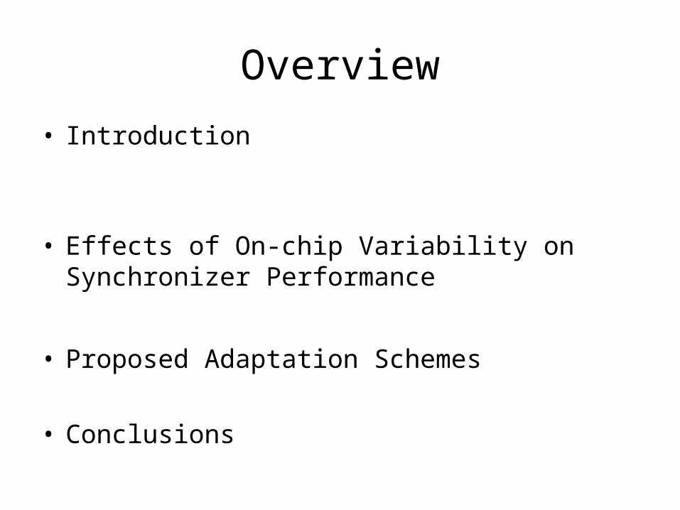
Overview
• Introduction
• Effects of On-chip Variability on Synchronizer Performance
• Proposed Adaptation Schemes
• Conclusions
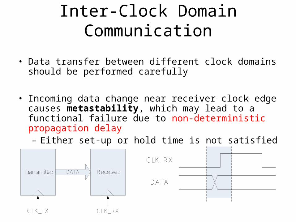
Inter-Clock Domain Communication
• Data transfer between different clock domains should be performed carefully
• Incoming data change near receiver clock edge causes metastability, which may lead to a functional failure due to non-deterministic propagation delay– Either set-up or hold time is not satisfied
Transmitter ReceiverDATA
CLK_TX CLK_RX
CLK_RX
DATA
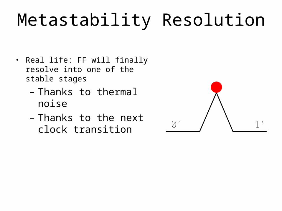
Metastability Resolution
• Real life: FF will finally resolve into one of the stable stages
– Thanks to thermal noise– Thanks to the next clock
transition
0’ 1’
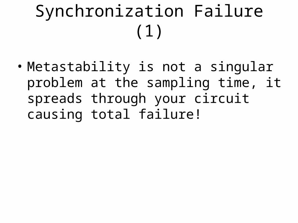
Synchronization Failure (1)
• Metastability is not a singular problem at the sampling time, it spreads through your circuit causing total failure!
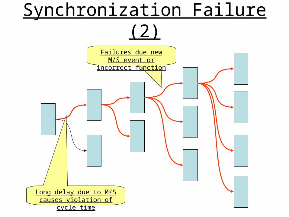
Synchronization Failure (2)
Long delay due to M/S causes violation of cycle time
Failures due new M/S event or incorrect function
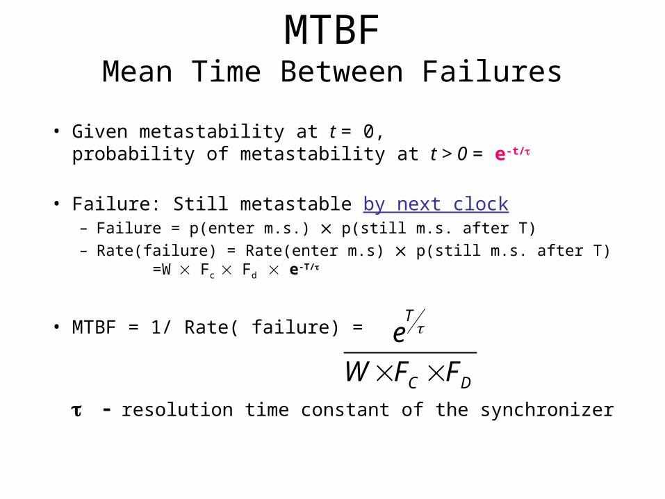
MTBFMean Time Between Failures
• Given metastability at t = 0, probability of metastability at t > 0 = e-t/
• Failure: Still metastable by next clock– Failure = p(enter m.s.) p(still m.s. after T)– Rate(failure) = Rate(enter m.s) p(still m.s. after T)
=W Fc Fd e-T/
• MTBF = 1/ Rate( failure) =
resolution time constant of the synchronizer
T
C D
e
W F F
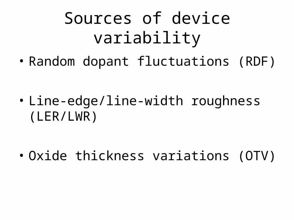
Sources of device variability
• Random dopant fluctuations (RDF)
• Line-edge/line-width roughness (LER/LWR)
• Oxide thickness variations (OTV)
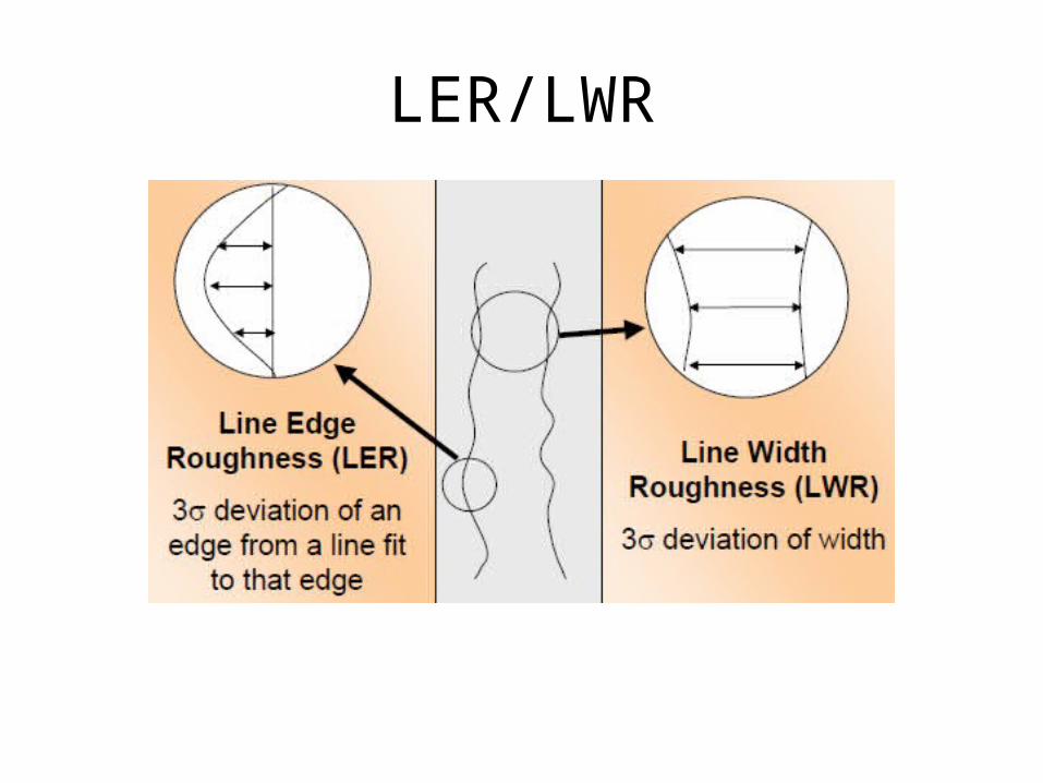
LER/LWR
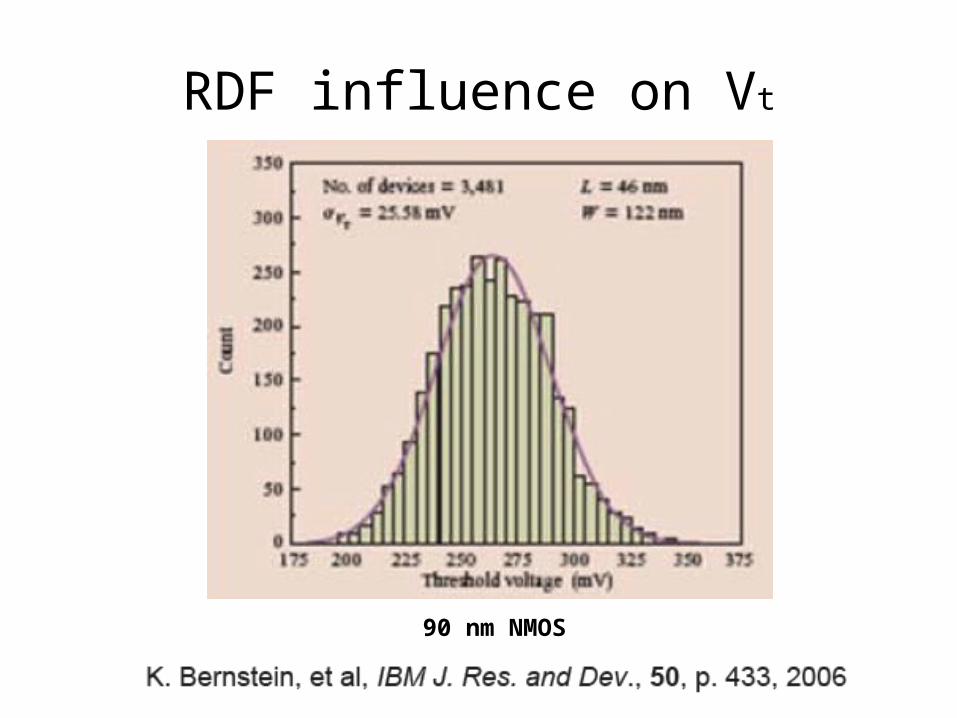
RDF influence on Vt
90 nm NMOS
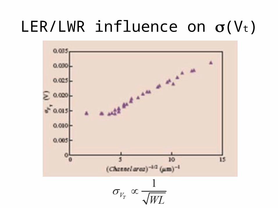
LER/LWR influence on (Vt)
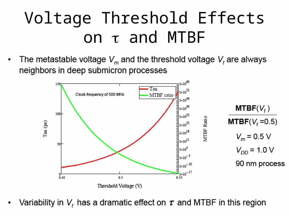
Voltage Threshold Effectson and MTBF
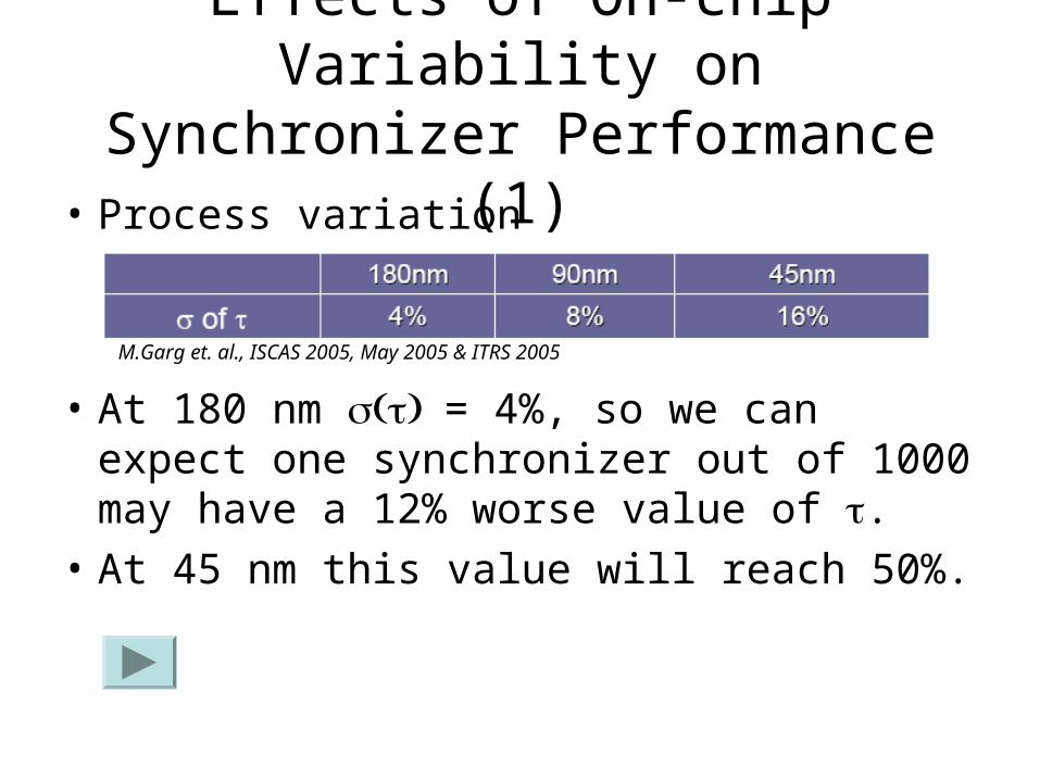
Effects of On-chip Variability onSynchronizer Performance (1)
• Process variation
• At 180 nm = 4%, so we can expect one synchronizer out of 1000 may have a 12% worse value of .
• At 45 nm this value will reach 50%.
M.Garg et. al., ISCAS 2005, May 2005 & ITRS 2005
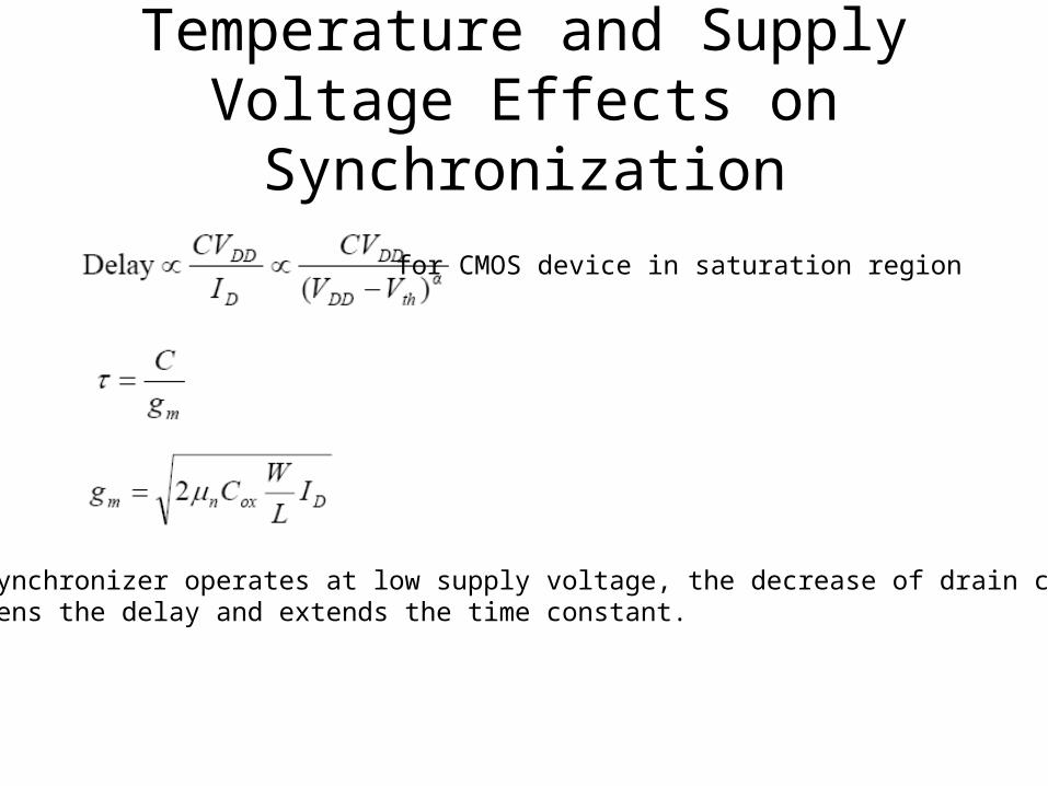
Temperature and Supply Voltage Effects on Synchronization
for CMOS device in saturation region
When synchronizer operates at low supply voltage, the decrease of drain currentlengthens the delay and extends the time constant.
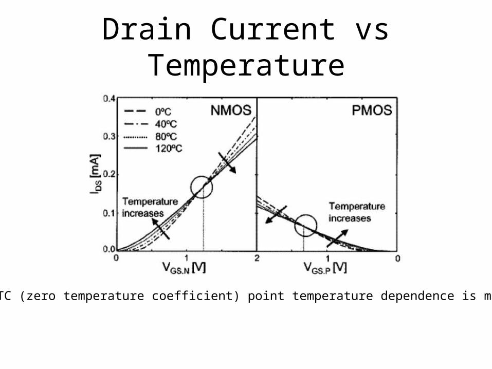
Drain Current vs Temperature
Near ZTC (zero temperature coefficient) point temperature dependence is minimized
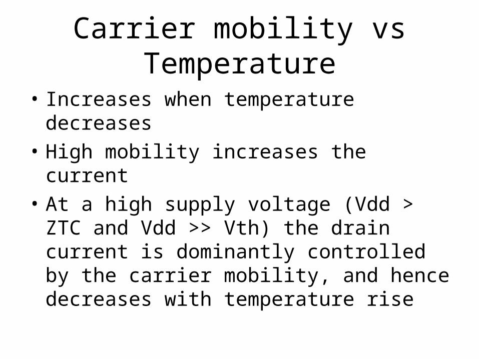
Carrier mobility vs Temperature
• Increases when temperature decreases
• High mobility increases the current
• At a high supply voltage (Vdd > ZTC and Vdd >> Vth) the drain current is dominantly controlled by the carrier mobility, and hence decreases with temperature rise

Threshold Voltage vs Temperature
• Increases when temperature decreases
• Higher Vth decreases the current
• When Vdd approaches Vth (Vdd < ZTC), Vth has a stronger effect on the drain current, and as a result the current grows with temperature rise
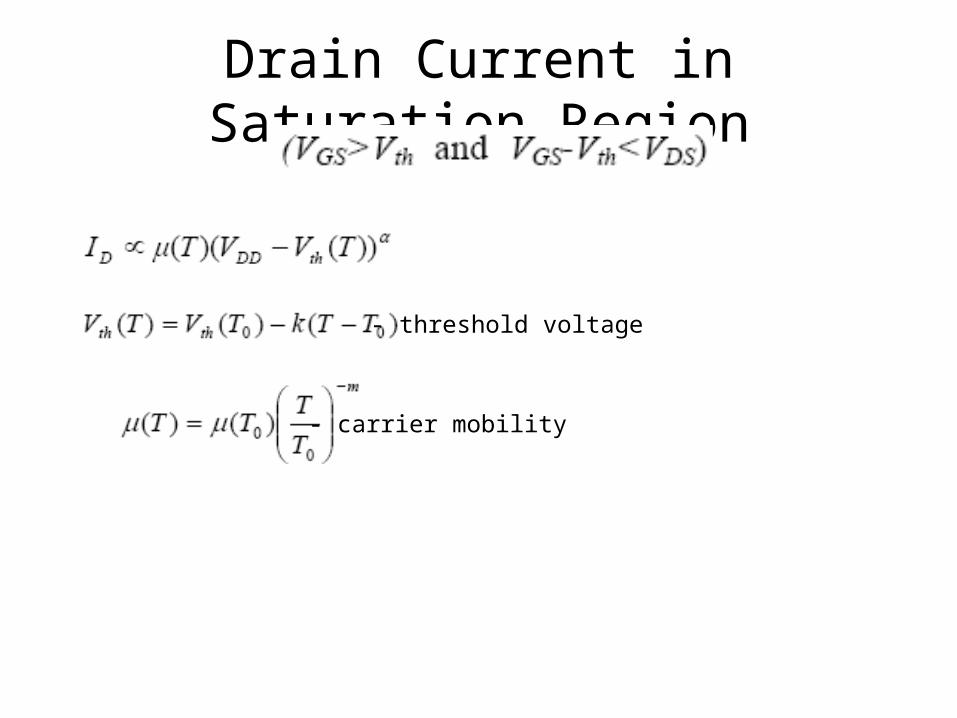
Drain Current in Saturation Region
- threshold voltage
- carrier mobility

High Vdd~ ( )D DDI t V
0 20 40 60 80 100 120
temperature
mobility
Id

Low Vdd~ ( )D thI t V
0 20 40 60 80 100 120
temperature
Vth
mobility
Id
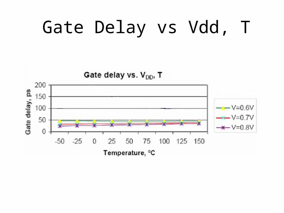
Gate Delay vs Vdd, T

vs Vdd, T

Effects of On-chip Variability onSynchronizer Performance (2)
• Voltage and Temperature variations
• Disproportional affect is observed. As a result a 50% reduction in power supply voltage may cause over 100% increase in
Simulation results of Jamb latch at 90nm
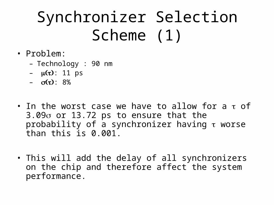
Synchronizer Selection Scheme (1)
• Problem:– Technology : 90 nm– : 11 ps– : 8%
• In the worst case we have to allow for a of 3.09 or 13.72 ps to ensure that the probability of a synchronizer having worse than this is 0.001.
• This will add the delay of all synchronizers on the chip and therefore affect the system performance.
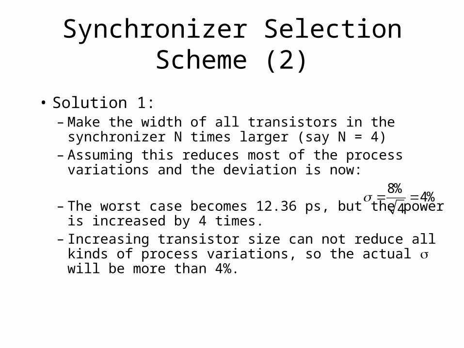
Synchronizer Selection Scheme (2)
• Solution 1:– Make the width of all transistors in the synchronizer N
times larger (say N = 4)– Assuming this reduces most of the process variations
and the deviation is now:
– The worst case becomes 12.36 ps, but the power is increased by 4 times.
– Increasing transistor size can not reduce all kinds of process variations, so the actual will be more than 4%.
8%4%
4
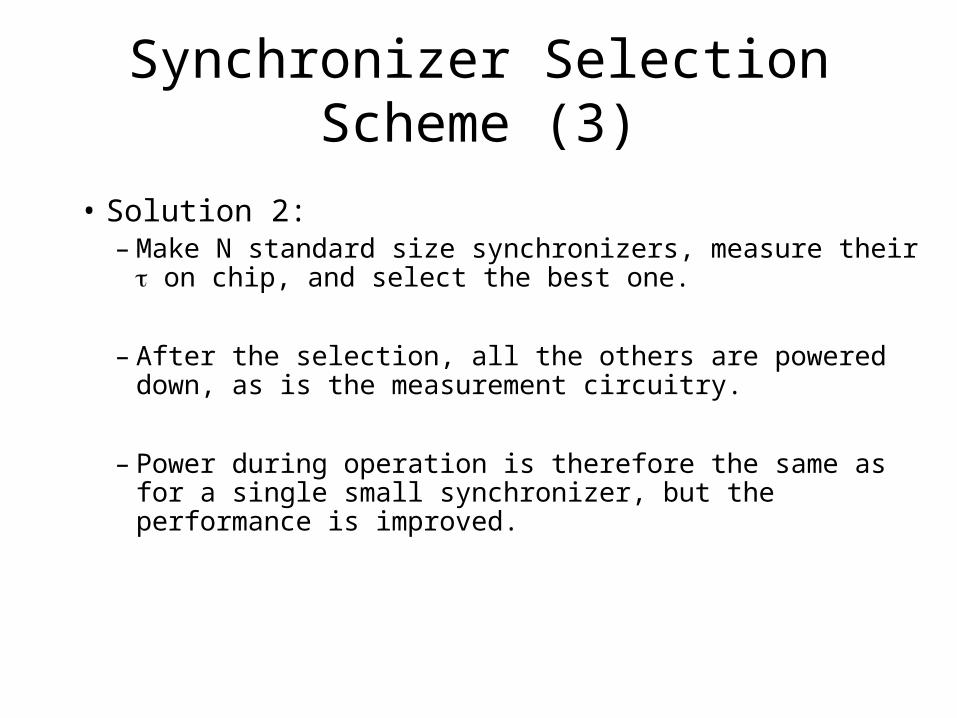
Synchronizer Selection Scheme (3)
• Solution 2:– Make N standard size synchronizers, measure their on
chip, and select the best one.
– After the selection, all the others are powered down, as is the measurement circuitry.
– Power during operation is therefore the same as for a single small synchronizer, but the performance is improved.
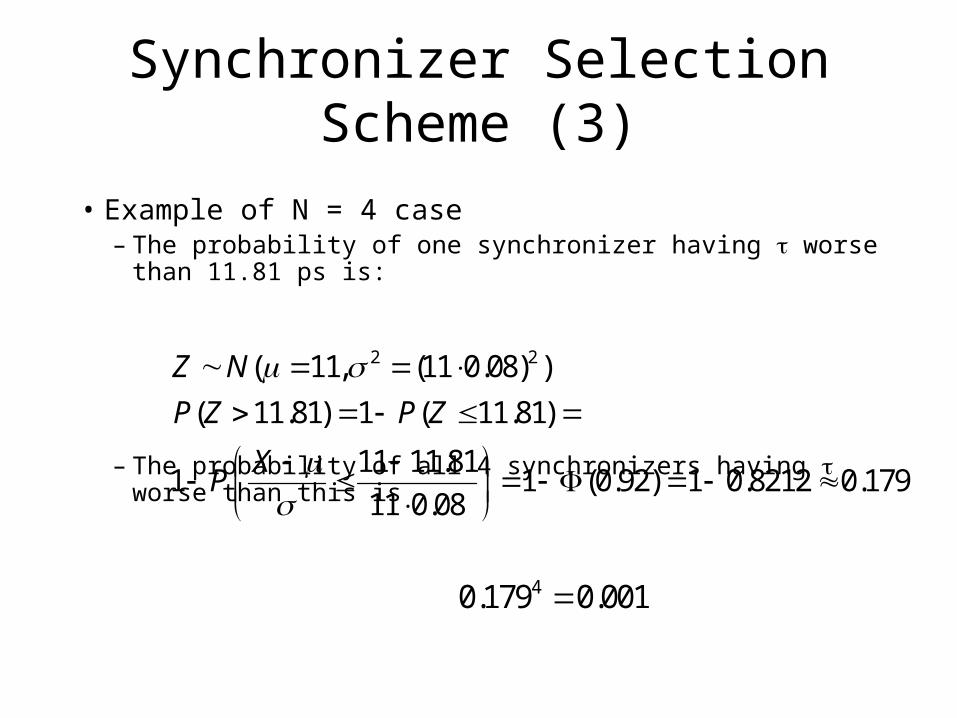
Synchronizer Selection Scheme (3)
• Example of N = 4 case– The probability of one synchronizer having worse than
11.81 ps is:
– The probability of all 4 synchronizers having worse than this is
2 2( 11, (11 0.08) )
( 11.81) 1 ( 11.81)
11 11.811 1 (0.92) 1 0.8212 0.179
11 0.08
Z N
P Z P Z
XP
40.179 0.001
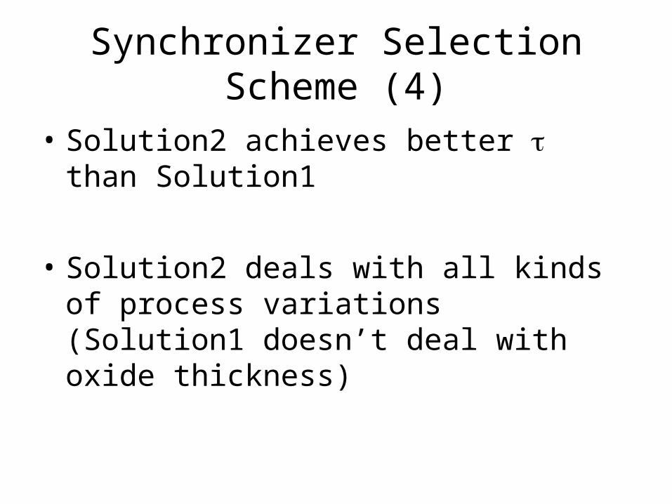
Synchronizer Selection Scheme (4)
• Solution2 achieves better than Solution1
• Solution2 deals with all kinds of process variations (Solution1 doesn’t deal with oxide thickness)
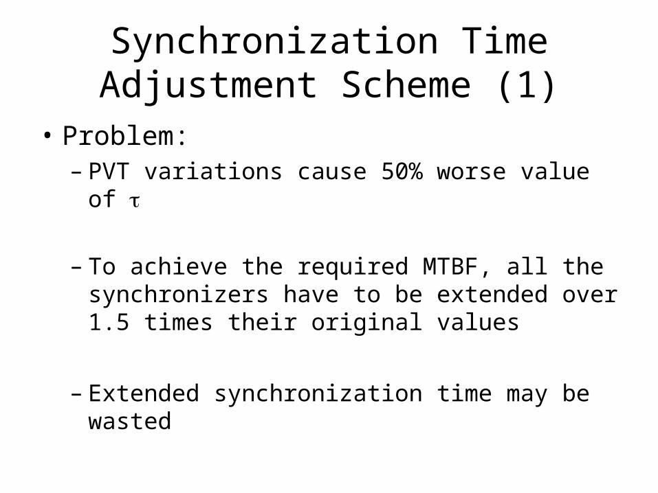
Synchronization Time Adjustment Scheme (1)
• Problem:– PVT variations cause 50% worse value of
– To achieve the required MTBF, all the synchronizers have to be extended over 1.5 times their original values
– Extended synchronization time may be wasted
Synchronization Time Adjustment Scheme (2)
• Solution:– Adjust synchronization time of each
synchronizer according to actual PVT and data rate variations to improve the system performance on the conditions that the required MTBF is met
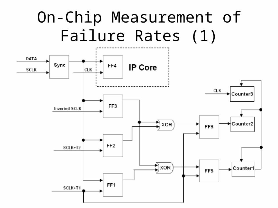
On-Chip Measurement of Failure Rates (1)
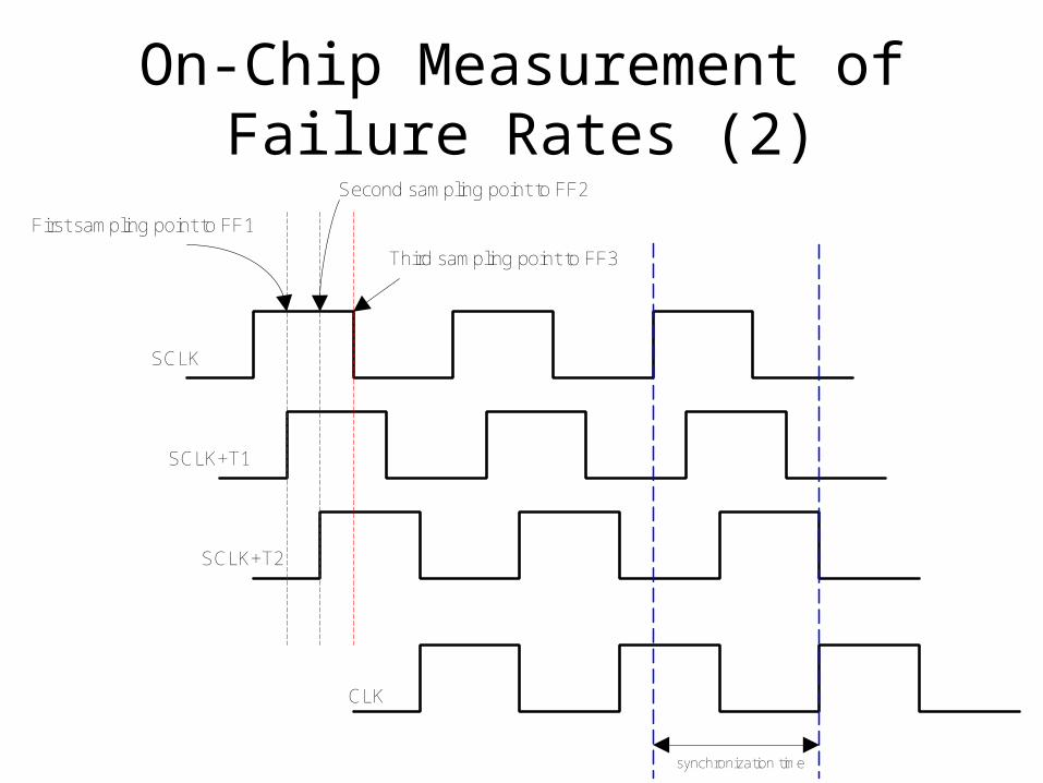
On-Chip Measurement of Failure Rates (2)
SCLK
SCLK+T1
SCLK+T2
First sampling point to FF1
Second sampling point to FF2
Third sampling point to FF3
CLK
synchronization time
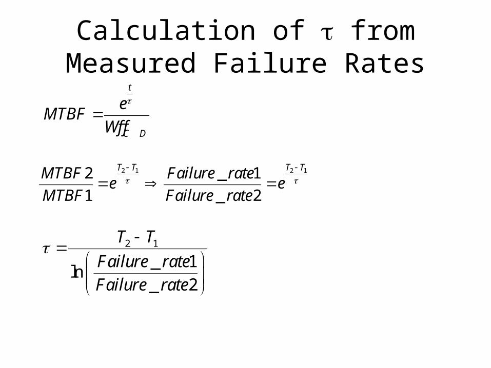
Calculation of from Measured Failure Rates
2 1 2 12 _ 1
1 _ 2
T T T TMTBF Failure ratee e
MTBF Failure rate
t
C D
eMTBF
Wf f
2 1
_ 1ln
_ 2
T T
Failure rateFailure rate
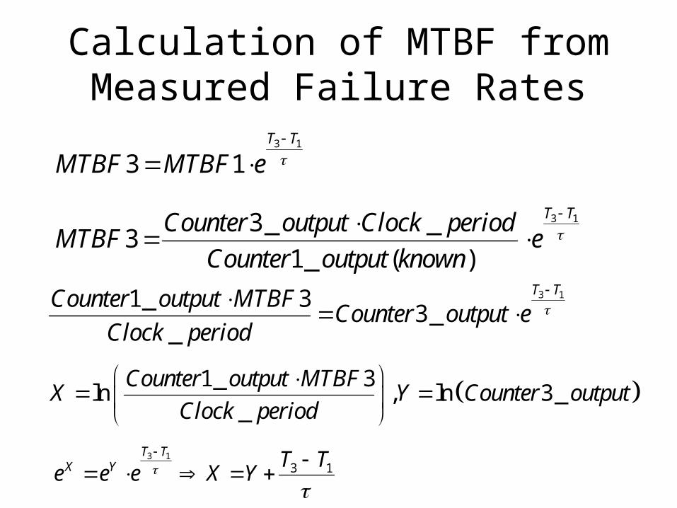
Calculation of MTBF from Measured Failure Rates
3 11_ 33_
_
T TCounter output MTBFCounter output e
Clock period
1_ 3ln , ln 3_
_
Counter output MTBFX Y Counter output
Clock period
3 1
3 1T T
MTBF MTBF e
3 13_ _3
1_ ( )
T TCounter output Clock periodMTBF e
Counter output known
3 1
3 1T T
X Y T Te e e X Y
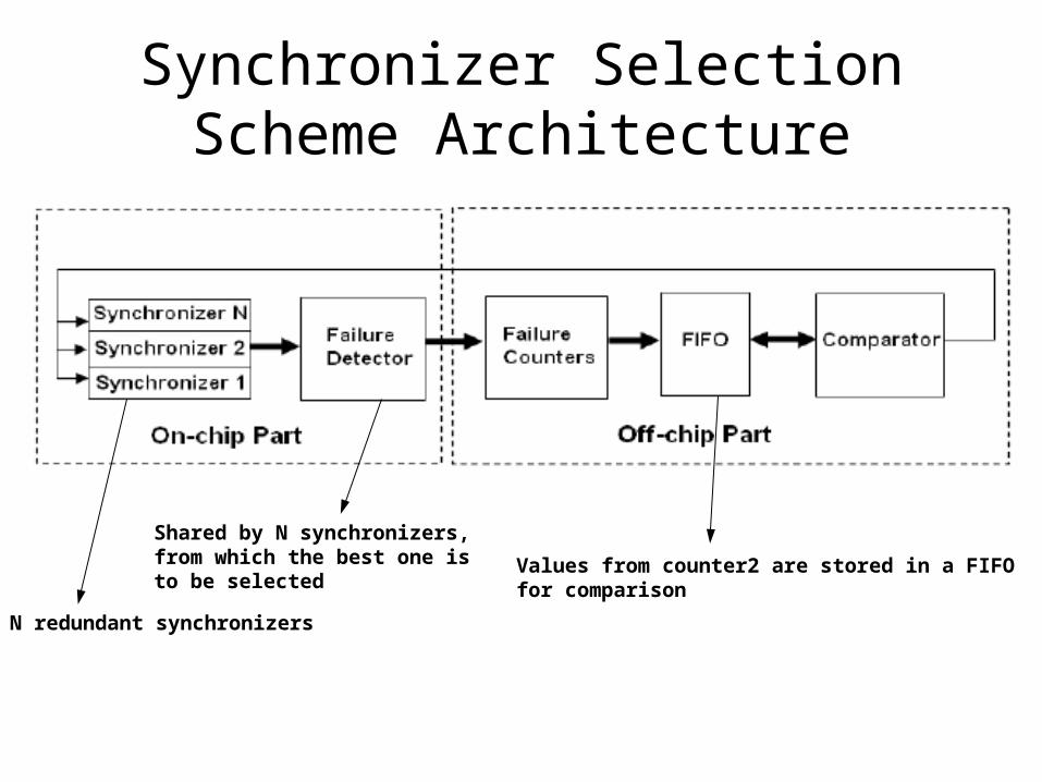
Synchronizer Selection Scheme Architecture
N redundant synchronizers
Shared by N synchronizers,from which the best one isto be selected
Values from counter2 are stored in a FIFOfor comparison
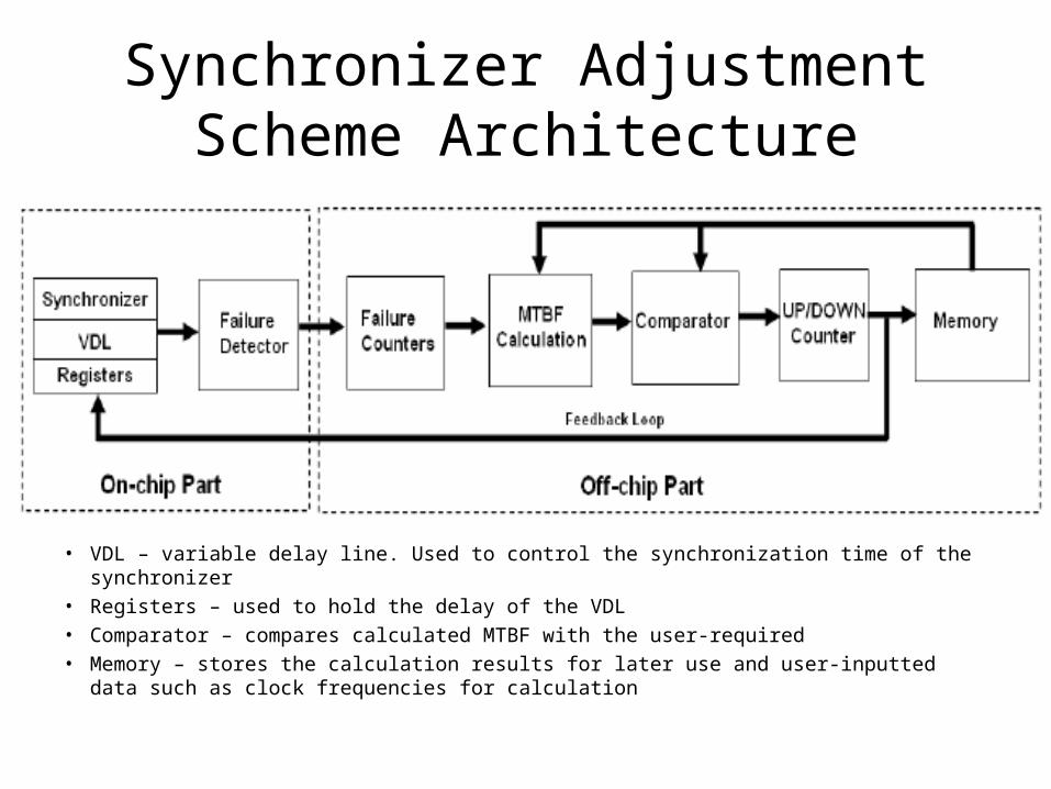
Synchronizer Adjustment Scheme Architecture
• VDL – variable delay line. Used to control the synchronization time of the synchronizer• Registers – used to hold the delay of the VDL• Comparator – compares calculated MTBF with the user-required• Memory – stores the calculation results for later use and user-inputted data such as
clock frequencies for calculation
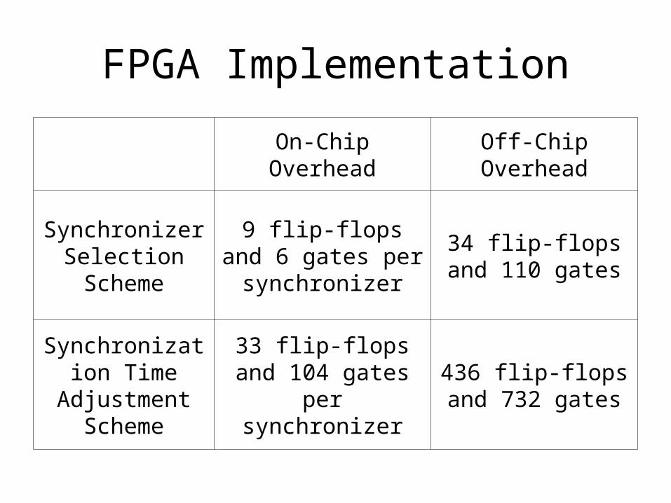
FPGA Implementation
On-Chip Overhead Off-Chip Overhead
SynchronizerSelection Scheme
9 flip-flops and 6 gates per synchronizer
34 flip-flops and 110 gates
Synchronization Time Adjustment
Scheme
33 flip-flops and 104 gates per synchronizer
436 flip-flops and 732 gates
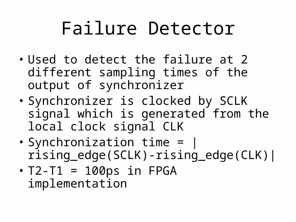
Failure Detector
• Used to detect the failure at 2 different sampling times of the output of synchronizer
• Synchronizer is clocked by SCLK signal which is generated from the local clock signal CLK
• Synchronization time = |rising_edge(SCLK)-rising_edge(CLK)|
• T2-T1 = 100ps in FPGA implementation
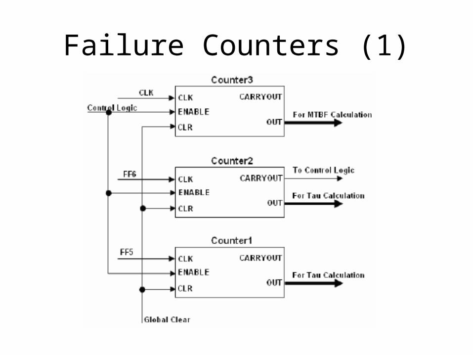
Failure Counters (1)
Failure Counters (2)
• Count the number of failures detected at different sampling times
• Counters 1 and 2 are used to count the number of failures at the sampling times SCLK+T1 and SCLK+T2
• Counter3 is used to count the number of clock cycles
• For the synchronizer selection scheme Counter3 is not needed so the hardware overhead can be further reduced
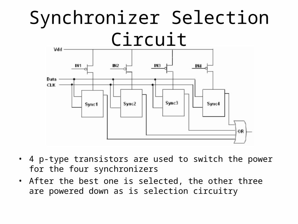
Synchronizer Selection Circuit
• 4 p-type transistors are used to switch the power for the four synchronizers
• After the best one is selected, the other three are powered down as is selection circuitry
Variable Delay Line(1)
• Usually implemented by transistor level circuits
• In FPGA can only be implemented as inverter chains. Inverters, in turn, are implemented by LUTs.
• LUT delay + wire delay > 1 ns on Spartan3• Smaller incremental delay can be
achieved by using the connection delay difference on FPGA
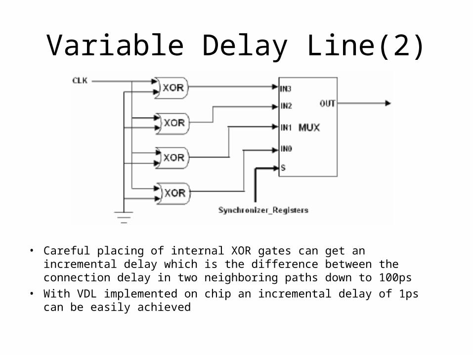
Variable Delay Line(2)
• Careful placing of internal XOR gates can get an incremental delay which is the difference between the connection delay in two neighboring paths down to 100ps
• With VDL implemented on chip an incremental delay of 1ps can be easily achieved
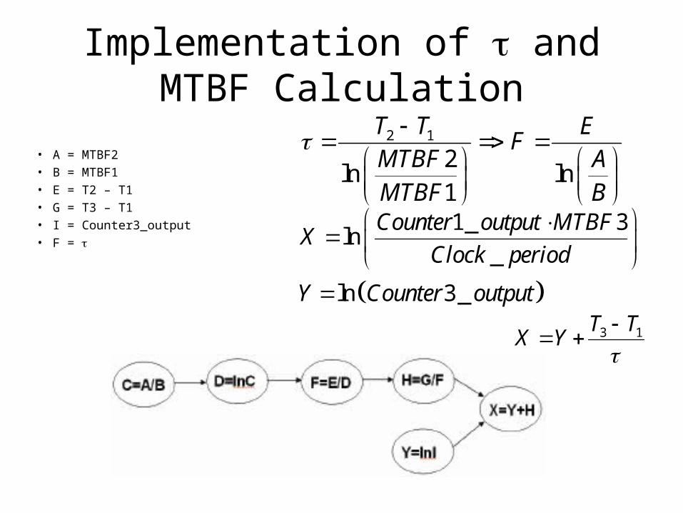
Implementation of and MTBF Calculation
2 1
2ln ln
1
T T EF
MTBF AMTBF B
• A = MTBF2• B = MTBF1• E = T2 – T1• G = T3 – T1• I = Counter3_output• F =
1_ 3ln
_
ln 3_
Counter output MTBFX
Clock period
Y Counter output
3 1T TX Y

Division Implementation
• Divider is pipelined to achieve high performance and low area• Divisor and dividend inputs are multiplexed to make it reusable• Control Counter counts the number of clock cycles used for division• Register stores divider output for later division steps
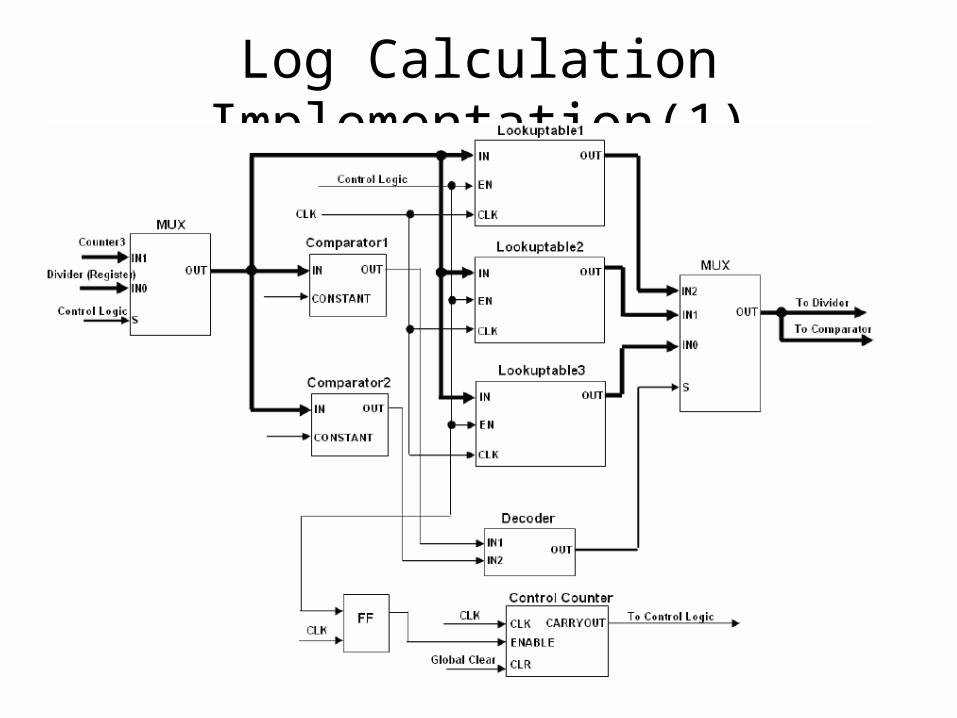
Log Calculation Implementation(1)
Log Calculation Implementation(2)
• Uses lookup tables• Due to possibly large values it is
impossible to build a full log LUT• Different resolutions can be used for
calculating different values (high resolution for small values, and low – for larger ones)
• 3 LUTs are used to provide an accuracy of 2 decimals, which leads to an error of 1% in calculated MTBF
Hardware Saving
• 80% of on-chip overhead goes on VDL implementation on FPGA
• When implemented on chip using transistors the overhead will be reduced by 50%
• Off-chip part can also be reduced by lowering the calculation accuracy
Application of 2 Schemes (1)
• Synchronizer selection scheme is aimed at improving synchronizer performance subject to process variation
• It only needs to operate once when setting up the chip since the process variation is fixed when the chip is fabricated
• After the selection, power consumption is the same as of single synchronizer, because all redundant modules are powered down
• The scheme has a small overhead and can be entirely put on chip
Application of 2 Schemes (2)
• Synchronization time adjustment scheme is used to deal with PVT and data rate variations
• Consumes relatively large amount of power and hardware
• Only needs to operate once when deals with process or fixed Vdd variations. Can be powered down after all
• When deals with frequent data rate or power variations, the scheme needs to be put entirely on chip and operate frequently
• Power consumption can be reduced by reducing hardware complexity and adjustment rate
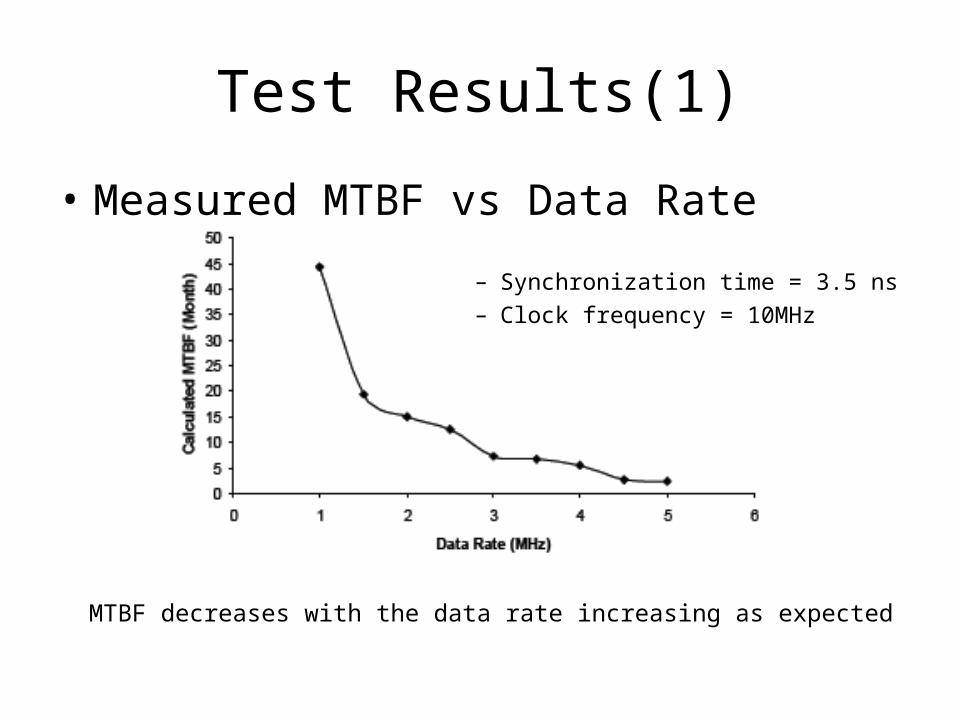
Test Results(1)
• Measured MTBF vs Data Rate
– Synchronization time = 3.5 ns– Clock frequency = 10MHz
MTBF decreases with the data rate increasing as expected
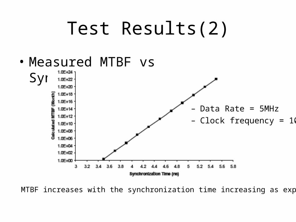
Test Results(2)
• Measured MTBF vs Synchronization Time
– Data Rate = 5MHz– Clock frequency = 10MHz
MTBF increases with the synchronization time increasing as expected
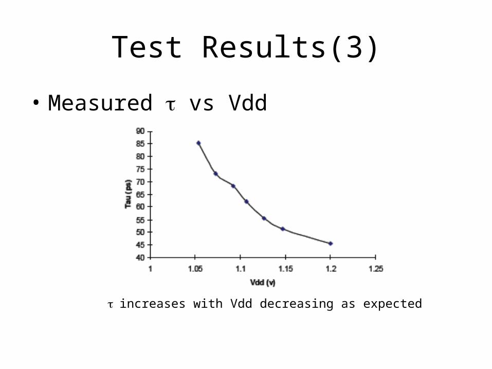
Test Results(3)
• Measured vs Vdd
increases with Vdd decreasing as expected
Conclusions
• Two adaptation schemes have been proposed to reduce the effects of on-chip variability on synchronizers. They both were implemented on Xilinx’s FGPA Spartan3
• Synchronizer selection scheme deals with process variations, has a small overhead and can be put entirely on chip
• Synchronization time adjustment scheme deals with PVT and data rate variations. It has a relatively large overhead, which can be reduced by lowering the calculation accuracy of MTBF.
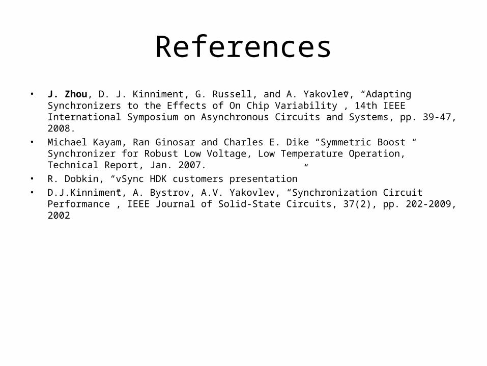
References• J. Zhou, D. J. Kinniment, G. Russell, and A. Yakovlev, “Adapting Synchronizers to the Effects of
On Chip Variability”, 14th IEEE International Symposium on Asynchronous Circuits and Systems, pp. 39-47, 2008.
• Michael Kayam, Ran Ginosar and Charles E. Dike “Symmetric Boost Synchronizer for Robust Low Voltage, Low Temperature Operation,” Technical Report, Jan. 2007.
• R. Dobkin, “vSync HDK customers presentation”
• D.J.Kinniment, A. Bystrov, A.V. Yakovlev, “Synchronization Circuit Performance”, IEEE Journal of Solid-State Circuits, 37(2), pp. 202-2009, 2002

The End
Questions?

Rules for Normally Distributed Data
• If a data distribution is approximately normal, then:– 68% of the data values are within – 95% of the data values are within – 99.7% of the data values are within