Статья nano-magnetism
TRANSCRIPT

NPL Report DEM-TQD-002
NPL REPORT DEM-TQD-002 Metrological challenges of nanomagnetism Olga Kazakova Carol Webster Alexander Tzalenchuk NOT RESTRICTED OCTOBER 2005
National Physical Laboratory | Hampton Road | Teddington | Middlesex | United Kingdom | TW11 0LW
Switchboard 020 8977 3222 | NPL Helpline 020 8943 6880 | Fax 020 8943 6458 | www.npl.co.uk


NPL Report DEM-TQD-002
Metrological Challenges of Nanomagnetism
Olga Kazakova Carol Webster
Alexander Tzalenchuk DEM
ABSTRACT This is a study of the leading edge science, key industrial developments and international position in nanomagnetism. It outlines a roadmap in this area for NPL and sets out the scope for future work to be considered in the formulation of the next Quantum Metrology Program.
NPL Report DEM-TQD-002
© Crown copyright 2005 Reproduced with the permission of the Controller of HMSO
and Queen's Printer for Scotland
ISSN 1744-0491
National Physical Laboratory Hampton Road, Teddington, Middlesex, TW11 0LW
Extracts from this report may be reproduced provided the source is acknowledged and the extract is not taken out of context.
Approved on behalf of the Managing Director, NPL
by Dr. J-T Janssen, Knowledge Leader Time and Quantum Detection Team

NPL Report DEM-TQD-002
Executive Summary
Nanomagnets have applications that range from medical imaging and drug delivery to sensors and computing and look set to play one of the central roles in modern technology for decades to come. The tiny size of magnetic particles in modern and future nanodevices demands novel approaches to magnetic metrology in terms of spatial and temporal resolution, precision and sensitivity. The present study describes physical principles underlying magnetic phenomena on the nanoscale, assesses state-of-the-art technologies and measurement methods, identifies the industry requirements and associated metrological challenges. On the basis of our analysis of the status of nanomagnetism research, present and anticipated industry needs, we came to the following conclusions:
• Devices based on new physical principles and concepts involving nano-scale magnetic materials are increasingly important for electronics, information technology, medical and automotive industries.
• These devices increasingly rely on magnetic materials with multifunctional properties, e.g. a combination of ferromagnetic and piezoelectric properties or a possibility to operate the magnetic state by an electric field.
In particular:
• Diluted magnetic semiconductors have the potential to promote true spintronics revolution.
• Magnetic nanocomposites and multilayered materials will become increasingly important in sensors and magnetic memory devices.
• Magnetic molecules and superconductor-ferromagnet-superconductor Josephson junctions are of a particular interest to the emerging field of quantum information processing.
• Metallic nanomagnets will retain their central position in magneto-transport applications based on the GMR and TMR effects (therefore, keeping their position in sensor applications) and will certainly continue to be used in basic research.
• Magnetic measurements: magnetisation measurement techniques are very well established and
will remain crucial for material and device characterisation; magnetic microscopy and time-resolved magnetic measurements will
continue to develop rapidly; combining spatial and temporal resolution with magnetic sensitivity is
a challenge for the future. In recent years NPL has emerged as an important research centre in nanomagnetism. NPL work on dimensional effects in nanofabricated 0D magnetic arrays and nanowires was published in a dozen articles and presented at major international conferences. In particular, recent results indicating room-temperature ferromagnetism in GeMn nanowires were very well received by the research and industrial communities. On the basis of this report we recommend that the future NPL work will involve the following activities:
• Research on magnetic hybrid structures, in particular ferromagnetic-piezoelectric and multiferroics in support of the development of new generation magnetic storage;

NPL Report DEM-TQD-002
• Research on diluted magnetic semiconductors in the form of nanowires and nanocables which form the potential building blocks for electronics of the ‘post-CMOS’ era;
• Research on magnetic molecules for qubit devices and molecular electronics for quantum information processing;
• This research should be supported by the development of new characterisation facilities, in particular a low-temperature MFM and SQUID magnetometry with simultaneous measurement of other physical properties.
NPL Report DEM-TQD-002
CONTENTS
1. INTRODUCTION................................................................................................................1
2. SHORT TUTORIAL IN MAGNETISM .............................................................3 2.1. DIFFERENT SCALES IN MAGNETISM................................................................................................3 2.2. MESOSCOPIC PHENOMENA AND CHARACTERISTIC LENGTHS IN NANOMAGNETISM.........................5
3. MEASUREMENT METHODS AND METROLOGICAL CHALLENGES. CURRENT STATE AND RESEARCH OUTLOOK................................................................................................................................................................10
3.1. MAGNETIZATION MEASUREMENTS ..............................................................................................10 3.2. MAGNETIC MICROSCOPIES ..........................................................................................................14
3.2.1. Stray field mapping .............................................................................................................14 3.2.2. Magnetization mapping.......................................................................................................16
3.3. EQUIPMENT AVAILABLE AT NPL.................................................................................................19
4. CONVENTIONAL FERROMAGNETS ON THE NANOSCALE 20 4.1. THIN FILMS AND MULTILAYERS ...................................................................................................21 4.2. NANOSTRUCTURED MATERIALS...................................................................................................22
4.2.1. Fabrication techniques .......................................................................................................22 4.2.2. Magnetic properties ............................................................................................................24
4.3. SUMMARY OF NPL ACTIVITY ......................................................................................................30
5. NOVEL (SPIN-ENGINEERED) MAGNETIC MATERIALS..........31 5.1. MAGNETIC HYBRID STRUCTURES.................................................................................................31
5.1.1. Ferromagnetic/superconducting structures ........................................................................31 5.1.2. Ferromagnetic/piezoelectric devices...................................................................................35 5.1.3. Ferromagnetic/semiconductor devices. Spin injection .......................................................37 5.1.4. NPL research on magnetic hybrid structures .....................................................................42
5.2. DILUTED MAGNETIC SEMICONDUCTORS (DMS) ..........................................................................43 5.2.1. Theory and experiment........................................................................................................43 5.2.2. NPL research on DMS ........................................................................................................47
5.3. MULTIFUNCTIONAL MATERIALS: NANOCOMPOSITES AND MULTIFERROICS .................................48 5.3.1. Nanocomposites ..................................................................................................................48 5.3.2. Multiferroics .......................................................................................................................49 5.3.3. Research Outlook and NPL activity ....................................................................................51
5.4. MOLECULAR MAGNETS ...............................................................................................................52 5.4.1. Materials exhibiting long range or cooperative phenomena ..............................................52 5.4.2. Single molecule magnets .....................................................................................................54 5.4.3. Research Outlook and NPL activity ....................................................................................57
6. UK AND INTERNATIONAL ACTIVITY IN NANOMAGNETISM............................................................................................................58
6.1. NIST (USA)................................................................................................................................58 6.2. EUROPEAN ACTIVITY ON NANOMAGNETISM ................................................................................59
6.2.1. PTB (Germany)...................................................................................................................59 6.2.2. Framework Program 6........................................................................................................60
6.3. EPSRC (UK)...............................................................................................................................61
7. QUESTIONNAIRE...........................................................................................................63
8. SUMMARY AND CONCLUSIONS.....................................................................64 8.1. SUMMARY AND ROADMAP...........................................................................................................64 8.2. CONCLUSIONS AND RECOMMENDATIONS.....................................................................................66

NPL Report DEM-TQD-002
9. APPENDIX A ........................................................................................................................68 9.1. UK ACADEMIA (EXAMPLES) .......................................................................................................68 9.2. COMMERCIAL ACTIVITY (EXAMPLES) ..........................................................................................70
10. GLOSSARY.........................................................................................................................74
11. REFERENCES ..................................................................................................................75
NPL Report DEM-TQD-002
1. Introduction Nanomagnetism involves studying how magnetically ordered materials behave when they are geometrically restricted at least in one dimension. Apart from 2D thin films, such objects as 1D nanowires or 0D magnetic islands can be considered. Naturally occurring nanomagnets are relatively rare. Some examples of nanomagnets are magnetite (Fe3O4) particles precipitated in magnetostatic bacteria, in different organs of molluscs, insects, birds and fishes. It is believed that these particles serve as field sensors for migration. Magnetite and other oxide fine particles are also responsible for rock magnetism and encountered in meteorites. However, due to dilution and incomplete saturation, magnetism in natural nanoparticles is diminishingly small. Further improvement of magnetic materials heavily relies on nanostructuring and spin-engineering. Thanks to the continuous development of novel high-resolution fabrication techniques, the range of objects from relatively large micron particles to individual atomic chains can be reasonably readily produced. On the other hand, a ‘metamaterial’ approach represents the materials-by-design strategy and makes it possible to produce materials not encountered in nature.
The electronics, information technology and automotive industries are continuously pushing the limits of technology, trying to make things better, faster and cheaper; other industries are also involved, including medical technology. One area is the ever-progressing miniaturization in computer technology, as exemplified by the use of nanostructured media for ultra-high density magnetic recording [1,2,3,4]. A related area is spin electronics [5]; various types of nanostructures, such as multilayers and tunnelling junctions, are being investigated in this context. One problem of current interest is spin injection into nonferromagnets [6,7] and magnetic semiconductors [8,9,10,11] whereas the use of spin degrees of freedom in quantum computing [12,13,14,15,16] remains a challenge to future research. Another application is in sensors exploiting magnetoresistance effects in metallic thin films [17,18,19], granular systems [20] and magnetic oxides [21,22]. Some other present or future applications are nanoparticle ferrofluids for cancer treatment, guided by a magnet and delivering high local doses of drugs or radiation [23,24,25], micro- or nanoelectromechanical systems (MEMS/NEMS) and other nanodevices.
In various parts of the report we also touch upon magnetotransport phenomena. On the nanoscale magnetotransport and nanomagnetism are intimately related. However, magnetotransport effects go far beyond the limits of the present study. The magnetic properties of materials in low dimensional systems are changed dramatically compared to those in bulk materials. For example, such magnetic quantities as magnetization, Curie temperature, exchange constant and domain wall width are significantly altered already in 2D systems. Modern advances in fabrication and deposition techniques allow production of magnetic objects in a deep nanometre regime, i.e. in the order of 1 – 10 nm. However, such a reduction of dimensions towards 1D and 0D structures makes the physics even more complicated, as additional effects such as demagnetisation, dipole interaction and change in magnetic anisotropy start to play a critical role. The ultimate understanding of these effects and an ability to measure them are the crucial objectives of nanomagnetism. Experimental techniques dealing with nanomagnetic properties operate very often with extremely small physical quantities (length – on nanometre and sub-nanometre scale, time – in the picoseconds regime, moment – of the order of a few Bohr magnetons). Thus,
1
NPL Report DEM-TQD-002
nanomagnetism requires development of novel metrology, satisfying its main objective, i.e. accurate, precise and non-destructive magnetic measurements on the nanoscale. The present study describes physical principles underlying magnetic phenomena on the nanoscale, assesses state-of-the-art technologies and measurement methods, identifies industry needs and metrological challenges. The structure of the study is as follows: We first give a brief introduction to magnetism focused on the interplay between various contributions to the total magnetic energy and in particular those which become important at small dimensions. Next we discuss what makes magnetism on the nanoscale so special. Then we introduce the characteristic length scales which, for a given application, determine the size of a magnetic element. This is followed by an analysis of modern magnetic measurement techniques and in particular the implications of the small size of the magnetic object. Next we discuss the magnetic properties of conventional nanomagnets, such as Fe, Co, Ni and some alloys and multilayers made of them, when at least one of the dimensions is reduced down to the nanoscale. Further we analyse various nano-engineered magnetic materials, such as hybrid magnetic structures, diluted magnetic semiconductors, multiferroics and molecular magnets, which are being developed in response to the market requirements. For each group we identify industry drivers and requirements, introduce major fabrication methods and analyse state-of-the-art scientific results. We attempt to outline a forecast of metrological requirements and challenges. In each section we summarise NPL activities with the aim of identifying its position and priorities. The last part of the study is dedicated to an analysis of research activities in a number of governmental and commercial organizations both in UK and worldwide.
2

NPL Report DEM-TQD-002
2. Short tutorial in magnetism 2.1. Different scales in magnetism Where is the ‘nano’ limit? Where lies the transition from the atomic scale to nanoscale and finally to macroscopic behaviour? How many atoms are necessary to make a nanostructure behave as a bulk magnet? The answer to this reduced-dimensionality problem depends not only on the geometry of the structure but also on whether one considers intrinsic or extrinsic magnetic properties. Intrinsic properties, such as the magnetic moment, m, the spontaneous magnetization, Ms, the first uniaxial anisotropy constant, K1 and the exchange stiffness, A, refer to the atomic origin of magnetism. As a rule, intrinsic properties are realized on length scales of a few interatomic distances and generally approach their bulk values on a length scale of less than 1 nm. On the other hand, many atomic effects can be realized only on a few nanometres length scale. Examples are Ruderman–Kittel–Kasuya–Yosida (RKKY) interactions between localized moments embedded in paramagnetic matrix and the strong contribution of surface and interface atoms to the magnetic anisotropy of nanostructures. Thus in magnetism, the atomic and the nanoscale effects are often overlapping. The magnetic moment, m, of solids nearly exclusively originates from the electrons in partly filled inner electron shells of transition-metal atoms. Of particular importance are the iron series transition-metal (3d elements) and the rare-earth (4f elements). Palladium series (4d), platinum series (5d) and actinide (5f) atoms have a magnetic moment in suitable crystalline environments. There are two sources of the atomic magnetic moment: currents associated with the orbital motion of the electrons and the electron spin. The magnetic moments of insulating transition-metal oxides and rare-earth metals are located on well-defined atomic sites. However, in Fe, Co and Ni, as well as in many alloys, the moment is delocalised or itinerant. Itinerant ferromagnetism is realized by narrow electronic bands, where the intra-atomic exchange is stronger than the bandwidth-related gain in single-electron hybridisation. In ferromagnets, the competition between interatomic exchange and thermal disorder leads to the vanishing of the spontaneous magnetization at a Curie temperature, TC.
Anisotropy (usually characterized by the first uniaxial anisotropy constant K1) is another physical quantity which is determined on the atomic scale. The anisotropy of most materials is of magnetocrystalline origin, reflecting the competition between electrostatic crystal-field interaction and spin–orbit coupling. The crystalline field reproduces the local symmetry of the crystal and acts on the orbits of the inner-shell d and f electrons. Due to the crystalline field the electron orbits depend on the anisotropic crystalline environment. The magnitude of the magnetocrystalline anisotropy depends on the ratio of crystal field energy and spin–orbit coupling. In 3d atoms, the spin–orbit coupling λ ≈ 50 meV is much smaller than the crystal-field energy E0 ≥1 eV, and the magnetic anisotropy plays a major role. Nanoscale effects are especially important at surfaces and interfaces [26,27]. Nanoscale intrinsic phenomena are caused by small differences between atomic interaction energies due to competing hopping and intra-atomic exchange energies. These effects are important in systems with a relatively short-ranged spin alignment, competing interatomic exchange interactions (spin glasses) and in systems with reduced dimensionality, e.g. 2D systems. Spin–orbit coupling also causes a range of
3

NPL Report DEM-TQD-002
non-collinear effects. In spin glasses, this is known as Dzyaloshinskii–Moriya interaction [28], but the same effect occurs in other low-symmetry structures [29]. To summarize, the atomic-scale effects determine a magnet’s intrinsic properties, such as the spontaneous magnetization Ms, the first uniaxial anisotropy constant K1 and the exchange stiffness A. To some extent, these quantities are modified by nanoscale effects and to a good approximation the intrinsic properties can be considered as local parameters. For example, Ms(r) and A(r) reflect the local chemistry and K1(r) - the local crystallinity of the sample. However, it appears that knowledge of the local intrinsic properties is not sufficient for the determination of the spin state. Extrinsic properties, such as the remanence, Mr, and the coercivity, Hc, are nonequilibrium properties, i.e. related to magnetic hysteresis, and exhibit pronounced real-structure dependence. For example, the coercivity of technical iron doubles by adding 0.01 wt% nitrogen. Such small concentrations have little effect on the intrinsic properties but lead to inhomogeneous lattice strains on a scale of many interatomic distances, affecting the propagation of magnetic domain walls and explaining the observed coercivity increase. Magnetic nanostructures exhibit a particularly rich extrinsic behaviour, including phenomena such as random-anisotropy scaling [30], remanence enhancement [31], micromagnetic localization [32], bulging-type nucleation modes [33] and a variety of grain boundary [34] and exchange-coupling effects [35,36]. This large set of magnetic properties is particularly industrially relevant. The most important micromagnetic phenomenon is magnetic hysteresis m(H), which refers to the dependence of the magnetization on the external magnetic field. Hysteresis is a complex nonlinear, nonequilibrium and nonlocal phenomenon, reflecting the existence of anisotropy-related metastable energy minima separated by field-dependent energy barriers. On the atomic scale, the barriers are easily overcome by thermal fluctuations, but on the macroscopic length scale the excitations are usually too weak to overcome the barriers. The overall shape of the hysteresis loop m(H) is determined by the influence of the magnet’s real structure (defect structure, morphology and history). The most important parameter of hysteresis is the coercive force. It describes the stability of the remanent state and gives rise to the classification of magnets into hard (permanent magnets), semihard (storage media) and soft (sensors) magnetic materials. A widely used phenomenological coercivity expression [37]
),(2
0
1 ημ
α THMDMKH Seff
SKc Δ−−=
where αK is the real-structure-dependent Kronmüller parameter [38,39], Deff is a magnetostatic interaction parameter and ΔH is a fluctuation-field correction due to thermal activation. The comparatively small ΔH term means that the coercivity depends on the sweep rate η = dH/dt of the external field. A key problem is to determine Hc from the magnet’s real structures. In the simplest case of a small particle, the exchange is sufficiently strong to ensure that M(r) is constant throughout the magnet. The magnetization reversal in such particle occurs by a coherent rotation or Stoner–Wohlfarth reversal [40,41,42]. For a particle exhibiting a coherent rotation the coercive field is:
( ) ss
c MDMKH 31
212
0
1 −+=μ
4

NPL Report DEM-TQD-002
2.2. Mesoscopic phenomena and characteristic lengths in nanomagnetism Research on magnetic nanostructures has driven the sample physical size towards ever-smaller dimensions. The novel physical phenomena which appear when magnetic systems are reduced to the nanoscale are related to nanomagnetism. Fundamentally, novel properties emerge as the sample size becomes comparable to or smaller than certain characteristic length scales, such as spin diffusion length, carrier mean free path, magnetic domain wall width, superconducting coherence length, etc. The effects of confinement, proximity and order govern the interplay between the relevant physical length scales and the sizes of the patterned magnetic materials. For example, ballistic transport appears in material confined to the appropriate length, smaller than the electron mean free path, or magnetization reversal processes can be drastically modified in magnetic structures confined to sizes that prevent domain wall formation. Also, the proximity of nanoelements could interfere with the physical length scales such as coherence lengths in superconductivity and spin diffusion lengths in magnetism. Moreover, the order of these magnetic nanostructures, organized in patterned arrays, becomes crucial as the mesoscopic effects produced by the confinement and proximity can be controlled. Furthermore, with a strong technology trend to miniaturization and development of novel materials these characteristic length scales and their resulting phenomena define the ultimate limits of device performance, improve current or generate new technologies. Thus, these ultimate material/device engineering interests together with a fundamental approach to study magnetism on the ground level without the complication of the macroscopic behaviour are main driving forces in nanomagnetism. Characteristic length scales in magnetism have different origins: i) domain size, domain wall width, exchange length and thin film perpendicular anisotropy threshold—are governed by minimization of energy considerations; ii) spin diffusion length and spin precession length are the result of diffusion processes for energy, momentum or magnetization. The total energy of a ferromagnet involves exchange (Eexch), magnetostatic (Emagnetostatic), Zeeman (EZ), and magnetoelastic (EME), energy terms:
MEZticmagnetostaMCAexchtotal EEEEEE ++++=
The exchange energy is the energy required to rotate one atomic spin with respect to its neighbours. The exchange energy has a quantum mechanical origin and reflects an effective spin–spin interaction resulting from symmetry rules and orbital overlap:
∑
>
⋅−=ji
jiijexch JE SS2
where Jij is the exchange integral linking the ith atom with spin Si to the jth atom with spin Sj. Using this expression and assuming interaction only between the nearest neighbours, the energy per unit area can be determined for a specific crystal lattice (e.g. simple cubic)
( ) ∫∫ ∇=∇=VV
exch drAdra
JSE 32322
)( MM
where A = J S2/a is the exchange parameter and a is the lattice spacing.
5
NPL Report DEM-TQD-002
The exchange energy results in, perhaps, the most fundamental of all of the length scales - a characteristic exchange length, lex. Exchange length for the material is the distance over which it is energetically favourable for all of the magnetic moments to be aligned or, in another words, this is the length below which atomic exchange interactions dominate typical magnetostatic fields. The exchange length can be written as
20 S
ex MAl
μ=
Some examples of the experimental exchange length in different materials are lex(Fe)=1.5 nm, lex(Co)=2 nm or lex(SmCo5)=4.9 nm, for Fe, Co or SmCo5, respectively. The magnetocrystalline anisotropy energy is the result of the interaction between the crystalline fields of the ferromagnet with spin–orbit coupling. Therefore, the energy is minimized when the magnetic moments are directed along certain axes called the easy axes, which are determined by the symmetry of the crystal. Along other directions, called the hard axes, the energy is maximized. In the case of a cubic crystal, the anisotropy energy can be written as
[ ] 23
22
212
23
22
23
21
22
211 mmmKmmmmmmKEMCA +++≈
where Ki is the magnetocrystalline anisotropy constant along the i direction and mi is the corresponding projection of the magnetization vector M. The ratio of the exchange energy to the anisotropy energy, Eexch/EMCA, is approximately 10−5–10−3 in conventional ferromagnets. The magnetostatic energy dominates domain formation. Each single domain produces free surface magnetic poles (N and S), which give rise to stray fields and, therefore, magnetostatic energy. This energy is given by
∫ ⋅−=V
dticmagnetosta dVE MH21
The demagnetising field Hd can be written in terms of a demagnetising tensor N: MHd ⋅−≈ N
For a uniformly magnetized ellipsoid or for a thin, infinite film magnetized perpendicular to the surface, N can be calculated analytically. In the latter case
0
2
2μMHd =
The fourth energy contributor is the Zeeman energy, or the interaction of the magnetization with the external field. This is given by
∫ ⋅−= dVE extZ MH where Hext is the external applied field. For a uniform external field, this depends only on the average magnetization of the sample, and not on the particular domain structure or the sample shape, unlike the magnetostatic energy term. The final energy contributor is the magnetoelastic energy. This energy is the result of the deformation that a magnetic body experiences under the influence of a magnetic interaction. In general, this is described by an asymmetric tensor of elastic distortion:
6

NPL Report DEM-TQD-002
( ) ( ) ( )yzzyxzzxxyyxzzzyyyxxxzzyyxxME bbbE εααεααεααεαεαεαεεε ++++++++= 2
22210
where bi are the magnetoelastic coefficients, αi is the cosine of the magnetization direction and εij is the strain tensor. For a majority of conventional ferromagnets this effect is generally small and plays a less significant role compared to the other four, however in some particular systems the magnetoelastic energy can be large enough to strongly influence the magnetization.
These energy terms determine the domain formation:
dVMM
KM
AE extdSS
∫⎪⎭
⎪⎬⎫
⎪⎩
⎪⎨⎧
⋅−⋅−⋅
−⎥⎦
⎤⎢⎣
⎡∇= HMHMMnM )(
21)()( 2
2
1
2
where n(r) is the unit vector of the anisotropy and Hext is the external field. An equation of motion for the magnetization of a ferromagnet, known as the Landau-Lifshitz equation was introduced in 1935 by L.D. Landau and E.M. Lifshitz [43] and later on modified by Gilbert [44] taking into account a damping factor, so it can be applicable over the whole dissipation range:
⎥⎦
⎤⎢⎣
⎡⋅−×−= )(0 dtd
Mdtd
s
MHMMeff
αγ
where γ0 is the gyromagnetic ratio and α is the damping parameter.
The expressions described above define micromagnetic equations ruling the internal structure of domains and one of the fundamental lengths of nanomagnetism - the domain size, i.e. that part of a ferromagnet where all magnetic moments are aligned. For example, for spherical single crystal nanoparticles the theoretically calculated domain size can range from 6 nm in Fe or 34 nm in Co to 764 nm in SmCo5. The formation of a domain wall (interface between magnetic domains) is energetically costly since the deviations of the magnetization involve all energy terms. Therefore, the ground state of an infinite bulk material would be a homogeneously magnetized single domain state. However, real materials have finite boundaries, which involve a discontinuity in the magnetization, and produce surface magnetic poles that give rise to demagnetisation fields. The tendency to reduce these surface demagnetisation fields ultimately gives rise to the formation of multiple domains, where the reduction in demagnetisation energy and the cost of forming a wall are balanced against each other. Thus, the width of the domain wall is determined by this same energy competition. The domain wall width is a fundamental magnetic length. Inside the wall, a continuous variation of spin vector direction costs less energy than an abrupt transition. It results in two main types of domain wall: Bloch and Néel walls (Figure 1). If the magnetizations rotate parallel to the wall plane then the component of the magnetization perpendicular to the wall is the same on both sides and the stray field will have its smallest value. This mode is called a Bloch wall. Néel walls occur when the component of the magnetization perpendicular to the wall changes during the rotation, i.e. the magnetizations do not rotate parallel to the wall plane. Bloch walls are generally favoured, but Néel walls can be preferable in thin films and in
7

NPL Report DEM-TQD-002
applied fields. The compromise between the exchange and anisotropy energy imposes a thickness λ on the domain wall:
21
⎟⎟⎠
⎞⎜⎜⎝
⎛∝
MCA
exch
EEaλ
where a is the lattice spacing. Therefore, 2
1
1⎟⎟⎠
⎞⎜⎜⎝
⎛=
KAλ
where A is the exchange parameter. Theoretical estimations for domain wall width range between λ=40 nm in Fe, or λ=14 nm in Co to λ =4 nm in SmCo5.
a) b)
Figure 1. Types of magnetic domain walls: a) Bloch and b) Néel domain walls.
In magnetoresistive systems ere ar ther closely related characteristic lengths: spin diffusion and spin precession lengths. The spin diffusion length, lSD,
ike the previous ngth
th e two o
defines the average distance that a spin can travel before it flips. Unlle scales, the spin diffusion length is the direct result of diffusion processes for magnetization and momentum. When an electron propagates, its spin precesses around a certain direction which depends on the direction of external field and the electron wave vector. The length over which the spin precesses by an angle π is known as spin precession length, lSP:
απ≈SPl
where α is Rashba spin-orbital coupling parameter. Scattering on a boundary or impurity changes the initial direction of the precession and causes the electron to precess around a new direction. This randomizing process causes spin relaxation. The corresponding spin-diffusion length is given as
srelFSDl ττϑ 2
21
=
where Fϑ is Fermi velocity, τ is elastic scattering timel e and τsr is spin relaxation time. Interestingly, in this formulation lSD is independent of the mean free path, λe.
8

NPL Report DEM-TQD-002
Although the disorder increases the spin-relaxation time, this increase is exactly compensated by the reduction of the diffusion constant, leading to a spin diffusion
thatng
length is essentially independent of the disorder. In order for the spin-dependent scatteri to be a significant part of the total resistance, the layers must be thinner than the spin diffusion length of electrons in the bulk material.
9

NPL Report DEM-TQD-002
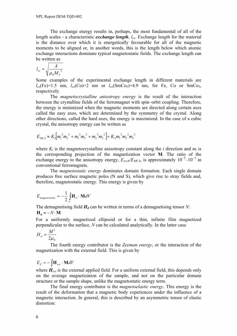
3. Measurement methods and metrological challenges. Current state and research outlook In terms of measurement techniques all magnetic properties can be divided into two categories: integral properties of the system (magnetization, magnetic anisotropy, transition temperature, etc.) and local properties of the sample (local distribution of magnetic moments, stray field, etc.). Corresponding physical methods and techniques used for measurements of magnetic properties also fall into two main groups, namely magnetometry and local probing of magnetic properties or magnetic microscopies. 3.1. Magnetization measurements There are two large groups of techniques for measurements of the DC magnetic moment based on either inductance or force detection. It should be noted that, generally, the quantity obtained in the experiment is the total magnetic moment. Magnetization of the sample can be derived by normalising the magnetic moment either by the mass or the volume of the magnetic material. Further refinement is obtained by considering the nanomagnet shape and correcting the experimentally observed values by the corresponding demagnetisation factor (see the discussion in Section 2.2). The inductive method based on moving a magnetized sample which causes a change of the magnetic flux in a pick-up coil, therefore, it induces an electromotive force proportional to the magnetic moment. Two main inductive techniques, namely vibrating sample magnetometer (VSM) [45] and Superconducting Quantum Interference Device (SQUID) magnetometry, have been well developed (Figure 2). In a VSM, the sample is vibrated in the vicinity of a set of pick-up coils. The flux change caused by the moving magnetic sample induces a voltage across the terminals of the pick-up coils that is proportional to the magnetization of the specimen and to the frequency of vibration f. The typical range of sample motion is about 1 mm with f in the range 10-103 Hz. The SQUID magnetometer operates basically on the same principal: the sample moves slowly through a pick-up coil set (1st or 2nd order gradiometer); the induced current flows through the signal coil of the SQUID and its magnitude is independent of f. Main operating parts of the SQUID magnetometer are the dewar, probe, superconducting magnet, SQUID assembly and electronic control system. Normally a SQUID magnetometer can be operated in DC, AC and reciprocating sample option (RSO) modes. Typical working parameters are i) a static field is up to 14 T with an accuracy of 10-5 T; ii) temperature is in the range 1.8-400 K with an accuracy of 0.01 K. The pick-up coils are configured as highly balanced second-derivative coils. The coils reject the applied field from the superconducting magnet to a resolution of 0.1%. The RSO mode gives the best sensitivity of the moment measurements down to 5×10-12 Am2 and, therefore, the most suitable for the research in nanomagnetism. In RSO mode a shaft encoder on the servo motor records the position of the sample synchronous with the SQUID signal. The data received is fitted to an ideal point dipole moment response. It limits the possible sample sizes (ideally sample size should be below 3 mm to match an ideal point dipole with an accuracy of approximately 0.1%). Additional options are a transverse moment detection system, horizontal and vertical sample rotation, sample space oven (up to 900 K), etc. Thus, high magnetic moment sensitivity, wide field and temperature
10
NPL Report DEM-TQD-002
operational range and flexibility of other working parameters make the SQUID magnetometer one of the essential instruments in the area of nanomagnetism.
a) b)
Figure 2. Schemes of inductive methods in magnetometry: a) VSM; b) SQUID.
Various physical phenomena forming a background of force magnetometry are based on the magnetomechanical effect discovered about 140 years ago. The force method relies on the fact that a magnetized sample placed in magnetic field gradient produces a resulting force on the sample which is proportional to its moment:
xBm
xEFBmE x ∂
∂=
∂∂
−=⇒⋅−=
Some of the first quantitative experiments in magnetism relied on measurements of torque due to fixed moments reacting to an applied field. Torque measurements require that the magnetic torque on a specimen reacts against mechanical deformations of a torque spring through magnetic anisotropies of the sample. Torque magnetometers are generally based on a torsional pendulum attached to a specimen suspended between the poles of a rotating dipole magnet [46]. Torque magnetometers are very sensitive and widely used to measure magnetic moments and anisotropies, with many improvements having been made over the last century. A different way to measure moment quantitatively is to immerse a specimen in a uniform field gradient, consequently generating a force. Two methods have been developed that work this way: the Faraday method [47] measures the force on a sample with a mechanical balance and the alternating field gradient magnetometer (AGM) [48] where an oscillating magnetic field gradient induces an alternating force on the specimen mounted on a flexible reed and, as a result, the specimen vibrates (Figure 3). A high sensitivity is obtained by choosing a vibration frequency equal to the mechanical resonance of the rod. Thus, the technique is the inverse to the VSM method since not an electromotive but a mechanical force is induced.
11

NPL Report DEM-TQD-002
a) b)
Figure 3. Schemes of force methods in magnetometry: a) Faraday balance; b) AGM.
Another group of methods is based on an angular-momentum absorption. Magnetic resonance spectroscopy is typically performed by placing a specimen in a microwave resonant cavity. When an applied background field is adjusted to match magnetic resonance conditions, the spins in the sample precess, causing a change in the Q of the microwave cavity due to enhanced power absorption on resonance. Magnetic resonance also generates internal mechanical torque. Torque induced by electron spin resonance (ESR) was first measured using a torque magnetometer [49,50,51] at frequencies ∼100-400 MHz. An extensive fundamental and industrial interest in magnetism on the nanoscale makes magnetization measurements more and more challenging as it requires a continuous increase of sensitivity and stability from all measurement techniques. Such giant industries as IT, automotive and biomedicine have been already actively working with nanomagnets. They require consideration and precise measurements of specific tasks related to novel ultra-high dense magnetic recording media, magnetic random access memory (MRAM), magnetoelectronics, interface magnetism, spin dynamics and switching as well as continuous sensor miniaturization. New ways are being developed to measure the magnetic properties of individual nanometre-scale particles. The ability to measure a single particle leads to a better understanding of quantum effects. Fundamental studies of surface and interface magnetism can also benefit from the development of more sensitive magnetometers. Magnetic moment sensitivities corresponding to a fraction of a monolayer film thickness or a single superparamagnetic particle (this corresponds to a cube of cobalt 8 nm on a side) are required to measure subtle changes in the magnetic moment. Instrumentation development is still on going, with a great deal of work being focused on combining magnetomechanical sensors with MEMS techniques. For example, notable applications of MEMS torque magnetometers include the de Haas–van Alphen effect [52], superconductor vortex dynamics [53], two-dimensional electron gas (2DEG) measurements [54,55,56], CMOS integrated gaussmeter sensors [57], and the measurement of thin-film moments and anisotropies [58]. In particular, these measurements led to the first observations of the deviation of the gyromagnetic constant from the value γe = −e/2me in ferromagnetic materials due to spin–orbit coupling [59]. One of the latest achievements in the area is a microresonating torque (force) magnetometer based on atomic force microscopy (AFM) principles developed at NIST [60].
12

NPL Report DEM-TQD-002
Figure 4. Measurements capability of magnetometry techniques.
Figure 4 reviews the current status of MEMS magnetometers relative to other techniques with some predictions for ultimate sensitivities. The term ‘conventional magnetometers’ refers to instruments designed for a large range of sample sizes and magnetic moments, i.e. torque, AGM and VSM (see Table I for details). For MEMS optimized magnetometers the sensitivity necessary to study specimens below the superparamagnetic limit at room temperature was predicted. The main challenge here is to develop fabrication methods for placing well-defined nanodots onto very sensitive cantilevers. Table I. Main parameters of ‘conventional’ magnetometers.
Method Sensitivity, Am2
Advantages Drawbacks
VSM
10-7
Easy to use, fast data collection.
Sample position is unstable due to shaking. Limited mass capability.
SQUID
down to 10-12
Highly sensitive, easy to use, suitable for the most materials.
Slow data collection, large range of movement, i.e. might cause problems with hysteretic samples.
Faraday balance
10-9
Fairly sensitive, reasonable data collection rate.
Applied field is ill-defined due to presence of large field gradient.
AGM
10-11
Sensitive, fast data collection.
Limited mass capability. Complicated ratio between the applied field gradient the coercivity.
Torque 10-11 Sensitive, suited for in-situ characterization.
Anisotropic samples (e.g. intrinsic, shape, films) are required.
As shown in Figure 4, there is a large range of relatively unexplored territory
below 10−12Am2 that is now accessible with the microsystems technologies being
13
NPL Report DEM-TQD-002
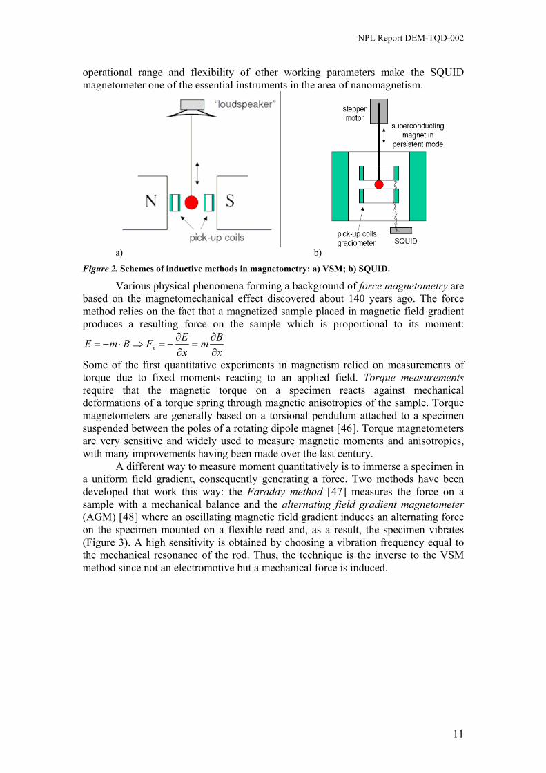
developed for magnetic measurements. The most sensitive technique, Magnetic Force Resonance Microscopy (MRFM), which allows a single spin resolution, is described below in Section 3.2. 3.2. Magnetic Microscopies A remarkable number of methods for direct, real-space imaging in magnetic microscopy have been demonstrated over the past decades. The continued development of high performance magnetic information technologies requires detailed study of the magnetostatics and dynamics of microscopic magnetic structures. Both fundamental curiosity (‘to see the world with our own eyes’) and industrial necessity now drive us toward innovations in magnetic microscopy for nanometer-length scale and femtosecond temporal resolutions, which are far beyond the limits of traditional imaging techniques. The magnetic microscopies currently in use may be vaguely classified into two (sometimes overlapping) groups, according to the physical mechanism of interaction between the probe and sample: i) stray field mapping and ii) magnetization mapping. 3.2.1. Stray field mapping For a long period of time, the iron filing method developed by Bitter offered the greatest spatial resolution. In the Bitter method, the surface of a magnetic material is dusted with magnetic nanoparticles. The particles agglomerate in the stray magnetic fields produced by domain walls. The final pattern is imaged under an optical or electron microscope, allowing very small, <100 nm, magnetic features to be resolved in multidomain ferromagnets, or in superconductors penetrated by a magnetic field. The instrument most widely used today is the magnetic force microscope (MFM) first demonstrated in 1987 [61,62]. In MFM, the magnetic contrast is achieved through the magnetostatic interaction between a ferromagnetic tip and the stray magnetic fields from the sample, in particular at domain boundaries (Figure 5). During measurements, a ferromagnetic tip is scanned at a certain constant height of several tens of nanometers above the surface. Thereby, the magnetostatic interaction between the stray field produced by the domain structure of the sample and the ferromagnetic tip is detected.
Figure 5. Scheme of the MFM technique.
MFM can be operated in the static and dynamic mode. Typically, lateral resolution is around 50 nm and the force gradient sensitivity is 10-2-10-3 N/m. Advantages of MFM include relatively high spatial resolution and simplicity in operation as well as sample preparation. A drawback is the difficulty of extracting
14

NPL Report DEM-TQD-002
quantitative information, although the interaction between the magnetic tip and sample is a very active topic of investigation. In particularly, quantitative magnetic force microscopy methods were developed to calibrate an MFM tip, calculate its stray field, and simulate magnetic force microscopy data [63]. One of the most important recent extensions of MFM is magnetic dissipation microscopy (MDM) [64]. The field from an MFM tip can perturb the magnetic structure of the sample. If this perturbation is cyclic and hysteretic, it leads to energy losses (as small as 10-14-10-13 watts) in the oscillating MFM cantilever which can then be quantified. In Magnetoresistance Sensitivity Mapping (MSM) the MFM probe can be used as a field source that excites the magneto-resistive sensor in a recording head. The resulting image shows the spatially dependent response of the sensor. This technique is a very useful for IT applications as it easily allows investigating the symmetry and sensitivity of giant magnetoresistance sensors (GMR). Magnetic resonance force microscopy (MRFM) is an adaptation of MFM based on the magnetic dipole interactions of a scanning cantilever tip and the sample. It is a force measurement method (and in this sense in a close correlation with techniques described in a previous paragraph) where the net magnetic moment of the specimen is modulated by bringing the spins in the sample in and out of resonance [65,66]. This gives rise to a modulated force on the cantilever, which is typically applied at the resonance frequency of the cantilever to improve signal-to-noise ratio. Recently a single spin detection at 1.6 K was performed by means of MFRM technique [67]. In this experiment (Figure 6) the magnetic tip at the end of an ultrasensitive silicon cantilever was positioned above a SiO2 sample containing a low density of unpaired electron spins. The resonant slice represents those points in the sample where the field from the magnetic tip matches the condition for magnetic resonance. As the cantilever vibrates, the resonant slice swings back and forth through the sample causing cyclic adiabatic inversion of the spin. The cyclic spin inversion causes a slight shift of the cantilever frequency owing to the magnetic force exerted by the spin on the tip. Spins as deep as 100 nm below the sample surface can be probed.
a) b) Figure 6. a) Configuration of the single-spin MRFM experiment; b) Spin as a function of sample position. The peak is believed to correspond to a single spin. Adapted by permission from Ref. 67: Macmillan Publishers Ltd: D. Rugar, et al. Nature 430, 329 (2004). Copyright 2004. Techniques using electron microscopes provide the highest presently available resolution. In Lorentz microscopy, for example, a high-energy (up 1000 keV) electron beam is incident on a thin (<150 nm) magnetic sample, and the magnetic contrast is derived from the deflection of the electrons due to the Lorentz force upon passing through the magnetization in the sample. Lateral resolution is better than 10 nm [68].
15

NPL Report DEM-TQD-002
Representative applications include the study of the detailed magnetic properties of nanoscale magnetic elements and patterned spin tunnel junction material [69]. The scanning of miniature field-sensing electronic devices such as Hall probes [70] or superconducting quantum interference devices [71] are further alternatives in the broad range of stray field mapping techniques. 3.2.2. Magnetization mapping The knowledge of the actual magnetization configuration within a sample is highly desirable in nanomagnetism. Numerous high-resolution magnetic imaging techniques measure quantities proportional to the local sample magnetization. These consist of interactions of i) electron, photon, or neutron beams with the sample or ii) atoms attached to sharp stylus-like probes. In magneto-optics, small rotations of the polarization plane of light upon reflection (Kerr effect) or transmission (Faraday effect) are used to map the magnetization. The first observation of magnetic domains by the Kerr effect was reported in 1951 [72]. Conventional magnetooptical recording is based on the same effects. The advantage of this method is in the possibility to apply an external magnetic field without influencing the probe, which is especially important for magnetization dynamics. The spatial resolution of the magneto-optic technique is diffraction limited, but the resolution can be significantly improved. For example, a resolution close to 100 nm was achieved using a high numerical aperture objective with a laser wavelength of 514 nm [73]. In x-ray magnetic circular dichroism (XMCD) microscopy, the contrast arises from the asymmetry in photon-absorption of atomic core levels that depend on the orientation of local magnetization relative to the optical helicity of incident circularly polarized soft x-rays. The most powerful feature of this technique is that magnetic domains can be imaged in an element-specific manner. Chemical specificity is obtained from tuning the excitation to the absorption edge of the desired element. This capability is useful for investigation of individual magnetic layers within multilayer structures [74] and for the study of alloys. X-ray microscopy also provides a powerful tool for imaging antiferromagnetism, by breaking the symmetry for core-level absorption of linearly polarized x-rays, whereas standard techniques are unable to spatially resolve magnetic domain structure in antiferromagnets. X-ray scattering is generally established for characterization of magnetic materials. Although early work concentrated on diffraction from bulk crystals, often of 4 or 5f series elements, reflectometry from 3d-element thin film samples was soon developed, and the first measurements of a coupled multilayer were reported by Tonnerre et al. [75]. More recently the technique has been widely applied, for instance to examine magnetic ripple in Co/Cu multilayers [76], spiral domain structures in L10 FePd films [77], exchange springs in Fe/Gd multilayers [78], antiferromagnetic coupling in Co/Ru multilayers [79] and reversal modes in patterned permalloy dots [80]. The ultimate resolution goal of most of the microscopic techniques described is to operate below the exchange length. Another objective is an ability to look directly at the interplay between magnetism and atomic structure with sub-nanometer resolution. In order to achieve this goal, the spin-polarized scanning tunneling microscope (SP-STM) was proposed and explored starting in the early 1990s [81,82,83,84] (Figure 7).
16

NPL Report DEM-TQD-002
Figure 7. The basic working principle of SP-STM is a spin-valve effect: since any ferromagnetic material exhibits a spin imbalance at the Fermi-level EF and the electron spin has to be preserved in an elastic tunneling process the conductivity of a tunnel junction must depend on the relative magnetization direction between tip and sample. (http://www.nanoscience.de/group_r/stm-spstm/).
By using a magnetic probe tip the SP-STM can be made sensitive to the spin of the tunnelling electrons. The basic working principle is well-known as spin-valve effect: since any ferromagnetic material exhibits a spin imbalance at the Fermi-level and the electron spin has to be preserved in an elastic tunnelling process, the conductivity of a tunnel junction must depend on the relative orientation of magnetization directions in the tip and sample. Tips may be magnetic (magnetically coated), or optically excited. SP-STM can measure both the in-plane as well as the out-of-plane magnetization component of the sample. The smallest magnetic features observed so-far were domain walls with a width of 0.6 nm in ferromagnetic iron films on W(110) and the atomic scale antiferromagnetic structure of a manganese monolayer. However, in practice, tip preparation and the separation of artefacts from the measurements have been great challenges.
Figure 8 and Table II summarize main characteristics of various magnetic microscopies.
Figure 8. Measurements capability of magnetic microscopies.
Magnetic microscopy has also addressed the extremely relevant for industries question of magnetization dynamics, including the ultrashort regime. High frequency
17

NPL Report DEM-TQD-002
(microwave) and fast time-domain phenomena are fundamental properties that are closely related to applications such as magnetic data storage and magnetic sensors. Considering the Gbit/s magnetic switching speeds of present technology, the temporal resolution necessary for characterizing dynamics in real devices is deep into the subnanosecond regime. An experimental tool for imaging fast magnetization dynamics has been demonstrated in time-resolved ferromagnetic resonance imaging experiments [85]. Recently, spatially detailed movies of magnetization reversal were reported [86], documenting the change in magnetization reversal mechanism caused by the presence of a transverse field. Time-resolved imaging with the second-harmonic MOKE [87] offers extreme sensitivity to the magnetization at surfaces and interfaces [88]. Table II. Main characteristics of magnetic microscopies.
Examples Spatial resolution
Advantages Drawbacks
Bitter method
<100 nm
Lorentz microscopy (Electron
holography)
10 nm (2 nm)
3D magnetic contrast; quantitative (differential phase contrast microscopy)
Complicated sample
preparation (tsubstrate<150 nm)
High energy beam
MFM (MDM, MSM)
>10 nm
Extracting of quantitative information (MDM)
Complicated real image representation
Stray field mapping
Electronic devices: SQUID
Hall probe
a few μm ≈250 nm
Magneto-Optics (Faradey and Kerr effects)
< wave length
SNOM <100 nm SEMPA ≈ 1 nm Magnetic sensitivity:
≈103 atoms
SP LEEM ≈ 10 nm
Magnetization mapping
SP-STM 1 atom (100 nm)
3D magnetic contrast; avoiding dipolar
interaction
Imaging spin dynamics
TR FMR Pump probe
magneto-optics
TR 2nd harmonic MOKE
TR XMCD New methods continue to appear and the last word in the magnetic microscopy techniques will probably never be told. One of the most exciting prospects in the field of magnetization dynamics is time-resolved XMCD, in particular, using the pulsed x-
18

NPL Report DEM-TQD-002
ray beam from synchrotron radiation sources [89,90]. A new generation of time-resolved XMCD will provide a lateral resolution of a few nanometers combined with a temporal resolution of 50 ps, along with chemical specificity. Another developing technique of great interest in this area is magnetic imaging using resonant scattering of coherent x-rays to allow domain reconstruction from experimental speckle patterns. Recently a novel method based on use of 1D Bose-Einstein condensate was demonstrated [91]. This technique combines relatively high spatial resolution (∼3 μm) and high field sensitivity (300 pT). Spatiotemporal imaging studies of combined electronic and spin transport have been successfully demonstrated in semiconductor systems [92] and are important to the development of spin electronics. The greatest promise that scanning probe methods hold is the possibility to build and study magnetic systems from the ground up, combining the techniques of atom manipulation with SP-STM and other pioneering probes of atomic-scale magnetism. Further developments and accomplishments to anticipate include exchange force microscopy [93], few- or single-spin detection and volume imaging by magnetic resonance force microscopy [94], single-shot and real-time ultrafast microscopy to capture stochastic and chaotic processes. 3.3. Equipment available at NPL Traditionally, magnetic measurements at NPL are mostly concerned with high-field high-moment applications. Equipment with sensitivity suitable for nano-magnetic studies is scarce. A Multimode AFM from Veeco is primarily used in the MFM mode at room temperature. A novel tuning-fork-based AFM for ultra-low temperatures is being developed and will have MFM capability. A UHV cryogenic STM has been used for SP-STM studies. This is a relatively unique piece of equipment, which is presently being enhanced to allow tip and sample conditioning vital for SP-STM experiments. Recently we have started a project (within the MET program) aiming the development of a new SPM based device capable of simultaneous measurements of elastic (piezo response, loss, friction and elasticity modulus), electrical (conductivity, spreading resistance, potential and surface capacity distributions) and magnetic (magnetic moment distribution) properties of multifunctional materials. A macro-scale magnetic field sensing/application system will be fabricated (based on commercial hard disk drive technology), to complement the SPM based systems. We plan a significant development of these machines by designing, manufacturing and testing of adjustable, insert cells. Such cells will create any required physical environment around the sample without disturbing the SPM head function. In particular, the cell will allow: i) to apply separately electrical and magnetic fields to the sample, where the fields might be oriented in three orthogonal directions; ii) to pass the electrical current between the scanning tip and sample. Moreover, a possibility to work in a variable temperature regime will be considered. The device will be suitable for work with bulk (in a few millimetres range) materials, thick/thin films and nanostructures.
However, for the rest we rely on a multitude of collaborations. Clearly, some serious investment in measurement infrastructure to support nano-magnetism is necessary, in particular, a sensitive SQUID magnetometer is the priority.
19
NPL Report DEM-TQD-002
4. Conventional ferromagnets on the nanoscale
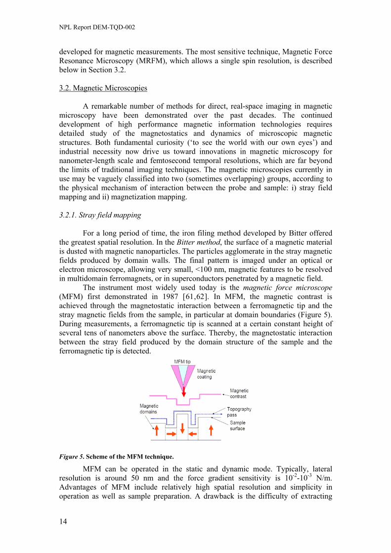
The main industrial driver is related to needs of information technology with its continuously increased storage density and processing speed. Near-future technical limitations will dramatically halt the current rate of increase in speed and capacity, hence, user demand will not be met. Industry widely uses scalable, non-volatile, magnetic memory systems based on continuous films that have doubled their storage capacity and speed every year and a half for the past 20 years, Figure 9.
a)
b)
Figure 9. Moore’s laws: a) device downsizing; b) chip density.
The “superparamagnetic limit” prevents further size reduction of the elements. This results from the requirement for the thermodynamic stability of the ferromagnetic element, which is critical in the use of magnetic bits for information storage. A magnetic bit will be stable if: KV > 55 kBT, where K is the magntocrystalline anisotropy constant of the material, V is the effective volume (i.e. grain volume in hard disc applications), k
B
BB is the Boltzman constant and T the temperature. For the best achieved value of the bit size (130×20 nm2, Barracuda 7200.8, Seagate) the ratio of the stored magnetic energy to the thermal energy is about
20

NPL Report DEM-TQD-002
200, which is already close to the superparamagnetic limit. Simply increasing K is not a long-term solution because greater static anisotropies require greater writing fields imposing other major technological barriers. As yet a patterned magnetic media where each dot represents a bit of information might provide the solution by overcoming the technical barriers inherent in existing technologies. The advantages of patterned magnetic media are:
• ultra high density up to Tbits/in2; • quantized writing process: lower noise and lower error rate; • nearly zero transition noise due to boundaries between bits being very
well-defined by preparation process; • reduced cross-talk between bits due to the absence of exchange
interaction and reduced magneto-static interaction; • flexible geometry of the array.
However, this approach can be relatively costly. Self-assembled magnetic media could provide an alternative solution (see the discussion in Section 4.2.1.). 4.1. Thin films and multilayers The majority of magnetic properties of (ultra-) thin films and multilayers originates on atomic and nanoscale [95,96,97,98] and differ significantly from the bulk properties of corresponding materials. The latter fact originates in a significant confinement of a z-dimension down to a few nanometres. Such confinement is a source of a numerous exciting physical phenomena which were not expected only 15-20 years ago, and it also allows consideration of thin films and multilayers as nanostructures. The revolutionary event starting the era of the novel magnetism took place in the late 1980s and related to discovery of GMR by a few groups around the world [17,18,19]. It was demonstrated that the resistance of alternating magnetic – non-magnetic layers changes enormously when placed in a magnetic field: the resistance becomes much lower if the magnetization in neighbouring layers is parallel and much higher if it is antiparallel (Figure 10). The effect originates in the difference in scattering of spin-up and spin-down electrons and ultimately leads to a dramatic increase of sensitivity in magnetoresistance measurements.
Figure 10. Schematic representations of spin-polarized transport from a ferromagnetic metal, through a normal metal, and into a second ferromagnetic metal for parallel and antiparallel magnetic moments.
21

NPL Report DEM-TQD-002
Following the discovery of GMR, the annual rate of increase in storage density tripled in following years. In 1997 IBM released a novel read-head device incorporating a spin-valve element which was based on GMR effect. Since its discovery, GMR remains the main example of the fastest route on the way from a fundamental invention towards a mass-production market. On the other hand, it stimulated a scientific community all over the world and turned it towards the nano-world. The rate of scientific publications on magnetism tripled in the late 1980s and still continues to grow. Besides the GMR effect, there are many other magnificent examples of novel physics which became possible only with reduction of the thickness to the nanolevel. Examples are moment modifications, i.e. its significant enlargement, at surfaces and interfaces [99,100], thickness-dependent domain-wall and coercive phenomena [101], interlayer exchange coupling [17,18,19] and finite-temperature magnetic ordering [102]. One of the most interesting phenomena from the fundamental point of view is oscillatory exchange coupling: the magnetic moments of two magnetic layers separated by a non-magnetic metallic spacer layer align themselves parallel or antiparallel, depending on the thickness of the intervening non-magnetic layer. It is one of the rare manifestations of directly observable quantum interference effects, which originates in confinement of electrons in a quantum well formed in the nonmagnetic layer by the spin-dependent potentials of the magnetic layers. A specific example of the nanoscale exchange-bias effects in multilayers [103,104] is of high industrial relevance, as it allows development of permanent magnet applications by exploiting the exchange-spring mechanism in nanostructured oriented magnets. The applications include engineering magnetic digital compensation points, increasing coercivity and fabricating magnetic exchange springs. 4.2. Nanostructured materials 4.2.1. Fabrication techniques Two approaches can be distinguished in a variety of methods for production of nanoparticles [105], namely ‘top-down’ and ‘bottom-up’ techniques. In the first approach one starts from a continuous magnetic thin film deposited on a non-magnetic substrate. The film is further patterned in order to remove all ‘excess’ of material and leave individual magnetic islands. Central to nanofabrication is lithography, a collective term for several closely related processes, including resist coating, exposure, and development. There is a large variety of lithographical methods, e.g. e-beam, x-ray, interference or holographic lithographies, etc. Lithography is usually followed by such preparation steps as additional masks deposition, chemical or dry etching, lift-off process and ion milling. The advantage of the ‘top-down’ approach is the possibility to preserve to some extent optimal magnetic properties typical for thin films, i.e. their epitaxiality, which leads to a predictable and controllable magneto-crystalline anisotropy of the nanomagnets. However, the production process is time consuming and costly, limiting the use of this method mainly by fundamental research. Lithography can also be used as a part of bottom-up approach for fabrication of nanometre sized templates on non-magnetic substrates. Such templates can then be filled with a magnetic material using a range of deposition methods or electroplating. In this method the template is usually removed (lift-off process) at the end of the
22

NPL Report DEM-TQD-002
production route, leaving free-standing magnetic structures. Novel lithography techniques allow fabrication of ordered magnetic nanostructures with desirable features, including arrays of elements with reproducible sizes in the range of 10 nm, which can be extended over large areas (up to S = 100 × 100 mm2). Using lithographic methods, magnetic nanostructures with a controllable shape can be prepared: from the simplest dots, bars and lines to advanced paths and array geometries. Besides lithographical techniques the bottom-up approach includes a wide spectrum of methods used for direct fabrication of ordered magnetic nanostructures. Examples are techniques based on scanning probe microscopes (STM and AFM) using voltage pulses [106], STM chemical vapour deposition [107,108] and STM local electrodeposition [109]. Despite the possibility of producing structures of only a few nanometers in size, the typical disadvantages of the other scanning probe techniques are a slow production process and small patterned area. Nanoimprint is one of the most industrially appropriate techniques in prospect. Whereas most conventional lithographic techniques are usually costly, complex and slow, the nanoimprint method has potential to overcome these disadvantages. Nanoimprint uses a mold to physically deform a resist, followed by ion etching [110,111]. Although an initial master mold has still to be manufactured by conventional electron lithography, the mold can be further reused or copied. Magnetic structures as small as 25 nm with periods of 150 nm have been fabricated using this technique [112]. Self-assembled nanostructures is a separate and very rapidly developing branch of the bottom-up approach which during the last couple of years has demonstrated the higher industrial impact than all other methods described above. There is a wide variety of natural processes which tend to form ordered arrays of nanostructures. However, although most of the resulting structures are ordered locally, they usually do not have true long-range order. The simplest example of self-assembly is heterogeneous nucleation when some magnetic atoms (Fe, Co) tend to nucleate at specific sites of the reconstructed surfaces, e.g. Au(111), Cu(111). For example, Fe tends to grow at the step edges of the Cu(111) surface or form ordered arrays of dislocations to relieve the stress, thus forming arrays of Fe lines or dots [113]. Several approaches for seeded growth have also been reported [114]. For instance, an array of non-magnetic nanostructures acts as a seed for the growth (usually by electroplating) of magnetic atoms, thus forming an array of magnetic particles. In a different approach, the magnetic particles are grown and coated in microemulsions (reverse micelles). These micelles are then deposited onto a substrate and under certain conditions they tend to form an ordered array on the substrate [115,116]. Growth in nanotemplates is the most developed method for producing self-assembled nanoparticles. There is a variety of techniques available to fabricate nanotemplates, including copolymer nanolithography [117,118], spheres lithography [119], alumina membranes and nuclear track etch method [120]. In particular, porous aluminum oxide membranes are among the most flexible, robust and cheap. The membranes have been fabricated by anodic oxidation of aluminium [121]. The oxidized film consists of packed columnar arrays of hexagonal cells, each with a cylindrical nanopore in the centre (Figure 11). By controlling the electrolyte species, temperature, anodising voltage and time, one can adjust the pore size, density, and height [121]. The resultant oxide layer has arrays of parallel cylindrical pores, perpendicular to the layer, separated from the unoxidized aluminium metal by a very thin layer of aluminium oxide. Typically, high-density pores (1–500 nm in diameter,
23

NPL Report DEM-TQD-002
109–1012 pores/cm2) can be achieved over a macroscopic area (>10 cm2) with small pore size variations. The pore separation is comparable to the pore size. These porous aluminium membranes have been used as growth matrices for arrays of Ni, Fe, Co [122], NiFe [123], CoNiCu/Cu [124] and Ge:Mn [125,126] nanowires as well as hollow Co nanotubes and Co/Ge nanocables [127].
Figure 11*. Top-down SEM image of as-synthesized AAO membrane with a pore diameter of 50 nm (Scale bar = 0.75 μm).
4.2.2. Magnetic properties The magnetic properties of the nanostructures are characterized by conventional techniques such as magnetization measurements (VSM, SQUID, AGM, MOKE, etc.), if the total magnetic moment of the array is larger than the resolution of the experimental system, or transport measurements, when the nanostructure presents a continuous conduction path (see Section 3.1). Also, certain local techniques (MFM, electron holography, micro-SQUID, etc.) have recently been developed to allow accurate characterization of a small number or even individual nanoelements (section 3.2). 4.2.2.1. Individual dots The magnetic properties of single dots depend on the balance of the exchange energy (favours homogeneous spin alignment, Figure 12a), the magnetic anisotropy (favours alignment of spins along a particular direction, Figure 12b), and the demagnetising field (favours minimal magnetization of the particles, Figure 13a). In ferromagnetic materials splitting into magnetic domains leads to a decrease of the stray field and therefore to reduction of the magnetostatic energy. The formation of domains depends on the balance of the exchange and magnetostatic energies, i.e. the gain in magnetostatic energy, due to the reduced demagnetising field, has to be larger than the energy cost of domain wall formation [128]. The formation of domains in magnetic nanoparticles has mainly two critical length scales: single domain size and domain wall width as was discussed in Section 2.2. The first one is directly related to the balance of energies in each nanoparticle and corresponds to the size at which the presence of a domain wall in the material is energetically favourable. It differs for different nanostructured magnets since the energy to create a domain wall is proportional to the square root of the anisotropy of the material but the magnetostatic energy is mainly related to the shape and the magnetic moment. The domain wall thickness λ, i.e. the width of the transition between the uniformly magnetized states of two domains (Figure 13b), is determined by the counterbalance between the exchange * Unless otherwise specified, all experimental figures are from our own research.
24

NPL Report DEM-TQD-002
energy (which tends to increase it) and the anisotropy energy (which tends to diminish it), see e.g. Ref. 128. It is evident that if the size of the nanostructure is of the order of the domain wall thickness, it can not be split into domains. Hence, nanostructures with sizes smaller than λ will remain single domain (Figure 12a). The term ‘single domain’ does not necessarily indicate a state where the nanostructures have uniform magnetization, but rather a state where no domain walls are present (Figure 13c).
a) b) c)
Figure 12. MFM images of a) single domain Co particles, size 150×450 nm; b) Fe circular nanomagnets, ∅ 500 nm, 4-fold symmetry reflects the high magnetocrystalline anisotropy of the sample; c) NiFe circular nanomagnets, ∅ 500 nm, with a vortex state which corresponds to a minimum stray field (typical for a material with low magnetocrystalline energy).
a) b) c)
Figure 13. MFM images of NiFe rectangular particles with lateral dimensions 300×900 nm and thickness: a) 50 nm – multidomain (double diamond state); b) 30 nm – Landau state (a domain wall with width of 40 nm is clearly observed) and c) 10 nm – quasi single domain or ‘flower’ state.
Both experimental observations and micromagnetic calculations have shown that there are many different possible variations of the stable single domain state depending on the nanomagnet shape, size or material, such as so called ‘flower’(Figure 13c), C- and S-states (with macroscopic net magnetization) or the vortex state (with zero net magnetization), Figure 12c. The numerous studies on the behaviour of individual dots have revealed that the main magnetic properties of these nanostructures are significantly different from those of continuous films: i) although the remanent state is essentially metastable, it is often possible to obtain a single-domain state at remanence; ii) shape anisotropy usually plays an important role in magnetization reversal processes; iii) coercive fields of the nanoelements are often larger than the values found in the unpatterned samples; iv) the spin wave spectrum is quantized due to the small size of the dots. An example showing a difference in the hysteresis curves obtained for a thin film Fe sample and for an array of circular dots prepared from the same film is demonstrated in Figure 14.
25

NPL Report DEM-TQD-002
a) b)
-0.8
0
0.8
-0.2 -0.1 0 0.1 0.2
M/M
s
B (T)-0.01 0 0.01
-2000
-1000
0
1000
2000
B (T)
Ms (k
A/m
)
Figure 14. Magnetization M(B) curves obtained for a) a continuous Fe(001) film, t=50 nm; b) an array of circular dots, ∅ 550 nm, prepared from the same film.
4.2.2.2. Arrays When the distance between the nanoelements becomes small enough, important interaction effects due to dipolar fields may be observed. Some of these dot interaction effects are: changes in coercivity and switching field distribution, presence of induced anisotropies, collective behaviours of the elements in magnetization reversal, or dynamic effects such as the shift of the spin wave frequency. The arrays of magnetic elements are also interesting due to their interaction with other systems. Arrays of magnetic dots can constitute effective ordered pinning centres for the vortex lattice when they interact with type II superconducting films (see Section 5.1.1). Also, ordered nanostructures can be used in hybrid semiconductor/ferromagnetic systems to produce a periodic magnetic field that modulates, in a controlled fashion, the transport properties of 2DEG materials. Effects of the dipole–dipole interaction depend strongly both on the distance between the centres of the dots and the gap between them. The change in the coercivity, one of the major effects of interaction, is more significant in systems with a small crystalline and shape anisotropy, i.e. with small saturation and coercive fields. Another important factor influencing the interaction between dots is their magnetization state. The direction of the moment, e.g. in-plane or out-of plane, also plays an important role due to the different kinds of dipolar fields. Another factor strongly affecting the interaction is the number and distribution of nearest neighbours. Hence, due to a complex combination of the above factors, reports on the interaction effects in arrays of nanomagnets are very contradictory: although some researchers claim negligible effects (see, e. g. [129,130]), others describe drastic changes (e.g. [131,132,133]). Contradictory results have been reported in different materials (e.g. Co, Ni, Ni80Fe20), or for differently shaped elements or arrays of the same material (e.g. Ni80Fe20). Coercivity enhancement, reduction or insensitivity to dot separation can be found in the literature. These discrepancies are the result of a number of factors, such as the type of array, magnetization state of the dots, switching mechanisms, and the fact that the nanodots are not simple dipoles. It has also been stressed that the field resulting from the dipolar interaction depends on the magnetization state of each dot, which in turn depends on the effective field of the neighboring elements. Consequently, the dipolar fields will change during the magnetization process.
26
NPL Report DEM-TQD-002
4.2.2.3. Dynamic effects The dynamic effects in magnetic nanostructures are becoming increasingly important at extremely small physical length and time scales (Figure 15). Issues such as magnetization reversal mechanisms, thermal stability, and ultrafast switching are both fundamentally interesting and practically important, for example, in ultrahigh density and high data rate magnetic recording and magnetic memory applications. Over recent years, advancements in magnetic characterization have enabled the study of individual nanomagnets (see, e.g. [134]). In typical magnetization reversal studies (not possessing a real time resolution) on individual magnetic entities, a magnetic field is applied opposite to the magnetization direction, and the reversal is characterized by MFM [27,135,170,], Lorentz-transmission electron microscopy [136], micro-SQUID [137], Kerr microscopy [138], or SEMPA [139]. However, from these types of measurements it is still difficult to understand the exact reversal mechanism. Even in the simplest case of single-domain particles, there are deviations from the Neel–Brown model of thermally assisted magnetization reversal over a single potential barrier [140,141]. Such deviations have been attributed to defects, geometry, and other imperfections in real samples, and have been shown to vanish in well-prepared single domain particles [137]. Under such collinear field magnetization configuration, the reversal speed is limited to the nanosecond level [137,140]. Alternatively, the reversal can be achieved by precession of the magnetization, induced by a pulsed reversal field applied perpendicular to the magnetization [142,143]. For micro- and nanomagnets, the reversal details are measured by Kerr microscopy [142,143], spin-dependent tunnelling and magnetotransport measurements [144,145], or time-resolved X-ray magnetic circular dichroism [146], which provide characterizations at the extremely short time scale. For arrays of nanomagnets, the collective behaviour is also important. The shift of the spin wave frequency observed by Brillouin light scattering is the most clear dynamic effect of interdot interactions [147,148], in agreement with theoretical predictions [149].
Figure 15. Comparison of dynamic excitations in continuous NiFe film and confined structures (circular dots, ∅ 550 nm) prepared from the same film. Results obtained using Brillouin light scattering technique operating in Damon – Eshbach mode.
Recently the possibility to detect phase-locked oscillations in neighbouring nanoelements was demonstrated by NIST [150] researchers. The spin torque effect
27

NPL Report DEM-TQD-002
that occurs in nanometre-scale magnetic multilayer devices can be used to generate steady-state microwave signals in response to a dc electrical current. The microwave power emitted from a single spin torque nano-oscillator (STNO) is typically <1 nW. To achieve a more useful power level (on the order of microwatts), a device could consist of an array of phase coherent STNOs. Electrical nano-contacts (∅=40 nm) to thin-film magnetic multilayer (CoFe/Cu/NiFe) mesas are dc current-controlled STNOs that produce microwave precession in the range 1-40 GHz, with spectral linewidths typically in the range 2–50 MHz at room temperature. The oscillations are detected by measuring the time-varying voltage across the device caused by the GMR effect and the dc current through the contact. Two STNOs in close proximity mutually synchronize (phase-lock). The phase-locked state is distinct, characterized by a sudden narrowing of signal linewidth and an increase in power due to the coherence of the individual oscillators. The phenomenon establishes a new functionality for magneto-electronic structures that are more commonly used as magnetic field sensors and magnetic memory elements. Arrays of phase-locked STNOs could be also used as nanometre-scale reference oscillators. Such devices could have applications in shrinking the size of microwave transmitters and receivers for wireless communications. A team from Freescale Semiconductor [151] reported similar results at the same time. They synchronized the phase of nano-oscillators 80 nm in diameter situated roughly 200 nm apart. The synchronized devices emitted frequencies of roughly 10–24 GHz. 4.2.2.4. 1D nanostructures Magnetic nanowires are scientifically interesting and have potential applications in many areas of advanced nanotechnology, including patterned magnetic media [152], magnetic devices and materials for optical and microwave applications [153] and as electroluminescent display devices [154]. Regular arrays of 1D magnetic structures are generally produced either by lithographical patterning or grown inside porous aluminium [121,122,125,126] (Figure 16). Other ways of fabricating cylindrical nanowires include the deposition into molecular sieves [155], track-etched polymer membranes [120,156] and mica templates [157]. Individual nanowires can be grown by a nanocluster-mediated vapour-liquid-solid growth method [158,159]. Large biomolecules are attractive templates for the nanowire synthesis. In particular, the tobacco mosaic virus is an ideal nano-template allowing production of Co and Ni nanowires with a diameter of 4 nm [160]. By electrodeposition into porous anodic aluminium [122] it is now possible to produce Fe, Co and Ni wires with diameters ranging from 4 to 200 nm, depending on the anodization conditions, and lengths of up to about 60 μm [125,126]. Typically, the nanowires form nearly hexagonal columnar arrays with variable centre-to-centre spacing of the order of 50 nm (Figure 11 and Figure 16a). Aside from the above-mentioned iron-series transition-metal elements, there is interest in depositing alloys and multilayers, such as Fe/Pt, into porous templates [161,162]. On the other hand, magnetoresistive effects have been investigated in electrodeposited Co–Ni–Cu/Cu multilayered nanowires [163] and resonant inversion of the tunnelling magnetoresistance in Ni/NiO/Co nanowires [164]. The 1D nanomagnets are characterized by important differences in their magnetic properties relative to unpatterned films: increase in coercivity, changes in domain structure and reversal mechanisms, quantization of spin wave modes, or dipolar interaction effects. Moreover, fabrication of tailored lines with modified shape has allowed the study of
28

NPL Report DEM-TQD-002
other topics, such as the contribution of the domain wall to the magnetoresistance, the speed of domain wall motion, or different giant magnetoresistance effects.
a) b) c) Figure 16. a) and b) plan and cross-section TEM images of mesoporous silica with 6 nm pores within the AAO channels; c) TEM image a cobalt nanotube within an AAO pore prepared using SCF deposition technique. Conventional microelectronics consists of a combination of memory and logic. Whereas numerous investigations are dealing with magnetic memories, the field of magnetic logic is much less explored. Such logic should operate with the basic Boolean functions, such as AND, NOT, and OR, as well as support signal fan-out and signal cross-over functions. Initial attempts have been made [165] to implement magnetic logic based on a single electron transistor architecture [166]. This scheme, magnetic cellular automata, used chains of magnetostatically coupled magnetic dots with nodal elements at the ends that have well-defined switching thresholds. Information propagated by magnetic solitons running across the chains, and logic functions were performed by summing stray magnetic fields. A different approach involves various MTJ-based magnetic logic schemes [167]. These designs have a number of advantages, including that the devices were based on existing MTJ technology and that the logic function could be programmed by changing the magnetization direction of the reference layer in the MTJ. However, high current densities were involved and high magnetoresistance ratios and large transistors were required. As an alternative architecture, a ‘domain-wall logic’ was developed (initially in Durham University), which uses no transistors and exhibits very little heating caused by data switching. In particular, a submicrometer planar nanowire made from a soft magnetic material such as permalloy has been shown to form an excellent medium for domain walls [168]. The high shape anisotropy of the nanowire ensures that magnetization prefers to align with the long axis of the wire. These two possible directions form the basis of the binary information, with a magnetic domain wall acting as the transition edge in a changing signal. Domain walls can be propagated through complex networks of nanowires under the action of an externally applied magnetic field. This field rotates in the plane of the device and acts as both the clock and the power supply. A complete logic architecture can be constructed, which uses planar submicrometer magnetic. Logical NOT, logical AND, signal fan-out, and signal cross-over elements, each of a simple geometric design, were demonstrated and can be integrated together into one circuit [169]. An additional element for data input allows information to be written to domain-wall logic circuits. Thus, it was demonstrated that spintronics promises an alternate route to traditional semiconductor electronics.
29

NPL Report DEM-TQD-002
4.2.2.5. Research outlook Finally, despite the active research in recent years, there is still a long way to fully understand the properties of magnetic nanostructures, even those composed from conventional ferromagnets. The fabrication of tailored nanostructures, particularly large arrays of ordered, ultrafine (<10 nm), homogeneously dispersed nanoelements, remains challenging. More systematic studies of the magnetization reversal processes are necessary, including the associated dynamic effects on short time scales. It is also crucial to achieve a good understanding of interaction effects in arrays of magnetic nanoelements, or between nanostructures of magnetic materials and other systems. The situation becomes even more complex when novel spin-engineered magnetic materials are used. The ever-developing industrial needs often require a combination of physical properties which does not exist in nature. Therefore, the fine tailoring of desired properties is a very important branch of the material science. In terms of spin-engineered materials, various magnetic hybrid structures (i.e. the structure where one component is a ferromagnetic thin film and another is, for example, semiconducting, superconducting or piezoelectric material) or non-magnetic host materials where a relatively small fraction of host atoms are substituted by transition or rare-earth elements (for example, diluted magnetic semiconductors and multiferroics) are in great demand. As a rule, these materials possess enhanced magnetic properties, such as higher magnetic moment, improved Curie temperature, etc. 4.3. Summary of NPL activity We have investigated magnetic properties of 0D (mainly in collaboration with Chalmers Univ., Sweden [170,171,172,173,174,175], but also with Seagate [176,177] and Sony [27,178]) and 1D (in collaboration with Cork Univ., Ireland [125,126,127,179]) nanostructures. Static and dynamic properties have been studied. Summarizing experimental results for 0D nanostructures, we can conclude:
• A stable single domain state in zero field was observed in nanodots made of all investigated conventional ferromagnets.
• Co-operation between the shape and magnetocrystalline anisotropies favours the single domain state.
• Magnetocrystalline anisotropy can be tuned by using multilayers of various chemical composition.
• Presence of interfaces influences significantly the zero-field domain structure and process of magnetization reversal. Switching properties of the nanomagnets depend on their shape and magnetocrystalline anisotropy.
• Dipolar interaction in the system leads to stabilisation of a single domain state.
These results are of importance for the development of patterned magnetic storage media and magneto-transport devices. Recently, we have started research on 1D ultra-narrow structures, e.g. cobalt and magnetite nanowires and nanocables with diameter down to 4 nm. These 1D nanostructures are among the narrowest ever studied.
30

NPL Report DEM-TQD-002
5. Novel (spin-engineered) magnetic materials
The main industrial drive is to create advanced materials which acquire specific magnetic properties non-existent in nature. In particular, the following material properties are of interest:
• enhanced magnetic moment and anisotropy; • coexistence of magnetic and semiconductor properties in a certain
temperature range; • multiferroic properties in a certain temperature range.
The main purpose of creation of all novel materials is to significantly improve their performance compared with materials existing in nature. Design and manufacture of spin-engineered materials is a huge area of Materials Physics and Chemistry, which has been developing very fast all over the world but mainly in the USA, Japan and Germany. Three main areas can be distinguished: i) hybrid structures, i.e. in the simplest approximation a multulayered thin (or ultrathin) film where at least one of the layers is a ferromagnet combined, for example, with either piezoelectric or semiconducting or superconducting layer. ii) 3D nonmagnetic host with embedded 1D nanomagnets. In the latter case the whole material possesses the magnetic properties. Some examples are multiferroic materials and diluted magnetic semiconductors. iii) Molecular magnets. 5.1. Magnetic hybrid structures 5.1.1. Ferromagnetic/superconducting structures Initially the co-existence of superconductivity and magnetism was deemed impossible. Indeed, on the macroscopic level, the well known Meissner-Ochsenfeld effect (1933) shows us that the external magnetic field is completely expelled from a superconductor. Recent research shows however that the two competing phenomena may co-exist in a variety of forms that give rise to a plethora of exciting effects. In this study, we shall only briefly mention some of these effects, such as exotic superconductivity mediated by the Cooper pairs with an angular momentum or chirality hence possessing a magnetic moment. We shall mainly concentrate on a number of recent experiments related to multilayered ferromagnetic/superconducting devices.
The BCS (Bardeen-Cooper-Schrieffer) theory explains superconductivity as due to an indirect (e.g., mediated by phonons) attractive interaction between an electron with momentum p and spin up (↑) and its time-reversed equivalent – an electron with the opposite momentum –p and spin down (↓), which couples the two in what is called a Cooper pair. The pair undergoes Bose-Einstein condensation at low temperature. In superconductors an applied magnetic field will eventually destroy the superconductivity primarily due to the orbital effect leading to violation of the time-reversal symmetry. The electrons of the opposite momentum get the common drift momentum q from the interaction, which provides them with different kinetic energies ξp→ ξp′= ξp+q, but ξ-p→ ξ-p+q≠ ξ-p′, thus lifting the degeneracy, which had been exact due to the time-reversal symmetry.
31

NPL Report DEM-TQD-002
5.1.1.1. Magnetic pinning of superconductng vortices
In the mixed state magnetic flux penetrates type-II superconductors as quantized vortices that interact repulsively, forming the so-called Abrikosov vortex lattice. Because the cores of the vortices are normal, the increased density of vortices driven by the applied magnetic field eventually displaces the superconducting phase.
When a current is sent through the superconductor the vortex lattice moves under the influence of the Lorentz force, thus causing dissipation. For practical applications it is therefore of crucial importance to firmly pin all vortices in order to achieve a high critical current density. Recent advances in electron-beam lithography have made it possible to create artificial pinning centres such as arrays of microholes (antidots) or ferromagnetic dots in a controlled and well-defined way. Of these two ways to manipulate the pinning strength, the one associated with magnetic nanoparticles is the most versatile.
The mechanism underlying the use of magnetic nanoparticles to pin vortices in a superconductor is that the stray field of the particle locally suppresses the superconductivity and a substantial energy is required for a vortex to escape from this potential well. The pinning array has to be carefully designed in order to optimise the current-carrying properties of the superconducting film. The size of the potential well dug in the superconductor by the stray field has to be of the same order as the vortex core (~ the coherence length of the superconductor, e.g., 38 nm in Nb). The array of dots has to be triangular to correspond to the symmetry of the Abrikosov lattice. As discussed above the period of the Abrikosov lattice depends on the magnetic field. Therefore, for a given spacing of the ferromagnetic dots, there exists a magnetic field at which the two lattices coincide. It was found that at this matching field the pinning strength is at maximum.
Figure 17. Mechanism of vortex pinning by stray field of a magnetic particle.
Hybrid structures consisting of superconducting films and ferromagnetic
pinning sites make it possible to change the pinning strength by switching between different magnetic domain states of the ferromagnetic nanosystems [180,181]. Furthermore, if the magnetic array is saturated in a high magnetic field, its pinning potential is significantly increased. This is because each individual nanodot reaches its single-domain state, and the stray field is significantly increased.
Ferromagnetic pinning centres do not necessarily have to be prepared in rather complicated lithographic processes. Also the domain structure in a continuous Co/Pt multilayer can strongly enhance the vortex pinning in a Pb film. Moreover, this domain structure can have a distinct influence on the nucleation of superconductivity in the Pb film ("domain wall superconductivity") [182].
32
NPL Report DEM-TQD-002
5.1.1.2. Pauli paramagnetic limit
If there were a way to prevent formation of the vortices, another pair-breaking mechanism limiting superconductivity will come into place. This mechanism is due to the effect of the external field on the electron spins. If the superconductor is in the clean limit (that is the mean free path of the electrons is longer than the superconducting coherence length; in other words – there are few impurities and scattering events are rare) and one can neglect spin-orbit scattering the ultimate limit for superconductivity would be when the magnetic energy, μBH, overcomes the binding energy of the Cooper pairs. When the magnetic field is large enough to magnetize the antiparallel paired electrons, the superconducting state would no longer exist. This limit was first described in a paper by Clogston [ , ] and often is called the Pauli paramagnetic limit. Soon after the Clogston paper, it was found that the upper critical field of a Pauli limited superconductor changes from a continuous to a first-order transition below t = T/T
B
183 184
c~ 0.5. After further study, it was proposed that if the magnetic field was able to interact with the electron spins and the superconductor were clean, the Cooper pairs could have non-zero momentum, and the order parameter would become spatially modulated [ , ]. This new type of superconducting state is commonly called the Larkin-Ovchinnikov-Fulde-Ferrel (LOFF) state after the theoreticians who predicted it. During the forty years since the introduction of this theory, physicists have looked for a superconductor in which the orbital motion is suppressed, so that the spin interaction or Pauli limiting dominates the high field physics.
185 186
Two properties of superconductors can suppress the orbital contribution. If the material is layered, that is, quasi-one- or two-dimensional (Q1D or Q2D), the carriers in certain orientations could not freely move from one layer to another, and the vortices could not form as easily. If the spaces between the conducting layers are large enough (larger than the superconducting coherence length, the nominal size of the vortices), the vortices could fit in the insulating layers of a Q2D superconductor and not affect the superconducting state. A similar idea works for a single layer too [187].* The search for Pauli limited superconductors has focused on two types of materials; the highly anisotropic organic superconductors and the heavy fermion superconductors. The cuprates, although highly anisotropic, have a large number of precipitates, and therefore are not good candidates.
In reality many superconductors can sustain fields in excess of the Pauli limit. This is because the treatment above is only valid for a clean superconductor or one with only non-magnetic impurities. Elastic scattering on non-magnetic impurities does not violate time-reversal symmetry of electrons in a Cooper pair and hence does not suppress superconductivity (Anderson, 1955). Magnetic impurities, in contrast, exchange momentum with the electrons of the Cooper pairs. The important difference to the case of a clean superconductor is that each inelastic scattering event gives an arbitrary contribution to the momentum in magnitude and sign and the overall effect has to be integrated over all possible paths. This randomising effect of spin-orbit scattering leads to a significant prefactor to the critical field, which may therefore exceed the Pauli limit.
The effects described above have many important consequences, such as the onset of gapless superconductivity, reentrant superconductivity, etc. The spatially
* Another way to subdue the orbital motion of the quasiparticles is to increase their effective mass, as in heavy fermion materials.
33

NPL Report DEM-TQD-002
modulated LOFF state unexpectedly found its analogue, when it became possible to produce Josephson junctions with a magnetic barrier. 5.1.1.3. Superconductor – ferromagnet – superconductor (SFS) Josephson junctions
For a long time, the observation of Josephson coupling in SFS junctions was a serious challenge. The solution to the problem of measuring supercurrents in SFS Josephson junctions was found by employing dilute ferromagnetic alloys in around year 2000. The first experimental observation of supercurrents in SFS junctions and the crossover from 0 to π state in Nb/CuxNi12x/Nb Josephson junctions was reported by Ryazanov et al. [188,189,190,191], and further phase-sensitive measurements by the same group [192].
Superconducting correlations induced in a ferromagnet differ qualitatively from those in superconductor – normal (SN) metal proximity systems. Generally, the proximity effect can be understood as a penetration of a Cooper pair amplitude into a nonsuperconducting material. An electron and a hole having opposite spins and momenta are correlated via Andreev reflection, thus providing an extension of superconductivity into a nonsuperconducting region. In the SN bilayer at a nonzero temperature these correlations decay exponentially with distance from the interface to the normal metal due to a dephasing between the wave functions of electrons and holes. In a superconductor – ferromagnet (SF) bilayer the correlated electrons and holes, having opposite spin directions, are under the exchange field of a ferromagnet. This results in an energy shift between these quasiparticles and the creation of a nonzero momentum q of Cooper pairs [193]. As a result, the amplitude of superconducting correlations oscillates spatially in the ferromagnetic metal as cos qx (see Figure 18). The sign change of this amplitude is equivalent to periodic 0-π phase jumps at certain points in the ferromagnet. Such an oscillating Cooper-pair amplitude is analogues to the LOFF state in magnetic superconductors discussed above. The oscillations in the ferromagnet decay with distance from the SF interface. There is a quantitative difference between the decay lengths of clean and diffusive ferromagnets. At T=0, the decay length in the dirty limit exactly coincides with the oscillation period [194,195]. In the clean limit the decay length is infinite at T=0 [196] and is limited only by elastic impurity scattering [197] or spin-orbit scattering [193] and typically exceeds the oscillation period. Therefore spatial oscillations are easier to observe in cleaner systems [198], but there is no qualitative difference between these two regimes.
Ic
Figure 18. Superconducting correlations in an SFS junction. Lines show the magnitude of the critical current Ic (maximum non-dissipative superconducting current that the Josephson junction can sustain) depending on the thickness of the ferromagnetic layer F. Sign change corresponds to the change in Ic direction with respect to the bias current (π shift of the CPR).
34

NPL Report DEM-TQD-002
The most remarkable property of S-F-S junctions is thus the possibility of realizing the π−state. Several groups have indeed observed this state [199,200]. For example, in Ref. 201 the current-phase relationship (CPR) was determined by incorporating the junction into a superconducting loop coupled to a dc SQUID, allowing measurement of the junction phase difference. Junctions fabricated with a thin (~ 22 nm) barrier of Cu0.47Ni0.53 sandwiched between Nb electrodes exhibited a re-entrant critical current with temperature, vanishing at T <Tπ ~ 2-4 K. It was found that the superconducting current is negative for T < Tπ, indicating that the junction is a π-Josephson junction.
The π-junctions provide new opportunities for the design of high-Tc sensors and circuits. As suggested by Terzioglu and Beasley [202], π-junctions are useful for the fabrication of complementary Josephson junction circuits, which are composed of standard SQUIDs and SQUIDs that contain a π-junction. These circuits are characterized by small power dissipation and large circuit margins. Because they result in a doubly-degenerate phase potential when incorporated into a superconducting loop, π junctions have been proposed as building blocks for superconducting qubits [203] - basic elements of a quantum computer.
In relation to the π junctions, of fundamental importance become the experimental techniques capable of measuring the CPR of a Josephson junction. An elegant rf technique to determine the CPR was first suggested some 40 years ago by Silver and Zimmerman and further developed to perfection by Il’ichev and co-authors [204]. In the rf method the Josephson junction of interest is inductively coupled to a tank circuit with known inductance, capacitance, and quality factor. The tank circuit is driven by a dc bias current and an rf current of a frequency close to the resonant frequency of the tank circuit. If the amplitude of the rf flux is small the CPR can be determined by monitoring the effective impedance of the tank circuit-interferometer combination as a function of the externally applied magnetic flux.
To summarize this section, the recent years brought us the understanding that superconductivity and magnetism are not always mutually exclusive phenomena, but can provide a useful combination of properties. In particular where it concerns nanoscale SF devices we would like to emphasize the complementary Josephson junction circuits, which can become the basis of ultrafast logic and memory devices of the future as well as elements (qubits) of quantum computers; and the artificial magnetic nanodot pinning centers, which become important in superconducting cables for high-power applications. Needless to say, these applications will be impossible without quantitative measurement methods for the magnetic fields and interactions on the nanoscale. 5.1.2. Ferromagnetic/piezoelectric devices One of the current goals in memory device development is to realize a high-density nonvolatile memory. Both magnetic random access memory (MRAM) [205] and ferroelectric random access memory (FRAM) [206] are promising candidates for non-volatile memory. The MRAM is generally composed of an array of patterned magnetic multilayer cells that exhibit giant or tunnel magnetoresistive properties [207,208]. A remanent state of a magnetic bit is based on a difference in magnetic resistance, which depends on a mutual orientation of spins in ferromagnetic (FM) layers separated by a nonmagnetic layer. The data bits are written in the cell by applying a local magnetic field excited by a pulsed current in an attached conductive
35
NPL Report DEM-TQD-002
strip. In order to achieve high-density memory in a MRAM device, the external magnetic field should be localized in a tiny cell to control the direction of spontaneous magnetization without any interference by neighbouring cells. As the magnetic cell size shrinks, it is more difficult to localize a magnetic field. In FRAM devices the basic concept for information storage is the same as in MRAM, but it uses switchable spontaneous polarization states which exist in ferroelectric materials such as PZT. Thus, to realize high-density storage MRAM devices it is crucial to develop a way to switch the direction of spin without applying a large external magnetic field*. Traditionally it could be done by heating, but this approach is essentially non-local and requires substantial power. Another possible way to control a magnetic state of the memory element is by using the magnetostriction effect, i.e. a change in dimensions of a ferromagnetic specimen under applying magnetic field, originating from the magnetoelastic coupling. Alternatively, the applied stress generates an internal magnetic field along which the magnetization prefers to align. Several ideas for the magnetic memory devices based on the magnetostriction behaviour have been proposed so far. One example is a MRAM device composed of an array of magnetostrictive transducers coupled with magnetic elements [209]. The magnetization reversal of the element is assisted by the stress wave generated by a selected transducer in a homogeneous applied field slightly smaller than the coercive field. Another application is a magneto-/electrostrictive hybrid thin film memory consisting of a magnetostrictive film in contact with an electrostrictive film [210]. For writing, the electrostrictive film is actuated to impart a stress to a selected area of the ferromagnetic film, which nucleates a poled domain in accordance with the applied field direction. Magnetostrictive 3D memory cells driven by ultrasonic pulses have also been proposed [211]. All of the above mentioned devices require both magnetic and electric fields for the writing process. Recently a possibility of stress-operated selective magnetization reversal in a small magnetic particle array with piezoelectric word lines has been proposed [212,213]. Calculations showed that only the magnetization of the particle positioned at the interconnection of active wires can be successfully switched (see Figure 19). The time delay and the pulse length are important in determining the dynamics of the magnetization reversal. The speed of the reversal is limited by the ferromagnetic resonance frequency of order a few GHz. The nondestructive reading process can be achieved by incorporating the magnetoresistive junctions into the magnetostrictive/piezoelectric memory cell.
This proves the possibility of a stress operated memory device in which the magnetic state is fully controlled by the magnetostrictive effect. On the other hand, Lee et al. [214] have recently demonstrated that the spontaneous direction of magnetization in FM films could be controlled by the inverse piezoelectric effect in PZT films with low driving voltage. They showed a clear spin-reorientation transition in CoPd alloy films on the PZT substrate, where the electric field is applied normal to the film plane. The electric field dependence of polar Kerr rotation was shown to be strongly dependent on the composition of the CoPd alloys. A further approach was suggested by Borisov et al. [215] using magnetoelectric hybrid structure Cr2O3(111)/(Co/Pt)3. Chromium oxide is the archetypical magnetoelectric material which retains these properties above room temperature. This makes it interesting for devices involving the exchange bias (EB)
* Current-induced switching, when a spin-polarized current applies a large enough torque to switch the magnetization without the need for an external field, can be an alternative approach.
36

NPL Report DEM-TQD-002
effect appearing at the interface between exchange coupled ferromagnetic and antiferromagnetic (AF) thin films.
Figure 19. Time evolution of magnetic states for particles positioned on single word lines (A and C) and a cross-section of word lines (particle B). The magnetization of the particle B is switched, whereas the final magnetic states of the particles A and C are not affected. Reused with permission from Ref. 212: V. Novosad, et al. J. Appl. Phys. 87, 6400 (2000). Copyright 2000, American Institute of Physics. EB systems are of great practical importance as they are widely used in MRAM cells and GMR read-heads. A possibility to control interface magnetization by application of an external electric field has been proposed [216]. A novel switching mechanism for the EB field is based on the magnetoelectric field cooling process, which favours the growth of a distinct AF single domain and thus an efficient control of the AF interface moment. The possibility to control the interface magnetization using the piezomagnetic effect was also observed, e.g., in Fe0.6Zn0.4F2/Fe [217]. On the other hand, a reversible external electric field induced modulation of room temperature magnetic moment as well as a coercive field in an oxide-based diluted magnetic semiconductor has been recently demonstrated [218]. A strong modulation, ~15% for the magnetization and ~40% for coercive force, was realized in an epitaxial heterostructure of PbZr0.2Ti0.8O3/Co:TiO2/SrRuO3 grown on (001) LaAlO3. Observation of electric field effect strongly favours the intrinsic (i.e., carrier-induced) nature of ferromagnetism in the high temperature grown insulating Co:TiO2 films. The last experiment demonstrates the possibility and necessity of a synergetic and multifunctional (piezoelectric and diluted magnetic insulator materials) approach both for tailoring of novel magnetic materials and deep understanding of their fundamental magnetic properties. 5.1.3. Ferromagnetic/semiconductor devices. Spin injection Progress in increasing the speed and processing power of silicon chips continues to follow the well-known ‘Moore’s law’, postulating that computing power doubles roughly every 18 months (see also the discussion in the beginning of Section 4). However, these devices operate on the same basic principle of controlling the flow of current by an applied voltage that was used in the first transistor more than 50 years ago. It has been recently theoretically predicted that for a gate size approximately 22 nm the conventional (charged-based) silicon transistors will lose their functionality. Thus, in order to maintain the high development rate, the world below 22 nm should be operated by different physical phenomena. In particular, to solve this problem Intel has proposed in its road-mapping (covering the period up to 2020) so-called
37

NPL Report DEM-TQD-002
revolutionary (e.g. nanowire or group III-V based) or exotic (e.g. organic molecules based) CMOS (Figure 20).
Figure 20. Road-mapping of transistor development by Intel.
As an alternative to conventional silicon logic, a non-charged based logic was suggested, where devices exploring an electron spin in addition to charge were recommended. This emerging field of spin-based electronics may lead to new classes of semiconducting microprocessors and memory chips with greatly increased functionality [219]. The discovery of such effects as GMR in metallic multilayer structures has already led to much more sensitive position sensors (used in automobile braking systems), perimeter defence systems, magnetometers, non-volatile memory chips and read heads used in computer hard drives and disk storage systems. The ability to produce ferromagnetism in semiconductors above room temperature would lead to devices such as light-emitting and laser diodes with polarized output, transistors with ultra-low power use, magnetic devices with gain, integrated logic and memory chips (leading to computers that would turn on immediately like a television set, without having to boot-up the operating system that is currently stored in magnetic memory on the hard drive), and powerful remote sensor systems that incorporate magnetic detection functions with on-chip signal processing and off-chip optical communication. Semiconductor lasers fed by spin polarized currents will have better mode stability and lower critical currents. Similarly, a spin transistor consisting of a semiconductor sandwiched between ferromagnetic contacts is expected to be faster and more efficient than a standard field-effect transistor.
Magnetoelectronic effects are based on the spin polarization of electrons, holes and currents or both in semiconductor devices. The major ingredients for its realization are i) the transfer of spin information into a semiconductor device (spin injection), ii) the manipulation and storage of the spin and iii) the detection of the spin information. Various experiments have addressed one or more of these three topics and have shown the feasibility of magnetoelectronic devices. The most straightforward approach is the one employed in MRAM, where an array of magnetic memory elements is placed on top of a semiconductor wafer containing transistors and other circuitry required to drive the memory (Figure 21a). This requires a modest, yet not trivial integration at the system level, but does not take advantage of the unique properties of semiconductors in manipulating spin. A different approach is to create hybrid device structures in which ferromagnets and semiconductors are combined.
One could think of many different geometries for such hybrid structures. Two main categories will be distinguished, based on whether the control and manipulation
38

NPL Report DEM-TQD-002
of the spins occurs in the semiconductor or in the ferromagnetic material. This approach has established much better progress, where a device concept has been successfully demonstrated by Monsma et al. (Figure 21b) [220] with the introduction of the spin-valve transistor in 1995, and the subsequent observation of huge magnetic response at room temperature a few years later (for the latest review see Ref. 221).
a) b)
Magnetic memory array
Si wafer with circuirty
Figure 21. a) Hybrid system comprising semiconductor/ferromagnetic elements. b) Schematic cross section of Monsma transistor and energy band diagram of the spin valve transistor under forward-bias emitter Schottky barrier and the reverse-biased collector Schottky barrier as well as ballistic and scattered electron transport. Figure 21 b is reprinted with permission from Ref. 220: D. J. Monsma, et al., Science 281, 407 (1998). Copyright 1998 AAAS. The main trigger for the search for spin injection was the discovery of GMR effect in the late 1980s. The simplest idea was the substitution of a non-magnetic layer in a basic GMR stack by a semiconductor material. Implementing spin-polarized current transport in a semiconductor enables a new concept in spin transistor design - the spin-polarized-injection current emitter (SPICE) device. In SPICE the emitter injects a spin-polarized current and a spin-selective guard-rail determines if these polarized carriers have reached the collector or not. Electrical characteristics of such device may easily be switched by manipulating the externally applied magnetic field. A wide variety of designs are possible where the emitter and collector interfaces may be realized by p–n junctions, Schottky barriers or spin-tunnel junctions depending on the device application. Direct experiments on spin-injection into semiconductor were performed [222]. Interestingly, the observed spin-diffusion length was very large, in the order of a hundred micron and the effect decays only very slightly with silicon channel length. Moreover, experiments suggest that spin-tunnel injection into semiconductors is a promising technique which offers higher injection efficiency than direct spin injection [223]. Further results in this area are imminent. However, the spin transport effects are just of the order of a few per cent at best. Thus, the spin-injection process at the metal/semiconductor interface is highly inefficient. The source of this effect is in the differences in spin diffusion between semiconductors and metals originating from: i) the much greater spin relaxation lifetime in semiconductors, ii) insufficient screening in semiconductors relative to metals. Therefore, although it has been experimentally established beyond reasonable doubt that spin diffusion lengths in semiconductors are more than adequate [224] to enable construction of semiconductor spin-electronic devices, high yield direct spin injection from FM metals into semiconductors has so far eluded experimenters. To
39

NPL Report DEM-TQD-002
date, attention has mainly focused on injection into 2-D semiconductors [225,226,227] since this is the ideal system for realization of the Datta-Das transistor [228]. The authors proposed a device in which a spin polarized electron current through a semiconductor 2DEG is modulated by an electrostatic gate via the spin–orbit coupling. The Datta-Das transistor represents a GMR like device in which the non-magnetic metal layer is replaced by a semiconductor mesa. The authors proposed to use, e.g. Fe as a ferromagnetic spin injector and detector. Many attempts have been made to realize this device [229,230,231]. Most of these experiments were based on low band gap semiconductors like InAs or (In,Ga)As, which allow for the fabrication of low resistance ohmic contacts, and typically used contacts are made of Fe, Co or permalloy. However, the results for these direct experiments were far away from industrially acceptable. Theoretically it was explained [232,233] why direct injection into two-dimensional semiconductors is so disappointing. The fundamental problem is a continuity of the electrochemical potentials at the interface in the absence of interface scattering (Figure 22). Finally it results in the difference in conductance of the contacts that are used and the semiconductor into which the spin polarized electrons have to be injected. It was shown [232] , that the spin transport through a semiconductor can mostly be described by the electrical boundary conditions at its interfaces to the contacts, provided that the transport is diffusive and the spin scattering is low. This means that the spin-accumulation density is very small in the semiconductor: hence also is the spin-polarized current through the interface which feeds it.
Figure 22. Semiconductor-ferromagnet interface. Reprinted with permission from Ref. 234. Copyright 2002, IoP Publishing Limited.
It was shown [233] that the great enemy of ohmic spin injection is loss of polarization in the FM/semiconductor heterostructure, either by spin flipping at the interface or within a spin diffusion length at the interface. The key to success is then to suppress this spin flip channel. The origin of interface spin flip is a difficult subject, as yet not fully understood. For direct ohmic contact between FM (high density of
40

NPL Report DEM-TQD-002
states (DOS)) and semiconductor (small DOS) spin flip loss in the FM dominates and spin-injection efficiency is poor. The exception is the half-metallic ferromagnet where FM spin-flip loss is suppressed by the complete absence of final states for spin flipping. However, several recipes have been suggested for spin-flip control in conventional ferromagnets which do not involve direct ohmic contact. The new approach is to insert a thin layer of some material between FM and semiconductor which defines the injected polarization independently of what is happening in the bulk FM and delivers that polarization intact to the semiconductor. Usually this intermediate layer is a tunnel barrier of some variety. Three particular cases of the intermediate layer configuration can be considered: a non-magnetic tunnelling barrier, a magnetic tunnelling barrier and a Schottky barrier. Non-magnetic tunnel barrier. The simplest intermediate layer injector is a FM/non-magnetic tunnel barrier/semiconductor sandwich. Insertion of the intermediate layer changes completely the electrochemical potential diagram (the huge gap in the electrochemical potential at the interface). The key to the successful operation of the new arrangement is that the voltage dropped on the tunnel barrier is very large compared with the electrochemical potential deviations and hence totally controls the injected current and its polarization. Thus, introducing a non-magnetic tunnel barrier between FM and semiconductor makes a dramatic improvement (several orders of magnitude) to spin-injection efficiency. In particular, Van Dorpe et al. have demonstrated an increase of the spin polarization degree up to 24% at 80 K, persisting to 12% at room temperature in NiFe/CoFe/GaAs heterostructures through a conventional aluminium oxide barrier [11,235]. Magnetic tunnel barrier. An alternative is to use a spin-split magnetic insulator as tunnelling barrier. In this case the spin polarization can approach 100%. The insulator band splitting means that the two spin channels see different tunnel barrier heights and their evanescent decay rates are different depending on the particle spin. The transport properties of spin split europium-based insulators have been studied [236,237] at low temperatures and the results suggest that the device might act as convincing spin polarizers. Since no metal is involved, no problems of Schottky barrier interface states and differential material resistivities arise and the insulator/semiconductor combination affords a high degree of flexibility in choosing the point on the semiconductor band structure where spin injection occurs. However to date, little practical use has been made of these materials. The Schottky barrier injector. Another method of defining an intermediate layer between FM and semiconductor is to implement a Schottky barrier whose depletion zone is the intermediate layer. In principal, in a majority of cases Fermi electrons can not enter the conduction band of most semiconductors from a metallic contact without undergoing a tunnelling process, i.e. tunnelling through a native Schottky barrier. By inserting a thin, heavily doped semiconductor layer at the interface with the metal, a good tunnel contact can be achieved. By heavily doping of part of the semiconductor layer, the effective Schottky barrier thickness is reduced. For example, in order to observe notable spin polarization of the electrons (up to 6%) the light emitting diode (LED) structure consisting of five additional layers of n-AlGaAs was used [238] where the donor concentration was increasing from 5x10¹⁶ to 1.5x1019 cm-3 towards the MnSb ferromagnetic electrode. Evidently, as temperature rises, the thermal process becomes more competitive and spin-injection performance worsens.
41

NPL Report DEM-TQD-002
5.1.4. NPL research on magnetic hybrid structures
NPL activity in superconductor-ferromagnet structures is marginal at present. However, given our track-record in development of superconducting devices and present interest in various implementations of quantum bits, we are naturally interested in S-F-S devices, which may offer an interesting alternative to conventional Josephson junctions. This work should enable NPL to be well positioned to provide understanding and metrology on qubit structures as the QIP industry sector emerged. S-F structures with enhanced vortex pinning on the other hand may attract immediate interest from the industry involved in production of superconducting wire for high-current applications, such as Oxford Instruments. Here we could potentially offer expertise in material characterization from both the magnetic and the superconducting prospectives. Recently we have demonstrated the possibility of realization of artificial spin-chains in circular sub-micron dots consisting of hybrid ferromagnetic/tunnelling barrier structures (pillars consisting of alternating discs of permalloy and Al2O3) [175], see Figure 23. Spin chains are the most basic elements in the description of magnetic ordering phenomena although hardly ever studied in nanomagnets. We showed that dipolar coupling between the magnetic discs results in an antiferromagntic ground state, which was confirmed by model calculations and experimental magnetization loops.
Figure 23. Schematic picture of the pillar structures. The bright discs represent Al2O3 (1.8 nm thick), the dark discs permalloy (3.0 nm thick). The total structure consists of 10 permalloy/Al2O3 repeats, resulting in a total height of ~50 nm.
We plan to develop further the research in the area of hybrid magnetic structures. In particular, NPL is a participant in the proposal (PiezoMag) which was recently submitted to FP 6. The strategic objective of the project is the manipulation of the magnetic anisotropy, using magnetoelastic properties of magnetic alloys through an interaction with piezoelectric materials. We plan to study hybrid nanosystems consisting of ferromagnetic and piezoceramic materials (Figure 24). This is a completely novel approach to overcome near-future limitations for the application of magnetic systems in future emerging information technologies combining the best properties of multifunctional (piezoelectric/ferromagnetic) materials. New structures with high technological impact will be created for applications such as: recording media, multifunctional sensors and high-speed signal processing.
42

NPL Report DEM-TQD-002
Figure 24. A proposed scheme of the hybrid piezoelectric/ferromagnetic nanodevice with an array of individually addressed elements.
5.2. Diluted magnetic semiconductors (DMS) 5.2.1. Theory and experiment The rapidly developing field of spin electronics represents the concept of the synergetic and multifunctional use of charge and spin dynamics of electrons, aiming to go beyond the traditional dichotomy of semiconductor electronics and magnetic storage technology [239]. Such new functionalities require new materials encompassing both semiconducting and magnetic properties. The most direct method to induce spin-polarized electrons into a semiconductor is by introducing appropriate transition metal or rare earths dopants (such as Fe, Ni, Mn) at level of a few percents, producing a dilute magnetic semiconductor (DMS) [240,241], Figure 25. Thus, DMS (even in their bulk state) can be naturally characterized as nanomagnets, as they represent a non-magnetic matrix with individual magnetic atoms embedded. DMS materials exhibit desirable properties from both sides and offer unprecedented opportunities for spintronics devices. Usually, magnetic moments originate from the unfilled 3d or 4f shells of correspondent dopants. Generally DMS materials have been reported in III-V, II-VI and IV groups of semiconductors [242,243,244] and in oxide hosts [245,246,247]. Unfortunately, possibilities of artefacts such as dopant clustering, impurity magnetic phases, etc. have been noted in some cases under certain growth conditions [245,247,248,249].
Figure 25. Schematic representation of a DMS material.
DMS materials exhibit a spin-dependent coupling between localized states and those in the valence and conduction bands. The carriers (usually holes) in DMS mediate a ferromagnetic interaction between the localized spins. This means that it is possible to control magnetization by an electric field, which affects the carrier density in semiconductors. This has been achieved in Mn-based III-V semiconductors, e.g. (In,Mn)As and (Ga,Mn)As, and in Mn-doped II-VI semiconductors, e.g. (Cd,Mn)Te/(Cd,Mg,Zn)Te:N. In the case of (Ga,Mn)As, the most extensively studied DMS material, the Mn atoms introduce both the spins and the holes that mediate the coupling between the localized spins, and give rise to ferromagnetism. On the other hand, in (Cd,Mn)Te/(Cd,Mg,Zn)Te:N the holes must be brought in by additional nitrogen doping.
43
NPL Report DEM-TQD-002
The qualitative theoretical picture of DMS ferromagnetism in Ga1–xMnxAs has been developed by insights from several different approaches. Extensive ab initio electronic structure studies can account for important materials trends and qualitative features of the exchange interactions between Mn ions and band electrons [250,251,252,253,254,255,256]. For example, it was demonstrated that Mn acceptor levels are more localized in nitrides than in arsenides or phosphates. Ab initio electronic structure calculations have helped to understand materials trends within both II–VI- and III–V-based Mn DMS families and have provided useful guidance for other promising families. However, the prediction of exchange interaction strengths and ferromagnetic transition temperatures in an individual material is sensitive to approximations made in treating electronic correlations. It is now generally agreed that the local density approximation (LDA) does not produce accurate values for the strength of the interaction between Mn and valence-band spins. For (GaMn)As, it results in an overestimate of exchange interaction strengths. This deficiency might be eliminated by the use of LDA+U method which takes into account orbital dependence of the Coulomb and exchange interactions which is absent in the ‘pure’ LDA [256,257,258].
A complementary phenomenological approach [259,260,261], which introduces a single free constant Jpd to characterize the strength of the exchange interaction between Mn and hole spins, cannot address material trends, but has succeeded in explaining many details of the properties of (GaMn)As and similar materials. The resulting model, in which ferromagnetism arises from exchange coupling between local moments and band electrons, is often referred to as the Zener model [262]. As applied to (GaMn)As and related materials, the Zener model assumes that valence-band hole states in the DMS are formed from states near the valence-band edge of the host semiconductor. The applicability of this model to any given material, and the value of the phenomenological parameter Jpd, must be established either by comparison with experiment or on the basis of reliable ab initio calculations. For example, this model was used in Ref. to predict properties of materials like (Zn,Mn)O and (Ga,Mn)N, but later experiments have shown that it is not appropriate for these systems. Although the Zener model is simplified, its properties are still complex because of the combined influence of interactions and disorder. It is most easily analyzed when the dilute Mn ions are modeled as a magnetic continuum and spatial fluctuations in the magnetization orientation are not taken into account, i.e. mean-field approximation. This approach suggests a strategy that can be used in the search for high-TC materials: i) systems with strong exchange interactions and ii) a large valence band density of states. However, this tactic works only up to a certain point, because strong exchange coupling leads to more localized acceptor levels that will not effectively couple Mn ions located at different lattice sites. Similarly, a large valence-band density of states implies a large effective mass and this also leads to more localized acceptor levels. Mean-field theory has been very successful [257] in explaining many magnetic and transport properties of (GaMn)As. In mean-field theory, the transition temperature increases without limit with both the exchange interaction strength and the hole density. But these trends cannot continue indefinitely because strong exchange interactions will eventually localize holes and high densities will lead to interactions that vary rapidly in space. Thus, presumably, no single model is capable of explaining the properties of the wide class of dilute magnetic semiconductors, and various possible explanations have to be taken into consideration at this stage.
44

NPL Report DEM-TQD-002
The ability to tune the ferromagnetism of (Ga,Mn)As by varying the Mn content ratio and by an electric field can already be exploited in quantum information hardware, such as spin sources and detectors of single spins. However, the impact of these semiconductors for spintronics applications is restricted by a relatively low Curie temperature (TC) — the temperature above which a ferromagnetic material loses its permanent magnetism. Despite steady progress, TC remains at only 170 K in Mn-doped GaAs. Thus, the development of new ferromagnetic semiconductors with appreciable spontaneous magnetization and coupling between semiconductor and magnetic degrees of freedom at room temperature has become a vital challenge of materials science. Extensive research has been carried out in order to create DMS materials with well-established room temperature ferromagnetism. Despite several encouraging results [263], DMS materials are still struggling to reliably achieve the desired high Curie temperature, Tc. The Mn-doped wide-band gap nitrides, e.g. (Ga,Mn)N, and oxides, e.g. p-(Zn,Mn)O, are particularly promising in this regard. The short bond lengths in these materials leads to a strong coupling between the holes (which reside on the anions) and the spins (localized on the magnetic cations). For example, Tc above room temperature was first theoretically predicted in (Ga,Mn)N by the hole-mediated exchange interaction model [264] and later observed experimentally in thin film samples [265]. In particular, the existence of room temperature ferromagnetism in Mn-doped GaN nanowires was recently reported [266,267]. A spontaneous magnetic moment at room temperature was also observed in a wide class of magnetically doped nitrides and oxides, such as (Al,Cr)N [268], (Zn,V)O [269], (Zn,Co)V [270], and (Sn,Co)O2 [271]. Nearly all materials with high Tc belong to wide-gap semiconductors, see Figure 26.
Figure 26. Predicted Curie temperatures as a function of bandgap, along with some experimental results. Reprinted with permission from Ref. 272. Copyright 2004, IoP Publishing Limited.
Conversely, room temperature ferromagnetism in narrow-band gap group IV
semiconductors is not expected. In particular, a Tc=80 K for Ge0.95Mn0.05 was anticipated by Dietl et al. [264]. Recently effective pair exchange interactions in GeMn have been studied ab initio as a function of the distance between magnetic atoms as well as concentrations of the Mn atoms and compensating defects [273]. The authors [273] showed that the value of Tc depended on the Mn concentration, being up to 175 K at a Mn concentration of 3.5%. Experimentally it has also been demonstrated that in epitaxial Ge1-xMnx films Tc increases linearly with Mn concentration from 25 K to 116 K [243]. It was shown that the careful choice of growth parameters, i.e. type of substrate, growth temperature and concentration of magnetic impurity, is crucial for achieving the optimal magnetic performance [274,275]. Although works cited
45

NPL Report DEM-TQD-002
above are rather controversial, formation of secondary-phase ferromagnetic alloys in these references was excluded and all observed effects were attributed to a pure DMS type of ferromagnetism. At the same time, a more conventional type of ferromagnetic ordering is frequently observed in Ge:Mn compounds (see, e.g. Ref. 276) due to formation of various second-phase GeMn nanoclusters (10-100 nm size) in a semiconductor host or DMS matrix. Recently it has been shown that co-doping of GeMn by an additional transition metal, i.e. cobalt or iron, causes a significant increase both in the magnetic moment and Tc [277,278] up to Tc=350 K. Thus, whereas the DMS type of ferromagnetism in GeMn was usually observed at low temperatures, ferromagnetism caused by formation of Ge-Mn and Ge-Mn-Me alloys is characterized by a higher (up to and above 300 K) Curie temperature.
Special attention has been given to group-IV semiconductors due to their compatibility with existing silicon technologies. In particularly, germanium is closely lattice matched to the AlGaAs family and has a higher intrinsic hole mobility than both GaAs and Si. A group-IV host may also provide the simplest system for investigation of the fundamental origin of the DMS effect. The majority of studies on group-IV DMS have focused on bulk and thin film materials, whereas the integration of DMS materials into electronics will require the manufacture of nanoscale components. There is currently an outstanding interest in the 1D semiconductor nanostructures as building units for nanoelectronic and optoelectronic. Incorporation of magnetic semiconductor nanowires with nanodevices will be the first step towards a 3D architecture of novel spintronics micro-chips [279]. Furthermore, nanowires provide an excellent opportunity to study the role of dimensionality and size on the magnetic properties of DMS.
Bearing in mind the possibility of a high temperature magnetic semiconductor, it is interesting to return to the problem of spin injection into semiconductor as it was discussed in the Section 5.1.3. The experiment where spin-polarized carriers were injected from a magnetic semiconductor into a normal semiconductor LED structure was performed [280,281,282]. The polarization of the injected carriers is dependent on the magnetization direction of the magnetic semiconductor which supplies them. This is reflected in the polarization of the light emitted by the LED which correlates well with the hysteresis loop for the magnetic semiconductor. Polarization decays with temperature exactly as the magnetic moment of the magnetic semiconductor, leaving little doubt that successful spin injection has been achieved. The achieved spin injection is much higher that it would be possible by direct injection from metals. Therefore it proves that magnetic semiconductors have an important role in future spin-electronics development, in spite of the non-negligible materials problems which they pose.
It has become obvious that room-temperature ferromagnetism is a rule rather than an exception in magnetically doped semiconducting nitrides and oxides. However, we are still at the beginning of the road to understanding and controlling magnetism in these systems and many developments can be expected in the years to come. From both metrological and terminological points of view it was generally suggested that any new material must satisfy three specific tests to qualify as an intrinsic (carrier-induced, uniformly dispersed dopants) diluted ferromagnetic system: i) existence of the anomalous Hall effect [283,284], ii) optical magnetic circular dichroism [285,286], and iii) electric field induced modulation of magnetization [287,288]. However, as it now stands, it is not necessarily true for all types of semiconducting hosts, see e.g. [218]. Therefore, a novel metrological approach for classification and characterization of DMS materials is strongly needed.
46

NPL Report DEM-TQD-002
5.2.2. NPL research on DMS
Recently, in collaboration with Cork University (Ireland), NPL authors have demonstrated room temperature ferromagnetism in Ge1-xMnx nanowires [125,126], contrary to the results obtained in bulk and thin films GeMn materials. Highly ordered and dense arrays of nanowires with the smallest diameter of 35 nm were synthesized in the pores of anodised aluminium oxide (AAO) membrane using a novel supercritical fluid (SCF) inclusion-phase technique, Figure 27.
Figure 27. High resolution TEM image of an internal region of the individual Ge0.97Mn0.03 nanowire liberated from the AAO membrane and showing the Ge (111) lattice plane, d = 3.3 Å.
The advantages associated with the SCF technique for materials synthesis [289,290] allow the fabrication of GeMn nanowire arrays with unique magnetic properties. In particular, a Curie temperature above room temperature was observed even at the lowest Mn concentration used, x=1 %. It was shown that the ferromagnetic characteristics reach their maximum at intermediate Mn concentrations followed by a qualitative change of the magnetic properties at x=5%, Figure 28.
-1
-0.5
0
0.5
1
-5000 0 5000
Ge0.99
Mn0.01
T = 300 KT = 1.8 K
M/M
s
1.8 K
H (Oe)
20
60
100
140
180
0 2 4
Hc (O
e)
x (%)
1.8 K
4 K
10 K
300 K
a)
6
a) b) Figure 28. a) Hysteresis curves for Ge0.99Mn0.01 nanowires with the diameter of 60 nm; b) Concentration dependence of coercive field for arrays of 35-nm thick Ge1-xMnx nanowires.
Particular attention has been paid to an optimisation of the preparation procedure and a thorough characterization of the nanowires to exclude the formation of metallic GeMn compounds. We have shown that the confinement effect plays a substantial role in the system, as an oxygen rich AAO-nanowire boundary may significantly influence the electron wave functions and the strength of the exchange interaction in the vicinity of the interface. Another possible source of room temperature ferromagnetism is carbon co-doping of the Ge:Mn system, which may lead to a significant increase of the carrier density. The observation of ferromagnetic properties in Mn doped Ge nanowires at 300 K as well as compatibility of germanium
47

NPL Report DEM-TQD-002
and silicon allow straightforward integration of Ge1-xMnx nanowires into mainstream electronics and open the way for room-temperature spintronic devices. The discovery of room temperature ferromagnetism in Ge1-xMnx nanowires by the NPL-Cork group has lead to a project proposal (NanoCAFE) submitted to the EU FP6, which involves several leading European Universities and Intel.
5.3. Multifunctional materials: nanocomposites and multiferroics
The linear magnetoelectric (ME) effect consists of producing a magnetization by an electric field or of polarization by a magnetic field. Although the ME effect was known since its prediction in 1894 by Curie, more than 50% of the literature on the ME effect has been published in the last decade, almost 30% in the last 3 years. The ME effect is now at the cusp of exploitation for device applications, see e.g. Ref. 291 and 292. Already in 1973 Wood and Austin proposed 15 types of applications of ME materials [293] which include devices for modulation of amplitude, polarization and phase of optical waves, ME data storage and switching (see e.g. Section 5.1.2), optical diodes, spin-wave generation, amplification and frequency conversion. At the same time, the ME effect is a powerful tool for basic research. Because of its time-asymmetric nature the ME effect was regarded as a complementary tool to neutron diffraction in the determination of magnetic symmetries and phase transitions and for the observation and manipulation of antiferromagnetic domains. Many of the proposed applications [293] are based on materials with specific requirements for the physical properties, e.g. stability and manageability that could not be fulfilled by the small group of existing ME compounds. In particular, the Curie or Néel temperature of most of the compounds was far below room temperature, and the growth of good crystals was often an unresolved task. Therefore, many of the applications proposed about 30 years ago were regarded as unpromising. A major obstacle was the lack of degrees of freedom allowing variation and optimisation of ME behaviour. However, tremendous development in material physics methods during recent years has led to the precise engineering of ME properties and allowed the design and production of materials with desirable properties.
There are two main sources of ‘large’ ME effect []: i) composite materials (various titanate/ferrites, e.g. BaTiO3/CoFe2O4, or more modern three-phases composites of PZT/Terfenol-D/PVDF) where the ME effect is generated as a product property of a magnetostrictive and a piezoelectric compound; ii) Multiferroics where the internal magnetic and/or electric fields are enhanced by the presence of multiple long-range ordering. Currently, about 50% of the literature published on systems displaying the ME effect relate to composite materials, while 25% cover the topic of multiferroics [294]. The remaining 25% are mainly devoted to general theoretical considerations on ME interactions and ‘classical’ ME single-phase compounds.
5.3.1. Nanocomposites
In nanocomposite materials an applied magnetic field induces strain in the magnetostrictive component. This is passed on to the piezoelectric part, where it induces an electric polarization. In turn an applied electric field induces a magnetization via the mechanical coupling between the constituents. The idea of synthesizing a composite medium displaying a ME effect was first formulated by Tellegen in 1948 [295] when a suspension of macroscopic particles that carry both electric and magnetic dipole moments was first suggested. Later the first artificial ME
48
NPL Report DEM-TQD-002
material was grown by combining ferroelectric piezoelectric BaTiO3 and ferromagnetic piezomagnetic CoFe2O4 in an eutectic composite [296,297]. Subsequent to this pioneering experiment, a variety of titanate/ferrite compositions were investigated. A material that combines a large piezoelectric constant and commercial availability is PbZr1−xTixO3 (PZT) with d33=250 pmV−1 [298], whereas Tb1−xDyxFe2 alloys (Terfenol-D) also display superior magnetostrictive behaviour [299]. Therefore, PZT/ferrite and PZT/Terfenol-D represent so far the most frequently studied nanocomposites although materials with higher piezoelectric coefficients do exist [300,301]. Other piezoelectric components include Bi4Ti3O12, polyvinylidene-fluoride (PVDF), PbMg1/3V2/3O3 and PbX1/3Nb2/3O3-PbTiO3 (X = Mg, Zn). As alternative magnetostrictive ingredients manganites, LiFe5O8, YIG and Permendur have been chosen. Originally, sintered granular composites were used for producing composite ME effects. Subsequently it was discovered that the coupling between the components can be greatly enhanced by using laminated double-, triple or multilayer composites in which the ingredients are connected by glue, epoxy or hot pressing. The mechanical stress mediating between the electrical and magnetic properties of the composite should be passed on between the constituents with losses as low as possible. Many physical and chemical drawbacks typical for nanocomposites systems can be overcome by use of laminar instead of particulate composites. Ryu et al. reported in 2001 the fabrication of a ME laminated PZT/Terfenol-D composite sample [302] where a ME voltage coefficient exceeded the highest value gained from any particulate composite at that time by a factor of 36. From a novel applications point of view nanocomposite ME materials are perfect for microwave applications. Sensors, transducers and heterogeneous read/write devices are among the suggested technical implementations of the composite ME effect. In particularly, modern PZT/Terfenol-D laminated rings have such high ME voltage coefficients that allows the detection of magnetic fields as weak as 1 nT. These rings can be made very small and tightly coupled to the magnetic object. This offers an advantage compared to fluxgate magnetometers which require a large sensing volume.
5.3.2. Multiferroics
Multiferroics are materials possessing two or more of the primary ferroic properties (allowing the formation of switchable domains) in the same phase [303]. Ferroelectric, ferromagnetic, ferrotoroidic or ferroelastic ordering can be attributed to primary ferroic properties (Figure 29).
The only way of achieving a noticeable enhancement of the ME response is to make use of strong internal electromagnetic fields by finding components with a large dielectric or magnetic susceptibility. Thus, ferromagnetic ferroelectrics are prime candidates for displaying giant ME effects. Multiferroics were grown for the first time in 1958, when magnetically active 3d ions were used to substitute ions with a noble gas shell in ferroelectrically distorted perovskite lattices [304]. Up to date more than 80 single-phase multiferroics were grown either as a discrete composition or as a solid solution. Only two of these, Fe3BB7O13Cl and Mn3B7B O13Cl, exist as natural crystals []. Four major crystallographic types of multiferroics can be distinguished: a) compounds with perovskite structure (BiFeO3); b) compounds with hexagonal structure (RMnO3 with R = Sc, Y, In, Ho, Er, Tm, Yb, Lu); c) boracites (M3BB7O13X , where M = Cr, Mn, Fe, Co, Cu, Ni and X = Cl, Br, I) and d) BaMF4 compounds with M = Mg, Mn, Fe, Co, Ni, Zn.
49

NPL Report DEM-TQD-002
Figure 29. Phase control in ferroics and multiferroics. The electric field E, magnetic field H, and stress σ control the electric polarization P, magnetization M, and strain ε, respectively. In a ferroic material, P, M, or ε are spontaneously formed to produce ferromagnetism, ferroelectricity, or ferroelasticity, respectively. In a multiferroic, the coexistence of at least two ferroic forms of ordering leads to additional interactions. In a magnetoelectric multiferroic, a magnetic field may control P or an electric field may control M (purple arrows).
The ME effect in multiferroics is much further from practical applications than
the ME effect in composite materials. The growth of thin multiferroic films is an important step for tuning the ME properties of multiferroics. Thin films can be grown nearly free from structural defects, gradients and deficiencies occurring during bulk growth. In thin films facilitated chemical substitution (leading to an enhanced range of components) and a possibility to manipulate the lattice strain and film thickness represent new degrees of freedom for steering the ME properties towards device applications. However, research on multiferroic thin films is still at its initial stage. Most of the published work is devoted to pure or chemically doped BiFeO3 and hexagonal YMnO3 compounds. Interest in BiFeO3 thin films derives from the high electric and magnetic ordering temperatures of the bulk compound. Epitaxial BiFeO3 films grown on an STO electrode revealed an enhancement of the ferroelectric polarization and related properties by more than an order of magnitude in comparison to bulk BiFeO3 [305]. The origin of the enhancement is the in-plane compressive stress imposed by the STO electrode. Because of its potential as a room temperature ferroelectric memory compound, the work on YMnO3 is entirely devoted to the dielectric properties of the films, with only side remarks on their magnetic, ME or multiferroic properties. It seems to be a general lack in investigation of ferromagnetic properties of multiferroic in favour to their ferroelectric ones. Thus, there is a clear niche which is waiting to be filled during the next few years.
Thus, thin multiferroic films were shown to be a potential source of enhanced ME effects because of the structural modifications imposed by the presence of the film–substrate interface. Investigation of ME effects of multiferroics in reduced dimensions revealed that domain walls can be moved by the ME effect and may be the source of local ME behaviour.
In spite of the recent demonstrations of giant ME effects in multiferroics, there is a general difficulty in uniting electric and magnetic long-range ordering in one compound. Not many multiferroic compounds are known. Most of them are antiferromagnetic ferroelectrics, and the preferred combination of ferromagnetism and ferroelectricity is only achieved in the form of weak ferromagnetism or weak ferroelectricity accompanying the otherwise antiferroic order. Although many authors have performed attempts to create a unifying theory for multiferroics, there is not currently a completely understood mechanism for multiferroicity. A variety of
50

NPL Report DEM-TQD-002
approaches such as paramagnetic doping, structural anisotropy, lone-pair asymmetry, reduced dimensionality and microscopic ME correlations were suggested. However, all of them work only for particular classes of multiferroic materials and are unable to explain their properties in general. In the search for the sources of multiferroicity it was shown that the pd hybridization, observed, e.g. in BaTiO3, and the formation of long-range magnetic order by exchange interactions between 3d ions exclude each other, which explains the low number of magnetic ferroelectrics found so far.
5.3.3. Research Outlook and NPL activity
Laminated composites operated under resonance conditions exhibit ME responses that are orders of magnitude larger than those acquired in single-phase compounds. They are fabricated using industrially standardized production techniques and operated at room temperature. Future research should be devoted to further improvements in nanogeometry and growth procedures. Special attention should be dedicated to the efficiency of the contact between the piezoelectric and the magnetostrictive constituent. Self-assembled structures like the nanopillar [306] are a very promising approach for growing a new type of composite structure with high coupling efficiency. These nanostructures consist of CoFe2O4 nanopillars, which are grown perpendicular to the SrTiO3 substrate and embedded in a BaTiO3 matrix, and demonstrate well-pronounced ME coupling.
Multiferroics are the source of several examples of giant ME effects and ME phase control. However, at present these phenomena are primarily interesting from the point of view of basic research rather than applications. The number of multiferroic compounds is still small and only very few multiferroics with ME behavior at room temperature are known. However, the precise criteria for the search for new multiferroics have been given. Moreover, multiferroic thin films can be grown, and future research on their improvement and tuning of their ME performance should drive multiferroics much closer to practical applications in the near future. At present the major task may be the development of multiferroic insulators with ordering temperatures above room-temperature.
At NPL the research on multiferroic materials is concentrated within a MET program project (started April 2005). The main objectives of the project are:
• Develop a novel measurement system for multiferroic materials; • Development of multifunctional metrology for multiferroic materials
integrated within MEMS devices. Developing new equipment capability for measurement of multifunctional materials – combination of magnetic, strain and electrical properties – a multi-probe system, based on a macro-scale device is of particular importance. The multiferroic materials of interest normally possess a number of different physical properties, which should be studied simultaneously, especially when the dimensions are reduced down to the micro and nanoscale. At present the physical properties, e.g. elastic, electric, magnetic, of novel multifunctional materials and devices are measured separately, which often leads to a poor spatial correlation of the properties. At NPL a new SPM based device capable of simultaneous measurements of elastic (piezo response, loss, friction and elasticity modulus), electrical (conductivity, spreading resistance, potential and surface capacity distributions) and magnetic (magnetic moment distribution) properties of multifunctional materials is being developed.
51

NPL Report DEM-TQD-002
5.4. Molecular magnets
Molecular magnetism is a broad field encompassing many different materials and applications. The common thread is that all materials are built from organic molecules and transition metal ions.
Research in molecular magnetism is interdisciplinary, involving interaction between chemists, who grow the materials, and physicists, who determine their properties. Because the building blocks are molecules it is easy to tune the physical properties of a material through subtle modification of the chemistry. For instance, if we want the material to have shorter or longer bonds or more charge carriers, we can substitute different atoms into the constituent molecules. In this way we can alter the way the molecules interact to optimise properties such as the exchange couplings between spins and the transition temperatures of phase transitions.
Potential uses of molecular magnets are in areas such as memory applications, optically-driven magnetic switching, and quantum information processing. In addition, there is much scope for fundamental research as many molecular magnets exhibit complex low temperature phases, such as coexisting superconductivity and magnetism. Their chemical tunability makes them an ideal test bed for novel phenomena.
In the next two sections we give a brief review of a range of molecular magnets (a more comprehensive review has been given by Blundell and Pratt [307]). First, we discuss materials with strong magnetic interactions that lead to long range or cooperative phenomena. Then, we proceed to materials whose intermolecular interactions are so weak that the molecules behave almost independently. The latter are often referred to as single molecule magnets, and it is hoped that they will have applications in technologies that utilise single spins. 5.4.1. Materials exhibiting long range or cooperative phenomena 5.4.1.1. Prussian blue
The pigment Fe4III[FeII(CN)6]3·14H2O (Prussian blue) is a well known
example of a molecular magnet. The FeII ions are low spin (S = 0), but the FeIII ions carry a spin that is strongly delocalised onto neighbouring ions. This delocalisation gives rise to significant magnetic coupling between the FeIII spins, which results in ferromagnetic ordering at TC = 5.6 K [308,309]. By replacing the Fe ions with other magnetic ions and varying the molecular chemistry the transition temperature can be increased. For example, the compound V[Cr(CN)6]0.86·2.8H2O exhibits room temperature ferromagnetism with a transition temperature TC = 315 K [310].
A more complex example of a molecularly engineered Prussian blue is the ferrimagnet (Ni0.22
IIMn0.60IIFe0.18
II)1.5[CrIII(CN)6]·7.6H2O, which has been cleverly designed, through a choice of four magnetic ions, to possess two compensation temperatures* [311]. Another interesting example is Sm0.52
IIIGd0.48III[CrIII(CN)6]·4H2O, which exhibits an inverted hysteresis loop [312].
* When the two magnetic sublattices in a ferrimagnet have very different temperature dependences, such that one dominates at low temperature and the other at high temperature, the compensation temperature is defined as the temperature at which both sublattices possess equal but opposite moments, so that the net magnetization of the sample is zero.
52

NPL Report DEM-TQD-002
5.4.1.2. Spin crossover materials
Spin crossover materials do not exhibit long range magnetic order, but can still be useful in memory applications due to spin bistability. In these materials bistability results from the fact that a transition metal ion of configuration 3dn (n = 4-7) in an octahedral environment can possess either a low spin (LS) or high spin (HS) ground state, depending on the relative sizes of the spin pairing energy P and the splitting energy Δ between the eg and t2g orbitals. P is determined by the Coulomb interactions between the electrons, whereas Δ is determined by the crystalline electric field, which is dependent on the molecular environment. For P > Δ it is energetically favourable for the spins of the individual electrons to align parallel to each other (as far as the Pauli exclusion principle allows), resulting in a HS ground state, whereas for P < Δ the reverse is true and they align antiparallel to each other (LS ground state).
If a material can be engineered such that Δ and P are comparable in magnitude (FeII complexes are a good example), a spin crossover transition between the LS and HS states can be induced by an external perturbation such as optical irradiation or a change in temperature [313]. At low temperature it is possible to switch from LS to HS using light of a particular wavelength [314,315] and to switch back again using a different wavelength. Similar photoswitching effects have been observed in Prussian blues (due to electron transfer between the metal ions rather than spin crossover) at temperatures in excess of 200 K [316].
Since a change in spin state is accompanied by a change in the occupancies of the electronic orbitals, spin crossover can cause the bond lengths between the metal ion and the surrounding molecules to change. Hence, in solid state systems, a cooperative distortion can cause the transition to be very sharp. However, the effect also has important applications in biological and nanoscale systems. For example, a spin crossover transition in haemoglobin changes the length of the Fe-N bond, allowing oxygen to be absorbed or released [317]. A nanoporous material has recently been developed to emulate this process, displaying reversible uptake and release of guest molecules during a spin crossover transition [318]. 5.4.1.3. Open shell and low dimensional systems
The materials described above are all closed shell systems in which the organic molecular building blocks do not carry a spin, but merely mediate magnetic interactions. However, magnetic phenomena can also exist in open shell systems, in which the spin density is contained within the molecules.
Ferromagnetic ordering has been observed in TCNE salts, which consist of parallel chains of alternating molecular cations and anions [319]. The cation resembles [FeCp*2]+ (Cp* = pentamethylcyclopentadienide) and the anion is [TCNE], which possesses a spin density delocalized over all its constituent atoms. TC can be varied by substituting different molecules for the cation and the anion, and can even reach room temperature, although the coercive field and magnetic moment tend to be small [320,321].
A number of open shell systems also exhibit interesting magnetic phenomena such as spin-Peierls transitions and molecular spin ladders, while novel low temperature phases including coexisting superconductivity and antiferromagnetic ordering have been observed in layered two dimensional materials such as BETS salts [322]. For more detailed coverage, see Ref. .
53

NPL Report DEM-TQD-002
Spin chain systems have possible applications in quantum information processing, primarily as a means of facilitating communication between quantum computers [323].
5.4.2. Single molecule magnets
Single molecule magnets are effectively zero dimensional materials. They consist of small molecular clusters in which transition metal ions are embedded. Strong exchange interactions cause the spins of the metal ions to align parallel to each other, forming an overall “macrospin” much larger than any spin occurring naturally. The molecular clusters are symmetric, but highly anisotropic, so that the macrospin is bistable, being equally likely (in zero applied field) to lie parallel or antiparallel to the easy axis of magnetization.
Crystal structures are formed when the molecular clusters are arranged in a crystal lattice, but the intermolecular exchange interactions are so weak that such materials do not exhibit long range magnetic order. Instead, they tend to display superparamagnetic behaviour*.
The Hamiltonian of a macrospin S in an applied magnetic field B is
H = -DSz2 + gμBS.B + H’
where D is the anisotropy energy (any molecule with D > 0 is a single molecule magnet), z is the direction of the easy axis, and H’ includes small perturbations due to additional anisotropy in the xy plane**. If the external field is applied along the easy axis the second term becomes gμBSzBBz, making the eigenstates of the system approximately equal to those of Sz, with integer eigenvalues (energy levels) m ≤ |S|. We therefore choose the Sz eigenstates as basis states of the system. In zero applied field the +m and –m states are degenerate ( a), but when the field is swept they move apart ( b), eventually coinciding with adjacent states ( c). The perturbation H’ mixes the basis states when pairs of them are close to degeneracy, giving rise to avoided level crossings ( d).
Figure 30Figure 30 Figure 30
Figure 30 The macrospin can be excited thermally from one stable state to the other with a relaxation time given by τ = τ0 exp(U/kBT), where U is the anisotropy barrier (which is field dependent). However, when T < TB switching can only occur via quantum tunnelling. The tunnelling probability is extremely small unless the applied field is such that pairs of energy levels come into resonance (BB
n = nD/gμB), and even then is only significant at the higher levels. The process by which the macrospin tunnels from one state to another is known as macroscopic quantum tunnelling, and has been one of the main research drivers in the field over the past decade. Two of the most comprehensively studied single molecule magnets are Mn12 (full formula Mn12O12(CH3COO)16(H2O)4, also known as Mn12-acetate) [324,325,326] and Fe8 (full formula [Fe8O2(OH)2(tacn)6]-) [327]. Both have S = 10. However, many others have been discovered, involving varying numbers of Mn, Fe or
* The spins in a superparamagnet may fluctuate freely between their bistable states as long as they have enough thermal energy to be excited over the anisotropy barrier U. However, below the blocking temperature TB = U/kB BB they become trapped in one state or the other. ** H’ is responsible for off-diagonal elements in the matrix representation of the Hamiltonian in the Sz basis, and can thus be said to be symmetry violating. The presence of off-diagonal matrix elements is responsible for the non-zero tunnelling probability between different basis states.
54

NPL Report DEM-TQD-002
Ni ions embedded in different organic cluster molecules, all exhibiting similar properties [328,329,330].
m = 10−
m = −9
m = −8
m = −7
m = +10
m = +9
m = +8
m = +7
m = 0 m = 0
m = 10−
m = −9
m = −8 m = −7
m = +10
m = +9
m = +8
m = +7
m = −1 m = 0
m = 10−
m = −9
m = −8 m = −7
m = +10
m = +9
m = +8
m = +7
m = −1 m = 0
m = +6
(b) B = B /21(a) B = 0
(c) B = B1
m = +10
m = 10−
m = −9
m = +9
E
B
(d)
Figure 30. As the applied field is swept, the energy levels move past each other, crossing at the resonant field values BBn = nD/gμBB. Small additional terms in the Hamiltonian due to anisotropy in the xy plane or the presence of a transverse field give rise to avoided level crossings in a plot of energy eigenvalues vs applied field. Note that it is somewhat misleading to draw the energy levels inside what looks like a potential well, as potential wells are only really appropriate for continuous variables, whereas spin is a discrete variable. However, the analogy is often used for the purpose of illustrating the anisotropy barrier that the spin must cross in order to make a transition from one side to the other.
The most striking property of single molecule magnets is that macroscopic quantum tunnelling can be observed as a series of steps in the magnetic hysteresis curve. The steps occur at values of the applied field at which pairs of energy levels come into resonance. At these points the tunnelling probability is resonantly enhanced and minima occur in the macrospin relaxation time (Figure 31).
a) b) Figure 31. a) Steps in the hystersis curves. Reprinted with permission from Ref. 331. Copyright 1996, the American Physical Society. b) Minima in the macrospin relaxation time. Reprinted with permission from Ref. 332. Copyright 1999, Elsevier.
55

NPL Report DEM-TQD-002
As the temperature is lowered the steps move to higher fields (Figure 32a). This is because the thermal population of the higher states reduces, making it necessary to apply a higher field to reduce the anisotropy barrier to a level that will permit tunnelling on the timescale of the field sweep (Figure 32b). Of course, if the field is swept more slowly there will be more time for the spin to tunnel at lower fields, so the steps will then move back again.
Figure 32. The field values at which steps are most prominent depend on the temperature and the sweep rate. As the field is increased the anisotropy barrier is reduced, increasing the probability of tunnelling.
Another striking phenomenon observed in Mn12 is that in large samples the magnetization can undergo extremely rapid switching from positive to negative saturation and vice versa, a phenomenon known as avalanching. It is thought that this is a cooperative phenomenon, which occurs due to emission and reabsorption of phonons released after tunnelling events (Figure 33) [333]. Phonon reabsorption is equivalent to heating of the sample, and avalanches are only observed in large samples isolated from heat sinks [334]. It has been proposed that electromagnetic radiation can also be emitted after tunnelling [335], and that this can lead to a population inversion in the metastable spin state [336]. A phenomenon known as superradiance is predicted, in which coherent radiation is emitted during avalanches, but, although there is some indirect evidence for its existence [337], attempts to observe it directly have so far been unsuccessful [338]. Single molecule magnets have potential applications as memory devices, with bits being formed from small groups of molecules or even single macrospins. In principle it is possible to detect a single atomic spin flip with a nanoscale SQUID [339], so the prospect for readout of large macrospins is very good.
56

NPL Report DEM-TQD-002
m = 10−
m = −9
m = −8 m = −7
m = +10
m = +9
m = +8
m = +7
m = −1 m = 0
m = +6
Figure 33. Phonons are released after tunnelling as the spin relaxes down the ladder of energy levels to the ground state. Some of these can be reabsorbed by other spins, increasing the population of the higher levels and enhancing tunnelling. Superradiance would occur if photon emission and reabsorption were able to induce a population inversion in the metastable state (negative m).
Another potential application is in the field of quantum information processing. Single molecule magnets have been proposed as qubits and have been shown to satisfy the di Vincenzo criteria in principle [340]. Ferromagnetic clusters such as Mn12 and Fe8 would not be good candidates due to the large decoherence expected from coupling of the spin to the environment, but it has been proposed that these systems might be used to implement Grover’s searching algorithm [341]. Antiferromagnetic ring systems would not suffer so much from decoherence, so have better prospects as qubits [342]. Fabrication is currently the limiting factor, as patterning techniques are crucial to any such scheme, but progress is being made in this area [343]. 5.4.3. Research Outlook and NPL activity Over the past two years (2004-5) the quantum detection (QD) group at NPL have developed a collaboration with the group of Prof. J. Tejada at Barcelona University. This has enabled us to obtain high quality crystals of Mn12 which we have studied using a SQUID magnetometer at Oxford University. We have designed a magnetically shielded sample environment for our own adiabatic demagnetisation refrigerator, and have performed preliminary measurements. The QD group are also currently undertaking pioneering research in the area of ultrasensitive nanoscale SQUID devices, which puts us in a good position to attempt measurements of single spins. Molecular magnets offer a possible route to achieving this. The QD group has also developed a capability in quantum measurement over the past year, focussing mainly on superconducting qubit devices. However, our expertise could easily be extended to quantum information research on molecular magnets. We are therefore well placed to extend our capabilities in the field of molecular magnetism.
57

NPL Report DEM-TQD-002
6. UK and international activity in nanomagnetism
Below we give a brief summary of international activity on nanomagnetism. This overview, by no means exhaustive, shows the scope of research at two leading NMIs, NIST and PTB, and illustrates the range of projects supported by major European (EU FP6) and national (EPSRC) funding organisations.
6.1. NIST (USA) The National Institute of Standards and Technology (NIST) is the main metrological organization in the USA. Below we give an overview of its activity in the area of nanomagnetism. At NIST the main research on nanomegnetism is performed by the Magnetics group (part of the Electromagnetics division). The group currently consists from 26 members of staff, including 6 professionals, 8 research associates, 4 post docs and 8 PhD students or guest researchers. There are 6 main research projects, including magnetic thin films and devices, magnetodynamics, nanoprobe imaging, spintronics, etc. These projects and staff are related entirely to the research activity in the area of magnetism and do not deal with a ‘servicing part’ of NIST performance, i.e. device and material calibration, artefacts fabrication, software design etc. About 70% of funding comes from within NIST and 30% from other sources. However, the exact figures of funding are not publicly available. Starting from 2003 the Magnetics group has published 22 peer-reviewed papers in international journals on topics of instrumentation, magnetic particles, magnetization switching dynamics, magnetoresistance, MEMS and spintronics. It should be noted that all these publications are in the area of a general research in nanomagnetism and related instrumentation and not directly associated with metrological problems. Nevertheless, metrological needs are well reflected in the individual project descriptions. Below three main projects related to nanomagnetism are analysed.
Thin films and devices project Customer needs: Advances in technology are dependent on the discovery and characterization of new effects such as GMR, spin-dependent tunnelling and spin-moment transfer. Detailed understanding of spin-dependent transport is required to optimise these effects and to discover new phenomena that will lead to new spintronic device concepts. In particular, novel magnetic effects in semiconductor devices may lead to new classes of devices that will be useful in data storage, computation, and communications applications. Many technologies require or are enabled by the use of magnetic nanostructures such as molecular nanomagnets. The study of magnetic nanostructures will enable data storage on the nanometer scale, a better understanding of the fundamental limits of magnetic data storage, and new biomedical applications. Project goals: The project develops measurements and standards for magnetic materials and devices used in the magnetic data storage, magnetoelectronics, and biomedical industries. These measurements and standards assist industry in the development of advanced magnetic recording systems, solid-state memories, sensors, microwave devices, and biomedical materials and imaging systems. Work is focused on novel methods of measuring and studying nanoscale magnetic materials and spin-electronic devices. New methods are being developed to quantitatively measure the magnetic moment of magnetic thin films, characterize spin transport in magnetic multilayers, and determine the high-frequency properties of nanomagnets. The project
58

NPL Report DEM-TQD-002
is researching magnetic nanostructures, such as molecular nanomagnets, for potential use in nanoscale magnetic data storage, new magnetoelectronic devices, and biomedical imaging.
Magnetodynamics project Customer needs: Advances in magnetic information storage are vital to economic growth and U.S. competitiveness in the world market for computer products and electronic devices. Use of polarized spins in semiconductors is a new direction in electronics that promises to revolutionize telecommunications and information processing. It is based on the manipulation and control of the quantum-mechanical spin of a semiconductor's charge carrier. It holds the promise of extending telecommunications frequencies into the terahertz regime. Project goals: This project develops instruments, techniques, and theory for the understanding of the high-speed response of commercially important magnetic materials. Emphasis is on high-frequency (>1 GHz), time-resolved measurements for the study of magnetization dynamics under large-field excitation. Research addresses the nature of coherence and damping in ferromagnetic systems and their effects on the fundamental limits of magnetic data storage. Research on spin-electronic systems and physics concentrates on spin-momentum transfer oscillators and nuclear spin polarization in semiconductors. The project provides results of interest to the magnetic disk drive and MRAM industries.
Nanoprobe imaging project Customer Needs: The Information Storage Industry Consortium's recording-head metrology roadmap calls for high resolution, quantitative magnetic microscopes and magnetometers that go beyond the limitations of current technology. Magnetic measurement systems have become increasingly complex. In order to improve upon magnetic microscopes, the project is focusing on specialized MFM tips for imaging heads and media. There is currently a lack of measurement tools and methods for isolating, manipulating and probing the behavior and structure of single molecules. Therefore, the project concentrates on single-molecule manipulation and measurement techniques. This program will advance single-molecule metrology by developing a novel platform, based on bio-nanoelectromechanical systems, that integrates electrical, magnetic, optical and spectroscopic technologies. Project goals: This project develops micro-electromechanical systems (MEMS) for nanomagnetic research. Microcantilever-based applications include scanned probe microscopy; ultra-sensitive resonance magnetometers with sub-monolayer sensitivity; torsional oscillator magnetometry and ferromagnetic resonance spectroscopy of submicrometer magnetic dots; and scanned probes for measuring microwave power above circuits. Nanoparticle applications include magnetic manipulation and measurement of single molecules and radio-frequency tags for magnetic resonance imaging (MRI). Device applications include alkali-metal vapor cells for chip-scale atomic clocks and magnetometers and high-gradient micro-electromagnets, microradio-frequency coils, and torsional oscillator sensors for pulsed-field-gradient MRI. 6.2. European activity on nanomagnetism 6.2.1. PTB (Germany) Core research in nanomagnetism in the German NMI, Physikalisch-Technische Bundesanstalt (PTB), is concentrated in the area of magnetic recording
59
NPL Report DEM-TQD-002
(Department 2.5). As the manufacturers of storage media recently have shown, great demand for standardized test methods for the specification of data storage surfaces and for error detection, new measuring and testing methods for high-density storage media, based on SPM techniques, have been developed. This involves the measurement of the magnetization curve of single grains, the investigation of patterned media, and the determination of mechanical characteristics of the media. An interesting approach combining lithographic technique with self-assembly was demonstrated for fabrication of magnetic nanowires and self-ordered nanoparticles. This development targets the production of cost effective, patterned high-density media. Another developing area is magnetic nanoparticles (magnetosomes) for medical diagnostics. Overall there are 8 scientists in PTB permanently working in the area of nanomagnetism. 6.2.2. Framework Program 6
The aim of this Section is to give a brief overview of European research in Nanomagnetism sponsored by European Commission through Framework Program 6 (FP6). The main objectives of FP6 are i) to strengthen the scientific and technological bases of industry and ii) encourage its international competitiveness. Thus, overall FP6 has a strong industrial orientation, although fundamental research is supported in a number of Calls. FP6 is divided into four main groups of research themes and activities. Between them nanomagnetism-related research refers to the following areas: Information society technologies (IST) and Nanotechnologies and nano-sciences, knowledge-based multifunctional materials and new production processes and devices (NMP). Besides these areas, a few projects on nanomagnetism belong to Life sciences, genomics and biotechnology for health thematic area but they will not be considered in this Section.
IST area has five main strategic objectives and the budget of 3,984 M€ is the largest. Research on nanomagnetism is mainly referred to IST Future and Emerging Technologies strategic objectives, which is called ‘a nursery of novel and emerging scientific ideas’. Its mission is to promote research that is of a long-term nature or involves particularly high risks, compensated by the potential of a significant societal or industrial impact. It aims to open new possibilities and set new trends for future research programmes in IST.
There are three strategic objectives in the NMP area: nanotechnologies and nanoscience, knowledge based multifunctional materials and new production process and devices. The total budget is 1,429 M€. All three strategic areas include nanomagnetism research. Up to August 2005 (i.e. the Program has not been completed and several major Calls are still in progress), FP6 has funded 25 proposals on nanomagnetism. It includes Integrated Projects (IP), Specific Targeted Research Projects (STREP) and various Marie Curie (MC) action proposals. The overall cost of successful proposals is about 58 M€, where EU funds about 40 M€ or 69% of the cost. The cost of the individual projects varies significantly from 40 k€ for Computational Studies of Nanomagnetic Phenomena (NANOMAGICK) – a one-year project in MC Reintegration, to 23.6 M€ for Nanoscale Integrated Processing of Self-organized Multifunctional Organic Materials (NAIMO) - a 4-years project in IP (such organizations as the Chancellor of the University of Cambridge, Avecia Limited,
60

NPL Report DEM-TQD-002
Cambridge Display Technology Limited, Plastic Logic Limited and Jonhson Matthey PLC are involved from the UK side). Nanomagnetism projects were successful within the MC Action initiative (13 funded proposals), which include MC Fellowships, Excellent team, Research training network, etc. Two proposals for conferences and training courses were funded. Ten STREP proposals build the main body of the strategic research within FP6. The action lines include e-safety at road and air transport, Future and Emerging Technologies, Expanding knowledge in size-dependent phenomena, New, user-friendly production technologies and their incorporation into the factory of the future, New generation of sensors, actuators and systems, Self-organization and self-assembly. From the road-mapping point of view, it should be noted that between 25 projects mentioned above only two deal with patterned magnetic elements, whereas 9 are devoted to fabrication and investigation of various self-assembled magnetic nanostructures. It supports on the European level the worldwide trend towards a cheaper and more efficient production of self-organized and self-assembled magnetic structures, which became notable during last two years and which to a large extend substituted the use of lithographically patterned nano-elements, as we have discussed above (Section 4.2.1.). UK partners (all together 19 organizations, including Academia, SMEs, research organizations) have been participating in 13 proposals, which gives a participation rate of 52%. This ratio is higher than the average UK representative value (40%) and reflects the overall high standard of British research in nanomagnetism. NPL has been represented in two nanomagnetic projects within FP5 (Molswitch and Nanomagiq). Recently two new projects on magnetic semiconducting nanowires (NanoCAFE) and multifunctional hybrid ferromagnetic/piezoelectric nanostructures (PiezoMag) were submitted within FP6 to NMP and IST programs, respectively. 6.3. EPSRC (UK) The Engineering and Physical Sciences Research Council (EPSRC) is the main funding organization for the academy in the UK. Within EPSRC the activity of the magnetic community were funded and supervised by the Advanced Magnetic Program (AMP), 2001-2004. The AMP was a joint managed program run between the Physics and Materials Programs of the EPSRC. The principal aims were to:
• Develop a research program of the highest scientific/technological quality where the UK could make the greatest impact in terms of international scientific advancement, technology transfer and national wealth creation.
• Develop a strong vertically integrated community extending to industry with seamless interaction between disciplines.
4 broad themes were included: • Nanomagnetism; • Magnetic Recording; • Bulk materials whose properties were dominated by the nanoscale; • Characterization and modelling.
Summarizing the results of the AMP activity (finished in 2004), the panel in its final report stressed the high scientific quality of the research. In particularly, the panel considered 33 AMP proposals which final reports had been received. The
61
NPL Report DEM-TQD-002
scientific quality of 31 of the 33 projects was rated as nationally or internationally leading with 14 the projects rated at the excellent level. The panel noted a necessary focusing of the community into the need of emerging themes. The panel considered the balance of grants funded to reflect international activity. Both nanomagnetism and characterization were thought to have done well in the UK, matching international activity while magnetic recording had lagged somewhat. One reason for the comparative lack of progress on magnetic recording could be the small number of industrial companies to collaborate with, Seagate excepted. They also noted the decline in funding for research into bulk hard and soft magnetic materials but observed that this had been part of a worldwide decline. They also stated that researchers in these areas had moved into thin films and that the strategy of individual universities would have more of an impact in this area than EPSRC. The applied research in magnetism had an appropriate level of industrial involvement. A lot of the grants had industrial co-authors, examples including Oxford Applied Research, SG Magnets and Seagate. Other companies were approached, notably Hewlett Packard, but this did not lead to any further funding. Seagate was the major industrial investor in this Program. So called Seagate Plan was implemented which enabled groups to access additional funds, typically around 10 % of the grant value. An important point was made that the number of UK invited speakers at the big international conferences had risen dramatically from the early 1990s to a good level by the end of AMP. The situation afterwards was tailing off again and the current state of the UK magnetic community was thought to be worse than it was at the end of AMP. The annual budget during the first half of the program was £2.4M. This increased to £3.6M for the second half of the program, as a result of the change in the mechanism for funding central facilities. In overall for the time interval AMP was running, 174 projects (£27,872,570) were funded and 270 projects (£46,711,776) were rejected. Thus, the success rate was about 37.5%, which was not, however, distributed equally: 2002-03 was characterized by a significant rise in funding, about 50%, whereas in 2003-04 only about 20% of proposals were funded. Overall the Program had an obvious success and played a large role in funding of magnetic research in the UK Academy. However, from our point of view the general AMP strategy during the 2001-04 looked slightly ‘out-of-date’. Novel magnetism is extremely dynamic and fast developing area of science. Obviously the situation has changed dramatically since 2000, when the Program objectives were written. AMP clearly leaned towards bulk hard and soft magnetic materials and not thin-film magnetism.
62
NPL Report DEM-TQD-002
7. Questionnaire
In this Section we summarize the results of a Questionnaire which was distributed between 3 leading UK Universities (Imperial Collage (IC), University of Glasgow and Southampton University) and 3 companies (Hitachi, NTT BRL, both have their representative companies in UK, and Intel Ireland). All these organizations are well-known for their world-leading research in the nanomagnetism and spintronics. The list of strategic questions covering the current and future activities was given to all participants. Below we summarize the answers. These answers were also used in the Road-mapping on Nanomagnetism. The full responses to the Questionnaire are given in Appendix A.
• The prime industrial interest in nanomagnetism is based on the desire to create a magnetic semiconductor working at room temperature and above, i.e. to combine required magnetic properties with a well-developed semiconducting platform. This trend reflects the absence of a ‘pure’ magnetic recording industry either in the UK or in Europe. At the same time it is a clear indication of future-oriented research.
• The academy has more freedom in the choice of nanomagnetism topics, but the market-oriented trend, i.e. high-density media and magnetic semiconductors, is also clearly observed.
• Collaboration seems to be the only possible way to perform the very complex research needed to achieve the scientific goals. This statement is true not only for smaller scale institutions, such as universities, but even for such huge industrial organizations like Intel and Hitachi.
• The number of people in each team is relatively small (Intel is an exception). The bulk of the research is performed by PhD students and post-docs under supervision of a senior member of staff (the model typical for academia). All participants are keen to increase personnel numbers in future.
• Equipment base is very well developed. However, the need for complex fabrication/characterization/measurement is the main driving force for collaboration.
• None of the participants has been funded by DTI directly through such programmes as MET or MNT.
• It is clear from the Questionnaire that strong metrology, well-developed and well-equipped with modern characterization methods, is required. This is especially true for industrial organizations with large scale production facilities. In particular, to make operation of materials, interfaces and transport mechanisms on the nanoscale fully reproducible and reliable and, therefore, eventually cheap. However, such metrology does not yet exist in nanomagnetism which gives NPL and other metrological organizations a clear steer to develop this.
63
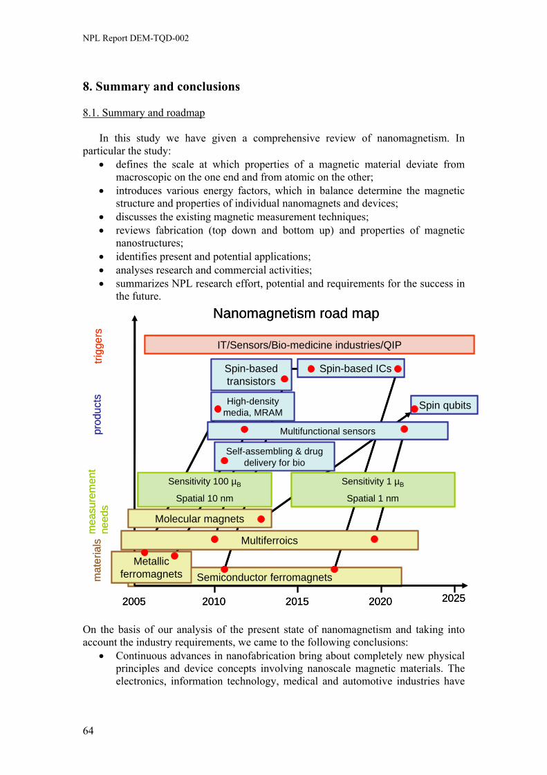
NPL Report DEM-TQD-002
8. Summary and conclusions 8.1. Summary and roadmap
In this study we have given a comprehensive review of nanomagnetism. In particular the study:
• defines the scale at which properties of a magnetic material deviate from macroscopic on the one end and from atomic on the other;
• introduces various energy factors, which in balance determine the magnetic structure and properties of individual nanomagnets and devices;
• discusses the existing magnetic measurement techniques; • reviews fabrication (top down and bottom up) and properties of magnetic
nanostructures; • identifies present and potential applications; • analyses research and commercial activities; • summarizes NPL research effort, potential and requirements for the success in
the future.
Semiconductor ferromagnets
Nanomagnetism road map
2005 2015 2020 20252010
mat
eria
lspr
oduc
tstri
gger
sm
easu
rem
ent
need
s
IT/Sensors/Bio-medicine industries/QIP
Multifunctional sensors
High-density media, MRAM
Self-assembling & drug delivery for bio
Sensitivity 1 µB
Spatial 1 nm
Sensitivity 100 µB
Spatial 10 nm
Multiferroics
Molecular magnets
Metallic ferromagnets
Spin qubits
Spin-based transistors
Spin-based ICs
Semiconductor ferromagnets
Nanomagnetism road map
trigg
ers
IT/Sensors/Bio-medicine industries/QIP
2005 2015 2020 20252010
mat
eria
lspr
oduc
tsm
easu
rem
ent
need
s
Multifunctional sensors
Spin-based transistors
Spin-based ICs
High-density media, MRAM
Self-assembling & drug delivery for bio
Sensitivity 1 µB
Spatial 1 nm
Sensitivity 100 µB
Spatial 10 nm
Multiferroics
Molecular magnets
Metallic ferromagnets
Spin qubits
On the basis of our analysis of the present state of nanomagnetism and taking into account the industry requirements, we came to the following conclusions:
• Continuous advances in nanofabrication bring about completely new physical principles and device concepts involving nanoscale magnetic materials. The electronics, information technology, medical and automotive industries have
64
NPL Report DEM-TQD-002
become increasingly interested in utilizing these materials and are actively involved in research and development.
• An important R&D trend is that it is no longer enough to demonstrate purely magnetic properties of a material. For a successful application the material or device should often possess multifunctional properties, e.g. combination of ferromagnetic and piezoelectric properties or possibility to operate the magnetic state by an electric field.
• Modern industry, being understandably conservative in their commitment to semiconductors, is especially interested in combining semiconducting and magnetic properties in a single material. We conclude that DMS-based materials have the potential to promote true spintronics revolution within 10 years. The prerequisite for this will be the demonstrable ferromagnetism in combination with semiconducting properties in one material (preferably group IV-based) at room temperature and above. Recent NPL-Cork work indicates how this breakthrough can be achieved in a GeMn nanowire.
• Magnetic nanocomposites (especially laminar) and multilayered (e.g., ferromagnetic-piezoelectric) materials will become increasingly important in sensors and magnetic memory devices.
• Emerging technologies have their share of interest in nanomagnetism. Magnetic molecules and S-F-S Josephson junctions are of particular interest to quantum information processing, which may become technically possible within the next 15 years.
• Metallic nanomagnets will retain their central position in magneto-transport applications based on the GMR and TMR effects (therefore, keeping their position in sensor applications) and will certainly continue to be used in basic research.
• Magnetic measurements: magnetisation measurement techniques are very well established.
Sensitivity close to 1 μB has been demonstrated, albeit in a rather special material. This class of methods will remain crucial for material and device characterisation;
magnetic microscopy and time-resolved magnetic measurements are rapidly developing;
combining spatial and temporal resolution with magnetic sensitivity is a challenge for the future.
The pace at which the field of nanomagnetism is changing almost guarantees that the above assessment will soon require significant alteration. However, it looks certain that the overall vector of development towards increasing integration of the magnetic nanomaterials into various electronic devices will be sustained. By the same token nanomagnetic metrology will become increasingly important.
Particular observations of this study regarding the R&D activity in nano-magnetism are:
• The R&D community in this topic is truly international: it includes the UK, the EU, Japan and the USA.
• Research groups are spread over academic, government, including defence, and commercial institutions. Examples outside of academia include NIST, NTT, Intel, and Hitachi.
65

NPL Report DEM-TQD-002
• Existing European Union projects in this area have a total value of about €58M, with the EU contribution being about €40M.
These activities are described in the report. They illustrate that organisations outside of academia are intensely investing in nanomagnetism R&D.
As evident from responses to our questionnaire, metrology is considered to be the cornerstone of the scientific progress and commercial success of nanomagnetism.
8.2. Conclusions and recommendations NPL entered the field of nanomagnetism relatively recently, but has already managed to demonstrate a good level of research. In particular it concerns the study of magnetic nanoparticle arrays, nanowires, magnetic molecules, but most of all, diluted magnetic semiconductors (DMS). Leading industrial companies (see Questionnaire, Section 7) identify the critical role of metrology in the investigation and reliable classification of novel materials that could provide new spin functions as well as in improving materials and interface properties at the nanometer scale. As device concepts are evaluated, nanometer scale spin metrology will be crucial to understand different aspects of the device operation and will allow for optimising device fabrication processes. Therefore, the central role for NPL is to develop the precise and reliable measurement technique of magnetic properties on the nanoscale which underpin the industrial research.
• We recommend to expand our research in the field of DMS by including new types of hybrid structures, in particular ferromagnetic-piezoelectric and multiferroics, with the aim of controlling the magnetic anisotropy by electrostriction in a hybrid structure on the nanoscale. A successful demonstration will impact on the development of a new generation of high-density magnetic storage devices that do not require heat or high electric current.
• Research on DMS nanowires and nanocables is aimed towards demonstrating their feasibility as the building blocks of electronics of the ‘post-CMOS’ era. Recent NPL results which demonstrated room temperature ferromagnetism in GeMn nanowires certainly encourages research in this direction. These results were very well received by the research and industrial communities. We recommend to continue this successful research by studying the physical mechanism underlying the anomalously high Curie temperature and to correlate the magnetic and electric properties of the wires. This will be supported by the newly appointed Strategic Research Fellow in molecular modelling.
• We suggest to continue our work on magnetic molecules. We intend to study magnetisation tunnelling in Mn12 in the view of their potential as qubit devices and in the emerging field of molecular electronics. This objective addresses a long-term aim of the Quantum Programme by investigating technologies which could be important on the 15 year time scale. In particular, devices based on molecular magnets represent an alternative approach to the qubit realization which is the key issue in Quantum Information Processing and is closelyrelated to the existing and future NPL activity in the area (see NPL Report on ‘Applications of Quantum Entanglement to Metrology’).
• Enhancing our existing magnetic characterisation capabilities and techniques is an essential part of our work program:
66
NPL Report DEM-TQD-002
In particular, we need to continue the development of the tuning fork-based low temperature AFM/MFM system. This facility along with thework on spin detection using SQUIDs will allow us to detect single spins on the nanometer level scale, i.e. realise ‘1 μB - 1 nm’ metrology.
A sensitive variable temperature magnetometer - an essential tool in any magnetic characterisation, is a ‘must have’. The strong tendency to study and use multifunctional materials suggests that the new kit should allow for magnetic moment to be measured simultaneously with other physical properties: electric, thermal, etc.
We believe that NPL has the potential to become a key player in nanomagnetic metrology. Our existing extensive collaboration network covers manufacturers of magnetic samples, groups performing nanofabrication, structural analysis, dynamic magnetic measurements, as well as potential end-users of nanomagnetic devices, such as Intel and NTT. However, we have not yet reached the ‘critical mass’ of researchers at NPL sufficient for the diversity and complexity of tasks. This situation should be addressed on the management level.
67
NPL Report DEM-TQD-002
9. Appendix A 9.1. UK Academia (examples) Imperial College
• Current expertise and interest in nanomagnetism The main research interest is highly spin-polarised ferromagnets, dilute magnetic
semiconductors (mostly oxides) and functional magnetic materials such as giant magnetocaloric materials. The research is aimed to determine the degree of spin polarisation of the transport current and reach an ability to control properties so that these materials can be used as high resolution sensors and hybrid spintronic devices. The Physics Department has several programs (jointly with the Materials Department of Cambridge University and Surrey University): to develop magnetic oxide metals and semiconductors, to control the interfaces between ferromagnets and semiconductors and to create planar arrays of Andreev junctions to look at spin polarisation spatially.
• Funding Overall these programs fund the Imperial work to a total of £1.1M. The European
Union, the EPSRC and also NPL finance the research. • People
There are currently 5 research assistants and 2 PhD students involved. • Facilities - Two magnetometers (8 T vertical field and a 5 T split pair with 300 K to 4.2 K
continuous flow cryostat inserts); - Micro-calorimetry with the same temperature and field range; - Point contact Andreev reflection spectroscopy and its LT STM version for
higher spatial resolution; - Scanning Hall magnetotometry and imaging down to 20 K; - Room temperature MFM; - Range of magnetotransport probes for conductivity and Hall experiments
spanning from 300 K (8 T) to 300 mK (4 T); - Access to high resolution Kerr magnetometry, scanning Raman microscopy
and ellipsometry. • Collaboration
IMEC, Toshiba, NEC, Seagate, QinetiQ • Expectations and the future research on nanomagnetism
Growth areas will be in the digital electronics end, including the domain wall nanostructures and magnetooresistance devices for biological applications.
• Role of metrology Metrology is important at the nanoscale but clearly new tools for metrology at this
level are strongly required. Southampton University
• Current expertise and interest in nanomagnetism - Novel fabrication methods: electrochemical deposition in self-assembled
templates with feature sizes 2 – 2000 nm; - Hybrid nanomagnetic and Si-SiO2 structures. Guided self-assembly template
methods;
68
NPL Report DEM-TQD-002
- Epitaxial magnetic nanostructures. Multilayers of different magnetic materials: rare earth based magnets, hard-soft composite systems, exchange spring systems, spintronics, novel prototype recording schemes;
- Computational modelling of nanomagnetic systems. Development of software suite for micromagnetic modelling.
• Funding Funding through EPSRC (ca £500K per year), Qinetiq Ltd, University of Southampton (E-Science Initiative, SRIF), Merck Ltd.
• People - Physics: 2 staff, 2 PDRAs, 4 postgrads; - Chemistry: 1 staff, 1 postgrad; - Computational Engineering Group (Engineering Sciences): 1 staff, 1 PDRA, 3
postgrads; - Electronics and Computer Sciences: 1 staff, 3 postgrads. • Facilities - Magnetometers, fields up to 16 T, 0.3 K<T<300 K (SQUID, VSM, Hall
probe); - Transport and susceptibility rigs, fields up to 16 T, 0.3 K<T<300 K, angular
control 0.001°; - Specific heat rig; - Magneto-optical Kerr effect; - MFM (under development); - Structural characterisation: SEM, AFM; - Electrochemical characterisation. • Collaboration
Qinetiq Ltd, Nanotecture Ltd. • Expectations and the future research on nanomagnetism The nanomagnetism field driven by the potential for applications and novel
physics will grow both generally (worldwide) and at Southampton, at least for the next 10 years. Developments beyond 10 years depend strongly on the success of this research in pushing the super-paramagnetic limit in data-storage and in the coming to market of currently-emerging nanomagnetic technologies (bio-applications etc.).
Areas of the future research for Southampton Univ. are pushing length scales below 10 nm, quantum effects and functionalities, spin transport devices.
The amount of funding will determine the breadth of the programme at Southampton. About £500k p.a. would allow an internationally leading programme on these topics to blossom.
• Role of metrology Standard characterisation is best done in-house but the following would be great if
it would be available to the UK community: - Spin polarised STM; - Fast (microwave) electronics to study the dynamics and excitations (spin
transfer torque, switching, etc.). University of Glasgow
• Current expertise and interest in nanomagnetism The main expertise is in fabrication of small magnetic structures by e-beam
lithography (EBL) and focused ion beam (FIB) techniques and characterization of the resulting structures by analytical electron microscopy and high resolution magnetic
69
NPL Report DEM-TQD-002
imaging. The goal is to understand the interplay between physical and magnetic properties, with a view to realising structures with functionalised properties.
Main project is to push size limits down using EBL and FIB; also have activity involving domain wall manipulation in elements.
• Funding Mainly EPSRC but some funding from EU and support from Seagate.
• People 2 staff members, 3 post-docs and 3 research students, although not full time involvement.
• Facilities - High resolution analytical electron microscopy (emphasis on probe modes,
especially EELS); - Magnetic imaging using Lorentz microscopy and MFM. • Collaboration
Seagate, Siemens (to a small extent). • Expectations and the future research on nanomagnetism Increased role in high density storage; very exciting new possibilities if
spintronics takes off. Within this road-mapping the group will start a project as part of Spintronics
Consortium in 2006. The funding required for the activity is ca £400k per year. • Role of metrolog. Important in realising structure/devices with reproducible properties.
9.2. Commercial activity (examples) Intel
• Current expertise and interest in nanomagnetism The International Technology Roadmap for Semiconductors (ITRS) has identified
that “exotic” new devices may need to be integrated with CMOS beyond ~2018 and includes spin based devices in the options. Intel is interested in evaluating the potential of spin based devices as they are a proposed future alternative to conventional charge based transistors. We regard these devices as “exotic” as we imagine they will be quite different in terms of their operation, structure, and material composition compared to conventional charge-based transistors. As such we are interested in semiconductor spintronics and ferromagnetic semiconductor materials, structures (e.g. magnetic nanowires), and novel spin materials (such as magnetoelectric and multiferroic) to enable new functionality of these alternative devices. We believe significant material research (synthesis, metrology and characterisation, and modelling) is required to realise such “exotic” devices. Intel evaluates various nanomagnetic materials, device structures, and characterisation techniques for “exotic” device applications, and has several projects running all around the world – largely in collaboration with industry research consortia, governments, and research institutes / academia.
• Funding For example, Science Foundation Ireland (SFI) is funding the research in Ireland through the CRANN (Centre for Research in Adaptive Nanostructures and Nanodevices) CSET (Centre for Science Engineering and Technology), which covers many nanoscience themes, one of which concerns spintronics.
- CRANN is funded with €21M from SFI and €5M from private donations.
70
NPL Report DEM-TQD-002
- Other SFI grants include a €5M principal investigator grant for the CINSE (Conception and Implementation of Nanoscale Spin Electronics) project from 2001-2006.
• People About 10 post-docs and 12 PhD and M.Sc. students are working in the magnetics
group in Trinity College Dublin for CRANN and CINSE. • Facilities
X-ray diffraction, SQUID magnetometer, VSM, Mössbauer spectroscopy, magnetoresistance/transport vs. temperature, Magneto-Optic Kerr Effect.
• Collaboration - CRANN is an industrial/academic partnership between Trinity College
Dublin, University College Dublin, University College Cork, with Intel Ireland as the primary industrial partner.
- Intel is very interested in working collaboratively with universities, research institutes, other industries, and governments to progress scientific understanding and associated technological challenge for devices beyond CMOS, i.e. “exotic” devices based on state variables other than charge.
• Expectations and the future research on nanomagnetism - In the near term (~5-10 years), Intel expects that the magnetic storage
industry will begin to exploit ‘exotic’, e.g. spin-based, devices to increase hard disk memory densities
- In 5 years the semiconductor industry will evaluate the potential of spin transistors as successors to conventional transistor technology. This will involve an understanding of the associated materials and device structures.
- If spin devices are viable alternatives to conventional charge-based transistors with clear advantages in cost, power consumption, and future scaling, companies in the semiconductor industry could bring them in-house for research and development towards high volume manufacturing in the next 10-15 years.
• Role of metrology Metrology will be critical to identify materials that could provide new spin functions (such as gain, low dissipation transport) and improve the materials and interface properties at the nanometer scale. As device concepts are evaluated, nanometer scale spin metrology will be critical to understand the operation of materials, interfaces and transport mechanisms within the device and then improve device fabrication processes to improve operation.
Hitachi Cambridge Laboratory
• Current expertise and interest in nanomagnetism - Electrical generation and optical detection as well as optical generation and
electrical detection of spin-polarization in nonmagnetic semiconductor (SC) heterostructures with reduced dimensionality (e.g. spin Hall effect in 2D-hole gas, Anomalous Hall effect in 2D electron gas);
- Current induced spin-polarization in systems with broken inversion symmetry);
- Hybrid ferromagnetic metal - SC structures with reduced dimensions, such as magnetostatically gated quantum dots;
- Submicron patterned structures from ultrathin diluted magnetic semiconductor (DMS) films (e.g. GaMnAs), such as nano-contact magnetoresistance device;
71

NPL Report DEM-TQD-002
- Spin injection and accumulation in 0D nanomagnets; - Spin transfer toque phenomena in magnetic nanopillars; - Study of magnetic domain walls in patterned stripes fabricated from both
ferromagnetic metal multilayer systems and DMS films; - Spin-injection into carbon nanotubes. • Funding
Currently no fund beside Hitachi internal fund. • People
8 people including pos-doc and PhD students. • Facilities - High resolution SEM; - High resolution Kerr microscope from low temperature to RT; - Cryogenic equipment for magnetotransport measurements at ultralow
temperatures (<50 mK) and strong magnetic fields (16 T) such as various cryostats and dilution refrigerators;
- Cryogenic equipment with optical access and magnetic fields (temperature range from room temperature down to 1.5 K, magnetic field up to 6 T);
- Ultrafast optical pump-probe systems. • Collaboration Hitachi is collaborating with different universities and research organizations depending on the project. In particular,
- University of Cambridge, UK; - National Physical Laboratory, UK; - Nottingham University, UK; - Leeds University, UK; - Texas A&M University, USA; - Institute of Physics ASCR, Czech Republic; - University of Paris Sud, France.
• Expectations and the future research on nanomagnetism General trend: In 5 years, nanomagnetism on the current metallic ferromagnets
will be the most important topic. It is also very important to development of patterned media, magnetic heads with ultra-high resolution and memory cells for MRAMs. During 10 and 20 years, nanomagnetism on semiconductor materials including both pure and diluted ferromagnetic semiconductors will be the major topics. Hitachi plans: In 5 years, nanomagnetism in both metal and SC ferromagnets will be the main research target. During 10 and 20 years, nanomagnetism on semiconductor materials will be the prime research targets.
NTT Basic Research Laboratories (BRL)
• Current expertise and interest in nanomagnetism NTT BRL has the spintornics group which is mainly working in three areas of
nanomagnetism: - Spin current transport through ferromagnet/semiconductor (FM/SC)
junctions. FM/SC junctions have a gate electrode attached on the SC region and the spin current through M/SC junctions can be controlled by gate voltage;
- Realization of ferromagnetism using artificial crystals which do not contain any magnetic materials. According to theoretical analysis, if artificial atoms have the structure like Kagome lattice and related lattice structures, they
72

NPL Report DEM-TQD-002
have a flat-band structure in their band diagram at certain conditions, which naturally gives ferromagnetism due to the number difference between up spins and down spins in the lattice;
- nano-SQUID project. Nano-SQUID project seeks ultimate magnetic sensitivity like detecting one flip of a spin using a nano-size SQUID.
• Funding Mainly by NTT Europe Basic Research Laboratory. Additional funding from
collaborative projects with NPL and Royal Holloway University of London. • People
Three people (UK branch). • Facilities
Dilution refrigerators, SEMs, and AFM. • Collaboration
Royal Holloway University of London, NPL. • Expectations and the future research on nanomagnetism - During 5 years: ultra-dense magnetic memory media; - During 10 years: spin transistors; - During 20 years: spin qubits. • Role of metrology A possibility to detect and manipulate very small magnetic fields, in order of a
few Bohr magneton, is crucial for nanomagnetism. It requires both precise measurement techniques and a novel methodological approach.
73

NPL Report DEM-TQD-002
10. Glossary AAO – anodised aluminium oxide AGM - alternating gradient magnetometer AF - antiferromagnetic AFM - atomic force microscopy BETS – bis(ethylenedithio)tetraselenafulvalene BCS theory - Bardeen-Cooper-Schrieffer theory CMOS – complementary metal oxide semiconductor CPR - current-phase relationship 2DEG - two-dimensional electron gases DMS – diluted magnetic semiconductor DOS - density of states EB - exchange bias ESR - electron spin resonance FRAM - ferroelectric random access memory FM - ferromagnetic GMR - giant magnetoresistance sensors HS - high spin LDA – local density approximation LED – light emitting diod LOFF state - Larkin-Ovchinnikov-Fulde- Ferrel state LS - low spin MDM - magnetic dissipation microscopy ME – magnetoelectric MEMS - micro-electromechanical systems MFM - magnetic force microscope MOKE – magneto-optical Kerr effect MRAM - magnetic random access memory MRFM - magnetic resonance force microscopy MRI - magnetic resonance imaging MSM - magnetoresistance sensitivity mapping PZT - lead zirconate titanate (PbZr1−xTixO3) RKKY interaction - Ruderman–Kittel–Kasuya–Yosida interaction SCF - supercritical fluid SEMPA - scanning electron microscopy with polarization analysis SF - superconductor – ferromagnet SFS - superconductor – ferromagnet – superconductor SN - superconductor – normal SPICE - spin-polarized-injection current emitter SP-STM - spin-polarized scanning tunneling microscope SQUID - Superconducting Quantum Interference Device STNO - spin torque nano-oscillator TCNE - tetracyanoethenide VSM - vibrating sample magnetometer XMCD - x-ray magnetic circular dichroism
74

NPL Report DEM-TQD-002
11. References 1 T. Hayashi, Sh. Hirono, M. Tomita, and Sh. Umemura, Nature 382, 772 (1996).
2 R. L. Comstock. Introduction to Magnetism and Magnetic Recording (New York: Wiley, 1999).
3 K. J. Kirk. Contemp, Phys. 41, 61 (2000).
4 D. J. Sellmyer, C. P. Luo, Y. Qiang, and J. P. Liu, Nanomaterials and magnetic thin films in Handbook of Thin
Film Materials vol 5, ed. H. S. Nalwa (San Diego, CA: Academic) p. 337 (2002).
5 See e.g. M. Ziese and M. J. Thornton, Spin Electronics (Berlin: Springer, 2001).
6 J. S. Parker, S. M. Watts, P.G. Ivanow, and P. Xiong, Phys. Rev. Lett., 88, 196601 (2002).
7 I. I. Oleinik, E. Y. Tsymbal and D. G. Pettifor, Phys. Rev. B 62, 3952 (2000).
8 M. Hunziker and M. Landolt, Phys. Rev. Lett. 84, 4713 (2000).
9 T. C. Schulthess and W. H. Butler, J. Appl. Phys. 89, 7021 (2001).
10 R. Fiederling, M. Keim, G. Reuscher, W. Ossau, G. Schmidt, A. Waag, and L. W. Molenkamp, Nature, 402, 787 (1999).
11 P. Van Dorpe, W. Van Roy, V. F. Motsny, G. Borghs, and J. De Boeck. J. Vac. Sci. Technol. A 22, 1862 (2004).
12 R. P. Cowburn and M. E. Welland, Science 287, 1466 (2000).
13 S. Wolf and T. Curcic, Physics World, N7, 21 (2005).
14 R. Hanson, L. H. Willems van Beveren, I. T. Vink, J. M. Elzerman, W. J. M. Naber, F.H. L. Koppens, L. P. Kouwenhoven,
and L. M. K. Vandersypen, Phys. Rev. Lett. 94, 196802 (2005).
15 H.-A. Engel and D. Loss. Science 309, 586 (2005).
16 S. Murakami, N. Nagaosa, and S.-C. Zhang, Science, 301, 1348 (2003).
17 P. Grünberg, R. Schreiber, Y. Pang, M. B. Brodsky, and H. Sowers, Phys. Rev. Lett. 57, 2442 (1986).
18 M. N. Baibich, J. M. Broto, A. Fert, F. Nguyen Van Dau, F. Petroff, P. Etienne, G. Creuzet, A. Friederich, and J.
Chazelas, Phys. Rev. Lett. 61, 2472 (1988).
19 S. S. P. Parkin, Phys. Rev. Lett. 67, 3598 (1991).
20 See e.g. J. M. D. Coey, A. E. Berkowitz, L. Balcells, F. F. Putris, and A. Barry, Phys. Rev. Lett. 80, 2815 (1998).
21 J. M. D. Coey and M. Venkatesan, J. Appl. Phys. 91, 8345 (2002).
22 J. M. D. Coey, M. Venkatesan, C. B. Fitzgerald, Nature Materials 4, 173 (2005).
23 C. C. Berry and A. S. G. Curtis, J. Phys. D: Appl. Phys. 36, R198 (2003).
24 K. O’Grady (ed), J. Phys. D: Appl. Phys. 36, 165 (2003).
25 J. M. Perez, J. Am. Chem. Soc. 125, 10192 (2003).
26 P. A. Dowben, Surf. Sci. Rep. 40, 151 (2000).
27 O. Kazakova, M. Hanson and A. C.C. Yu, J. Appl. Phys. 96, 6512 (2004).
28 K.-H. Fischer and A. J. Hertz, Spin Glasses (Cambridge: Cambridge University Press, 1991).
29 L. M. Sandratskii, Phys. Rev. B 64, 134402 (2001).
30 E. M. Chudnovsky, W. M. Saslow and R. A. Serota, Phys. Rev. B 33, 251 (1986).
31 R. Coehoorn, D. B. de Mooij, J. P. W. B. Duchateau and K. H. J. Buschow, J. Physique Coll. 49, 669 (1988).
32 R. Skomski, J. Appl. Phys. 83, 6503 (1998).
33 R. Skomski, J. P. Liu and D. J. Sellmyer, Phys. Rev. B 60, 7359 (1999).
34 R. Skomski, J. P. Liu, J. M. Meldrim, and D. J. Sellmyer, Magnetic Anisotropy and Coercivity in Rare-Earth Transition Metal
Alloys ed. L. Schultz and K.-H .Müller (Frankfurt/M: Werkstoffinformationsgesellschaft, 1998) p 277.
35 G. C. Hadjipanayis, J. Magn. Magn. Mater. 200, 373 (1999).
36 J. P. Liu, R. Skomski, Y. Liu and D. J. Sellmyer, J. Appl. Phys. 87, 6740 (2000).
37 D. Givord and M. F. Rossignol, Rare-Earth Iron Permanent Magnets ed. J. M. D. Coey (Oxford: Oxford University Press,
1996), p. 218.
38 H. Kronmüller, Phys. Status Solidi b 144, 385 (1987).
39 H. Kronmüller, K.-D. Durst and M. Sagawa, J. Magn. Magn. Mater. 74, 291 (1988).
40 W. F. Brown, Micromagnetics (New York: Wiley, 1963).
41 E. C. Stoner and E. P. Wohlfarth, Phil. Trans. R. Soc. A 240, 599 (1948).
75

NPL Report DEM-TQD-002
42 A. Aharoni, Rev. Mod. Phys. 34, 227 (1962).
43 L. D. Landau and E. M. Lifshitz, , Phys. Z. Sowjetunion, 8, 153 (1935). 44 T.L. Gilbert, Phys. Rev. 100, 1243 (1955). 45 S. Foner, J. Appl. Phys. 79, 4740 (1996).
46 H. Zijlstra, Experimental Methods in Magnetism vol. 2 (Amsterdam: North Holland, 1987).
47 L. Peterson and A. Ehrenberg, Rev. Sci. Instrum. 56, 575 (1985).
48 P. J. Flanders, J. Appl. Phys. 63, 3940 (1988).
49 C. Ascoli, P. Baschieri, C. Frediani, L. Lenci, M. Martinelli, G. Alzetta, R. M. Celli, and L. Pardi, Appl. Phys. Lett. 69, 3920
(1996).
50 E. Arimondo, Nuovo Cimento B 52, 379 (1967).
51 G. Alzetta, E. Arimondo, C. Ascoli, and A. Gozzini, Paramagnetic resonance detection at low fields with angular momentum
detection Nuovo Cimento B, 52 392 (1967).
52 C. Lupien, B. Ellman, P. Grutter, and L. Taillefer, Appl. Phys.Lett. 76, 3564 (2000).
53 M. Willemin, C. Rossel, J. Brugger, M. H. Despont, H. Rothuizen, P. Vettiger, J. Hofer, and H. Keller, J. Appl. Phys. 83,
1163 (1998).
54 J. G. E. Harris, D. D. Awschalom, F. Matsukura, H. Ohno, K. D. Maranowski, and A. C. Gossard, Appl. Phys. Lett. 75, 1140
(1999).
55 M. P. Schwarz, D. Grundler, I. Meinel, Ch. Hey,n and D. Heitmann, Appl. Phys. Lett. 74, 451 (1999).
56 J. G. E. Harris, D. D. Awschalom, K. D. Maranowski, and A. C. Gossard, J. Appl. Phys. 87, 5102 (2000).
57 J. W. Judy, H. Yang, P. Irazoqui-Pastor, K. Yang, N. Myung, M. Schwartz, and K. Nobe, Tech. Dig. Solid-State Sensor and
Actuator Workshop (Hilton Head Island, SC, June 4–8, 2000).
58 J. Morrillo, Q. Su, B. Panchapakesan, M. Wuttig, and D. Novotny, Rev. Sci. Instrum. 69, 3908 (1998).
59 S. J. Barnett, Rev. Mod. Phys. 7, 129 (1935).
60 M. Löhndorf, J. Moreland and P. Kabos, Appl. Phys. Lett. 76, 1176 (2000).
61 Y. Martin, H. K. Wickramasinghe, Appl. Phys. Lett. 50, 1455 (1987).
62 J. J. Saenz, N. García, P. Grütter, E. Meyer, H. Heinzelmann, R. Wiesendanger, L. Rosenthaler, H. R. Hidber, and H.-J.
Güntherodt, J. Appl. Phys. 62, 4293 (1987).
63 H. J. Hug, B. Stiefel, P. J. A. van Schendel, A. Moser, R. Hofer, S. Martin, H.-J. Güntherodt, S. Porthun, L. Abelmann, J. C.
Lodder, G. Bochi, and R. C. O'Handley, J. Appl. Phys. 83, 5609 (1998).
64 P. Grütter, Y. Liu, P. LeBlanc, U. Dürig, Appl. Phys. Lett. 71, 279 (1997).
65 J. A. Sidles, J. L. Garbini, K. J. Bruland, D. Rugar, O. Züger, S. Hoen, and C. S. Yannoni, Magnetic resonance force
microscopy Rev. Mod. Phys. 67, 249 (1996).
66 H. J. Mamin, R. Budakian, B. W. Chui, and D. Rugar, Phys. Rev. B 72, 024413 (2005).
67 D. Rugar, R. Budakian, H. J. Mamin, and B. W. Chui, Nature 430, 329 (2004). 68 S. McVitie, J. N. Chapman, L. Zhou, L. J. Heyderman and W. A. P. Nicholson, J. Magn. Magn. Mat. 148, 232 (1995).
69 K. J. Kirk, J. N. Chapman, S. McVite, P. R. Aitchison, C. D. W. Wilkinson, Appl. Phys. Lett. 75, 3683 (1999).
70 A. M. Chang, H. D. Hallen, L. Harriott, H. F. Hess, H. L. Kao, J. Kwo, R. E. Miller, R. Wolfie, J. van der Ziel, and T. Y.
Chang, Appl. Phys. Lett. 61, 1974 (1992).
71 J. R. Kirtley, M. B. Ketchen, K. G. Stawiasz, J. Z. Sun, W. J. Gallagher, S. H. Blanton, and S. J. Wind, Appl. Phys. Lett. 66,
1138 (1995).
72 H. J. Williams, F. G. Foster, E. A. Wood, Phys. Rev. 82, 119 (1951).
73 B. E. Argyle and J. G. McCord, J. Appl. Phys. 87, 6487 (2000).
74 C. T. Chen, Y. U. Idzerda, H.–J. Lin, G. Meigs, A. Chaiken, G. A. Prinz, and G. H. Ho, Phys. Rev. B 48, 642 (1993).
75 J. M. Tonnerre, L. Sève, D. Raoux, G. Soullié, B. Rodmacq, and P. Wolfers, Phys. Rev. Lett. 75, 740 (1995).
76 T. P. A. Hase, I. Pape, B. K. Tanner, H. Dürr, E. Dudzik, G. van der Laan, C. H. Marrows, and B. J. Hickey, Phys. Rev. B 61,
R3792 (2000).
77 H. A. Dürr, E. Dudzik, S. S. Dhesi, J. B. Goedkoop, G. van der Laan, M. Belakhovsky, C. Mocuta, A. Marty, and Y. Samson,
Science 284, 2166 (1999).
76
NPL Report DEM-TQD-002
78 N. Ishimatsu, H. Hashizume, S. Hamada, N. Hosoito, C. S. Nelson, C. T. Venkataraman, G. Srajer, and J. C. Lang, Phys. Rev.
B 60, 9596 (1999).
79 C. H. Marrows, P. Steadman, A. C. Hampson, L.-A. Michez, B. J. Hickey, N. D. Telling, D. A. Arena, J. Dvorak, and S.
Langridge. Phys. Rev. B 72, 024421 (2005).
80 C. Spezzani, M. Fabrizioli, P. Candeloro, E. Di Fabrizio, G. Panaccione, and M. Sacchi, Phys. Rev. B 69, 224412 (2004).
81 T. Duden and E. Bauer, Phys. Rev. B 59, 474 (1999).
82 R. Wiesendanger, H.-J. Güntherodt, G. Güntherodtt, R. J. Gambino, R. Ruf, Phys. Rev. Lett. 65, 247 (1990).
83 M. Johnson and J. Clarke, J. Appl. Phys. 67, 6141 (1990).
84 S. F. Alvarado, J. Appl. Phys. 73, 5816 (1993).
85 W. K. Hiebert, A. Stankiewicz, M. R. Freeman, Phys. Rev. Lett. 79, 1134 (1997).
86 B. C. Choi, M. Belov, W. K. Hiebert, G. E. Ballentine, and M. R. Freeman, Phys. Rev. Lett. 86, 728 (2001).
87 T. M. Crawford, T. J. Silva, C. W. Teplin, and C. T. Rogers, Appl. Phys. Lett. 74, 3386 (1999).
88 J. J. Reif, J. C. Zink, C. M. Schneider, J. Kirschner, Phys. Rev. Lett. 67, 2878 (1991).
89 F. Sirotti, R. Bosshard, P. Prieto, G. Panaccione, L. Floreano, A. Jucha, J. D. Bellier, and G. Rossi, J. Appl. Phys. 83, 1563
(1998).
90 M. Bonfim, G. Ghiringhelli, F. Montaigne, S. Pizzini, N. B. Brookes, F. Petroff, J. Vogel, J. Camarero, and A. Fontaine, Phys.
Rev. Lett. 86, 3646 (2001).
91 S. Wildermuth, S. Hofferberth, I. Lesanovsky, E. Haller, L. M. Andersson, S. Groth, I. Bar-Joseph, P. Kruger, and J.
Schmiedmayer, Nature, 435, 440 (2005).
92 J. M. Kikkawa and D. D. Awschalom, Nature 397, 139 (1999).
93 K. Nakamura, H. Hasegawa, T. Oguchi, K. Sueoka, K. Hayakawa, and K. Mukasa, Phys. Rev. B 56, 3218 (1997).
94 D. Rugar, C. S. Yannoni, and J. A. Sidles, Science 264, 1560 (1994).
95 F. J. Himpsel, J. E. Ortega, G. J. Mankey, and R. F. Willis, Adv. Phys. 47, 511 (1998).
96 U. Gradmann, Handbook of Magnetic materials vol. 7, ed. K. H. J. Buschow (Amsterdam: Elsevier, 1993) p 1.
97 D. Sander, R. Skomski, C. Schmidthals, A. Enders, and J. Kirschner, Phys. Rev. Lett. 77, 2566 (1996).
98 D. Sander, Rep. Prog. Phys. 62, 809 (1999).
99 J. A. C. Bland and B. Heinrich (ed) Ultrathin Magnetic Structures vol 1 (Berlin: Springer, 1994).
100 S. Blügel, Phys. Rev. B 51, 2025 (1995).
101 J. Ferré J, J. P. Jamet and P. Meyer, Phys. Status Solidi a 175, 213 (1999).
102 M. Bander and D. L. Mills, Phys. Rev. B 38, 12015 (1988).
103 G. J. Bowden, J. M. L. Beaujour, S. Gordeev, P. A. J. de Groot, B. D. Rainford, and M. Sawicki, J. Phys.: Condens.
Matter 12, 9335 (2000).
104 M. Sawicki, G. J. Bowden, P. A. J. de Groot, B. D. Rainford, J. M. L. Beaujour, R. C. C. Ward, and M. R. Wells,
Phys. Rev. B 62, 5817 (2000).
105 J.I. Martin, J. Nogues, K. Liu, J.L. Vicent, and I. K. Schuller, J. Magn. Magn. Mater. 256, 449 (2003).
106 K. Bessho, Y. Iwasaki, S. Hashimoto, J. Appl. Phys. 79, 5057 (1996).
107 S. Wirth, S. von Moln!ar, M. Field, and D.D. Awschalom, J. Appl. Phys. 85, 5249 (1999).
108 A.D. Kent, T.M. Shaw, S. von Molnar, and D.D. Awschalom, Science 262, 1249 (1993).
109 W. Schindler, D. Hofmann, J. Kirshner, J. Appl. Phys. 87, 7007 (2000).
110 S.Y. Chou, P.R. Krauss, L. Kong, J. Appl. Phys. 79, 6101 (1996).
111 B. Cui, L. Kong, X. Sun, and S.Y. Chou, J. Appl. Phys. 85, 5534 (1999).
112 S.Y. Chou, P.R. Kraus, W. Zhang, L. Guo, and L. Zhuang, J. Vac. Sci. Technol. B 15, 2897 (1997).
113 P. Ohresser, G. Ghiringhelli, O. Tjernberg, N.B. Brookes, and M. Finazzi, Phys. Rev. B 62, 5803 (2000).
114 K.L. Lee, R.R. Thomas, A. Viehbeck, and E.J.M. O’Sullivan, J. Vac. Sci. Technol. B 11, 2204 (1993).
115 S. Sun, C.B. Murray, D. Weller, L. Folks, and A. Moser, Science 287, 1989 (2000).
116 C.T. Black, C.B. Murray, R.L. Sandstrom, and S. Sun, Science 290, 1131 (2000).
117 K. Liu, S.M. Baker, M. Tuominen, T.P. Russell, I.K. Schuller, Phys. Rev. B 63, 060403 (2001).
118 T. Thurn-Albercht, J. Schotter, G.A. Kastle, N. Emley, T. Shibauchi, L. Krusin-Elbaum, K. Guarini, C.T. Black, M.T.
Tuominen, and T.P. Russell, Science 290, 2126 (2000).
77

NPL Report DEM-TQD-002
119 S.P. Li, W.S. Lew, Y.B. Xu, A. Hirohata, A. Samad, F. Baker, and J.A.C. Bland, Appl. Phys. Lett. 76, 748 (2000).
120 W.D. Williams, N. Giordano, Phys. Rev. B 33, 8146 (1986).
121 G.E. Thompson, R.C. Furneaux, G.C. Wood, J.A. Richardson, and J.S. Gode, Nature 272, 433 (1978).
122 D. J. Sellmyer, M. Zheng, and R. Skomski, J. Phys.: Condens. Matter. 13, R433 (2001).
123 H. R. Khan, K. Petrikowski, J. Magn. Magn. Mater. 215–216, 526 (2000).
124 P.R. Evans, G. Yi, W. Schwarzacher, Appl. Phys. Lett. 76, 481 (2000).
125 J. Kulkarni, O. Kazakova, D. Erts, M. Morris, M. T. Shaw, and J. D. Holmes, J. Mater. Chem. 17, 3615 (2005).
126 O. Kazakova, J. S. Kulkarni, J. D. Holmes, and S. O. Demokritov. Phys. Rev. B 72, 094415 (2005).
127 T. A. Crowley, B. Daly, M. A. Morris, D. Erts, O. Kazakova, J. J. Boland, B. Wu, and J. D. Holmes. J. Mater. Chem., 15,
2408 (2005).
128 B.D. Cullity, Introduction to Magnetic Materials, Addison-Wesley Publishing Company, Reading, MA, 1972.
129 C.E. Moreau, J.A. Caballero, R. Loloee, W.P. Pratt Jr., and N.O. Birge, J. Appl. Phys. 87, 6316 (2000).
130 C.A. Ross, R. Chantrell, M. Hwang, M. Farhoud, T. Savas, Y. Hao, H.J. Smith, F.M. Ross, M. Redjdal, and F.B. Humphrey,
Phys. Rev. B 62, 14252 (2000).
131 K.J. Kirk, J.N. Chapman, P.R. Aitchison, S. McVitie, B. Khamsehpour, M. Ruhrig, and C.D.W. Wilkinson, in: G.C.
Hadjipanayis (Ed.), Magnetic Hysteresis in Novel Magnetic Materials, Kluwer Academic Publishers, Amsterdam, 1997, p. 309.
132 T. Shinjo, T. Okuno, R. Hassdorf, K. Shigeto, and T. Ono, Science 289, 930 (2000).
133 O. Kazakova, M. Hanson, P. Blomqvist, and R. Wäppling, J. Magn. Magn. Mater. 240, 21 (2002). 134 W. Wernsdorfer, B. Doudin, D. Mailly, K. Hasselbach, A. Benoit, J. Meier, J.-Ph. Ansermet, and B. Barbara, Phys. Rev.
Lett. 77, 1873 (1996).
135 M. Hanson, O. Kazakova, P. Blomqvist, and R. Wäppling. J. Appl. Phys. 91, 7044 (2002).
136 C. Salling, R. O’Barr, S. Schultz, I. McFadyen, and M. Ozaki, J. Appl. Phys 75, 7989 (1994).
137 W. Wernsdorfer, E. Bonet Orozco, K. Hasselbach, A. Benoit, B. Barbara, N. Demoncy, A. Loiseau, H. Pascard, and D.
Mailly, Phys. Rev. Lett. 78, 1791 (1997).
138 W. Wernsdorfer, K. Hasselbach, A. Sulpice, A. Benoit, J.E. Wergowe, L. Thomas, B. Barbara, and D. Mailly, Phys.
Rev. B 53, 3341 (1996).
139 C. Stamm, F. Marty, A. Vaterlaus, V. Weich, S. Egger, U. Maier, U. Ramsperger, H. Fuhrmann, and D. Pescia, Science 282,
449 (1998).
140 L. Néel, Ann. Geophys. 5, 99 (1949).
141 W.F. Brown, Phys. Rev. 130, 1677 (1963).
142 Y. Acremann, C.H. Back, M. Buess, O. Portmann, A. Vaterlaus, and D. Pescia, H. Melchior, Science 290, 492 (2000).
143 B.C. Choi, M. Belov, W.K. Hiebert, G.E. Ballentine, and M.R. Freeman, Phys. Rev. Lett. 86, 728 (2001).
144 R.H. Koch, J.G. Deak, D.W. Abraham, P.L. Trouilloud, R.A. Altman, Y. Lu, W.J. Gallagher, R.E. Scheuerlein, K.P. Roche,
and S.S.P. Parkin, Phys. Rev. Lett. 81, 4512 (1998).
145 S.E. Russek, S. Kaka, M.J. Donahue, J. Appl. Phys. 87, 7070 (2000).
146 M. Bonfim, G. Ghiringhelli, F. Montaigne, S. Pizzini, N.B. Brookes, F. Petroff, J. Vogel, J. Camarero, and A. Fontaine,
Phys. Rev. Lett. 86, 3646 (2001).
147 J. Jorzick, S.O. Demokritov, B. Hillebrands, B. Bartenlian, C. Chappert, D. Decanini, F. Rousseuax, and E. Cambril, J. Appl.
Phys. 87, 5082 (2000).
148 G. Gubbiotti, O. Kazakova, G. Carlotti, M. Hanson, and P. Vavassori, IEEE Trans. Magn. 39, 2750 (2003). 149 R.L. Stamps, R.E. Camley, Phys. Rev. B 60, 12264 (1999).
150 S. Kaka, M. R. Pufall, W. H. Rippard, T. J. Silva, S. E. Russek, and J.A. Katine, Nature 437, 389 (2005).
151 F. B. Mancoff, N. D. Rizzo, B. N. Engel, and S. Tehrani, Natire 437, 393 (2005).
152 M. Shiraki, Y. Wakui, T. Tokushima, and N. Tsuya, IEEE Trans. Magn. 21, 1465 (1985).
153 A.-P. Li, F. Müller, A. Birner, K. Nielsch, and U. Gösele, Adv. Mater. 11, 483 (1999).
154 I. Mizuki, Y. Yamamoto, T. Yoshino, and N. Baba, J Met. Surf. Finish. Soc. Japan 38 561 (1987).
155 H. Masuda and K. Fukuda, Science 268, 1466 (1995).
156 A. Fert and L. Piraux, J. Magn. Magn. Mater. 200, 338 (1999).
157 L. Sun, P. C. Searson and C. L. Chien, Phys. Rev. B 61, R6463 (2000).
78
NPL Report DEM-TQD-002
158 Y. Cui and C. M. Lieber, Science 291, 851 (2001).
159 Y. Cui, L. J. Lauhon, M. S. Gudiksen, J. Wang, and C. M. Lieber, Appl. Phys. Lett. 78, 2214 (2001).
160 M. Knez, A. M. Bittner, F. Boes, C. Wege, H. Jeske, E. Maiss, and K. Kern, Nanoletters 3, 1079 (2003).
161 J. B. Wang, Q. F. Liu, D. S. Xue, Y. Peng, X. Z. Cao, and F. S. Li, J. Phys. D: Appl. Phys. 34, 3442 (2001).
162 Y. H. Huang, H. Okumura, G. C. Hadjipanayis, and D. Weller, J. Appl. Phys. 91, 6869 (2002).
163 H. J. Blythe, V. M. Fedosyuk, O. I. Kasyutich, and W. Schwarzacher, J. Magn. Magn. Mater. 208, 251 (2000).
164 E.Y. Tsymbal, A. Sokolov, I. F. Sabirianov, and B. Doudin, Phys. Rev. Lett., 90, 186602 (2003).
165 R. P. Cowburn and M. E.Welland, Science 287, 1466 (2000).
166 I. Amlani, A. O. Orlov, G. Toth, G. H. Bernstein, C. S. Lent, and G. L. Snider, Science 284, 289 (1999).
167 A. Ney, C. Pampuch, R. Koch, and K. H. Ploog, Nature 425, 485 (2003).
168 D. Atkinson, D. A. Allwood, G. Xiong, M. D. Cooke, C. C. Faulkner, and R. P. Cowburn, Nat. Mater. 2, 85 (2003).
169 D. A. Allwood, G. Xiong, C. C. Faulkner, D. Atkinson, D. Petit, and R. P. Cowburn, Science 309, 1688 (2005). 170 M. Hanson, O. Kazakova, P. Blomqvist, and R. Wäppling, J. Appl. Phys. 91, 7044 (2002).
171 M. Hanson, O. Kazakova, P. Blomqvist, R. Wäppling, and B. Nilsson, Phys. Rev. B. 66, 1444 (2002).
172 M. Hanson and O. Kazakova, Submicron Size Particles of Magnetic Films and Multilayers in Low-Dimensional Systems:
Theory, Preparation, and Some Applications. ser. NATO Sci. II/91, L. M. Liz-Marzan and M. Giersig, Eds. Norwell, MA:
Kluwer, 2003, pp. 213–225.
173 O. Kazakova, M. Hanson, A. M. Blixt, and B. Hjörvarsson, J. Appl. Phys. 93, 7334 (2003).
174 O. Kazakova, M. Hanson, P. Blomqvist, and R. Wäppling, Phys. Rev. B. 69, 094408 (2004).
175 M. van Kampen, I. Soroka, R. Brukas, B. Hjorvarsson, R. Wieser, K. D. Usadel, M. Hanson, O. Kazakova, H. Zabel, J.
Grabis, C. Josza, and B. Koopmans, J. of Phys.: Cond. Matter. 17, L27 (2005).
176 O. Kazakova, M. Hanson, and E. B. Svedberg, IEEE Trans. Magn. 39, 2747 (2003).
177 M. Hanson, O. Kazakova and E. Svedberg, J. of Magn. and Magn. Mater. 272-276, E1359 (2004).
178 O. Kazakova, M. Hanson, R. Wäppling, A. C.C. Yu, J.of Magn. and Magn. Mater. 272-276, 1640 (2004).
179 O. Kazakova, D. Erts, T. A. Crowley, J. S. Kulkarni, J. D. Holmes, J. of Magn. and Magn. Mater. 286, 171 (2005). 180 J. I. Martin, M. Velez, J. Nogues, and Ivan K. Schuller, Phys. Rev. Lett. 79, 1929 (1997).
181 M. J. Van Bael, K. Temst, V. V. Moshchalkov, and Y. Bruynseraede, Physical Review B 59, 14674 (1999)
182 M. Lange, M. J. Van Bael, V. V. Moshchalkov, and Y. Bruynseraede, Applied Physics Letters 81, 322 (2002)
183 A. M. Clogston, Phys. Rev. Lett. 9, 266 (1962).
184 B. S. Chandrasekhar, Appl. Phys. Lett. 1, 7 (1962).
185 P. Fulde and A. Ferrell, Phys. Rev. 135, A550 (1964).
186 A. I. Larkin and Yu. N. Ovchinnikov, Sov. Phys. JETP 24, 1035 (1964).
187 P. M. Tedrow and R. Meservey, Phys. Rev. B 8, 5098 (1973).
188 V. V. Ryazanov, A. V. Veretennikov, V. A. Oboznov, A. Yu. Rusanov, V. A. Larkin, A. A. Golubov, and J. Aarts, , Physica
C 341-348, 1613 (2000).
189 A. V. Veretennikov, V. V. Ryazanov, V. A. Oboznov, A. Yu. Rusanov, V. A. Larkin, and J. Aarts, , Physica B 284-288, 495
(2000).
190 V. V. Ryazanov, V. A. Oboznov, A. Yu. Rusanov, A. V. Veretennikov, A. A. Golubov, and J. Aarts, Phys. Rev. Lett. 86,
2427 (2001).
191 V. V. Ryazanov, V. A. Oboznov, A. Yu. Rusanov, A. V. Veretennikov, A. A. Golubov, and J. Aarts, b, Sov. Phys. Usp. 44,
13 (2001).
192 V. V. Ryazanov, V. A. Oboznov, A. V. Veretennikov, and A. Yu. Rusanov, Phys. Rev. B 65, 020501(R) (2002).
193 E. A. Demler, G. B. Arnold and M. R. Beasley, Phys. Rev. B 55, 15 174 (1997).
194 A. I. Buzdin and M. Yu. Kupriyanov, JETP Lett. 53, 321 (1991).
195 Z. Radovic´, M. Ledvij, L. Dobrosavljevic´-Grujic´, A. I. Buzdin, and J. R. Clemm, Phys. Rev. B 44, 759 (1991).
196 A. I. Buzdin, L. N. Bulaevskii and S. V. Panyukov, JETP Lett. 35, 178 (1982).
197 F. S. Bergeret, A. F. Volkov and K. B. Efetov, , Phys. Rev. B 65, 134505 (2002).
198 Y. Blum, A. Tsukernik, M. Karpovski, and A. Palevskil, Phys. Rev. Lett. 89, 187004 (2002).
199 T. Kontos, M. Aprili, J. Lesueur, F. Genêt, B. Stephanidis, and R. Boursier, Phys. Rev. Lett. 89, 137007 (2002).
79

NPL Report DEM-TQD-002
200 A. Bauer, J. Bentner, M. Aprili, M. L. Della Rocca, M. Reinwald, W. Wegscheider, and C. Strunk, Phys. Rev. Lett. 92,
217001 (2004).
201 S. M. Frolov, D. J. Van Harlingen, V. A. Oboznov, V. V. Bolginov, and V. V. Ryazanov, Phys. Rev. B 70, 144505 (2004).
202 E. Terzioglu and M. R. Beasley, IEEE Trans. Appl. Supercond. 8, 48 (1998).
203 L. B. Ioffe, V. B. Geshkenbein, M. V. Feigelman, A. L. Fauchere, and G. Blatter, Nature 398, 679 (1999).
204 E. Il’ichev, V. Zakosarenko, L. Fritzsch, R. Stolz, H. E. Hoenig, H.-G. Meyer, M. Gotz, A. B. Zorin, V. V. Khanin, A. B.
Pavolotsky, and J. Niemeyer, , Rev. Sci. Instrum. 72, 1882 (2001).
205 G. A. Prinz, Science 282, 1660 (1998).
206 A. Kingon, Nature 401, 658 (1999).
207 S. S. Parkin, K. P. Roche, M. G. Samant, P. M. Rice, R. B. Beyers, R. E. Scheuerlein, E. J. O'Sullivan, S. L. Brown, J.
Bucchigano, D. W. Abraham, Y. Lu, M. Rooks, P. L. Trouilloud, R. A. Wanner, and W. J. Gallagher, J. Appl. Phys. 85, 5828
(1999).
208 S. Tehrani, J. M. Slaughter, E. Chen, M. Durlam, J. Shi, M. DeHerren, IEEE Trans. Magn. 35, 2814 (1999).
209 K. Schröder, J. Appl. Phys., 53 2759 (1982).
210 M. Brady, S. Dana and R. Gambino, “Magneto-strictive/electrostrictive thin film memory”, Patent US005239504A, 1993.
211 K. Schröder, IEEE Trans. Magn., MAG-10, 567 (1974).
212 V. Novosad, Y. Otani, A. Ohsawa, S. G. Kim, K. Fukamichi, J. Koike, K. Maruyama, O. Kitakami, and Y. Shimada, J.
Appl. Phys. 87, 6400 (2000).
213 V. Novosad, A. Ohsawa, Y. Otani, K. Fukamichi, O. Kitakami, and Y. Shimada, Conference on Magnetics, Japanese
Electronic Society, Paper MAG-00-12, Nagoya, Japan, February 2000, p. 186.
214 J.-W. Lee, S.-C. Shin and S.-K. Kim, Appl Phys. Lett., 82, 2458 (2003).
215 P. Borisov, A. Hochstrat, X. Chen, W. Kleemann, and C. Binek, Phys. Rev. Lett. 94, 117203 (2005).
216 A. Hochstrat, Ch. Binek, Xi. Chen, and W. Kleemann, J. Magn. Magn. Mater. 272-276, 325 (2004).
217 Ch. Binek, X. Chen, A. Hochstrat, and W. Kleemann, J. Magn. Magn. Mater. 240, 257 (2002).
218 T. Zhao, S. R. Shinde, S. B. Ogale, H. Zheng, T. Venkatesan, R. Ramesh, and S. Das Sarma, Phys. Rev. Lett. 94, 126601
(2005).
219 S. Von Molnar and D. Read, Proc. IEEE 91, 715 (2003).
220 D. J. Monsma, R. Vlutters and J. C. Lodder, Science 281, 407 (1998).
221 R. J Jansen, Phys.D 36, R289 (2003).
222 J. F. Gregg, W. Allen, N. Viart, R. Kirschman, C. Sirisathitkul, J.-P. Schille, M. Gester, S.Thompson, P. Sparks, V. Da
Costa, K. Ounadjela, and M. Skvarla, J. Magn. Magn. Mater. 175, 1 (1997).
223 M. W. J. Prins, R. Jansen and H. van Kempen, Phys. Rev.B 53, 8105 (1996).
224 J. M. Kikkawa and D. D. Awschalom, Nature 397, 139 (1999).
225 P. R. Hammar, B. R. Bennett, M. J. Yang, and M. Johnson, J. Appl. Phys. 87, 4665 (2000).
226 F. G. Monzon, H. X. Tang and M. L. Roukes, Phys. Rev. Lett. 84, 5022 (2000).
227 B. J. van Wees, Phys. Rev. Lett. 84, 5023 (2000).
228 S. Datta and S. Das, Appl. Phys. Lett. 56, 665 (1990).
229 F. G. Monzon and M. L. Roukes, J. Magn. Magn. Mater. 198–199, 632 (1999).
230 W. Y. Lee, S. Gardelis, B. C. Choi, Y. B. Xu, C. G. Smith, C. H. W. Barnes, D. A. Ritchie, E. H. Linfield, and J. A. C. Bland
J. Appl. Phys. 85, 6682 (1999).
231 P. R. Hammar, B. R. Bennet, M. J. Yang, and M. Johnson, Phys. Rev. Lett. 83, 203 (1999).
232 G. Schmidt, D. Ferrand, L. W. Molenkamp, A. T. Filip, and B. J. van Wees, Phys. Rev. B 62, 4790 (2000).
233 R. P. Borges, C. Dennis, J. F. Gregg, E. Jouguelet, K. Ounadjela, I. Petej, S. M. Thompson, and M. J. Thornton, J. Phys. D
35, 186 (2002).
234 J. F. Gregg, I. Petej, E. Jouguelet, and C. Dennis, J. Phys. D: Appl. Phys. 35, R121 (2002).
235 P. Van Dorpe, V. F. Motsny, M. Nijboer, E. Goovaerts, V. I. Safarov, J. Das, W. Van Roy, G. Borghs, and J. De Boeck. Jpn.
J. Appl. Phys, 42, L502 (2003).
236 L. Esaki, P. J. Stiles and S. von Molnar, Phys. Rev. Lett. 19, 852 (1967).
237 J. S. Moodera, X. Hao, G. A. Gibson, and R. Meservey, Phys. Rev. Lett. 61, 637 (1988).
80
NPL Report DEM-TQD-002
238 P. Van Dopre, W. Van Roy, V. F. Motsny, G. Borghs, and J. De Boeck, J. Vac. Sci. Technol. A 22, 1862 (2004).
239 S. A. Wolf, D. D. Awschalom, R. A. Buhrman, J. M. Daughton, S. von Molna, M. L. Roukes, A.Y. Chtchelkanova, and D.
M. Treger, Science 294, 1488 (2001).
240 H. Ohno, H. Munekata, T. Penny, S. Von Molnar, and T. T. Chang, Phys. Rev. Lett. 68, 2664 (1992).
241 A. H. Macdonald, P. Schiffer and N. Samarth, Nature Materials 4, 195 (2005).
242 H. Munekata, H. Ohno, S. von Molnar, A. Segmuller, L. L. Chang, and L. Esaki, Phys. Rev. Lett. 63, 1849 (1989).
243 Y. D. Park, A. T. Hanbicki, S. C. Erwin, C. S. Hellberg, J. M. Sullivan, J. E. Mattson, T. F. Ambrose, A. Wilson, G. Spanos,
and B. T. Jonker, Science 295, 651 (2002).
244 A. Van Esch, L. Van Bockstal, J. De Boeck, G. Verbanck, A. S. van Steenbergen, P. J. Wellmann, B. Grietens, R. Bogaerts,
F. Herlach, and G. Borghs, Phys. Rev. B 56, 13103 (1997).
245 S. R. Shinde, S. B. Ogale, S. Das Sarma, J. R. Simpson, H. D. Drew, S. E. Lofland, C. Lanci, J. P. Buban, N. D. Browning,
V. N. Kulkarni, J. Higgins, R. P. Sharma, R. L. Green, and T. Venkatesan, Phys. Rev. B 67, 115211 (2003).
246 S. B. Ogale, R. J. Choudhary, J. P. Buban, S. E. Lofland, S. R. Shinde, S. N. Kale, V. N. Kulkarni, J. Higgins, C. Lanci, J. R.
Simpson, N. D. Browning, S. Das Sarma, H. D. Drew, R. L. Greene, and T. Venkatesan, Phys. Rev. Lett. 91, 077205 (2003).
247 W. Prellier, A. Fouchet and B. Mercey, J. Phys. Condens. Matter 15, R1583 (2003)
248 P. A. Stampe, R. J. Kennedy, Yan Xin, and J. S. Parker, J. Appl. Phys. 93, 7864 (2003).
249 S. R. Shinde, S. B. Ogale, J. S. Higgins, H. Zheng, A. J. Millis, R. Ramesh, R. L. Greene, and T. Venkatesan, Phys. Rev.
Lett. 92, 166601 (2004).
250 P. Mahadevan and A. Zunger, Phys. Rev. B 69, 115211 (2004).
251 S. Sanvito, G. Theurich and N. A. Hill, J. Supercond. 15, 85–104 (2002).
252 G. Bouzerar, J. Kudrnovsky, L. Bergqvist, and P. Bruno, Phys. Rev. B 68, 081203 (2003).
253 P. Mahadevan and A. Zunger, Phys. Rev. B 68, 075202 (2003).
254 M. van Schilfgaarde and O. N. Mryasov, Phys. Rev. B 63, 233205 (2001).
255 L. Bergqvist, P. A. Korzhavyi, B. Sanyal, S. Mirbt, I. A. Abrikosov, L. Nordström, E. A. Smirnova, P. Mohn, P. Svedlindh,
and O. Eriksson, Phys. Rev. B 67, 205201 (2003).
256 L. M. Sandratskii, P. Bruno and J. Kudrnovsky, Phys. Rev. B 69, 195203 (2004).
257 T. Dietl and H. Ohno, Mater.Res. Soc. Bull. 28, 714 (2003).
258 A. B. Shick, J. Kudrnovsky and V. Drchal, Phys. Rev. B 69, 125207 (2003).
259 T. Jungwirth, J. König, J. Sinova, J. Kučera, and A. H. MacDonald, Phys. Rev. B 66, 012402 (2002).
260 J. Schiemann, J. König, H.-H. Lin, and A. H. MacDonald, Appl. Phys. Lett. 78, 1550 (2001).
261 D. J. Priour, E. H. Hwang, and S. Das Sarma, Phys.Rev. Lett. 92, 117201 (2004).
262 C. Zener, Phys. Rev. 81, 440 (1951).
263 S. J. Pearton, C.R. Abernathy, G. T. Thaler, R. Frazier, F. Ren, A. F. Hebard, Y. D. Park, D. P. Norton, W. Tang, M. Stavola,
J. M. Zavada, and R. G. Wilson, Physica B 340-342, 39 (2003).
264 T. Dietl, H. Ohno, F. Matsukura, J. Cibert, and D. Ferrand, Science 287, 1019 (2000).
265 M. L. Reed, N. A. El-Masry, H. H. Stadelmaier, M. K. Ritums, M. J. Reed, C. A. Parker, J. C. Roberts, and S. M. Bedair,
Appl. Phys. Lett. 79, 3473 (2001).
266 F.L. Deepak, P.V. Vanitha, A. Govindaraj, and C.N.R. Rao, Chem. Phys. Lett. 374, 314 (2003).
267 D. S. Han, J. Park, K. W. Rhie, S. Kim, and J. Chang, Appl. Phys. Lett. 86, 032506 (2005).
268 S. Y. Wu, H. X. Liu, L. Gu, R. K. Singh, L. Budd, M. van Schilfgaarde, M. R. McCartney, D. J. Smith, and N. Newman, Appl. Phys. Lett. 82, 3047 (2003).
269 H. Saeki, H. Tabata, and T. Kawai, Solid State Commun. 120, 439 (2001).
270 K. Rode, A. Anane, R. Mattana, J.-P. Contour, O. Durand, and R. LeBourgeois, J.Appl. Phys. 93, 7676 (2003).
271 S. B. Ogale, R. J. Choudhary, J. P. Buban, S. E. Lofland, S. R. Shinde, S. N. Kale, V. N. Kulkarni, J. Higgins, C. Lanci, J. R.
Simpson, N. D. Browning, S. Das Sarma, H. D. Drew, R. L. Greene, and T. Venkatesan, Phys. Rev. Lett. 91, 077205 (2003).
272 S. J Pearton, C. R. Abernathy, G. T. Thaler, R. M. Frazier, D. P. Norton, F. Ren, Y. D. Park, J.M. Zavada, I. A. Buyanova,
W. M. Chen, and A. F. Hebard, J. Phys.: Condens. Matter 16, R209 (2004).
273 J. Kudrnovský, I. Turek, V. Drchal, F. Maca, P. Weinberger, and P. Bruno. Phys. Rev. B. 69, 115208 (2004).
274 F. D’Orazio, F. Lucari, N. Pinto, L. Morresi, and R. Murri, J. Magn. Magn. Mater. 272-276, 2006 (2004).
81
NPL Report DEM-TQD-002
275 N. Pinto, L. Morresi, R. Murri, F. D’Orazio, F. Lucari, M. Passacantando, and P. Picozzi, Phys. Stat. Sol. (c) 1, 1748 (2004).
276 Y. D. Park, A. Wilson, A. T. Hanbicki, J. E. Mattson, T. Ambrose, G. Spanos, and B. T. Jonker, Appl. Phys. Lett. 78, 2739
(2001).
277 H. Braak, R. R. Gareev, D. E. Bürgler, R. Schreiber, P. Grünberg, and C. M. Schneider, J. Magn. Magn. Mater. 286, 46
(2005).
278 F. Tsui, L. He, L. Ma, A. Tkachuk, Y.S. Chu, K. Nakajima, and T. Chikyow, Phys. Rev. Lett. 91, 177203 (2003).
279 Y. Wu, J. Xiang, C. Yang, W. Lu, and C. M. Lieber. Nature 430, 61 (2004).
280 R. Fiederling, M. Keim, G. Reuscher, W. Ossau, G. Schmidt, A. Waag, and L. W. Molenkamp, Nature 402 787 (1999).
281 Y. Ohno, D. K. Young, B. Beschoten, F. Matsukura, H. Ohno, and D. D. Awschalom D D Nature 402, 790 (1999).
282 B. T. Jonker, Y. D. Park, B. R. Bennett, H. D. Cheong, G. Kioseoglou, and A. Petrou, Phys. Rev. B 62, 8180 (2000).
283 H. Ohno, A. Shen, F. Matsukura, A. Oiwa, A. Endo, S. Katsumoto, and Y. Iye, Appl. Phys. Lett. 69, 363 (1996).
284 T. Jungwirth, Q. Niu and A. H. MacDonald, Phys. Rev. Lett. 88, 207208 (2002).
285 K. Ando, A. Chiba and H. Tanoue, J. Appl. Phys. 83, 6545 (1998).
286 K. Ando, H. Saito, Z. Jin, T. Fukumura, M. Kawasaki, Y. Matsumoto, and H. Koinuma, Appl. Phys. Lett.78, 2700 (2001).
287 D. Chiba, M. Yamanouchi, F. Matsukura, and H. Ohno, Science 301, 943 (2003).
288 H. Ohno, D. Chiba, F. Matsukura, T. Omiya, E. Abe, T. Dietl, Y. Ohno, and K. Ohtani, Nature 408,4 (2000).
289 J. D. Holmes, D. M. Lyons and K. J. Ziegler, Chem. Eur. J. 9, 2144 (2003).
290 K. J. Ziegler, B. Polyakov, J. S. Kulkarni, T. A. Crowley, K. M. Ryan, M. A. Morris, D. Erts, and J. D. Holmes, J. Mater.
Chem. 14, 585 (2004).
291 M. Fiebig, J. Phys. D: Appl. Phys. 38 R123 (2005).
292 N. A. Spaldin and M. Fiebig, Science, 309, 391 (2005).
293 V. E. Wood and A. E. Austin, Int. J. Magn. 5, 303 (1973).
294 Web of Knowledge Hhttp://isi10.isiknowledge.com/H
295 B. D. H. Tellegen, Philips Res. Rep. 3, 81 (1948).
296 J. van Suchtelen, Philips Res. Rep. 27, 28 (1972).
297 J. van den Boomgard, D. R. Terrell, R. A. J. Born, and H. F. J. I. Giller J. Mater. Sci. 9, 1705 (1974).
298 J. Ryu, S. Priya, K. Uchino, and H. E. Kim, J. Electroceram. 8, 107 (2002).
299 G. Engdahl, Handbook of Giant Magnetoresistive Materials (New York: Academic, 2000).
300 J. Kuwata, K. Uchino and S. Nomura, Ferroelectrics 37, 579 (1981).
301 J. Kuwata, K. Uchino and S. Nomura, Japan. J. Appl. Phys. 21, 1298 (1982).
302 J. Ryu , A. V. Carazo, K. Uchino, and H. E. Kim Japan. J. Appl. Phys. 40, 4948 (2001).
303 H. Schmid, Magnetoelectric Interaction Phenomena in Crystals ed. M. Fiebig et al. (Dordrecht: Kluwer, 2004) p 1.
304 G. A. Smolenskii and I. E. Chupis, Sov. Phys.—Usp. 25, 475 (1982).
305 J. Wang, J. B. Neaton, H. Zheng, V. Nagarajan, S. B. Ogale, B. Liu, D. Viehland, V. Vaithyanathan, D. G. Schlom, U. V.
Waghmare, N. A. Spaldin, K. M. Rabe, M. Wuttig, and R. Ramesh, Science 299, 1719 (2003).
306 H. Zheng, J. Wang, S. E. Lofland, Z. Ma, L. Mohaddes-Ardabili, T. Zhao, L. Salamanca-Riba, S. R. Shinde, S. B. Ogale, F.
Bai, D. Viehland, Y. Jia, D. G. Schlom, M. Wuttig, A. Roytburd, and R. Ramesh, Science 303, 661 (2004).
307 S.J. Blundell and F.L. Pratt, J. Phys.: Condens. Matter 16, R771 (2004).
308 A.N. Hoden, B.T. Matthias, P.W. Anderson, and H.W. Lewis, Phys. Rev. 102, 1463 (1956).
309 R.M. Bozorth, H.J. William and D.E. Walsh, Phys. Rev. 103, 572 (1956).
310 S. Ferlay, T. Mallah, L. Ouhahes, P. Veillet, and M. Verdaguer, Nature 378, 701 (1995).
311 S. Ohkoshi, Y. Abe, A. Fujishima, and K. Hashimoto, Phys. Rev. Lett. 82, 1285 (1999).
312 S. Ohkoshi, T. Hozumi and K. Hashimoto, Phys. Rev. B 64, 132404 (2001).
313 P. Gütlich, Y. Garcia and H.A. Goodwin, Chem. Soc. Rev. 29, 419 (2000).
314 S. Decurtins, P. Gütlich, C.P. Köhler, H. Spiering and A. Krauser, Chem. Phys. Lett. 105, 1 (1984).
315 A. Hauser, Chem. Phys. Lett. 124, 543 (1986).
316 H.W. Liu, K. Matsuda, Z.Z. Gu, K. Takahashi, A.L. Cui, R. Nakajima, A. Fujishima and O. Sato, Phys. Rev. Lett. 90,
167403 (2003).
317 W.R. Scheidt and C.A. Reed, Chem. Soc. Rev. 81, 543 (1981).
82

NPL Report DEM-TQD-002
318 G.J. Halder, C.J. Kepert, B. Moubaraki, K.S. Murra,y and J.D. Cashion, Science 298, 1762 (2002).
319 S. Chittipeddi, K.R. Cromack, J.S. Miller, and A.J. Epstein, Phys. Rev. Lett. 58, 2695 (1987).
320 J.M. Manriquez, G.T. Yee, R.S. McLean, A.J. Epstein, and J.S. Miller, Science 252, 1415 (1991).
321 K. Ueda, T. Sugimotoa, S. Endo, N.Toyota, M. Kohama, K. Yamamoto, Y. Suenaga, H. Morimoto, T.Yamaguchi, M.
Munakata, N. Hosoito, N. Kanehisa, Y. Shibamoto, and Y. Kai, Chem. Phys. Lett. 261, 295 (1996).
322 H. Kobayashi, A. Kobayashi and P. Cassoux, Chem. Soc. Rev. 29, 325 (2000).
323 S. Bose, Phys. Rev. Lett. 91, 207901 (2003).
324 R. Sessoli, D. Gatteschi, A. Caneschi, and M.A. Novak, Nature 365, 141 (1993).
325 J.R. Friedman, M.P. Sarachik, J. Tejada, and R. Ziolo, Phys. Rev. Lett. 76, 3830 (1996).
326 L. Thomas, F. Lionti, R. Ballou, D. Gatteschi, R. Sessoli, and B Barbara, Nature 383, 145 (1996).
327 C. Sangregorio, T. Ohm, C. Paulsen, R. Sessoli, and D. Gatteschi, Phys. Rev. Lett. 78, 4645 (1997).
328 S.M.J. Aubin, M.W. Wemple, D.M. Adams, H.L. Tsai, G. Christou, and D.N. Hendrickson, J. Am. Chem. Soc. 118, 7746
(1996).
329 J.C. Goodwin, R. Sessoli, D. Gatteschi, W. Wernsdorfer, A.K. Powell and S.L. Heath, J. Chem. Soc. Dalton Trans., 1835
(2000).
330 H. Andres, R. Basler, A. J. Blake, C. Cadiou, G. Chaboussant, C. M. Grant, H.-U. Güdel, M. Murrie, S.Parsons, C. Paulsen,
F. Semadini, V. Villar, W. Wernsdorfer, and R. E. P. Winpenny, Chem.-Eur. J. 8, 4867 (2002).
331 J. R. Friedman, M. P. Sarachik, J. Tejada, and R. Ziolo, Phys. Rev. Lett. 76, 3830 (1996).
332 B. Barbara, L. Thomas, F. Lionti, I. Chiorescu, and A. Sulpice, J. Magn. Magn. Mater. 200, 167 (1999).
333 E. del Barco, J.M. Hernandez, M. Sales, J. Tejada, H. Rakoto, J.M. Broto, and E.M. Chudnovsky, Phys. Rev. B 60, 11898
(1999).
334 C.H. Webster, O. Kazakova and A.Ya. Tzalenchuk, unpublished.
335 E.M. Chudnovsky and D.A. Garanin, Phys. Rev.. Lett. 89, 157201 (2002).
336 C.L. Joseph, C. Calero and E.M. Chudnovsky, cond-mat/0406361 (2004).
337 J. Tejada, E.M. Chudnovsky, J.M. Hernandez and R. Amigό, Appl. Phys. Lett. 84, 2373 (2004).
338 M. Bal, J.R. Friedman, K. Mertes, W. Chen, E.M. Rumberger, D.N. Hendrickson, N. Avraham, Y. Myasoedov, H.
Shtrikman and E. Zeldov, Phys. Rev. B 70, 140403 (2004).
339 J.C. Gallop, P.W. Josephs-Franks, J. Davies, L. Hao and J.C. Macfarlane, Physica C, 368, 109 (2002).
340 J. Tejada, E.M. Chudnovsky, E. del Barco, J.M. Hernandez and T.P. Spiller, Nanotechnology 12, 181 (2001).
341 M.N. Leuenberger and D. Loss, Nature 410, 789 (2001).
342 F. Meier, J. Levy and D. Loss, Phys. Rev. Lett. 90, 047901 (2003).
343 M. Cavallini, F. Biscarini, J. Gomez-Segura, D. Ruiz. and J. Veciana, NanoLett. 3, 1527 (2003).
83