© 2000 prentice hall inc. figure 4.1 the npn bjt
TRANSCRIPT

© 2000 Prentice Hall Inc.
Figure 4.1 The npn BJT.

© 2000 Prentice Hall Inc.
Figure 4.2 An npn transistor with variable biasing sources (common-emitter configuration).

© 2000 Prentice Hall Inc.
Figure 4.3 Current flow for an $npn$ BJT in the active region. Most of the current is due to electrons moving from the emitter through the base to the collector. Base current consists of holes crossing from the base into the emitter and of holes that recombine
with electrons in the base.

© 2000 Prentice Hall Inc.
Figure 4.4 Common-emitter characteristics of a typical npn BJT.

© 2000 Prentice Hall Inc.
Figure 4.5a Common-emitter characteristics displaying exaggerated secondary effects.

© 2000 Prentice Hall Inc.
Figure 4.5b Common-emitter characteristics displaying exaggerated secondary effects.

© 2000 Prentice Hall Inc.
Figure 4.6 Circuit for displaying BJT characteristic curves.

© 2000 Prentice Hall Inc.
Figure 4.9 Collector characteristics.
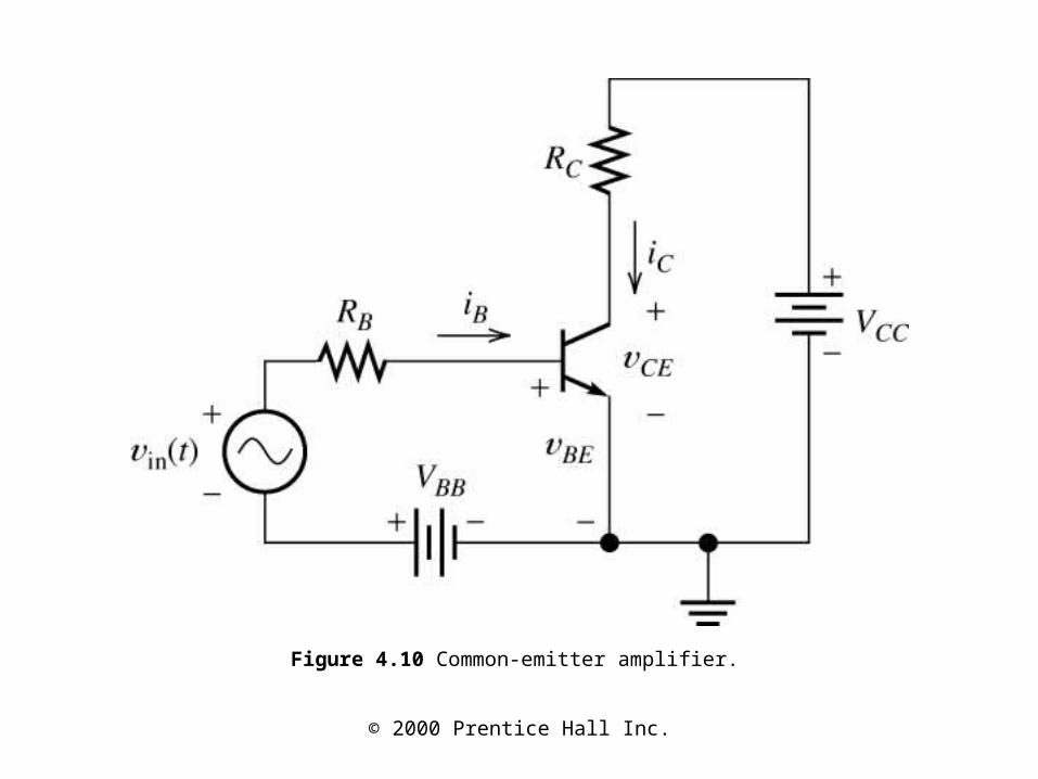
© 2000 Prentice Hall Inc.
Figure 4.10 Common-emitter amplifier.

© 2000 Prentice Hall Inc.
Figure 4.11 Load-line analysis of the amplifier of Figure 4.10.

© 2000 Prentice Hall Inc.
Figure 4.12a Load-line analysis for Example 4.2.

© 2000 Prentice Hall Inc.
Figure 4.12b Load-line analysis for Example 4.2.

© 2000 Prentice Hall Inc.
Figure 4.13 Voltage waveforms for the amplifier of Figure 4.10. See Example 4.2.

© 2000 Prentice Hall Inc.
Figure 4.14 Output of the amplifier of Example 4.2 for vin (t) = 1.2 sin(2000p t) showing gross distortion.

© 2000 Prentice Hall Inc.
Figure 4.15 Amplification occurs in the active region. Clipping occurs when the instantaneous operating point enters saturation or cutoff. In saturation, vCE < 0.2 V.

© 2000 Prentice Hall Inc.
Figure 4.16 The pnp BJT.

© 2000 Prentice Hall Inc.
Figure 4.17 Common-emitter characteristics for a pnp BJT.

© 2000 Prentice Hall Inc.
Figure 4.18 Common-emitter amplifier for Exercise 4.8.

© 2000 Prentice Hall Inc.
Figure 4.19a BJT large-signal models. (Note: Values shown are appropriate for typical small-signal silicon devices ata temperature of 300K.

© 2000 Prentice Hall Inc.
Figure 4.19b BJT large-signal models. (Note: Values shown are appropriate for typical small-signal silicon devices ata temperature of 300K.

© 2000 Prentice Hall Inc.
Figure 4.19c BJT large-signal models. (Note: Values shown are appropriate for typical small-signal silicon devices ata temperature of 300K.

© 2000 Prentice Hall Inc.
Figure 4.20 Regions of operation on the characteristics of an npn BJT.

© 2000 Prentice Hall Inc.
Figure 4.21 Bias circuit of Examples 4.4 and 4.5.

© 2000 Prentice Hall Inc.
Figure 4.22 Circuit for Example 4.4.

© 2000 Prentice Hall Inc.
Figure 4.25 Load lines for Examples 4.4 and 4.5.

© 2000 Prentice Hall Inc.
Figure 4.26 Circuit for Exercise 4.12.

© 2000 Prentice Hall Inc.
Figure 4.27 Circuit for Example 4.6.

© 2000 Prentice Hall Inc.
Figure 4.28a Four-resistor bias circuit.
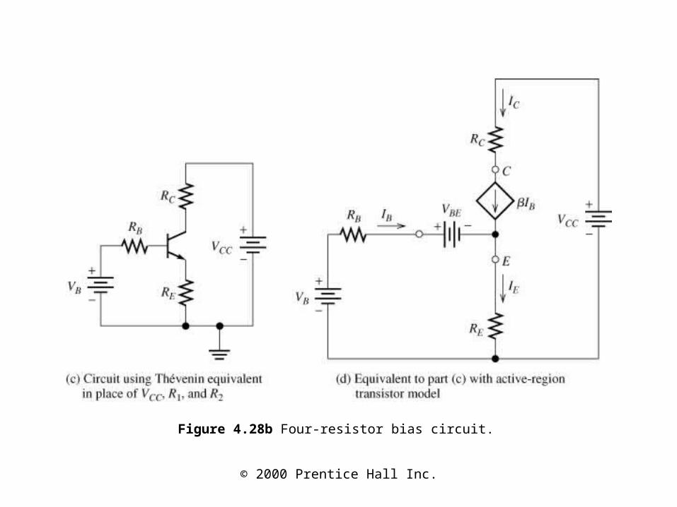
© 2000 Prentice Hall Inc.
Figure 4.28b Four-resistor bias circuit.
© 2000 Prentice Hall Inc.
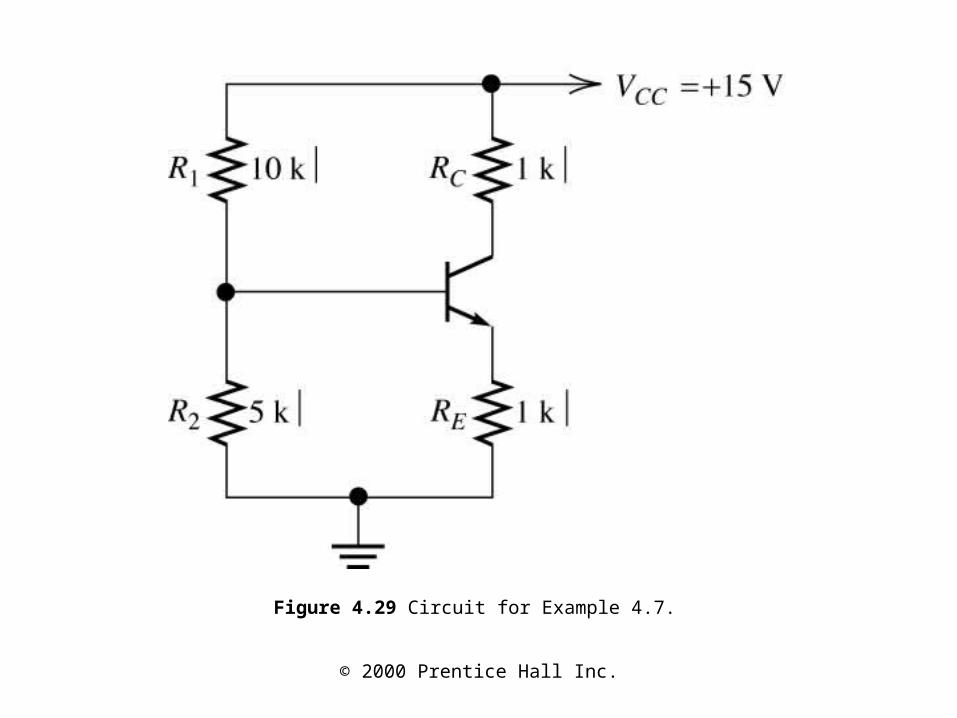
Figure 4.29 Circuit for Example 4.7.

© 2000 Prentice Hall Inc.
Figure 4.30 Current sources are useful in biasing IC amplifiers.

© 2000 Prentice Hall Inc.
Figure 4.31 Circuit for Exercise 4.18.

© 2000 Prentice Hall Inc.
Figure 4.32 Illustration of the Q-point base current IBQ, signal current i b(t), and total current iB(t).

© 2000 Prentice Hall Inc.
Figure 4.33 Small-signal equivalent circuits for the BJT.

© 2000 Prentice Hall Inc.
Figure 4.34a Common-emitter amplifier.

© 2000 Prentice Hall Inc.
Figure 4.34b Common-emitter amplifier.

© 2000 Prentice Hall Inc.
Figure 4.34c Common-emitter amplifier.

© 2000 Prentice Hall Inc.
Figure 4.35 Common-emitter amplifier of Example 4.9.

© 2000 Prentice Hall Inc.
Figure 4.36a Emitter follower.

© 2000 Prentice Hall Inc.
Figure 4.36b Emitter follower.

© 2000 Prentice Hall Inc.
Figure 4.36c Emitter follower.

© 2000 Prentice Hall Inc.
Figure 4.37a Emitter follower of Example 4.10.

© 2000 Prentice Hall Inc.
Figure 4.37b & c Emitter follower of Example 4.10.

© 2000 Prentice Hall Inc.
Figure 4.38 Common-base amplifier.

© 2000 Prentice Hall Inc.
Figure 4.39 Variation of the common-emitter amplifier.

© 2000 Prentice Hall Inc.
Figure 4.40 Small-signal equivalent circuit for the amplifier of Figure 4.39.

© 2000 Prentice Hall Inc.
Figure 4.41 RTL inverter.

© 2000 Prentice Hall Inc.
Figure 4.42a Load-line analysis of RTL inverter under no-load conditions.

© 2000 Prentice Hall Inc.
Figure 4.42b Load-line analysis of RTL inverter under no-load conditions.

© 2000 Prentice Hall Inc.
Figure 4.43 Transfer characteristic for RTL inverter under no-load conditions.

© 2000 Prentice Hall Inc.
Figure 4.44 Plots for Exercise 4.26.

© 2000 Prentice Hall Inc.
Figure 4.45 Three-input RTL NOR gate.

© 2000 Prentice Hall Inc.
Figure 4.46 RTL inverter.

© 2000 Prentice Hall Inc.
Figure 4.49 RTL inverter waveforms.

© 2000 Prentice Hall Inc.
Figure 4.50 Waveforms illustrating turn-on and turn-off times.

© 2000 Prentice Hall Inc.
Figure 4.51 The speed-up capacitor CS and Schottky clamp diode D1 dramatically reduce the switching times of the RTL inverter.

© 2000 Prentice Hall Inc.
Figure 4.53 Waveforms of the Schottky-clamped RTL inverter.