z. feng mtu ee4800 cmos digital ic design & analysis 2.1 ee4800 cmos digital ic design &...
TRANSCRIPT

Z. Feng MTU EE4800 CMOS Digital IC Design & AnalysisZ. Feng MTU EE4800 CMOS Digital IC Design & Analysis2.2.11
EE4800 CMOS Digital IC Design & Analysis
Lecture 2 CMOS Circuits and LayoutZhuo Feng

Z. Feng MTU EE4800 CMOS Digital IC Design & AnalysisZ. Feng MTU EE4800 CMOS Digital IC Design & Analysis2.2.22
Complementary CMOS■ Complementary CMOS logic gates
►NMOS pull-down network►PMOS pull-up network
pMOSpull-upnetwork
outputinputs
nMOSpull-downnetwork
Pull-up OFF Pull-up ON
Pull-down OFF Z (float) 1
Pull-down ON 0 X (shorted)
Z. Feng MTU EE4800 CMOS Digital IC Design & AnalysisZ. Feng MTU EE4800 CMOS Digital IC Design & Analysis2.2.33
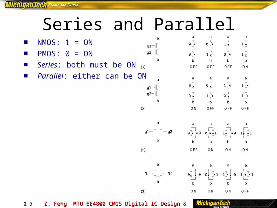
Series and Parallel■ NMOS: 1 = ON■ PMOS: 0 = ON■ Series: both must be ON■ Parallel: either can be ON
(a)
a
b
a
b
g1
g2
0
0
a
b
0
1
a
b
1
0
a
b
1
1
OFF OFF OFF ON
(b)
a
b
a
b
g1
g2
0
0
a
b
0
1
a
b
1
0
a
b
1
1
ON OFF OFF OFF
(c)
a
b
a
b
g1 g2 0 0
OFF ON ON ON
(d) ON ON ON OFF
a
b
0
a
b
1
a
b
11 0 1
a
b
0 0
a
b
0
a
b
1
a
b
11 0 1
a
b
g1 g2
Z. Feng MTU EE4800 CMOS Digital IC Design & AnalysisZ. Feng MTU EE4800 CMOS Digital IC Design & Analysis2.2.44
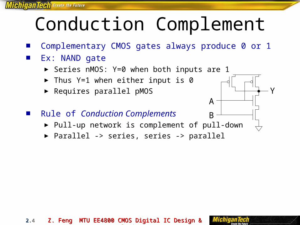
Conduction Complement■ Complementary CMOS gates always produce 0 or 1■ Ex: NAND gate
► Series nMOS: Y=0 when both inputs are 1► Thus Y=1 when either input is 0► Requires parallel pMOS
■ Rule of Conduction Complements► Pull-up network is complement of pull-down► Parallel -> series, series -> parallel
A
B
Y

Z. Feng MTU EE4800 CMOS Digital IC Design & AnalysisZ. Feng MTU EE4800 CMOS Digital IC Design & Analysis2.2.55
Compound Gates■ Compound gates can do any inverting
function■ Example:
(AND-AND-OR-INVERT, AOI22)Y A B C D
A
B
C
D
A
B
C
D
A B C DA B
C D
B
D
YA
CA
C
A
B
C
D
B
D
Y
(a)
(c)
(e)
(b)
(d)
(f)
Z. Feng MTU EE4800 CMOS Digital IC Design & AnalysisZ. Feng MTU EE4800 CMOS Digital IC Design & Analysis2.2.66
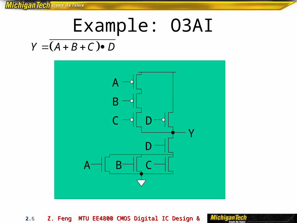
Example: O3AI
Y A B C D
A B
Y
C
D
DC
B
A
Z. Feng MTU EE4800 CMOS Digital IC Design & AnalysisZ. Feng MTU EE4800 CMOS Digital IC Design & Analysis2.2.77
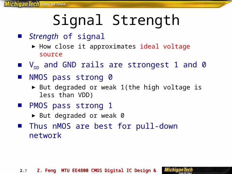
Signal Strength■ Strength of signal
► How close it approximates ideal voltage source
■ VDD and GND rails are strongest 1 and 0
■ NMOS pass strong 0► But degraded or weak 1(the high voltage is less than VDD)
■ PMOS pass strong 1► But degraded or weak 0
■ Thus nMOS are best for pull-down network

Z. Feng MTU EE4800 CMOS Digital IC Design & AnalysisZ. Feng MTU EE4800 CMOS Digital IC Design & Analysis2.2.88
Pass Transistors■ Transistors can be used as switches
► Pass transistor: NMOS or PMOS is used alone as an imperfect switch
g
s d
g = 0
s d
g = 1
s d
0 strong 0
Input Output
1 degraded 1
g
s d
g = 0
s d
g = 1
s d
0 degraded 0
Input Output
strong 1
g = 1
g = 1
g = 0
g = 0

Z. Feng MTU EE4800 CMOS Digital IC Design & AnalysisZ. Feng MTU EE4800 CMOS Digital IC Design & Analysis2.2.99
Transmission Gates■ Pass transistors produce degraded outputs■ Transmission gates pass both 0 and 1 well
g = 0, gb = 1
a b
g = 1, gb = 0
a b
0 strong 0
Input Output
1 strong 1
g
gb
a b
a b
g
gb
a b
g
gb
a b
g
gb
g = 1, gb = 0
g = 1, gb = 0
Z. Feng MTU EE4800 CMOS Digital IC Design & AnalysisZ. Feng MTU EE4800 CMOS Digital IC Design & Analysis2.2.1010
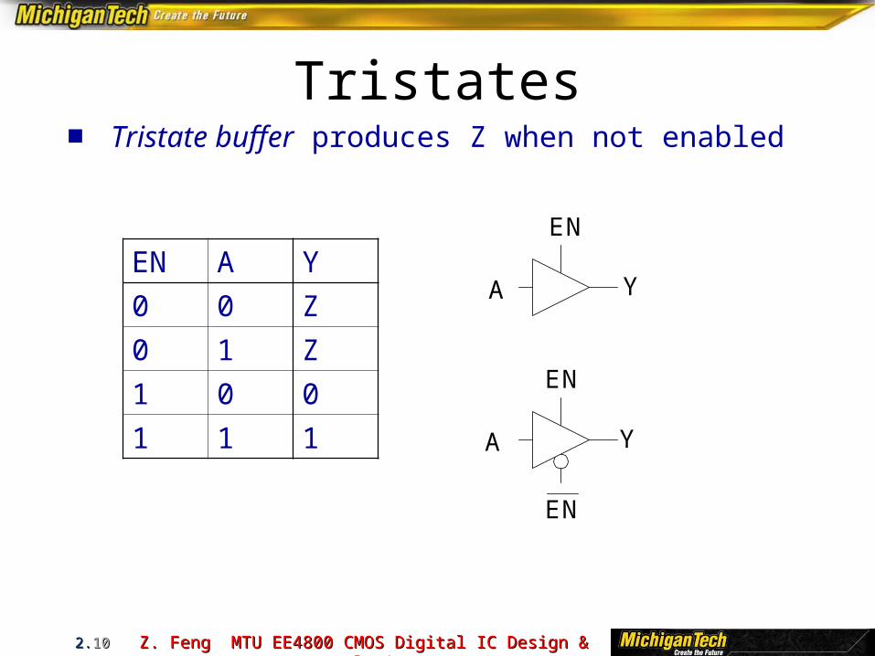
Tristates■ Tristate buffer produces Z when not enabled
EN A Y
0 0 Z
0 1 Z
1 0 0
1 1 1
A Y
EN
A Y
EN
EN
Z. Feng MTU EE4800 CMOS Digital IC Design & AnalysisZ. Feng MTU EE4800 CMOS Digital IC Design & Analysis2.2.1111
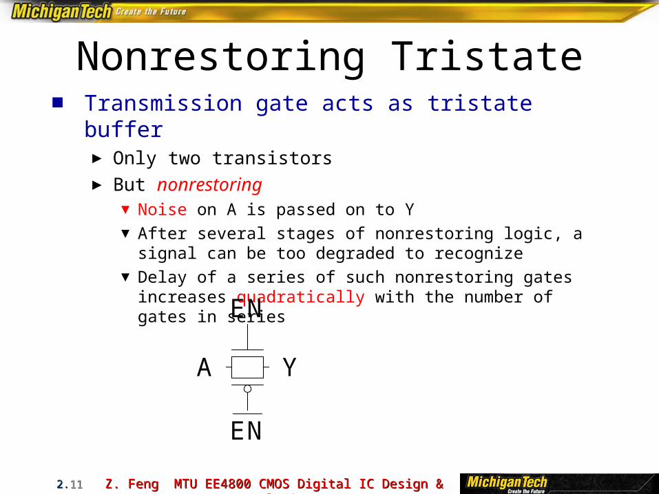
Nonrestoring Tristate■ Transmission gate acts as tristate buffer
► Only two transistors► But nonrestoring
▼ Noise on A is passed on to Y▼ After several stages of nonrestoring logic, a signal can be too
degraded to recognize▼ Delay of a series of such nonrestoring gates increases
quadratically with the number of gates in series
A Y
EN
EN
Z. Feng MTU EE4800 CMOS Digital IC Design & AnalysisZ. Feng MTU EE4800 CMOS Digital IC Design & Analysis2.2.1212
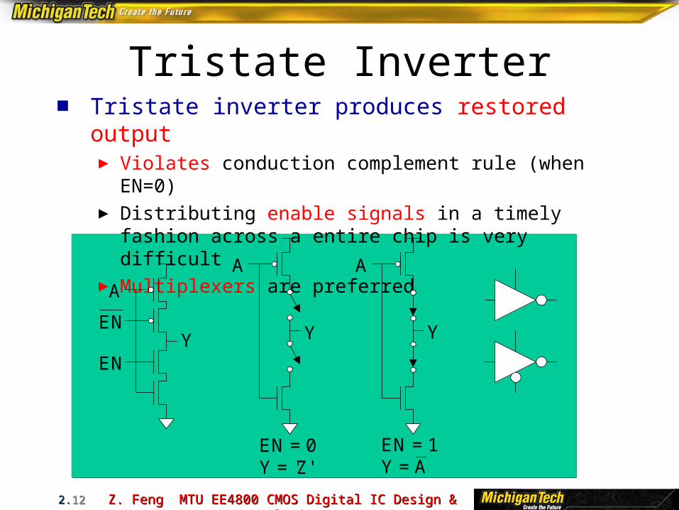
Tristate Inverter■ Tristate inverter produces restored output
► Violates conduction complement rule (when EN=0)► Distributing enable signals in a timely fashion across a
entire chip is very difficult► Multiplexers are preferred
A
YEN
A
Y
EN = 0Y = 'Z'
Y
EN = 1Y = A
A
EN
Z. Feng MTU EE4800 CMOS Digital IC Design & AnalysisZ. Feng MTU EE4800 CMOS Digital IC Design & Analysis2.2.1313
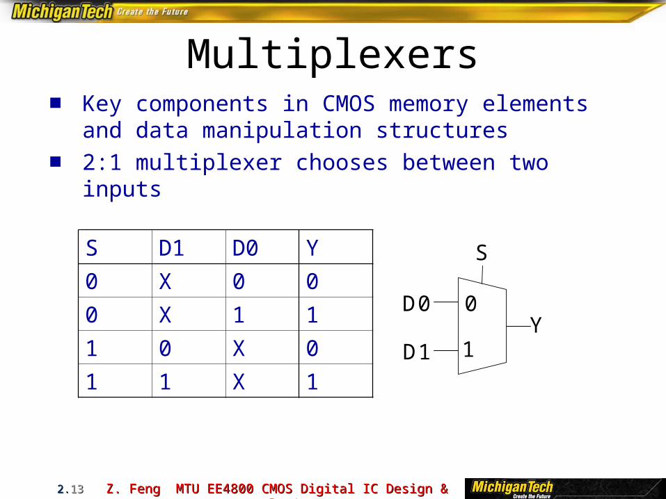
Multiplexers■ Key components in CMOS memory elements
and data manipulation structures■ 2:1 multiplexer chooses between two inputs
S D1 D0 Y
0 X 0 0
0 X 1 1
1 0 X 0
1 1 X 1
0
1
S
D0
D1Y
Z. Feng MTU EE4800 CMOS Digital IC Design & AnalysisZ. Feng MTU EE4800 CMOS Digital IC Design & Analysis2.2.1414
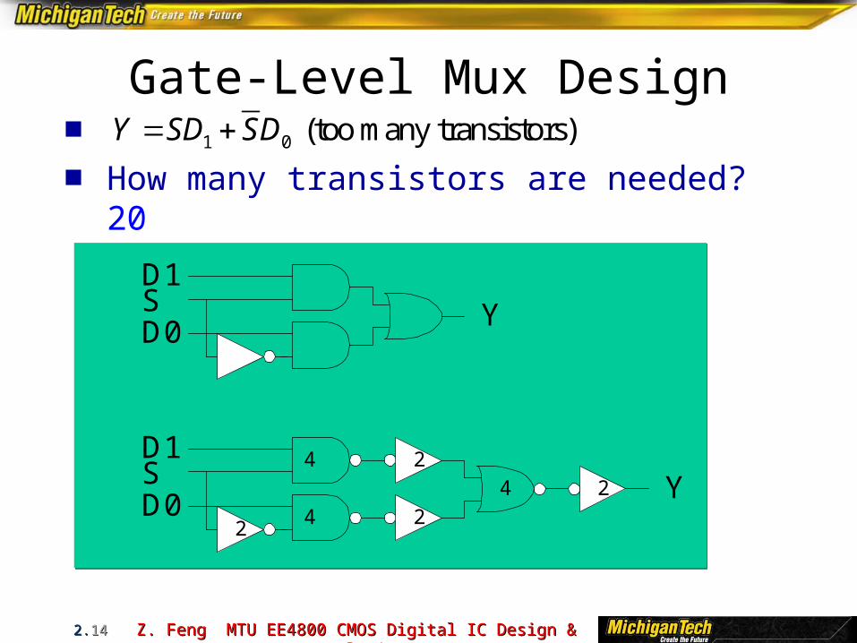
Gate-Level Mux Design■ ■ How many transistors are needed? 20
1 0 (too many transistors)Y SD SD
44
D1
D0S Y
4
2
2
2 Y2
D1
D0S

Z. Feng MTU EE4800 CMOS Digital IC Design & AnalysisZ. Feng MTU EE4800 CMOS Digital IC Design & Analysis2.2.1515
Transmission Gate Mux■ Nonrestoring mux uses two transmission
gates► Only 4 transistors
S
S
D0
D1
YS

Z. Feng MTU EE4800 CMOS Digital IC Design & AnalysisZ. Feng MTU EE4800 CMOS Digital IC Design & Analysis2.2.1616
Inverting Mux■ Inverting multiplexer
► Use compound AOI22► Or pair of tristate inverters► Essentially the same thing
■ Noninverting multiplexer adds an inverter
S
D0 D1
Y
S
D0
D1Y
0
1S
Y
D0
D1
S
S
S
S
S
S

Z. Feng MTU EE4800 CMOS Digital IC Design & AnalysisZ. Feng MTU EE4800 CMOS Digital IC Design & Analysis2.2.1717
4:1 Multiplexer■ 4:1 mux chooses one of 4 inputs using two
selects► Two levels of 2:1 muxes► Or four tristates
S0
D0
D1
0
1
0
1
0
1Y
S1
D2
D3
D0
D1
D2
D3
Y
S1S0 S1S0 S1S0 S1S0

Z. Feng MTU EE4800 CMOS Digital IC Design & AnalysisZ. Feng MTU EE4800 CMOS Digital IC Design & Analysis2.2.1818
D Latch■ When CLK = 1, latch is transparent
► D flows through to Q like a buffer
■ When CLK = 0, the latch is opaque► Q holds its old value independent of D
■ a.k.a. transparent latch or level-sensitive latch
CLK
D Q
Latc
h D
CLK
Q
Z. Feng MTU EE4800 CMOS Digital IC Design & AnalysisZ. Feng MTU EE4800 CMOS Digital IC Design & Analysis2.2.1919
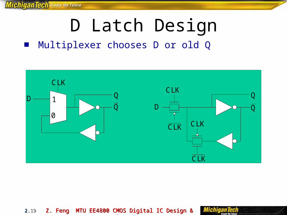
D Latch Design■ Multiplexer chooses D or old Q
1
0
D
CLK
QCLK
CLKCLK
CLK
DQ Q
Q
Z. Feng MTU EE4800 CMOS Digital IC Design & AnalysisZ. Feng MTU EE4800 CMOS Digital IC Design & Analysis2.2.2020
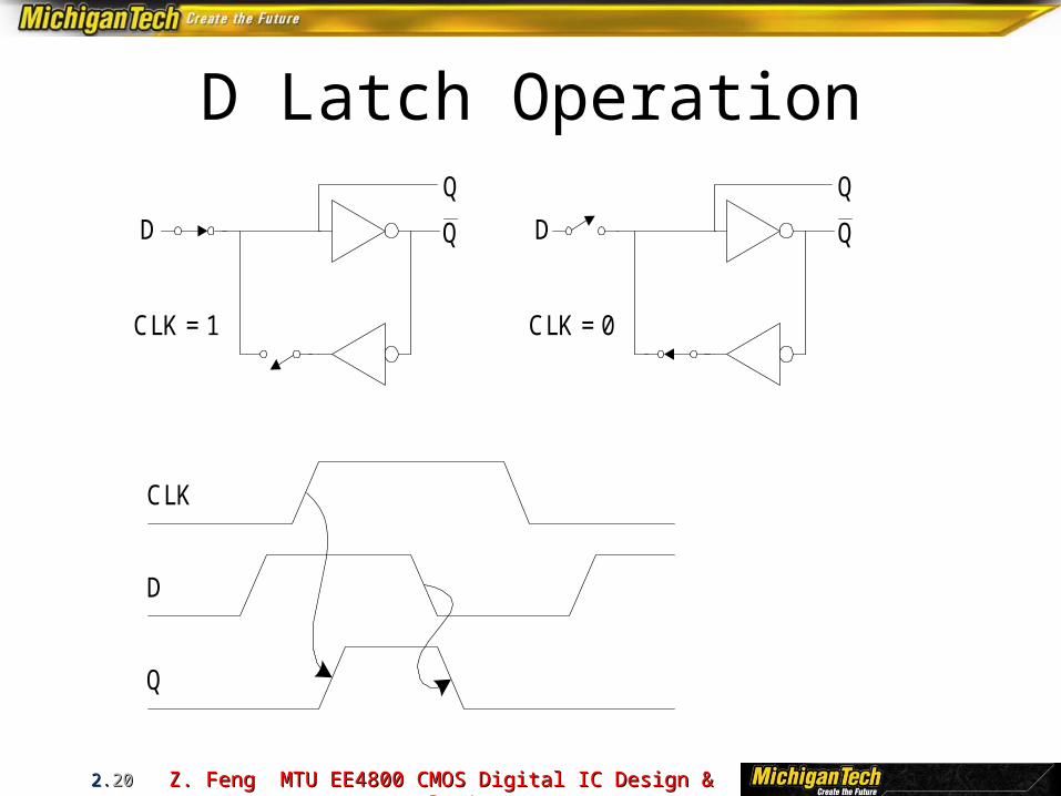
D Latch Operation
CLK = 1
D Q
Q
CLK = 0
D Q
Q
D
CLK
Q

Z. Feng MTU EE4800 CMOS Digital IC Design & AnalysisZ. Feng MTU EE4800 CMOS Digital IC Design & Analysis2.2.2121
D Flip-flop■ When CLK rises, D is copied to Q■ At all other times, Q holds its value■ a.k.a. positive edge-triggered flip-flop, master-slave
flip-flop■ Collection of two or more D flip-flops sharing a common
clock input is called a register (multi-bit)
Flo
p
CLK
D QD
CLK
Q
Z. Feng MTU EE4800 CMOS Digital IC Design & AnalysisZ. Feng MTU EE4800 CMOS Digital IC Design & Analysis2.2.2222
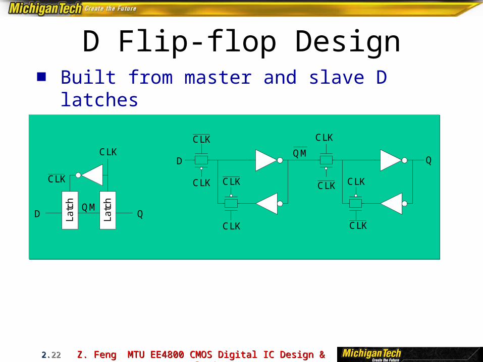
D Flip-flop Design■ Built from master and slave D latches
QM
CLK
CLKCLK
CLK
Q
CLK
CLK
CLK
CLK
D
Latc
h
Latc
h
D QQM
CLK
CLK

Z. Feng MTU EE4800 CMOS Digital IC Design & AnalysisZ. Feng MTU EE4800 CMOS Digital IC Design & Analysis2.2.2323
D Flip-flop Operation
CLK = 1
D
CLK = 0
Q
D
QM
QMQ
D
CLK
Q

Z. Feng MTU EE4800 CMOS Digital IC Design & AnalysisZ. Feng MTU EE4800 CMOS Digital IC Design & Analysis2.2.2424
Race Condition■ Back-to-back flops can malfunction from clock
skew► Second flip-flop fires late► Sees first flip-flop change and captures its result► Called hold-time failure or race condition
CLK1
D Q1
Flo
p
Flo
p
CLK2
Q2
CLK1
CLK2
Q1
Q2

Z. Feng MTU EE4800 CMOS Digital IC Design & AnalysisZ. Feng MTU EE4800 CMOS Digital IC Design & Analysis2.2.2525
Nonoverlapping Clocks■ Nonoverlapping clocks can prevent races
► As long as nonoverlap exceeds clock skew► Industry manages skew more carefully
1
11
1
2
22
2
2
1
QMQD
Z. Feng MTU EE4800 CMOS Digital IC Design & AnalysisZ. Feng MTU EE4800 CMOS Digital IC Design & Analysis2.2.2626
Layout■ Chips are specified with set of masks■ Minimum dimensions of masks determine
transistor size (and hence speed, cost, and power)
■ Feature size f = distance between source and drain
► Set by minimum width of polysilicon
■ Feature size improves 30% every 3 years or so
■ Normalize for feature size when describing design rules
■ Express rules in terms of = f/2► E.g. = 0.3 m in 0.6 m process
Z. Feng MTU EE4800 CMOS Digital IC Design & AnalysisZ. Feng MTU EE4800 CMOS Digital IC Design & Analysis2.2.2727
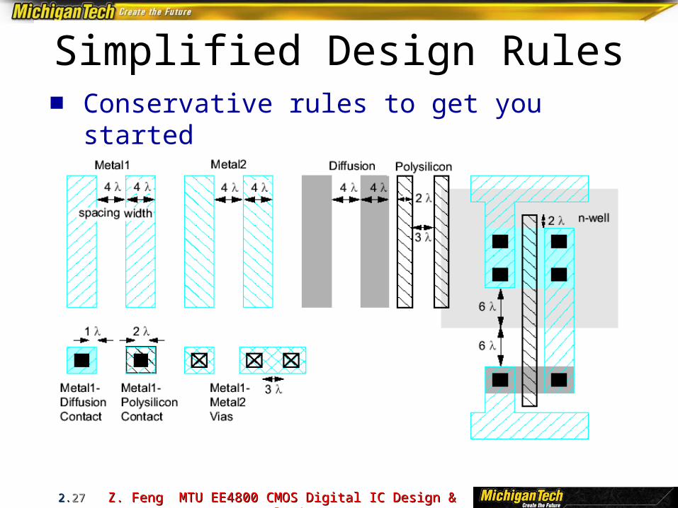
Simplified Design Rules■ Conservative rules to get you started

Z. Feng MTU EE4800 CMOS Digital IC Design & AnalysisZ. Feng MTU EE4800 CMOS Digital IC Design & Analysis2.2.2828
Inverter Layout■ Transistor dimensions specified as Width /
Length► Minimum size is 4 / 2sometimes called 1 unit► In f = 0.6 m process, this is 1.2 m wide, 0.6 m long

Z. Feng MTU EE4800 CMOS Digital IC Design & AnalysisZ. Feng MTU EE4800 CMOS Digital IC Design & Analysis2.2.2929
Gate Layout■ Layout can be very time consuming
► Design gates to fit together nicely► Build a library of standard cells
■ Standard cell design methodology► VDD and GND should abut (standard height)
► Adjacent gates should satisfy design rules► nMOS at bottom and pMOS at top► All gates include well and substrate contacts
Z. Feng MTU EE4800 CMOS Digital IC Design & AnalysisZ. Feng MTU EE4800 CMOS Digital IC Design & Analysis2.2.3030
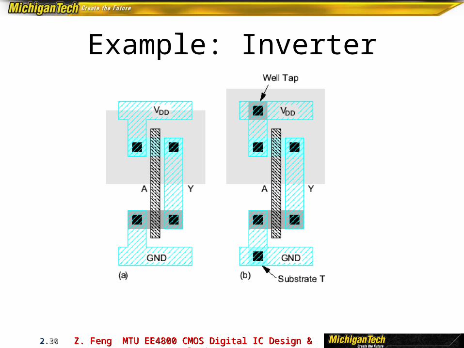
Example: Inverter

Z. Feng MTU EE4800 CMOS Digital IC Design & AnalysisZ. Feng MTU EE4800 CMOS Digital IC Design & Analysis2.2.3131
Example: NAND3■ Horizontal N-diffusion and P-diffusion strips■ Vertical polysilicon gates
■ Metal1 VDD rail at top
■ Metal1 GND rail at bottom■ 32 by 40
Z. Feng MTU EE4800 CMOS Digital IC Design & AnalysisZ. Feng MTU EE4800 CMOS Digital IC Design & Analysis2.2.3232
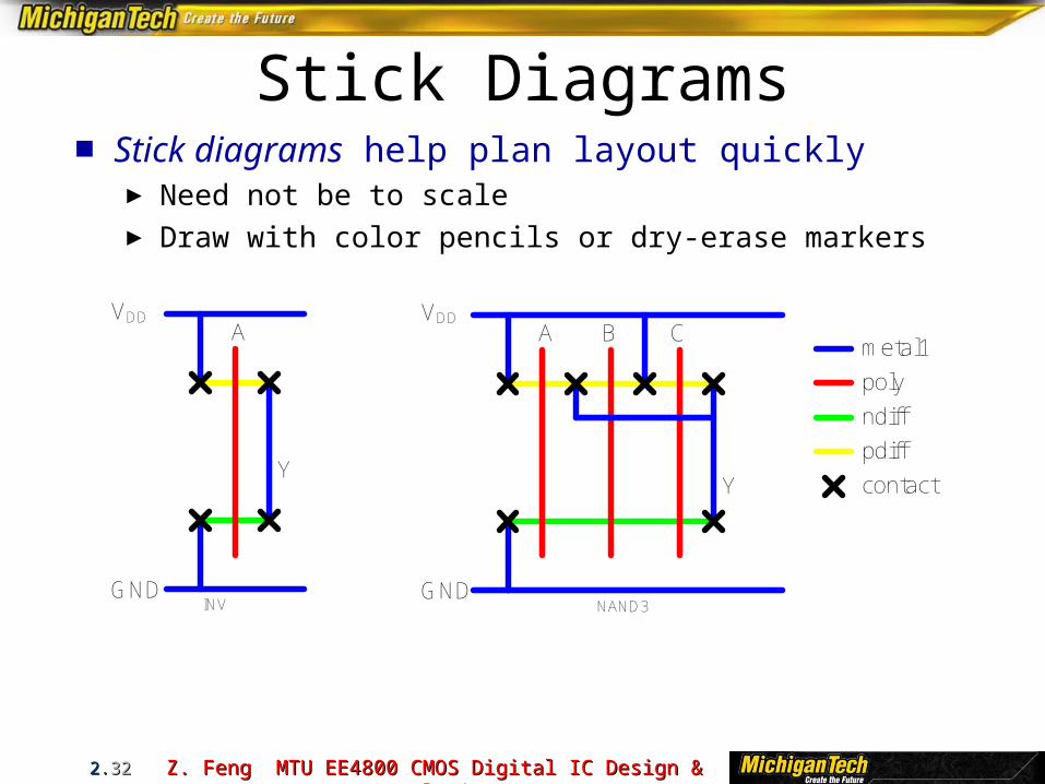
Stick Diagrams■ Stick diagrams help plan layout quickly
► Need not be to scale► Draw with color pencils or dry-erase markers
c
AVDD
GND
Y
AVDD
GND
B C
Y
INV
metal1
poly
ndiff
pdiff
contact
NAND3

Z. Feng MTU EE4800 CMOS Digital IC Design & AnalysisZ. Feng MTU EE4800 CMOS Digital IC Design & Analysis2.2.3333
Wiring Tracks■ A wiring track is the space required for a wire
► 4 width, 4 spacing from neighbor = 8 pitch
■ Transistors also consume one wiring track

Z. Feng MTU EE4800 CMOS Digital IC Design & AnalysisZ. Feng MTU EE4800 CMOS Digital IC Design & Analysis2.2.3434
Well spacing■ Wells must surround transistors by 6
► Implies 12 between opposite transistor flavors► Leaves room for one wire track

Z. Feng MTU EE4800 CMOS Digital IC Design & AnalysisZ. Feng MTU EE4800 CMOS Digital IC Design & Analysis2.2.3535
32
40
Area Estimation■ Estimate area by counting wiring tracks
► Multiply by 8 to express in
Z. Feng MTU EE4800 CMOS Digital IC Design & AnalysisZ. Feng MTU EE4800 CMOS Digital IC Design & Analysis2.2.3636
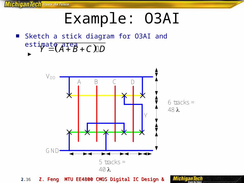
Example: O3AI■ Sketch a stick diagram for O3AI and estimate
area►
Y A B C D
AVDD
GND
B C
Y
D
6 tracks = 48
5 tracks = 40