xilinx cpld libraries guide · 2019-10-13 · cb16cled.....103 cb16re.....105
TRANSCRIPT

CPLD Libraries GuideISE 10.1

Xilinx Trademarks and Copyright Information
Xilinx is disclosing this user guide, manual, release note, and/or specification (the “Documentation”) to yousolely for use in the development of designs to operate with Xilinx hardware devices. You may not reproduce,distribute, republish, download, display, post, or transmit the Documentation in any form or by any meansincluding, but not limited to, electronic, mechanical, photocopying, recording, or otherwise, without the priorwritten consent of Xilinx. Xilinx expressly disclaims any liability arising out of your use of the Documentation.Xilinx reserves the right, at its sole discretion, to change the Documentation without notice at any time. Xilinxassumes no obligation to correct any errors contained in the Documentation, or to advise you of any correctionsor updates. Xilinx expressly disclaims any liability in connection with technical support or assistance that may beprovided to you in connection with the Information.
THE DOCUMENTATION IS DISCLOSED TO YOU “AS-IS” WITH NOWARRANTY OF ANY KIND. XILINXMAKES NO OTHER WARRANTIES, WHETHER EXPRESS, IMPLIED, OR STATUTORY, REGARDINGTHE DOCUMENTATION, INCLUDING ANY WARRANTIES OF MERCHANTABILITY, FITNESS FOR APARTICULAR PURPOSE, OR NONINFRINGEMENT OF THIRD-PARTY RIGHTS. IN NO EVENT WILLXILINX BE LIABLE FOR ANY CONSEQUENTIAL, INDIRECT, EXEMPLARY, SPECIAL, OR INCIDENTALDAMAGES, INCLUDING ANY LOSS OF DATA OR LOST PROFITS, ARISING FROM YOUR USE OF THEDOCUMENTATION.
© Copyright 2002 – 2008 Xilinx, Inc. All Rights Reserved. XILINX, the Xilinx logo, the Brand Window and otherdesignated brands included herein are trademarks of Xilinx, Inc. All other trademarks are the property oftheir respective owners.
Libraries Guide
2 www.xilinx.com 10.1

Table of ContentsAbout this Guide ........................................................................................................................................ 11Functional Categories ................................................................................................................................. 13About Design Elements............................................................................................................................... 29
ACC1.................................................................................................................................................. 30ACC16 ................................................................................................................................................ 32ACC4.................................................................................................................................................. 34ACC8.................................................................................................................................................. 37ADD1 ................................................................................................................................................. 39ADD16................................................................................................................................................ 40ADD4 ................................................................................................................................................. 42ADD8 ................................................................................................................................................. 44ADSU1................................................................................................................................................ 46ADSU16 .............................................................................................................................................. 48ADSU4................................................................................................................................................ 50ADSU8................................................................................................................................................ 52AND2 ................................................................................................................................................. 54AND2B1.............................................................................................................................................. 55AND2B2.............................................................................................................................................. 56AND3 ................................................................................................................................................. 57AND3B1.............................................................................................................................................. 58AND3B2.............................................................................................................................................. 59AND3B3.............................................................................................................................................. 60AND4 ................................................................................................................................................. 61AND4B1.............................................................................................................................................. 62AND4B2.............................................................................................................................................. 63AND4B3.............................................................................................................................................. 64AND4B4.............................................................................................................................................. 65AND5 ................................................................................................................................................. 66AND5B1.............................................................................................................................................. 67AND5B2.............................................................................................................................................. 68AND5B3.............................................................................................................................................. 69AND5B4.............................................................................................................................................. 70AND5B5.............................................................................................................................................. 71AND6 ................................................................................................................................................. 72AND7 ................................................................................................................................................. 73AND8 ................................................................................................................................................. 74AND9 ................................................................................................................................................. 75BRLSHFT4 .......................................................................................................................................... 76BRLSHFT8 .......................................................................................................................................... 77BUF .................................................................................................................................................... 79BUF16 ................................................................................................................................................. 80BUF4................................................................................................................................................... 81BUF8................................................................................................................................................... 82BUFE .................................................................................................................................................. 83BUFE16 ............................................................................................................................................... 84BUFE4................................................................................................................................................. 85BUFE8................................................................................................................................................. 87BUFG.................................................................................................................................................. 88BUFGSR.............................................................................................................................................. 90BUFGTS .............................................................................................................................................. 91BUFT .................................................................................................................................................. 92BUFT16 ............................................................................................................................................... 93BUFT4................................................................................................................................................. 95BUFT8................................................................................................................................................. 97CB16CE............................................................................................................................................... 99CB16CLE............................................................................................................................................ 101
Libraries Guide
10.1 www.xilinx.com 3

CB16CLED ......................................................................................................................................... 103CB16RE.............................................................................................................................................. 105CB16RLE............................................................................................................................................ 107CB16X1 .............................................................................................................................................. 109CB16X2 .............................................................................................................................................. 111CB2CE ............................................................................................................................................... 113CB2CLE ............................................................................................................................................. 115CB2CLED........................................................................................................................................... 117CB2RE................................................................................................................................................ 119CB2RLE ............................................................................................................................................. 121CB2X1................................................................................................................................................ 123CB2X2................................................................................................................................................ 125CB4CE ............................................................................................................................................... 127CB4CLE ............................................................................................................................................. 129CB4CLED........................................................................................................................................... 131CB4RE................................................................................................................................................ 133CB4RLE ............................................................................................................................................. 135CB4X1................................................................................................................................................ 137CB4X2................................................................................................................................................ 139CB8CE ............................................................................................................................................... 141CB8CLE ............................................................................................................................................. 143CB8CLED........................................................................................................................................... 145CB8RE................................................................................................................................................ 147CB8RLE ............................................................................................................................................. 149CB8X1................................................................................................................................................ 151CB8X2................................................................................................................................................ 153CBD16CE ........................................................................................................................................... 155CBD16CLE ......................................................................................................................................... 157CBD16CLED....................................................................................................................................... 159CBD16RE ........................................................................................................................................... 161CBD16RLE ......................................................................................................................................... 163CBD16X1............................................................................................................................................ 165CBD16X2............................................................................................................................................ 167CBD2CE............................................................................................................................................. 169CBD2CLE........................................................................................................................................... 171CBD2CLED ........................................................................................................................................ 173CBD2RE............................................................................................................................................. 175CBD2RLE........................................................................................................................................... 177CBD2X1 ............................................................................................................................................. 179CBD2X2 ............................................................................................................................................. 181CBD4CE............................................................................................................................................. 183CBD4CLE........................................................................................................................................... 185CBD4CLED ........................................................................................................................................ 187CBD4RE............................................................................................................................................. 189CBD4RLE........................................................................................................................................... 191CBD4X1 ............................................................................................................................................. 193CBD4X2 ............................................................................................................................................. 195CBD8CE............................................................................................................................................. 197CBD8CLE........................................................................................................................................... 199CBD8CLED ........................................................................................................................................ 201CBD8RE............................................................................................................................................. 203CBD8RLE........................................................................................................................................... 205CBD8X1 ............................................................................................................................................. 207CBD8X2 ............................................................................................................................................. 209CD4CE............................................................................................................................................... 211CD4CLE............................................................................................................................................. 213CD4RE ............................................................................................................................................... 215CD4RLE............................................................................................................................................. 217CDD4CE ............................................................................................................................................ 219
Libraries Guide
4 www.xilinx.com 10.1

CDD4CLE .......................................................................................................................................... 221CDD4RE ............................................................................................................................................ 223CDD4RLE .......................................................................................................................................... 225CJ4CE ................................................................................................................................................ 226CJ4RE ................................................................................................................................................ 227CJ5CE ................................................................................................................................................ 228CJ5RE ................................................................................................................................................ 230CJ8CE ................................................................................................................................................ 232CJ8RE ................................................................................................................................................ 233CJD4CE.............................................................................................................................................. 234CJD4RE.............................................................................................................................................. 235CJD5CE.............................................................................................................................................. 237CJD5RE.............................................................................................................................................. 239CJD8CE.............................................................................................................................................. 241CJD8RE.............................................................................................................................................. 242CLK_DIV10 ........................................................................................................................................ 244CLK_DIV10R...................................................................................................................................... 246CLK_DIV10RSD ................................................................................................................................. 248CLK_DIV10SD.................................................................................................................................... 250CLK_DIV12 ........................................................................................................................................ 252CLK_DIV12R...................................................................................................................................... 254CLK_DIV12RSD ................................................................................................................................. 256CLK_DIV12SD.................................................................................................................................... 258CLK_DIV14 ........................................................................................................................................ 260CLK_DIV14R...................................................................................................................................... 262CLK_DIV14RSD ................................................................................................................................. 264CLK_DIV14SD.................................................................................................................................... 266CLK_DIV16 ........................................................................................................................................ 268CLK_DIV16R...................................................................................................................................... 270CLK_DIV16RSD ................................................................................................................................. 272CLK_DIV16SD.................................................................................................................................... 274CLK_DIV2.......................................................................................................................................... 276CLK_DIV2R ....................................................................................................................................... 278CLK_DIV2RSD ................................................................................................................................... 280CLK_DIV2SD ..................................................................................................................................... 282CLK_DIV4.......................................................................................................................................... 284CLK_DIV4R ....................................................................................................................................... 286CLK_DIV4RSD ................................................................................................................................... 288CLK_DIV4SD ..................................................................................................................................... 290CLK_DIV6.......................................................................................................................................... 292CLK_DIV6R ....................................................................................................................................... 294CLK_DIV6RSD ................................................................................................................................... 296CLK_DIV6SD ..................................................................................................................................... 298CLK_DIV8.......................................................................................................................................... 300CLK_DIV8R ....................................................................................................................................... 302CLK_DIV8RSD ................................................................................................................................... 304CLK_DIV8SD ..................................................................................................................................... 306COMP16 ............................................................................................................................................ 308COMP2 .............................................................................................................................................. 309COMP4 .............................................................................................................................................. 310COMP8 .............................................................................................................................................. 311COMPM16 ......................................................................................................................................... 312COMPM2........................................................................................................................................... 314COMPM4........................................................................................................................................... 316COMPM8........................................................................................................................................... 318CR16CE.............................................................................................................................................. 320CR8CE ............................................................................................................................................... 321CRD16CE........................................................................................................................................... 322CRD8CE............................................................................................................................................. 324
Libraries Guide
10.1 www.xilinx.com 5
D2_4E ................................................................................................................................................ 326D3_8E ................................................................................................................................................ 327D4_16E............................................................................................................................................... 329FD ..................................................................................................................................................... 330FD16 .................................................................................................................................................. 331FD16CE.............................................................................................................................................. 332FD16RE.............................................................................................................................................. 334FD4.................................................................................................................................................... 336FD4CE ............................................................................................................................................... 337FD4RE ............................................................................................................................................... 339FD8.................................................................................................................................................... 341FD8CE ............................................................................................................................................... 342FD8RE ............................................................................................................................................... 344FDC ................................................................................................................................................... 346FDCE ................................................................................................................................................. 347FDCP ................................................................................................................................................. 349FDCPE ............................................................................................................................................... 351FDD................................................................................................................................................... 354FDD16 ............................................................................................................................................... 355FDD16CE ........................................................................................................................................... 356FDD16RE ........................................................................................................................................... 357FDD4 ................................................................................................................................................. 358FDD4CE............................................................................................................................................. 359FDD4RE............................................................................................................................................. 361FDD8 ................................................................................................................................................. 363FDD8CE............................................................................................................................................. 364FDD8RE............................................................................................................................................. 365FDDC ................................................................................................................................................ 366FDDCE .............................................................................................................................................. 367FDDCP .............................................................................................................................................. 369FDDCPE ............................................................................................................................................ 371FDDP................................................................................................................................................. 373FDDPE............................................................................................................................................... 374FDDR................................................................................................................................................. 376FDDRE............................................................................................................................................... 377FDDRS............................................................................................................................................... 378FDDRSE............................................................................................................................................. 380FDDS ................................................................................................................................................. 382FDDSE ............................................................................................................................................... 384FDDSR............................................................................................................................................... 386FDDSRE............................................................................................................................................. 388FDP ................................................................................................................................................... 390FDPE ................................................................................................................................................. 392FDR ................................................................................................................................................... 394FDRE ................................................................................................................................................. 396FDRS ................................................................................................................................................. 398FDRSE ............................................................................................................................................... 401FDS.................................................................................................................................................... 404FDSE.................................................................................................................................................. 406FDSR ................................................................................................................................................. 408FDSRE ............................................................................................................................................... 410FJKC .................................................................................................................................................. 412FJKCE ................................................................................................................................................ 414FJKCP ................................................................................................................................................ 416FJKCPE .............................................................................................................................................. 418FJKP .................................................................................................................................................. 420FJKPE ................................................................................................................................................ 422FJKRSE .............................................................................................................................................. 424FJKSRE .............................................................................................................................................. 426
Libraries Guide
6 www.xilinx.com 10.1

FTC.................................................................................................................................................... 428FTCE.................................................................................................................................................. 429FTCLE ............................................................................................................................................... 430FTCLEX ............................................................................................................................................. 432FTCP.................................................................................................................................................. 434FTCPE................................................................................................................................................ 436FTCPLE ............................................................................................................................................. 437FTDCE ............................................................................................................................................... 439FTDCLE............................................................................................................................................. 440FTDCLEX........................................................................................................................................... 442FTDCP ............................................................................................................................................... 444FTDRSE ............................................................................................................................................. 446FTDRSLE ........................................................................................................................................... 448FTP .................................................................................................................................................... 450FTPE.................................................................................................................................................. 451FTPLE................................................................................................................................................ 452FTRSE ................................................................................................................................................ 454FTRSLE.............................................................................................................................................. 456FTSRE................................................................................................................................................ 458FTSRLE.............................................................................................................................................. 460GND.................................................................................................................................................. 462IBUF .................................................................................................................................................. 463IBUF16 ............................................................................................................................................... 466IBUF4................................................................................................................................................. 467IBUF8................................................................................................................................................. 469INV.................................................................................................................................................... 470INV16 ................................................................................................................................................ 471INV4.................................................................................................................................................. 472INV8.................................................................................................................................................. 473IOBUFE.............................................................................................................................................. 474KEEPER ............................................................................................................................................. 476LD ..................................................................................................................................................... 478LD16.................................................................................................................................................. 479LD4.................................................................................................................................................... 481LD8.................................................................................................................................................... 483LDC................................................................................................................................................... 485LDCP................................................................................................................................................. 487LDG................................................................................................................................................... 489LDG16 ............................................................................................................................................... 490LDG4 ................................................................................................................................................. 492LDG8 ................................................................................................................................................. 494LDP ................................................................................................................................................... 496M16_1E .............................................................................................................................................. 498M2_1.................................................................................................................................................. 500M2_1B1 .............................................................................................................................................. 501M2_1B2 .............................................................................................................................................. 502M2_1E................................................................................................................................................ 503M4_1E................................................................................................................................................ 504M8_1E................................................................................................................................................ 505NAND2 ............................................................................................................................................. 507NAND2B1.......................................................................................................................................... 508NAND2B2.......................................................................................................................................... 509NAND3 ............................................................................................................................................. 510NAND3B1.......................................................................................................................................... 511NAND3B2.......................................................................................................................................... 512NAND3B3.......................................................................................................................................... 513NAND4 ............................................................................................................................................. 514NAND4B1.......................................................................................................................................... 515NAND4B2.......................................................................................................................................... 516
Libraries Guide
10.1 www.xilinx.com 7

NAND4B3.......................................................................................................................................... 517NAND4B4.......................................................................................................................................... 518NAND5 ............................................................................................................................................. 519NAND5B1.......................................................................................................................................... 520NAND5B2.......................................................................................................................................... 521NAND5B3.......................................................................................................................................... 522NAND5B4.......................................................................................................................................... 523NAND5B5.......................................................................................................................................... 524NAND6 ............................................................................................................................................. 525NAND7 ............................................................................................................................................. 526NAND8 ............................................................................................................................................. 527NAND9 ............................................................................................................................................. 528NOR2................................................................................................................................................. 529NOR2B1............................................................................................................................................. 530NOR2B2............................................................................................................................................. 531NOR3................................................................................................................................................. 532NOR3B1............................................................................................................................................. 533NOR3B2............................................................................................................................................. 534NOR3B3............................................................................................................................................. 535NOR4................................................................................................................................................. 536NOR4B1............................................................................................................................................. 537NOR4B2............................................................................................................................................. 538NOR4B3............................................................................................................................................. 539NOR4B4............................................................................................................................................. 540NOR5................................................................................................................................................. 541NOR5B1............................................................................................................................................. 542NOR5B2............................................................................................................................................. 543NOR5B3............................................................................................................................................. 544NOR5B4............................................................................................................................................. 545NOR5B5............................................................................................................................................. 546NOR6................................................................................................................................................. 547NOR7................................................................................................................................................. 548NOR8................................................................................................................................................. 549NOR9................................................................................................................................................. 550OBUF................................................................................................................................................. 551OBUF16 ............................................................................................................................................. 553OBUF4 ............................................................................................................................................... 554OBUF8 ............................................................................................................................................... 555OBUFE............................................................................................................................................... 556OBUFE16 ........................................................................................................................................... 557OBUFE4 ............................................................................................................................................. 558OBUFE8 ............................................................................................................................................. 559OBUFT............................................................................................................................................... 560OBUFT16 ........................................................................................................................................... 562OBUFT4 ............................................................................................................................................. 564OBUFT8 ............................................................................................................................................. 566OR2 ................................................................................................................................................... 568OR2B1................................................................................................................................................ 569OR2B2................................................................................................................................................ 570OR3 ................................................................................................................................................... 571OR3B1................................................................................................................................................ 572OR3B2................................................................................................................................................ 573OR3B3................................................................................................................................................ 574OR4 ................................................................................................................................................... 575OR4B1................................................................................................................................................ 576OR4B2................................................................................................................................................ 577OR4B3................................................................................................................................................ 578OR4B4................................................................................................................................................ 579OR5 ................................................................................................................................................... 580
Libraries Guide
8 www.xilinx.com 10.1
OR5B1................................................................................................................................................ 581OR5B2................................................................................................................................................ 582OR5B3................................................................................................................................................ 583OR5B4................................................................................................................................................ 584OR5B5................................................................................................................................................ 585OR6 ................................................................................................................................................... 586OR7 ................................................................................................................................................... 587OR8 ................................................................................................................................................... 588OR9 ................................................................................................................................................... 589PULLDOWN...................................................................................................................................... 590PULLUP............................................................................................................................................. 592SR16CE .............................................................................................................................................. 594SR16CLE ............................................................................................................................................ 596SR16CLED.......................................................................................................................................... 598SR16RE .............................................................................................................................................. 600SR16RLE ............................................................................................................................................ 602SR16RLED.......................................................................................................................................... 604SR4CE................................................................................................................................................ 606SR4CLE.............................................................................................................................................. 608SR4CLED ........................................................................................................................................... 610SR4RE................................................................................................................................................ 612SR4RLE.............................................................................................................................................. 614SR4RLED ........................................................................................................................................... 616SR8CE................................................................................................................................................ 618SR8CLE.............................................................................................................................................. 620SR8CLED ........................................................................................................................................... 622SR8RE................................................................................................................................................ 624SR8RLE.............................................................................................................................................. 626SR8RLED ........................................................................................................................................... 628SRD16CE............................................................................................................................................ 630SRD16CLE.......................................................................................................................................... 632SRD16CLED....................................................................................................................................... 634SRD16RE............................................................................................................................................ 636SRD16RLE.......................................................................................................................................... 638SRD16RLED ....................................................................................................................................... 640SRD4CE ............................................................................................................................................. 642SRD4CLE ........................................................................................................................................... 644SRD4CLED......................................................................................................................................... 646SRD4RE ............................................................................................................................................. 648SRD4RLE ........................................................................................................................................... 650SRD4RLED......................................................................................................................................... 652SRD8CE ............................................................................................................................................. 654SRD8CLE ........................................................................................................................................... 656SRD8CLED......................................................................................................................................... 658SRD8RE ............................................................................................................................................. 660SRD8RLE ........................................................................................................................................... 662SRD8RLED......................................................................................................................................... 664VCC................................................................................................................................................... 666XNOR2 .............................................................................................................................................. 667XNOR3 .............................................................................................................................................. 668XNOR4 .............................................................................................................................................. 669XNOR5 .............................................................................................................................................. 670XNOR6 .............................................................................................................................................. 671XNOR7 .............................................................................................................................................. 672XNOR8 .............................................................................................................................................. 673XNOR9 .............................................................................................................................................. 674XOR2 ................................................................................................................................................. 675XOR3 ................................................................................................................................................. 676XOR4 ................................................................................................................................................. 677
Libraries Guide
10.1 www.xilinx.com 9

XOR5 ................................................................................................................................................. 678XOR6 ................................................................................................................................................. 679XOR7 ................................................................................................................................................. 680XOR8 ................................................................................................................................................. 681XOR9 ................................................................................................................................................. 682
Libraries Guide
10 www.xilinx.com 10.1

About this GuideThis HDL guide is part of the ISE documentation collection. A separate version of this guide is available if youprefer to work with schematics.
This guide contains the following:
• Introduction.
• A list of design elements supported in this architecture, organized by functional categories.
• Individual descriptions of each available primitive.
About Design ElementsThis version of the Libraries Guide describes design elements available for this architecture. There are severalcategories of design elements:
• Primitives - The simplest design elements in the Xilinx libraries. Primitives are the design element "atoms."Examples of Xilinx primitives are the simple buffer, BUF, and the D flip-flop with clock enable and clear,FDCE.
• Macros - The design element "molecules" of the Xilinx libraries. Macros can be created from the designelement primitives or macros. For example, the FD4CE flip-flop macro is a composite of 4 FDCE primitives.
Xilinx maintains software libraries with hundreds of functional design elements (macros and primitives) fordifferent device architectures. New functional elements are assembled with each release of development systemsoftware. This guide is one in a series of architecture-specific libraries.
Libraries Guide
10.1 www.xilinx.com 11

Libraries Guide
12 www.xilinx.com 10.1
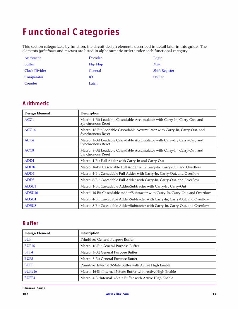
Functional CategoriesThis section categorizes, by function, the circuit design elements described in detail later in this guide. Theelements (primitives and macros) are listed in alphanumeric order under each functional category.
Arithmetic Decoder Logic
Buffer Flip Flop Mux
Clock Divider General Shift Register
Comparator IO Shifter
Counter Latch
ArithmeticDesign Element Description
ACC1 Macro: 1-Bit Loadable Cascadable Accumulator with Carry-In, Carry-Out, andSynchronous Reset
ACC16 Macro: 16-Bit Loadable Cascadable Accumulator with Carry-In, Carry-Out, andSynchronous Reset
ACC4 Macro: 4-Bit Loadable Cascadable Accumulator with Carry-In, Carry-Out, andSynchronous Reset
ACC8 Macro: 8-Bit Loadable Cascadable Accumulator with Carry-In, Carry-Out, andSynchronous Reset
ADD1 Macro: 1-Bit Full Adder with Carry-In and Carry-Out
ADD16 Macro: 16-Bit Cascadable Full Adder with Carry-In, Carry-Out, and Overflow
ADD4 Macro: 4-Bit Cascadable Full Adder with Carry-In, Carry-Out, and Overflow
ADD8 Macro: 8-Bit Cascadable Full Adder with Carry-In, Carry-Out, and Overflow
ADSU1 Macro: 1-Bit Cascadable Adder/Subtracter with Carry-In, Carry-Out
ADSU16 Macro: 16-Bit Cascadable Adder/Subtracter with Carry-In, Carry-Out, and Overflow
ADSU4 Macro: 4-Bit Cascadable Adder/Subtracter with Carry-In, Carry-Out, and Overflow
ADSU8 Macro: 8-Bit Cascadable Adder/Subtracter with Carry-In, Carry-Out, and Overflow
BufferDesign Element Description
BUF Primitive: General Purpose Buffer
BUF16 Macro: 16-Bit General Purpose Buffer
BUF4 Macro: 4-Bit General Purpose Buffer
BUF8 Macro: 8-Bit General Purpose Buffer
BUFE Primitive: Internal 3-State Buffer with Active High Enable
BUFE16 Macro: 16-Bit Internal 3-State Buffer with Active High Enable
BUFE4 Macro: 4-BitInternal 3-State Buffer with Active High Enable
Libraries Guide
10.1 www.xilinx.com 13

Functional Categories
Design Element Description
BUFE8 Macro: 8-Bit Internal 3-State Buffer with Active High Enable
BUFG Primitive: Global Clock Buffer
BUFGSR Primitive: Global Set/Reset Input Buffer
BUFGTS Primitive: Global 3-State Input Buffer
BUFT Primitive: Internal 3-State Buffer with Active Low Enable
BUFT16 Macro: 16-Bit Internal 3-State Buffers with Active Low Enable
BUFT4 Macro: 4-Bit Internal 3-State Buffers with Active Low Enable
BUFT8 Macro: 8-Bit Internal 3-State Buffers with Active Low Enable
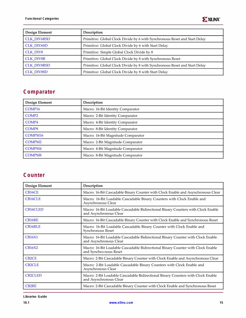
Clock Divider
Design Element Description
CLK_DIV10 Primitive: Simple Global Clock Divide by 10
CLK_DIV10R Primitive: Global Clock Divide by 10 with Synchronous Reset
CLK_DIV10RSD Primitive: Global Clock Divide by 10 with Synchronous Reset and Start Delay
CLK_DIV10SD Primitive: Global Clock Divide by 10 with Start Delay
CLK_DIV12 Primitive: Simple Global Clock Divide by 12
CLK_DIV12R Primitive: Global Clock Divide by 12 with Synchronous Reset
CLK_DIV12RSD Primitive: Global Clock Divide by 12 with Synchronous Reset and Start Delay
CLK_DIV12SD Primitive: Global Clock Divide by 12 with Start Delay
CLK_DIV14 Primitive: Simple Global Clock Divide by 14
CLK_DIV14R Primitive: Global Clock Divide by 14 with Synchronous Reset
CLK_DIV14RSD Primitive: Global Clock Divide by 14 with Synchronous Reset and Start Delay
CLK_DIV14SD Primitive: Global Clock Divide by 14 with Start Delay
CLK_DIV16 Primitive: Simple Global Clock Divide by 16
CLK_DIV16R Primitive: Global Clock Divide by 16 with Synchronous Reset
CLK_DIV16RSD Primitive: Global Clock Divide by 16 with Synchronous Reset and Start Delay
CLK_DIV16SD Primitive: Global Clock Divide by 16 with Start Delay
CLK_DIV2 Primitive: Simple Global Clock Divide by 2
CLK_DIV2R Primitive: Global Clock Divide by 2 with Synchronous Reset
CLK_DIV2RSD Primitive: Global Clock Divide by 2 with Synchronous Reset and Start Delay
CLK_DIV2SD Primitive: Global Clock Divide by 2 with Start Delay
CLK_DIV4 Primitive: Simple Global Clock Divide by 4
CLK_DIV4R Primitive: Global Clock Divide by 4 with Synchronous Reset
CLK_DIV4RSD Primitive: Global Clock Divide by 4 with Synchronous Reset and Start Delay
CLK_DIV4SD Primitive: Global Clock Divide by 4 with Start Delay
CLK_DIV6 Primitive: Simple Global Clock Divide by 6
CLK_DIV6R Primitive: Global Clock Divide by 6 with Synchronous Reset
Libraries Guide
14 www.xilinx.com 10.1
Functional Categories
Design Element Description
CLK_DIV6RSD Primitive: Global Clock Divide by 6 with Synchronous Reset and Start Delay
CLK_DIV6SD Primitive: Global Clock Divide by 6 with Start Delay
CLK_DIV8 Primitive: Simple Global Clock Divide by 8
CLK_DIV8R Primitive: Global Clock Divide by 8 with Synchronous Reset
CLK_DIV8RSD Primitive: Global Clock Divide by 8 with Synchronous Reset and Start Delay
CLK_DIV8SD Primitive: Global Clock Divide by 8 with Start Delay
Comparator
Design Element Description
COMP16 Macro: 16-Bit Identity Comparator
COMP2 Macro: 2-Bit Identity Comparator
COMP4 Macro: 4-Bit Identity Comparator
COMP8 Macro: 8-Bit Identity Comparator
COMPM16 Macro: 16-Bit Magnitude Comparator
COMPM2 Macro: 2-Bit Magnitude Comparator
COMPM4 Macro: 4-Bit Magnitude Comparator
COMPM8 Macro: 8-Bit Magnitude Comparator
Counter
Design Element Description
CB16CE Macro: 16-Bit Cascadable Binary Counter with Clock Enable and Asynchronous Clear
CB16CLE Macro: 16-Bit Loadable Cascadable Binary Counters with Clock Enable andAsynchronous Clear
CB16CLED Macro: 16-Bit Loadable Cascadable Bidirectional Binary Counters with Clock Enableand Asynchronous Clear
CB16RE Macro: 16-Bit Cascadable Binary Counter with Clock Enable and Synchronous Reset
CB16RLE Macro: 16-Bit Loadable Cascadable Binary Counter with Clock Enable andSynchronous Reset
CB16X1 Macro: 16-Bit Loadable Cascadable Bidirectional Binary Counter with Clock Enableand Asynchronous Clear
CB16X2 Macro: 16-Bit Loadable Cascadable Bidirectional Binary Counter with Clock Enableand Synchro-nous Reset
CB2CE Macro: 2-Bit Cascadable Binary Counter with Clock Enable and Asynchronous Clear
CB2CLE Macro: 2-Bit Loadable Cascadable Binary Counters with Clock Enable andAsynchronous Clear
CB2CLED Macro: 2-Bit Loadable Cascadable Bidirectional Binary Counters with Clock Enableand Asynchronous Clear
CB2RE Macro: 2-Bit Cascadable Binary Counter with Clock Enable and Synchronous Reset
Libraries Guide
10.1 www.xilinx.com 15

Functional Categories
Design Element Description
CB2RLE Macro: 2-Bit Loadable Cascadable Binary Counter with Clock Enable and SynchronousReset
CB2X1 Macro: 2-Bit Loadable Cascadable Bidirectional Binary Counter with Clock Enableand Asynchronous Clear
CB2X2 Macro: 2-Bit Loadable Cascadable Bidirectional Binary Counter with Clock Enableand Synchronous Reset
CB4CE Macro: 4-Bit Cascadable Binary Counter with Clock Enable and Asynchronous Clear
CB4CLE Macro: 4-Bit Loadable Cascadable Binary Counters with Clock Enable andAsynchronous Clear
CB4CLED Macro: 4-Bit Loadable Cascadable Bidirectional Binary Counters with Clock Enableand Asynchronous Clear
CB4RE Macro: 4-Bit Cascadable Binary Counter with Clock Enable and Synchronous Reset
CB4RLE Macro: 4-Bit Loadable Cascadable Binary Counter with Clock Enable and SynchronousReset
CB4X1 Macro: 4-Bit Loadable Cascadable Bidirectional Binary Counter with Clock Enableand Asynchronous Clear
CB4X2 Macro: 4-Bit Loadable Cascadable Bidirectional Binary Counter with Clock Enableand Synchronous Reset
CB8CE Macro: 8-Bit Cascadable Binary Counter with Clock Enable and Asynchronous Clear
CB8CLE Macro: 8-Bit Loadable Cascadable Binary Counters with Clock Enable andAsynchronous Clear
CB8CLED Macro: 8-Bit Loadable Cascadable Bidirectional Binary Counters with Clock Enableand Asynchronous Clear
CB8RE Macro: 8-Bit Cascadable Binary Counter with Clock Enable and Synchronous Reset
CB8RLE Macro: 8-Bit Loadable Cascadable Binary Counter with Clock Enable and SynchronousReset
CB8X1 Macro: 8-Bit Loadable Cascadable Bidirectional Binary Counter with Clock Enableand Asynchronous Clear
CB8X2 Macro: 8-Bit Loadable Cascadable Bidirectional Binary Counter with Clock Enableand Synchronous Reset
CBD16CE Macro: 16-Bit Cascadable Dual Edge Triggered Binary Counter with Clock Enableand Asynchronous Clear
CBD16CLE Macro: 16-Bit Loadable Cascadable Dual Edge Triggered Binary Counter with ClockEnable and Asynchronous Clear
CBD16CLED Macro: 16-Bit Loadable Cascadable Bidirectional Dual Edge Triggered Binary Counterwith Clock Enable and Asynchronous Clear
CBD16RE Macro: 16-Bit Cascadable Dual Edge Triggered Binary Counter with Clock Enableand Synchronous Reset
CBD16RLE Macro: 16-Bit Loadable Cascadable Dual Edge Triggered Binary Counter with ClockEnable and Synchronous Reset
CBD16X1 Macro: 16-Bit Loadable Cascadable Bidirectional Dual Edge Triggered Binary Counterwith Clock Enable and Asynchronous Clear
CBD16X2 Macro: 16-Bit Loadable Cascadable Bidirectional Dual Edge Triggered Binary Counterwith Clock Enable and Synchronous Reset
CBD2CE Macro: 2-Bit Cascadable Dual Edge Triggered Binary Counter with Clock Enableand Asynchronous Clear
Libraries Guide
16 www.xilinx.com 10.1

Functional Categories
Design Element Description
CBD2CLE Macro: 2-Bit Loadable Cascadable Dual Edge Triggered Binary Counter with ClockEnable and Asynchronous Clear
CBD2CLED Macro: 2-Bit Loadable Cascadable Bidirectional Dual Edge Triggered Binary Counterwith Clock Enable and Asynchronous Clear
CBD2RE Macro: 2-Bit Cascadable Dual Edge Triggered Binary Counter with Clock Enableand Synchronous Reset
CBD2RLE Macro: 2-Bit Loadable Cascadable Dual Edge Triggered Binary Counter with ClockEnable and Synchronous Reset
CBD2X1 Macro: 2-Bit Loadable Cascadable Bidirectional Dual Edge Triggered Binary Counterwith Clock Enable and Asynchronous Clear
CBD2X2 Macro: 2-Bit Loadable Cascadable Bidirectional Dual Edge Triggered Binary Counterwith Clock Enable and Synchronous Reset
CBD4CE Macro: 4-Bit Cascadable Dual Edge Triggered Binary Counter with Clock Enableand Asynchronous Clear
CBD4CLE Macro: 4-Bit Loadable Cascadable Dual Edge Triggered Binary Counter with ClockEnable and Asynchronous Clear
CBD4CLED Macro: 4-Bit Loadable Cascadable Bidirectional Dual Edge Triggered Binary Counterwith Clock Enable and Asynchronous Clear
CBD4RE Macro: 4-Bit Cascadable Dual Edge Triggered Binary Counter with Clock Enableand Synchronous Reset
CBD4RLE Macro: 4-Bit Loadable Cascadable Dual Edge Triggered Binary Counter with ClockEnable and Synchronous Reset
CBD4X1 Macro: 4-Bit Loadable Cascadable Bidirectional Dual Edge Triggered Binary Counterwith Clock Enable and Asynchronous Clear
CBD4X2 Macro: 4-Bit Loadable Cascadable Bidirectional Dual Edge Triggered Binary Counterwith Clock Enable and Synchronous Reset
CBD8CE Macro: 8-Bit Cascadable Dual Edge Triggered Binary Counter with Clock Enableand Asynchronous Clear
CBD8CLE Macro: 8-Bit Loadable Cascadable Dual Edge Triggered Binary Counter with ClockEnable and Asynchronous Clear
CBD8CLED Macro: 8-Bit Loadable Cascadable Bidirectional Dual Edge Triggered Binary Counterwith Clock Enable and Asynchronous Clear
CBD8RE Macro: 8-Bit Cascadable Dual Edge Triggered Binary Counter with Clock Enableand Synchronous Reset
CBD8RLE Macro: 8-Bit Loadable Cascadable Dual Edge Triggered Binary Counter with ClockEnable and Synchronous Reset
CBD8X1 Macro: 8-Bit Loadable Cascadable Bidirectional Dual Edge Triggered Binary Counterwith Clock Enable and Asynchronous Clear
CBD8X2 Macro: 8-Bit Loadable Cascadable Bidirectional Dual Edge Triggered Binary Counterwith Clock Enable and Synchronous Reset
CD4CE Macro: 4-Bit Cascadable BCD Counter with Clock Enable and Asynchronous Clear
CD4CLE Macro: 4-Bit Loadable Cascadable BCD Counter with Clock Enable and AsynchronousClear
CD4RE Macro: 4-Bit Cascadable BCD Counter with Clock Enable and Synchronous Reset
CD4RLE Macro: 4-Bit Loadable Cascadable BCD Counter with Clock Enable and SynchronousReset
Libraries Guide
10.1 www.xilinx.com 17

Functional Categories
Design Element Description
CDD4CE Macro: 4-Bit Cascadable Dual Edge Triggered BCD Counter with Clock Enable andAsynchronous Clear
CDD4CLE Macro: 4-Bit Loadable Cascadable Dual Edge Triggered BCD Counter with ClockEnable and Asynchronous Clear
CDD4RE Macro: 4-Bit Cascadable Dual Edge Triggered BCD Counter with Clock Enable andSynchronous Reset
CDD4RLE Macro: 4-Bit Loadable Cascadable Dual Edge Triggered BCD Counter with ClockEnable and Synchronous Reset
CJ4CE Macro: 4-Bit Johnson Counter with Clock Enable and Asynchronous Clear
CJ4RE Macro: 4-Bit Johnson Counter with Clock Enable and Synchronous Reset
CJ5CE Macro: 5-Bit Johnson Counter with Clock Enable and Asynchronous Clear
CJ5RE Macro: 5-Bit Johnson Counter with Clock Enable and Synchronous Reset
CJ8CE Macro: 8-Bit Johnson Counter with Clock Enable and Asynchronous Clear
CJ8RE Macro: 8-Bit Johnson Counter with Clock Enable and Synchronous Reset
CJD4CE Macro: 4-Bit Dual Edge Triggered Johnson Counter with Clock Enable andAsynchronous Clear
CJD4RE Macro: 4-Bit Dual Edge Triggered Johnson Counter with Clock Enable andSynchronous Reset
CJD5CE Macro: 5-Bit Dual Edge Triggered Johnson Counter with Clock Enable andAsynchronous Clear
CJD5RE Macro: 5-Bit Dual Edge Triggered Johnson Counter with Clock Enable andSynchronous Reset
CJD8CE Macro: 8-Bit Dual Edge Triggered Johnson Counter with Clock Enable andAsynchronous Clear
CJD8RE Macro: 8-Bit Dual Edge Triggered Johnson Counter with Clock Enable andSynchronous Reset
CR16CE Macro: 16-Bit Negative-Edge Binary Ripple Counter with Clock Enable andAsynchronous Clear
CR8CE Macro: 8-Bit Negative-Edge Binary Ripple Counter with Clock Enable andAsynchronous Clear
CRD16CE Macro: 16-Bit Dual-Edge Triggered Binary Ripple Counter with Clock Enable andAsynchronous Clear
CRD8CE Macro: 8-Bit Dual-Edge Triggered Binary Ripple Counter with Clock Enable andAsynchronous Clear
Decoder
Design Element Description
D2_4E Macro: 2- to 4-Line Decoder/Demultiplexer with Enable
D3_8E Macro: 3- to 8-Line Decoder/Demultiplexer with Enable
D4_16E Macro: 4- to 16-Line Decoder/Demultiplexer with Enable
Libraries Guide
18 www.xilinx.com 10.1

Functional Categories
Flip Flop
Design Element Description
FD Macro: D Flip-Flop
FD16 Macro: Multiple D Flip-Flop
FD16CE Macro: 16-Bit Data Register with Clock Enable and Asynchronous Clear
FD16RE Macro: 16-Bit Data Register with Clock Enable and Synchronous Reset
FD4 Macro: Multiple D Flip-Flop
FD4CE Macro: 4-Bit Data Register with Clock Enable and Asynchronous Clear
FD4RE Macro: 4-Bit Data Register with Clock Enable and Synchronous Reset
FD8 Macro: Multiple D Flip-Flop
FD8CE Macro: 8-Bit Data Register with Clock Enable and Asynchronous Clear
FD8RE Macro: 8-Bit Data Register with Clock Enable and Synchronous Reset
FDC Macro: D Flip-Flop with Asynchronous Clear
FDCE Primitive: D Flip-Flop with Clock Enable and Asynchronous Clear
FDCP Primitive: D Flip-Flop with Asynchronous Preset and Clear
FDCPE Primitive: D Flip-Flop with Clock Enable and Asynchronous Preset and Clear
FDD Macro: Dual Edge Triggered D Flip-Flop
FDD16 Macro: Multiple Dual Edge Triggered D Flip-Flop
FDD16CE Macro: 16-Bit Dual Edge Triggered Data Register with Clock Enable and AsynchronousClear
FDD16RE Macro: 16-Bit Dual Edge Triggered Data Register with Clock Enable and SynchronousReset
FDD4 Macro: Multiple Dual Edge Triggered D Flip-Flop
FDD4CE Macro: 4-Bit Dual Edge Triggered Data Register with Clock Enable and AsynchronousClear
FDD4RE Macro: 4-Bit Dual Edge Triggered Data Register with Clock Enable and SynchronousReset
FDD8 Macro: Multiple Dual Edge Triggered D Flip-Flop
FDD8CE Macro: 8-Bit Dual Edge Triggered Data Register with Clock Enable and AsynchronousClear
FDD8RE Macro: 8-Bit Dual Edge Triggered Data Register with Clock Enable and SynchronousReset
FDDC Macro: D Dual Edge Triggered Flip-Flop with Asynchronous Clear
FDDCE Primitive: Dual Edge Triggered D Flip-Flop with Clock Enable and AsynchronousClear
FDDCP Primitive: Dual Edge Triggered D Flip-Flop Asynchronous Preset and Clear
FDDCPE Macro: Dual Edge Triggered D Flip-Flop with Clock Enable and Asynchronous Presetand Clear
FDDP Macro: Dual Edge Triggered D Flip-Flop with Asynchronous Preset
FDDPE Primitive: Dual Edge Triggered D Flip-Flop with Clock Enable and AsynchronousPreset
FDDR Macro: Dual Edge Triggered D Flip-Flop with Synchronous Reset
Libraries Guide
10.1 www.xilinx.com 19

Functional Categories
Design Element Description
FDDRE Macro: Dual Edge Triggered D Flip-Flop with Clock Enable and Synchronous Reset
FDDRS Macro: Dual Edge Triggered D Flip-Flop with Synchronous Reset and Set
FDDRSE Macro: Dual Edge Triggered D Flip-Flop with Synchronous Reset and Set and ClockEnable
FDDS Macro: Dual Edge Triggered D Flip-Flop with Synchronous Set
FDDSE Macro: D Flip-Flop with Clock Enable and Synchronous Set
FDDSR Macro: Dual Edge Triggered D Flip-Flop with Synchronous Set and Reset
FDDSRE Macro: Dual Edge Triggered D Flip-Flop with Synchronous Set and Reset and ClockEnable
FDP Macro: D Flip-Flop with Asynchronous Preset
FDPE Primitive: D Flip-Flop with Clock Enable and Asynchronous Preset
FDR Macro: D Flip-Flop with Synchronous Reset
FDRE Macro: D Flip-Flop with Clock Enable and Synchronous Reset
FDRS Macro: D Flip-Flop with Synchronous Reset and Set
FDRSE Macro: D Flip-Flop with Synchronous Reset and Set and Clock Enable
FDS Macro: D Flip-Flop with Synchronous Set
FDSE Macro: D Flip-Flop with Clock Enable and Synchronous Set
FDSR Macro: D Flip-Flop with Synchronous Set and Reset
FDSRE Macro: D Flip-Flop with Synchronous Set and Reset and Clock Enable
FJKC Macro: J-K Flip-Flop with Asynchronous Clear
FJKCE Macro: J-K Flip-Flop with Clock Enable and Asynchronous Clear
FJKCP Macro: J-K Flip-Flop with Asynchronous Clear and Preset
FJKCPE Macro: J-K Flip-Flop with Asynchronous Clear and Preset and Clock Enable
FJKP Macro: J-K Flip-Flop with Asynchronous Preset
FJKPE Macro: J-K Flip-Flop with Clock Enable and Asynchronous Preset
FJKRSE Macro: J-K Flip-Flop with Clock Enable and Synchronous Reset and Set
FJKSRE Macro: J-K Flip-Flop with Clock Enable and Synchronous Set and Reset
FTC Macro: Toggle Flip-Flop with Asynchronous Clear
FTCE Macro: Toggle Flip-Flop with Clock Enable and Asynchronous Clear
FTCLE Macro: Toggle/Loadable Flip-Flop with Clock Enable and Asynchronous Clear
FTCLEX Macro: Toggle/Loadable Flip-Flop with Clock Enable and Asynchronous Clear
FTCP Primitive: Toggle Flip-Flop with Asynchronous Clear and Preset
FTCPE Macro: Toggle Flip-Flop with Clock Enable and Asynchronous Clear and Preset
FTCPLE Macro: Loadable Toggle Flip-Flop with Clock Enable and Asynchronous Clear andPreset
FTDCE Macro: Dual-Edge Triggered Toggle Flip-Flop with Clock Enable and AsynchronousClear
FTDCLE Macro: Dual-Edge Triggered Toggle/Loadable Flip-Flop with Clock Enable andAsynchronous Clear
Libraries Guide
20 www.xilinx.com 10.1

Functional Categories
Design Element Description
FTDCLEX Macro: Dual-Edge Triggered Toggle/Loadable Flip-Flop with Clock Enable andAsynchronous Clear
FTDCP Primitive: Dual-Edge Triggered Toggle Flip-Flop with Asynchronous Clear and Preset
FTDRSE Macro: Dual-Edge Triggered Toggle Flip-Flop with Synchronous Reset, Set, andClock Enable
FTDRSLE Macro: Dual-Edge Triggered Toggle Flip-Flop with Clock Enable and SynchronousReset and Set
FTP Macro: Toggle Flip-Flop with Asynchronous Preset
FTPE Macro: Toggle Flip-Flop with Clock Enable and Asynchronous Preset
FTPLE Macro: Toggle/Loadable Flip-Flop with Clock Enable and Asynchronous Preset
FTRSE Macro: Toggle Flip-Flop with Clock Enable and Synchronous Reset and Set
FTRSLE Macro: Toggle/Loadable Flip-Flop with Clock Enable and Synchronous Reset and Set
FTSRE Macro: Toggle Flip-Flop with Clock Enable and Synchronous Set and Reset
FTSRLE Macro: Toggle/Loadable Flip-Flop with Clock Enable and Synchronous Set and Reset
GeneralDesign Element Description
GND Primitive: Ground-Connection Signal Tag
KEEPER Primitive: KEEPER Symbol
PULLDOWN Primitive: Resistor to GND for Input Pads, Open-Drain, and 3-State Outputs
PULLUP Primitive: Resistor to VCC for Input PADs, Open-Drain, and 3-State Outputs
VCC Primitive: VCC-Connection Signal Tag
IODesign Element Description
IBUF Primitive: Input Buffer
IBUF16 Macro: 16-Bit Input Buffer
IBUF4 Macro: 4-Bit Input Buffer
IBUF8 Macro: 8-Bit Input Buffer
IOBUFE Primitive: Bi-Directional Buffer
OBUF Primitive: Output Buffer
OBUF16 Macro: 16-Bit Output Buffer
OBUF4 Macro: 4-Bit Output Buffer
OBUF8 Macro: 8-Bit Output Buffer
OBUFE Macro: 3-State Output Buffer with Active-High Output Enable
OBUFE16 Macro: 16-Bit 3-State Output Buffer with Active-High Output Enable
OBUFE4 Macro: 4-Bit 3-State Output Buffer with Active-High Output Enable
Libraries Guide
10.1 www.xilinx.com 21

Functional Categories
Design Element Description
OBUFE8 Macro: 8-Bit 3-State Output Buffer with Active-High Output Enable
OBUFT Primitive: 3-State Output Buffer with Active Low Output Enable
OBUFT16 Macro: 16-Bit 3-State Output Buffer with Active Low Output Enable
OBUFT4 Macro: 4-Bit 3-State Output Buffers with Active-Low Output Enable
OBUFT8 Macro: 8-Bit 3-State Output Buffers with Active-Low Output Enable
LatchDesign Element Description
LD Primitive: Transparent Data Latch
LD16 Macro: Multiple Transparent Data Latch
LD4 Macro: Multiple Transparent Data Latch
LD8 Macro: Multiple Transparent Data Latch
LDC Macro: Transparent Data Latch with Asynchronous Clear
LDCP Primitive: Transparent Data Latch with Asynchronous Clear and Preset
LDG Primitive: Transparent Datagate Latch
LDG16 Macro: 16-bit Transparent Datagate Latch
LDG4 Macro: 4-Bit Transparent Datagate Latch
LDG8 Macro: 8-Bit Transparent Datagate Latch
LDP Macro: Transparent Data Latch with Asynchronous Preset
LogicDesign Element Description
AND2 Primitive: 2-Input AND Gate with Non-Inverted Inputs
AND2B1 Primitive: 2-Input AND Gate with 1 Inverted and 1 Non-Inverted Inputs
AND2B2 Primitive: 2-Input AND Gate with Inverted Inputs
AND3 Primitive: 3-Input AND Gate with Non-Inverted Inputs
AND3B1 Primitive: 3-Input AND Gate with 1 Inverted and 2 Non-Inverted Inputs
AND3B2 Primitive: 3-Input AND Gate with 2 Inverted and 1 Non-Inverted Inputs
AND3B3 Primitive: 3-Input AND Gate with Inverted Inputs
AND4 Primitive: 4-Input AND Gate with Non-Inverted Inputs
AND4B1 Primitive: 4-Input AND Gate with 1 Inverted and 3 Non-Inverted Inputs
AND4B2 Primitive: 4-Input AND Gate with 2 Inverted and 2 Non-Inverted Inputs
AND4B3 Primitive: 4-Input AND Gate with 3 Inverted and 1 Non-Inverted Inputs
AND4B4 Primitive: 4-Input AND Gate with Inverted Inputs
AND5 Primitive: 5-Input AND Gate with Non-Inverted Inputs
AND5B1 Primitive: 5-Input AND Gate with 1 Inverted and 4 Non-Inverted Inputs
Libraries Guide
22 www.xilinx.com 10.1

Functional Categories
Design Element Description
AND5B2 Primitive: 5-Input AND Gate with 2 Inverted and 3 Non-Inverted Inputs
AND5B3 Primitive: 5-Input AND Gate with 3 Inverted and 2 Non-Inverted Inputs
AND5B4 Primitive: 5-Input AND Gate with 4 Inverted and 1 Non-Inverted Inputs
AND5B5 Primitive: 5-Input AND Gate with Inverted Inputs
AND6 Macro: 6-Input AND Gate with Non-Inverted Inputs
AND7 Macro: 7-Input AND Gate with Non-Inverted Inputs
AND8 Macro: 8-Input AND Gate with Non-Inverted Inputs
AND9 Macro: 9-Input AND Gate with Non-Inverted Inputs
INV Primitive: Inverter
INV16 Macro: 16 Inverters
INV4 Macro: Four Inverters
INV8 Macro: Eight Inverters
NAND2 Primitive: 2-Input NAND Gate with Non-Inverted Inputs
NAND2B1 Primitive: 2-Input NAND Gate with 1 Inverted and 1 Non-Inverted Inputs
NAND2B2 Primitive: 2-Input NAND Gate with Inverted Inputs
NAND3 Primitive: 3-Input NAND Gate with Non-Inverted Inputs
NAND3B1 Primitive: 3-Input NAND Gate with 1 Inverted and 2 Non-Inverted Inputs
NAND3B2 Primitive: 3-Input NAND Gate with 2 Inverted and 1 Non-Inverted Inputs
NAND3B3 Primitive: 3-Input NAND Gate with Inverted Inputs
NAND4 Primitive: 4-Input NAND Gate with Non-Inverted Inputs
NAND4B1 Primitive: 4-Input NAND Gate with 1 Inverted and 3 Non-Inverted Inputs
NAND4B2 Primitive: 4-Input NAND Gate with 2 Inverted and 2 Non-Inverted Inputs
NAND4B3 Primitive: 4-Input NAND Gate with 3 Inverted and 1 Non-Inverted Inputs
NAND4B4 Primitive: 4-Input NAND Gate with Inverted Inputs
NAND5 Primitive: 5-Input NAND Gate with Non-Inverted Inputs
NAND5B1 Primitive: 5-Input NAND Gate with 1 Inverted and 4 Non-Inverted Inputs
NAND5B2 Primitive: 5-Input NAND Gate with 2 Inverted and 3 Non-Inverted Inputs
NAND5B3 Primitive: 5-Input NAND Gate with 3 Inverted and 2 Non-Inverted Inputs
NAND5B4 Primitive: 5-Input NAND Gate with 4 Inverted and 1 Non-Inverted Inputs
NAND5B5 Primitive: 5-Input NAND Gate with Inverted Inputs
NAND6 Macro: 6-Input NAND Gate with Non-Inverted Inputs
NAND7 Macro: 7-Input NAND Gate with Non-Inverted Inputs
NAND8 Macro: 8-Input NAND Gate with Non-Inverted Inputs
NAND9 Macro: 9-Input NAND Gate with Non-Inverted Inputs
NOR2 Primitive: 2-Input NOR Gate with Non-Inverted Inputs
NOR2B1 Primitive: 2-Input NOR Gate with 1 Inverted and 1 Non-Inverted Inputs
NOR2B2 Primitive: 2-Input NOR Gate with Inverted Inputs
NOR3 Primitive: 3-Input NOR Gate with Non-Inverted Inputs
Libraries Guide
10.1 www.xilinx.com 23

Functional Categories
Design Element Description
NOR3B1 Primitive: 3-Input NOR Gate with 1 Inverted and 2 Non-Inverted Inputs
NOR3B2 Primitive: 3-Input NOR Gate with 2 Inverted and 1 Non-Inverted Inputs
NOR3B3 Primitive: 3-Input NOR Gate with Inverted Inputs
NOR4 Primitive: 4-Input NOR Gate with Non-Inverted Inputs
NOR4B1 Primitive: 4-Input NOR Gate with 1 Inverted and 3 Non-Inverted Inputs
NOR4B2 Primitive: 4-Input NOR Gate with 2 Inverted and 2 Non-Inverted Inputs
NOR4B3 Primitive: 4-Input NOR Gate with 3 Inverted and 1 Non-Inverted Inputs
NOR4B4 Primitive: 4-Input NOR Gate with Inverted Inputs
NOR5 Primitive: 5-Input NOR Gate with Non-Inverted Inputs
NOR5B1 Primitive: 5-Input NOR Gate with 1 Inverted and 4 Non-Inverted Inputs
NOR5B2 Primitive: 5-Input NOR Gate with 2 Inverted and 3 Non-Inverted Inputs
NOR5B3 Primitive: 5-Input NOR Gate with 3 Inverted and 2 Non-Inverted Inputs
NOR5B4 Primitive: 5-Input NOR Gate with 4 Inverted and 1 Non-Inverted Inputs
NOR5B5 Primitive: 5-Input NOR Gate with Inverted Inputs
NOR6 Macro: 6-Input NOR Gate with Non-Inverted Inputs
NOR7 Macro: 7-Input NOR Gate with Non-Inverted Inputs
NOR8 Macro: 8-Input NOR Gate with Non-Inverted Inputs
NOR9 Macro: 9-Input NOR Gate with Non-Inverted Inputs
OR2 Primitive: 2-Input OR Gate with Non-Inverted Inputs
OR2B1 Primitive: 2-Input OR Gate with 1 Inverted and 1 Non-Inverted Inputs
OR2B2 Primitive: 2-Input OR Gate with Inverted Inputs
OR3 Primitive: 3-Input OR Gate with Non-Inverted Inputs
OR3B1 Primitive: 3-Input OR Gate with 1 Inverted and 2 Non-Inverted Inputs
OR3B2 Primitive: 3-Input OR Gate with 2 Inverted and 1 Non-Inverted Inputs
OR3B3 Primitive: 3-Input OR Gate with Inverted Inputs
OR4 Primitive: 4-Input OR Gate with Non-Inverted Inputs
OR4B1 Primitive: 4-Input OR Gate with 1 Inverted and 3 Non-Inverted Inputs
OR4B2 Primitive: 4-Input OR Gate with 2 Inverted and 2 Non-Inverted Inputs
OR4B3 Primitive: 4-Input OR Gate with 3 Inverted and 1 Non-Inverted Inputs
OR4B4 Primitive: 4-Input OR Gate with Inverted Inputs
OR5 Primitive: 5-Input OR Gate with Non-Inverted Inputs
OR5B1 Primitive: 5-Input OR Gate with 1 Inverted and 4 Non-Inverted Inputs
OR5B2 Primitive: 5-Input OR Gate with 2 Inverted and 3 Non-Inverted Inputs
OR5B3 Primitive: 5-Input OR Gate with 3 Inverted and 2 Non-Inverted Inputs
OR5B4 Primitive: 5-Input OR Gate with 4 Inverted and 1 Non-Inverted Inputs
OR5B5 Primitive: 5-Input OR Gate with Inverted Inputs
OR6 Macro: 6-Input OR Gate with Non-Inverted Inputs
OR7 Macro: 7-Input OR Gate with Non-Inverted Inputs
Libraries Guide
24 www.xilinx.com 10.1

Functional Categories
Design Element Description
OR8 Macro: 8-Input OR Gate with Non-Inverted Inputs
OR9 Macro: 9-Input OR Gate with Non-Inverted Inputs
XNOR2 Primitive: 2-Input XNOR Gate with Non-Inverted Inputs
XNOR3 Primitive: 3-Input XNOR Gate with Non-Inverted Inputs
XNOR4 Primitive: 4-Input XNOR Gate with Non-Inverted Inputs
XNOR5 Primitive: 5-Input XNOR Gate with Non-Inverted Inputs
XNOR6 Macro: 6-Input XNOR Gate with Non-Inverted Inputs
XNOR7 Macro: 7-Input XNOR Gate with Non-Inverted Inputs
XNOR8 Macro: 8-Input XNOR Gate with Non-Inverted Inputs
XNOR9 Macro: 9-Input XNOR Gate with Non-Inverted Inputs
XOR2 Primitive: 2-Input XOR Gate with Non-Inverted Inputs
XOR3 Primitive: 3-Input XOR Gate with Non-Inverted Inputs
XOR4 Primitive: 4-Input XOR Gate with Non-Inverted Inputs
XOR5 Primitive: 5-Input XOR Gate with Non-Inverted Inputs
XOR6 Macro: 6-Input XOR Gate with Non-Inverted Inputs
XOR7 Macro: 7-Input XOR Gate with Non-Inverted Inputs
XOR8 Macro: 8-Input XOR Gate with Non-Inverted Inputs
XOR9 Macro: 9-Input XOR Gate with Non-Inverted Inputs
Mux
Design Element Description
M16_1E Macro: 16-to-1 Multiplexer with Enable
M2_1 Macro: 2-to-1 Multiplexer
M2_1B1 Macro: 2-to-1 Multiplexer with D0 Inverted
M2_1B2 Macro: 2-to-1 Multiplexer with D0 and D1 Inverted
M2_1E Macro: 2-to-1 Multiplexer with Enable
M4_1E Macro: 4-to-1 Multiplexer with Enable
M8_1E Macro: 8-to-1 Multiplexer with Enable
Shift Register
Design Element Description
SR16CE Macro: 16-Bit Serial-In Parallel-Out Shift Register with Clock Enable andAsynchronous Clear
SR16CLE Macro: 16-Bit Loadable Serial/Parallel-In Parallel-Out Shift Register with Clock Enableand Asynchronous Clear
SR16CLED Macro: 16-Bit Shift Register with Clock Enable and Asynchronous Clear
Libraries Guide
10.1 www.xilinx.com 25

Functional Categories
Design Element Description
SR16RE Macro: 16-Bit Serial-In Parallel-Out Shift Register with Clock Enable and SynchronousReset
SR16RLE Macro: 16-Bit Loadable Serial/Parallel-In Parallel-Out Shift Register with Clock Enableand Synchronous Reset
SR16RLED Macro: 16-Bit Shift Register with Clock Enable and Synchronous Reset
SR4CE Macro: 4-Bit Serial-In Parallel-Out Shift Register with Clock Enable and AsynchronousClear
SR4CLE Macro: 4-Bit Loadable Serial/Parallel-In Parallel-Out Shift Register with Clock Enableand Asynchronous Clear
SR4CLED Macro: 4-Bit Shift Register with Clock Enable and Asynchronous Clear
SR4RE Macro: 4-Bit Serial-In Parallel-Out Shift Register with Clock Enable and SynchronousReset
SR4RLE Macro: 4-Bit Loadable Serial/Parallel-In Parallel-Out Shift Register with Clock Enableand Synchronous Reset
SR4RLED Macro: 4-Bit Shift Register with Clock Enable and Synchronous Reset
SR8CE Macro: 8-Bit Serial-In Parallel-Out Shift Register with Clock Enable and AsynchronousClear
SR8CLE Macro: 8-Bit Loadable Serial/Parallel-In Parallel-Out Shift Register with Clock Enableand Asynchronous Clear
SR8CLED Macro: 8-Bit Shift Register with Clock Enable and Asynchronous Clear
SR8RE Macro: 8-Bit Serial-In Parallel-Out Shift Register with Clock Enable and SynchronousReset
SR8RLE Macro: 8-Bit Loadable Serial/Parallel-In Parallel-Out Shift Register with Clock Enableand Synchronous Reset
SR8RLED Macro: 8-Bit Shift Register with Clock Enable and Synchronous Reset
SRD16CE Macro: 16-Bit Serial-In Parallel-Out Dual Edge Triggered Shift Register with ClockEnable and Asynchronous Clear
SRD16CLE Macro: 16-Bit Loadable Serial/Parallel-In Parallel-Out Dual Edge Triggered ShiftRegister with Clock Enable and Asynchronous Clear
SRD16CLED Macro: 16-Bit Dual Edge Triggered Shift Register with Clock Enable and AsynchronousClear
SRD16RE Macro: 16-Bit Serial-In Parallel-Out Dual Edge Triggered Shift Register with ClockEnable and Synchronous Reset
SRD16RLE Macro: 16-Bit Loadable Serial/Parallel-In Parallel-Out Dual Edge Triggered ShiftRegister with Clock Enable and Synchronous Reset
SRD16RLED Macro: 16-Bit Dual Edge Triggered Shift Register with Clock Enable and SynchronousReset
SRD4CE Macro: 4-Bit Serial-In Parallel-Out Dual Edge Triggered Shift Register with ClockEnable and Asynchronous Clear
SRD4CLE Macro: 4-Bit Loadable Serial/Parallel-In Parallel-Out Dual Edge Triggered ShiftRegister with Clock Enable and Asynchronous Clear
SRD4CLED Macro: 4-Bit Dual Edge Triggered Shift Register with Clock Enable and AsynchronousClear
SRD4RE Macro: 4-Bit Serial-In Parallel-Out Dual Edge Triggered Shift Register with ClockEnable and Synchronous Reset
Libraries Guide
26 www.xilinx.com 10.1

Functional Categories
Design Element Description
SRD4RLE Macro: 4-Bit Loadable Serial/Parallel-In Parallel-Out Dual Edge Triggered ShiftRegister with Clock Enable and Synchronous Reset
SRD4RLED Macro: 4-Bit Dual Edge Triggered Shift Register with Clock Enable and SynchronousReset
SRD8CE Macro: 8-Bit Serial-In Parallel-Out Dual Edge Triggered Shift Register with ClockEnable and Asynchronous Clear
SRD8CLE Macro: 8-Bit Loadable Serial/Parallel-In Parallel-Out Dual Edge Triggered ShiftRegister with Clock Enable and Asynchronous Clear
SRD8CLED Macro: 8-Bit Dual Edge Triggered Shift Register with Clock Enable and AsynchronousClear
SRD8RE Macro: 8-Bit Serial-In Parallel-Out Dual Edge Triggered Shift Register with ClockEnable and Synchronous Reset
SRD8RLE Macro: 8-Bit Loadable Serial/Parallel-In Parallel-Out Dual Edge Triggered ShiftRegister with Clock Enable and Synchronous Reset
SRD8RLED Macro: 8-Bit Dual Edge Triggered Shift Register with Clock Enable and SynchronousReset
Shifter
Design Element Description
BRLSHFT4 Macro: 4-Bit Barrel Shifter
BRLSHFT8 Macro: 8-Bit Barrel Shifter
Libraries Guide
10.1 www.xilinx.com 27

Libraries Guide
28 www.xilinx.com 10.1

About Design ElementsThis section describes the design elements that can be used with this architecture. The design elements areorganized alphabetically.
The following information is provided for each design element, where applicable:
• Name of element
• Brief description
• Schematic symbol (if any)
• Logic Table (if any)
• Port Descriptions (if any)
• Design Entry Method
• Available Attributes (if any)
• For more information
You can find examples of VHDL and Verilog instantiation code in the ISE software (in the main menu, select Edit> Language Templates or in the Libraries Guide for HDL Designs for this architecture.
Libraries Guide
10.1 www.xilinx.com 29

About Design Elements
ACC1
Macro: 1-Bit Loadable Cascadable Accumulator with Carry-In, Carry-Out, and Synchronous Reset
Supported Architectures
This design element is supported in the following architectures only:
• XC9500XL
• CoolRunner XPLA3
• CoolRunner-II
IntroductionThis design element can add or subtract a 1-bit unsigned-binary word to or from the contents of a 1-bit dataregister and store the results in the register. The register can be loaded with a 1-bit word. The synchronous reset(R) has priority over all other inputs and, when High, causes the output to go to logic level zero during theLow-to-High clock (C) transition. Clock (C) transitions are ignored when clock enable (CE) is Low.
Load
When the load input (L) is High, CE is ignored and the data on the input D0 is loaded into the 1-bit registerduring the Low-to-High clock (C) transition.
Add
When control inputs ADD and CE are both High, the accumulator adds a 1-bit word (B0) and carry-in (CI) to thecontents of the 1-bit register. The result is stored in the register and appears on output Q0 during the Low-to-Highclock transition. The carry-out (CO) is not registered synchronously with the data output. CO always reflects theaccumulation of input B0 and the contents of the register, which allows cascading of ACC1s by connecting CO ofone stage to CI of the next stage. In add mode, CO acts as a carry-out, and CO and CI are active-High.
Subtract
When ADD is Low and CE is High, the 1-bit word B0 and CI are subtracted from the contents of the register. Theresult is stored in the register and appears on output Q0 during the Low-to-High clock transition. The carry-out(CO) is not registered synchronously with the data output. CO always reflects the accumulation of input B0 andthe contents of the register, which allows cascading of ACC1s by connecting CO of one stage to CI of the nextstage. In subtract mode, CO acts as a borrow, and CO and CI are active-Low.
This design element is asynchronously cleared, outputs Low, when power is applied. For CPLD devices, you cansimulate power-on by applying a High-level pulse on the PRLD global net.
Libraries Guide
30 www.xilinx.com 10.1

About Design Elements
Design Entry MethodThis design element is only for use in schematics.
For More Information• See the appropriate CPLD User Guide.
• See the appropriate CPLD Data Sheets.
Libraries Guide
10.1 www.xilinx.com 31

About Design Elements
ACC16
Macro: 16-Bit Loadable Cascadable Accumulator with Carry-In, Carry-Out, and Synchronous Reset
Supported ArchitecturesThis design element is supported in the following architectures only:• XC9500XL• CoolRunner XPLA3• CoolRunner-II
IntroductionThis design element can add or subtract a 16-bit unsigned-binary, respectively or twos-complement word toor from the contents of a 16-bit data register and store the results in the register. The register can be loadedwith the 16-bit word.
When the load input (L) is High, CE is ignored and the data on the D inputs is loaded into the register during theLow-to-High clock (C) transition. ACC16 loads the data on inputs D15 – D0 into the 16-bit register.
This design element operates on either 16-bit unsigned binary numbers or 16-bit twos-complement numbers. Ifthe inputs are interpreted as unsigned binary, the result can be interpreted as unsigned binary. If the inputsare interpreted as twos complement, the output can be interpreted as twos complement. The only functionaldifference between an unsigned binary operation and a twos-complement operation is how they determine when“overflow” occurs. Unsigned binary uses carry-out (CO), while twos complement uses OFL to determinewhen “overflow” occurs.• For unsigned binary operation, ACC16 can represent numbers between 0 and 15, inclusive. In add mode,
CO is active (High) when the sum exceeds the bounds of the adder/subtracter. In subtract mode, CO is anactive-Low borrow-out and goes Low when the difference exceeds the bounds. The carry-out (CO) isnot registered synchronously with the data outputs. CO always reflects the accumulation of the B inputs(B15 – B0 for ACC16). This allows the cascading of ACC16s by connecting CO of one stage to CI of thenext stage. An unsigned binary “overflow” that is always active-High can be generated by gating theADD signal and CO as follows:unsigned overflow = CO XOR ADD
Ignore OFL in unsigned binary operation.
Libraries Guide
32 www.xilinx.com 10.1
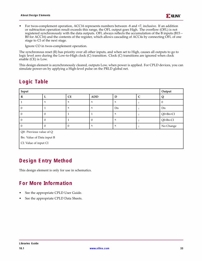
About Design Elements
• For twos-complement operation, ACC16 represents numbers between -8 and +7, inclusive. If an additionor subtraction operation result exceeds this range, the OFL output goes High. The overflow (OFL) is notregistered synchronously with the data outputs. OFL always reflects the accumulation of the B inputs (B15 –B0 for ACC16) and the contents of the register, which allows cascading of ACC4s by connecting OFL of onestage to CI of the next stage.
Ignore CO in twos-complement operation.
The synchronous reset (R) has priority over all other inputs, and when set to High, causes all outputs to go tologic level zero during the Low-to-High clock (C) transition. Clock (C) transitions are ignored when clockenable (CE) is Low.
This design element is asynchronously cleared, outputs Low, when power is applied. For CPLD devices, you cansimulate power-on by applying a High-level pulse on the PRLD global net.
Logic TableInput Output
R L CE ADD D C Q
1 x x x x ↑ 0
0 1 x x Dn ↑ Dn
0 0 1 1 x ↑ Q0+Bn+CI
0 0 1 0 x ↑ Q0-Bn-CI
0 0 0 x x ↑ No Change
Q0: Previous value of Q
Bn: Value of Data input B
CI: Value of input CI
Design Entry MethodThis design element is only for use in schematics.
For More Information• See the appropriate CPLD User Guide.
• See the appropriate CPLD Data Sheets.
Libraries Guide
10.1 www.xilinx.com 33

About Design Elements
ACC4
Macro: 4-Bit Loadable Cascadable Accumulator with Carry-In, Carry-Out, and Synchronous Reset
Supported Architectures
This design element is supported in the following architectures only:
• XC9500XL
• CoolRunner XPLA3
• CoolRunner-II
IntroductionThis design element can add or subtract a 4-bit unsigned-binary, respectively or twos-complement word to orfrom the contents of a 4-bit data register and store the results in the register. The register can be loaded with the4-bit word.
When the load input (L) is High, CE is ignored and the data on the D inputs is loaded into the register during theLow-to-High clock (C) transition. ACC4 loads the data on inputs D3 – D0 into the 4-bit register.
Libraries Guide
34 www.xilinx.com 10.1

About Design Elements
This design element operates on either 4-bit unsigned binary numbers or 4-bit twos-complement numbers. Ifthe inputs are interpreted as unsigned binary, the result can be interpreted as unsigned binary. If the inputsare interpreted as twos complement, the output can be interpreted as twos complement. The only functionaldifference between an unsigned binary operation and a twos-complement operation is how they determine when“overflow” occurs. Unsigned binary uses carry-out (CO), while twos complement uses OFL to determinewhen “overflow” occurs.
• For unsigned binary operation, ACC4 can represent numbers between 0 and 15, inclusive. In add mode,CO is active (High) when the sum exceeds the bounds of the adder/subtracter. In subtract mode, CO is anactive-Low borrow-out and goes Low when the difference exceeds the bounds. The carry-out (CO) isnot registered synchronously with the data outputs. CO always reflects the accumulation of the B inputs(B3 – B0 for ACC4). This allows the cascading of ACC4s by connecting CO of one stage to CI of the nextstage. An unsigned binary “overflow” that is always active-High can be generated by gating the ADDsignal and CO as follows:
unsigned overflow = CO XOR ADD
Ignore OFL in unsigned binary operation.
• For twos-complement operation, ACC4 represents numbers between -8 and +7, inclusive. If an additionor subtraction operation result exceeds this range, the OFL output goes High. The overflow (OFL) is notregistered synchronously with the data outputs. OFL always reflects the accumulation of the B inputs (B3 –B0 for ACC4) and the contents of the register, which allows cascading of ACC4s by connecting OFL of onestage to CI of the next stage.
Ignore CO in twos-complement operation.
The synchronous reset (R) has priority over all other inputs, and when set to High, causes all outputs to go tologic level zero during the Low-to-High clock (C) transition. Clock (C) transitions are ignored when clockenable (CE) is Low.
This design element is asynchronously cleared, outputs Low, when power is applied. For CPLD devices, you cansimulate power-on by applying a High-level pulse on the PRLD global net.
Logic TableInput Output
R L CE ADD D C Q
1 x x x x ↑ 0
0 1 x x Dn ↑ Dn
0 0 1 1 x ↑ Q0+Bn+CI
0 0 1 0 x ↑ Q0-Bn-CI
0 0 0 x x ↑ No Change
Q0: Previous value of Q
Bn: Value of Data input B
CI: Value of input CI
Design Entry MethodThis design element is only for use in schematics.
Libraries Guide
10.1 www.xilinx.com 35

About Design Elements
For More Information• See the appropriate CPLD User Guide.
• See the appropriate CPLD Data Sheets.
Libraries Guide
36 www.xilinx.com 10.1

About Design Elements
ACC8
Macro: 8-Bit Loadable Cascadable Accumulator with Carry-In, Carry-Out, and Synchronous Reset
Supported ArchitecturesThis design element is supported in the following architectures only:• XC9500XL• CoolRunner XPLA3• CoolRunner-II
IntroductionThis design element can add or subtract a 8-bit unsigned-binary, respectively or twos-complement word to orfrom the contents of a 8-bit data register and store the results in the register. The register can be loaded with the8-bit word.
When the load input (L) is High, CE is ignored and the data on the D inputs is loaded into the register during theLow-to-High clock (C) transition. ACC8 loads the data on inputs D7 – D0 into the 8-bit register.
This design element operates on either 8-bit unsigned binary numbers or 8-bit twos-complement numbers. Ifthe inputs are interpreted as unsigned binary, the result can be interpreted as unsigned binary. If the inputsare interpreted as twos complement, the output can be interpreted as twos complement. The only functionaldifference between an unsigned binary operation and a twos-complement operation is how they determine when“overflow” occurs. Unsigned binary uses carry-out (CO), while twos complement uses OFL to determinewhen “overflow” occurs.• For unsigned binary operation, ACC8 can represent numbers between 0 and 255, inclusive. In add mode,
CO is active (High) when the sum exceeds the bounds of the adder/subtracter. In subtract mode, CO is anactive-Low borrow-out and goes Low when the difference exceeds the bounds. The carry-out (CO) isnot registered synchronously with the data outputs. CO always reflects the accumulation of the B inputs(B3 – B0 for ACC4). This allows the cascading of ACC8s by connecting CO of one stage to CI of the nextstage. An unsigned binary “overflow” that is always active-High can be generated by gating the ADDsignal and CO as follows:unsigned overflow = CO XOR ADD
Ignore OFL in unsigned binary operation.
Libraries Guide
10.1 www.xilinx.com 37

About Design Elements
• For twos-complement operation, ACC8 represents numbers between -128 and +127, inclusive. If an additionor subtraction operation result exceeds this range, the OFL output goes High. The overflow (OFL) is notregistered synchronously with the data outputs. OFL always reflects the accumulation of the B inputs (B3 –B0 for ACC8) and the contents of the register, which allows cascading of ACC8s by connecting OFL of onestage to CI of the next stage.
Ignore CO in twos-complement operation.
The synchronous reset (R) has priority over all other inputs, and when set to High, causes all outputs to go tologic level zero during the Low-to-High clock (C) transition. Clock (C) transitions are ignored when clockenable (CE) is Low.
This design element is asynchronously cleared, outputs Low, when power is applied. For CPLD devices, you cansimulate power-on by applying a High-level pulse on the PRLD global net.
Logic TableInput Output
R L CE ADD D C Q
1 x x x x ↑ 0
0 1 x x Dn ↑ Dn
0 0 1 1 x ↑ Q0+Bn+CI
0 0 1 0 x ↑ Q0-Bn-CI
0 0 0 x x ↑ No Change
Q0: Previous value of Q
Bn: Value of Data input B
CI: Value of input CI
Design Entry MethodThis design element is only for use in schematics.
For More Information• See the appropriate CPLD User Guide.
• See the appropriate CPLD Data Sheets.
Libraries Guide
38 www.xilinx.com 10.1
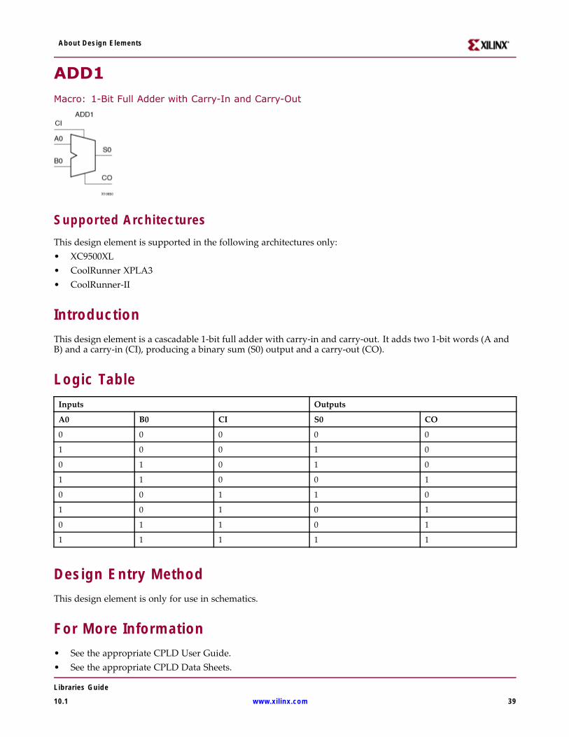
About Design Elements
ADD1Macro: 1-Bit Full Adder with Carry-In and Carry-Out
Supported ArchitecturesThis design element is supported in the following architectures only:• XC9500XL• CoolRunner XPLA3• CoolRunner-II
IntroductionThis design element is a cascadable 1-bit full adder with carry-in and carry-out. It adds two 1-bit words (A andB) and a carry-in (CI), producing a binary sum (S0) output and a carry-out (CO).
Logic TableInputs Outputs
A0 B0 CI S0 CO
0 0 0 0 0
1 0 0 1 0
0 1 0 1 0
1 1 0 0 1
0 0 1 1 0
1 0 1 0 1
0 1 1 0 1
1 1 1 1 1
Design Entry MethodThis design element is only for use in schematics.
For More Information• See the appropriate CPLD User Guide.• See the appropriate CPLD Data Sheets.
Libraries Guide
10.1 www.xilinx.com 39

About Design Elements
ADD16Macro: 16-Bit Cascadable Full Adder with Carry-In, Carry-Out, and Overflow
Supported ArchitecturesThis design element is supported in the following architectures only:• XC9500XL• CoolRunner XPLA3• CoolRunner-II
IntroductionThis design element adds two words and a carry-in (CI), producing a sum output and carry-out (CO) or overflow(OFL). The factors added are A15 – A0, B15 – B0 and CI, producing the sum output S15 – S0 and CO (or OFL).
Logic TableInput Output
A B S
An Bn An+Bn+CI
CI: Value of input CI.
Unsigned Binary Versus Twos ComplementThis design element can operate on either 16-bit unsigned binary numbers or 16-bit twos-complement numbers,respectively. If the inputs are interpreted as unsigned binary, the result can be interpreted as unsigned binary. Ifthe inputs are interpreted as twos complement, the output can be interpreted as twos complement. The onlyfunctional difference between an unsigned binary operation and a twos-complement operation is the way theydetermine when “overflow” occurs. Unsigned binary uses CO, while twos-complement uses OFL to determinewhen “overflow” occurs. To interpret the inputs as unsigned binary, follow the CO output. To interpret theinputs as twos complement, follow the OFL output.
Unsigned Binary OperationFor unsigned binary operation, this element represents numbers between 0 and 65535, inclusive. OFL is ignoredin unsigned binary operation.
Libraries Guide
40 www.xilinx.com 10.1

About Design Elements
Twos-Complement OperationFor twos-complement operation, this element can represent numbers between -32768 and +32767, inclusive. OFLis active (High) when the sum exceeds the bounds of the adder. CO is ignored in twos-complement operation.
Design Entry MethodThis design element is only for use in schematics.
For More Information• See the appropriate CPLD User Guide.
• See the appropriate CPLD Data Sheets.
Libraries Guide
10.1 www.xilinx.com 41

About Design Elements
ADD4
Macro: 4-Bit Cascadable Full Adder with Carry-In, Carry-Out, and Overflow
Supported Architectures
This design element is supported in the following architectures only:
• XC9500XL
• CoolRunner XPLA3
• CoolRunner-II
IntroductionThis design element adds two words and a carry-in (CI), producing a sum output and carry-out (CO) or overflow(OFL). The factors added are A3 – A0, B3 – B0, and CI producing the sum output S3 – S0 and CO (or OFL).
Logic TableInput Output
A B S
An Bn An+Bn+CI
CI: Value of input CI.
Unsigned Binary Versus Twos ComplementThis design element can operate on either 4-bit unsigned binary numbers or 4-bit twos-complement numbers,respectively. If the inputs are interpreted as unsigned binary, the result can be interpreted as unsigned binary. Ifthe inputs are interpreted as twos complement, the output can be interpreted as twos complement. The onlyfunctional difference between an unsigned binary operation and a twos-complement operation is the way theydetermine when “overflow” occurs. Unsigned binary uses CO, while twos-complement uses OFL to determinewhen “overflow” occurs. To interpret the inputs as unsigned binary, follow the CO output. To interpret theinputs as twos complement, follow the OFL output.
Libraries Guide
42 www.xilinx.com 10.1

About Design Elements
Unsigned Binary Operation
For unsigned binary operation, this element represents numbers from 0 to 15, inclusive. OFL is ignoredin unsigned binary operation.
Twos-Complement OperationFor twos-complement operation, this element can represent numbers between -8 and +7, inclusive. OFL is active(High) when the sum exceeds the bounds of the adder. CO is ignored in twos-complement operation.
Design Entry MethodThis design element is only for use in schematics.
For More Information• See the appropriate CPLD User Guide.
• See the appropriate CPLD Data Sheets.
Libraries Guide
10.1 www.xilinx.com 43
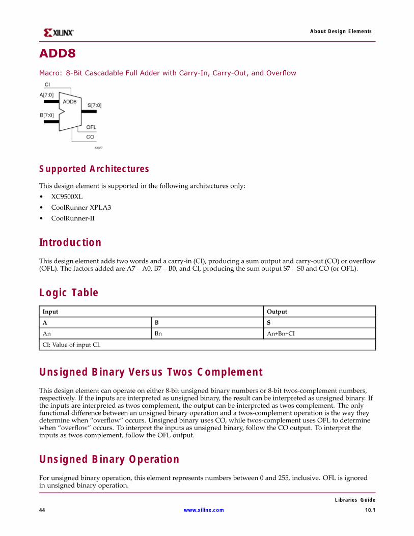
About Design Elements
ADD8
Macro: 8-Bit Cascadable Full Adder with Carry-In, Carry-Out, and Overflow
Supported ArchitecturesThis design element is supported in the following architectures only:• XC9500XL• CoolRunner XPLA3• CoolRunner-II
IntroductionThis design element adds two words and a carry-in (CI), producing a sum output and carry-out (CO) or overflow(OFL). The factors added are A7 – A0, B7 – B0, and CI, producing the sum output S7 – S0 and CO (or OFL).
Logic TableInput Output
A B S
An Bn An+Bn+CI
CI: Value of input CI.
Unsigned Binary Versus Twos ComplementThis design element can operate on either 8-bit unsigned binary numbers or 8-bit twos-complement numbers,respectively. If the inputs are interpreted as unsigned binary, the result can be interpreted as unsigned binary. Ifthe inputs are interpreted as twos complement, the output can be interpreted as twos complement. The onlyfunctional difference between an unsigned binary operation and a twos-complement operation is the way theydetermine when “overflow” occurs. Unsigned binary uses CO, while twos-complement uses OFL to determinewhen “overflow” occurs. To interpret the inputs as unsigned binary, follow the CO output. To interpret theinputs as twos complement, follow the OFL output.
Unsigned Binary OperationFor unsigned binary operation, this element represents numbers between 0 and 255, inclusive. OFL is ignoredin unsigned binary operation.
Libraries Guide
44 www.xilinx.com 10.1

About Design Elements
Twos-Complement OperationFor twos-complement operation, this element can represent numbers between -128 and +127, inclusive. OFL isactive (High) when the sum exceeds the bounds of the adder. CO is ignored in twos-complement operation.
Design Entry MethodThis design element is only for use in schematics.
For More Information• See the appropriate CPLD User Guide.
• See the appropriate CPLD Data Sheets.
Libraries Guide
10.1 www.xilinx.com 45

About Design Elements
ADSU1Macro: 1-Bit Cascadable Adder/Subtracter with Carry-In, Carry-Out
Supported ArchitecturesThis design element is supported in the following architectures only:• XC9500XL• CoolRunner XPLA3• CoolRunner-II
IntroductionWhen the ADD input is High, this element adds two 1-bit words (A0 and B0) with a carry-in (CI), producing a1-bit output (S0) and a carry-out (CO). When the ADD input is Low, B0 is subtracted from A0, producinga result (S0) and borrow (CO).
In add mode, CO represents a carry-out, and CO and CI are active-High. In subtract mode, CO represents aborrow, and CO and CI are active-Low.
Add Function, ADD=1
Inputs Outputs
A0 B0 CI S0 CO
0 0 0 0 0
0 1 0 1 0
1 0 0 1 0
1 1 0 0 1
0 0 1 1 0
0 1 1 0 1
1 0 1 0 1
1 1 1 1 1
Subtract Function, ADD=0
Inputs Outputs
A0 B0 CI S0 CO
0 0 0 1 0
0 1 0 0 0
1 0 0 0 1
Libraries Guide
46 www.xilinx.com 10.1
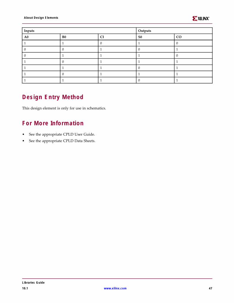
About Design Elements
Inputs Outputs
A0 B0 CI S0 CO
1 1 0 1 0
0 0 1 0 1
0 1 1 1 0
1 0 1 1 1
1 1 1 0 1
1 0 1 1 1
1 1 1 0 1
Design Entry MethodThis design element is only for use in schematics.
For More Information• See the appropriate CPLD User Guide.
• See the appropriate CPLD Data Sheets.
Libraries Guide
10.1 www.xilinx.com 47

About Design Elements
ADSU16
Macro: 16-Bit Cascadable Adder/Subtracter with Carry-In, Carry-Out, and Overflow
Supported ArchitecturesThis design element is supported in the following architectures only:• XC9500XL• CoolRunner XPLA3• CoolRunner-II
IntroductionWhen the ADD input is High, this element adds two 16-bit words (A15 – A0 and B15 – B0) and a carry-in (CI),producing a 16-bit sum output (S15 – S0) and carry-out (CO) or overflow (OFL).
When the ADD input is Low, this element subtracts B15 – B0 from A15– A0, producing a difference output anda carry-out (CO) or an overflow (OFL).
In add mode, CO and CI are active-High. In subtract mode, CO and CI are active-Low. OFL is active-High inadd and subtract modes.
Logic TableInput Output
ADD A B S
1 An Bn An+Bn+CI*
0 An Bn An-Bn-CI*
CI*: ADD = 0, CI, CO active LOW
CI*: ADD = 1, CI, CO active HIGH
Unsigned Binary Versus Twos Complement
This design element can operate on either 16-bit unsigned binary numbers or 16-bit twos-complement numbers.If the inputs are interpreted as unsigned binary, the result can be interpreted as unsigned binary. If the inputsare interpreted as twos complement, the output can be interpreted as twos complement. The only functionaldifference between an unsigned binary operation and a twos-complement operation is the way they determinewhen “overflow” occurs. Unsigned binary uses CO, while twos complement uses OFL to determine when“overflow” occurs.
Libraries Guide
48 www.xilinx.com 10.1

About Design Elements
With adder/subtracters, either unsigned binary or twos-complement operations cause an overflow. If the resultcrosses the overflow boundary, an overflow is generated. Similarly, when the result crosses the carry-outboundary, a carry-out is generated.
Unsigned Binary Operation
For unsigned binary operation, this element can represent numbers between 0 and 65535, inclusive. In addmode, CO is active (High) when the sum exceeds the bounds of the adder/subtracter. In subtract mode, CO is anactive-Low borrow-out and goes Low when the difference exceeds the bounds.
An unsigned binary “overflow” that is always active-High can be generated by gating the ADD signal and COas follows:unsigned overflow = CO XOR ADD
OFL is ignored in unsigned binary operation.
Twos-Complement Operation
For twos-complement operation, this element can represent numbers between -32768 and +32767, inclusive.
If an addition or subtraction operation result exceeds this range, the OFL output goes High. CO is ignoredin twos-complement operation.
Design Entry MethodThis design element is only for use in schematics.
For More Information• See the appropriate CPLD User Guide.
• See the appropriate CPLD Data Sheets.
Libraries Guide
10.1 www.xilinx.com 49

About Design Elements
ADSU4
Macro: 4-Bit Cascadable Adder/Subtracter with Carry-In, Carry-Out, and Overflow
Supported Architectures
This design element is supported in the following architectures only:
• XC9500XL
• CoolRunner XPLA3
• CoolRunner-II
IntroductionWhen the ADD input is High, this element adds two 4-bit words (A3 – A0 and B3 – B0) and a carry-in (CI),producing a 4-bit sum output (S3 – S0) and a carry-out (CO) or an overflow (OFL).
When the ADD input is Low, this element subtracts B3 – B0 from A3– A0, producing a 4-bit difference output(S3 – S0) and a carry-out (CO) or an overflow (OFL).
In add mode, CO and CI are active-High. In subtract mode, CO and CI are active-Low. OFL is active-High inadd and subtract modes.
Logic TableInput Output
ADD A B S
1 An Bn An+Bn+CI*
0 An Bn An-Bn-CI*
CI*: ADD = 0, CI, CO active LOW
CI*: ADD = 1, CI, CO active HIGH
Libraries Guide
50 www.xilinx.com 10.1

About Design Elements
Unsigned Binary Versus Twos Complement
This design element can operate on either 4-bit unsigned binary numbers or 4-bit twos-complement numbers. Ifthe inputs are interpreted as unsigned binary, the result can be interpreted as unsigned binary. If the inputsare interpreted as twos complement, the output can be interpreted as twos complement. The only functionaldifference between an unsigned binary operation and a twos-complement operation is the way they determinewhen “overflow” occurs. Unsigned binary uses CO, while twos complement uses OFL to determine when“overflow” occurs.
With adder/subtracters, either unsigned binary or twos-complement operations cause an overflow. If the resultcrosses the overflow boundary, an overflow is generated. Similarly, when the result crosses the carry-outboundary, a carry-out is generated.
Unsigned Binary Operation
For unsigned binary operation, ADSU4 can represent numbers between 0 and 15, inclusive. In add mode, CO isactive (High) when the sum exceeds the bounds of the adder/subtracter. In subtract mode, CO is an active-Lowborrow-out and goes Low when the difference exceeds the bounds.
An unsigned binary “overflow” that is always active-High can be generated by gating the ADD signal and COas follows:unsigned overflow = CO XOR ADD
OFL is ignored in unsigned binary operation.
Twos-Complement Operation
For twos-complement operation, this element can represent numbers between -8 and +7, inclusive.
If an addition or subtraction operation result exceeds this range, the OFL output goes High. CO is ignoredin twos-complement operation.
Design Entry MethodThis design element is only for use in schematics.
For More Information• See the appropriate CPLD User Guide.
• See the appropriate CPLD Data Sheets.
Libraries Guide
10.1 www.xilinx.com 51

About Design Elements
ADSU8
Macro: 8-Bit Cascadable Adder/Subtracter with Carry-In, Carry-Out, and Overflow
Supported ArchitecturesThis design element is supported in the following architectures only:• XC9500XL• CoolRunner XPLA3• CoolRunner-II
IntroductionWhen the ADD input is High, this element adds two 8-bit words (A7 – A0 and B7 – B0) and a carry-in (CI),producing, an 8-bit sum output (S7 – S0) and carry-out (CO) or an overflow (OFL).
When the ADD input is Low, this element subtracts B7 – B0 from A7 – A0, producing an 8-bit difference output(S7 – S0) and a carry-out (CO) or an overflow (OFL).
In add mode, CO and CI are active-High. In subtract mode, CO and CI are active-Low. OFL is active-High inadd and subtract modes.
Logic TableInput Output
ADD A B S
1 An Bn An+Bn+CI*
0 An Bn An-Bn-CI*
CI*: ADD = 0, CI, CO active LOW
CI*: ADD = 1, CI, CO active HIGH
Unsigned Binary Versus Twos Complement
This design element can operate on either 8-bit unsigned binary numbers or 8-bit twos-complement numbers. Ifthe inputs are interpreted as unsigned binary, the result can be interpreted as unsigned binary. If the inputsare interpreted as twos complement, the output can be interpreted as twos complement. The only functionaldifference between an unsigned binary operation and a twos-complement operation is the way they determinewhen “overflow” occurs. Unsigned binary uses CO, while twos complement uses OFL to determine when“overflow” occurs.
Libraries Guide
52 www.xilinx.com 10.1

About Design Elements
With adder/subtracters, either unsigned binary or twos-complement operations cause an overflow. If the resultcrosses the overflow boundary, an overflow is generated. Similarly, when the result crosses the carry-outboundary, a carry-out is generated.
Unsigned Binary Operation
For unsigned binary operation, this element can represent numbers between 0 and 255, inclusive. In add mode,CO is active (High) when the sum exceeds the bounds of the adder/subtracter. In subtract mode, CO is anactive-Low borrow-out and goes Low when the difference exceeds the bounds.
An unsigned binary “overflow” that is always active-High can be generated by gating the ADD signal and COas follows:unsigned overflow = CO XOR ADD
OFL is ignored in unsigned binary operation.
Twos-Complement Operation
For twos-complement operation, this element can represent numbers between -128 and +127, inclusive.
If an addition or subtraction operation result exceeds this range, the OFL output goes High. CO is ignoredin twos-complement operation.
Design Entry MethodThis design element is only for use in schematics.
For More Information• See the appropriate CPLD User Guide.
• See the appropriate CPLD Data Sheets.
Libraries Guide
10.1 www.xilinx.com 53
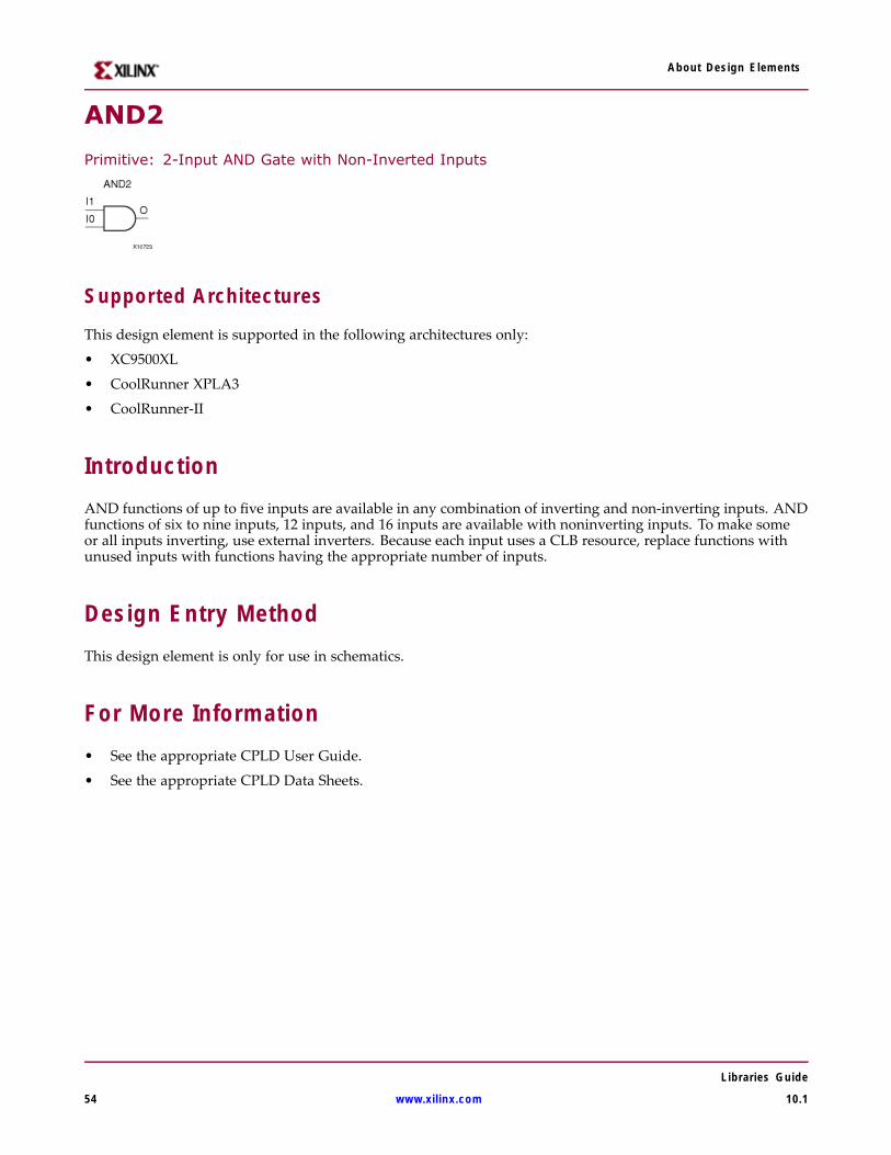
About Design Elements
AND2
Primitive: 2-Input AND Gate with Non-Inverted Inputs
Supported Architectures
This design element is supported in the following architectures only:
• XC9500XL
• CoolRunner XPLA3
• CoolRunner-II
IntroductionAND functions of up to five inputs are available in any combination of inverting and non-inverting inputs. ANDfunctions of six to nine inputs, 12 inputs, and 16 inputs are available with noninverting inputs. To make someor all inputs inverting, use external inverters. Because each input uses a CLB resource, replace functions withunused inputs with functions having the appropriate number of inputs.
Design Entry MethodThis design element is only for use in schematics.
For More Information• See the appropriate CPLD User Guide.
• See the appropriate CPLD Data Sheets.
Libraries Guide
54 www.xilinx.com 10.1
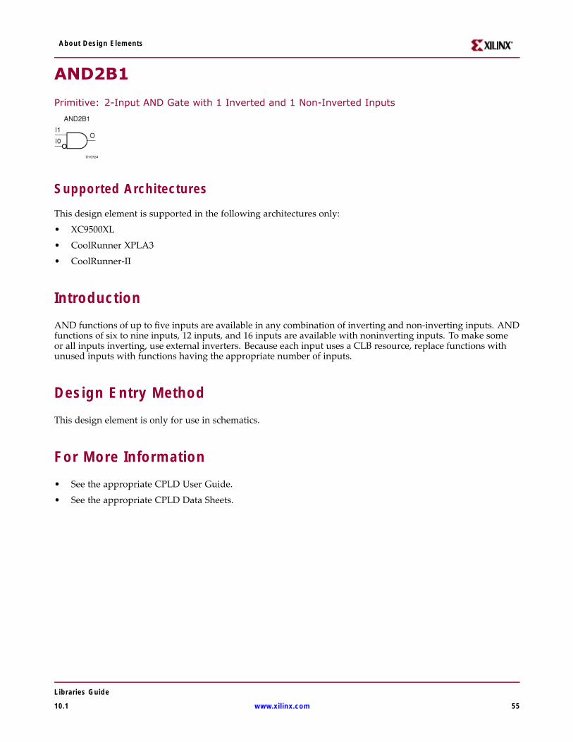
About Design Elements
AND2B1
Primitive: 2-Input AND Gate with 1 Inverted and 1 Non-Inverted Inputs
Supported Architectures
This design element is supported in the following architectures only:
• XC9500XL
• CoolRunner XPLA3
• CoolRunner-II
IntroductionAND functions of up to five inputs are available in any combination of inverting and non-inverting inputs. ANDfunctions of six to nine inputs, 12 inputs, and 16 inputs are available with noninverting inputs. To make someor all inputs inverting, use external inverters. Because each input uses a CLB resource, replace functions withunused inputs with functions having the appropriate number of inputs.
Design Entry MethodThis design element is only for use in schematics.
For More Information• See the appropriate CPLD User Guide.
• See the appropriate CPLD Data Sheets.
Libraries Guide
10.1 www.xilinx.com 55

About Design Elements
AND2B2
Primitive: 2-Input AND Gate with Inverted Inputs
Supported Architectures
This design element is supported in the following architectures only:
• XC9500XL
• CoolRunner XPLA3
• CoolRunner-II
IntroductionAND functions of up to five inputs are available in any combination of inverting and non-inverting inputs. ANDfunctions of six to nine inputs, 12 inputs, and 16 inputs are available with noninverting inputs. To make someor all inputs inverting, use external inverters. Because each input uses a CLB resource, replace functions withunused inputs with functions having the appropriate number of inputs.
Design Entry MethodThis design element is only for use in schematics.
For More Information• See the appropriate CPLD User Guide.
• See the appropriate CPLD Data Sheets.
Libraries Guide
56 www.xilinx.com 10.1

About Design Elements
AND3
Primitive: 3-Input AND Gate with Non-Inverted Inputs
Supported Architectures
This design element is supported in the following architectures only:
• XC9500XL
• CoolRunner XPLA3
• CoolRunner-II
IntroductionAND functions of up to five inputs are available in any combination of inverting and non-inverting inputs. ANDfunctions of six to nine inputs, 12 inputs, and 16 inputs are available with noninverting inputs. To make someor all inputs inverting, use external inverters. Because each input uses a CLB resource, replace functions withunused inputs with functions having the appropriate number of inputs.
Design Entry MethodThis design element is only for use in schematics.
For More Information• See the appropriate CPLD User Guide.
• See the appropriate CPLD Data Sheets.
Libraries Guide
10.1 www.xilinx.com 57

About Design Elements
AND3B1
Primitive: 3-Input AND Gate with 1 Inverted and 2 Non-Inverted Inputs
Supported Architectures
This design element is supported in the following architectures only:
• XC9500XL
• CoolRunner XPLA3
• CoolRunner-II
IntroductionAND functions of up to five inputs are available in any combination of inverting and non-inverting inputs. ANDfunctions of six to nine inputs, 12 inputs, and 16 inputs are available with noninverting inputs. To make someor all inputs inverting, use external inverters. Because each input uses a CLB resource, replace functions withunused inputs with functions having the appropriate number of inputs.
Design Entry MethodThis design element is only for use in schematics.
For More Information• See the appropriate CPLD User Guide.
• See the appropriate CPLD Data Sheets.
Libraries Guide
58 www.xilinx.com 10.1

About Design Elements
AND3B2
Primitive: 3-Input AND Gate with 2 Inverted and 1 Non-Inverted Inputs
Supported Architectures
This design element is supported in the following architectures only:
• XC9500XL
• CoolRunner XPLA3
• CoolRunner-II
IntroductionAND functions of up to five inputs are available in any combination of inverting and non-inverting inputs. ANDfunctions of six to nine inputs, 12 inputs, and 16 inputs are available with noninverting inputs. To make someor all inputs inverting, use external inverters. Because each input uses a CLB resource, replace functions withunused inputs with functions having the appropriate number of inputs.
Design Entry MethodThis design element is only for use in schematics.
For More Information• See the appropriate CPLD User Guide.
• See the appropriate CPLD Data Sheets.
Libraries Guide
10.1 www.xilinx.com 59

About Design Elements
AND3B3
Primitive: 3-Input AND Gate with Inverted Inputs
Supported Architectures
This design element is supported in the following architectures only:
• XC9500XL
• CoolRunner XPLA3
• CoolRunner-II
IntroductionAND functions of up to five inputs are available in any combination of inverting and non-inverting inputs. ANDfunctions of six to nine inputs, 12 inputs, and 16 inputs are available with noninverting inputs. To make someor all inputs inverting, use external inverters. Because each input uses a CLB resource, replace functions withunused inputs with functions having the appropriate number of inputs.
Design Entry MethodThis design element is only for use in schematics.
For More Information• See the appropriate CPLD User Guide.
• See the appropriate CPLD Data Sheets.
Libraries Guide
60 www.xilinx.com 10.1

About Design Elements
AND4
Primitive: 4-Input AND Gate with Non-Inverted Inputs
Supported Architectures
This design element is supported in the following architectures only:
• XC9500XL
• CoolRunner XPLA3
• CoolRunner-II
IntroductionAND functions of up to five inputs are available in any combination of inverting and non-inverting inputs. ANDfunctions of six to nine inputs, 12 inputs, and 16 inputs are available with noninverting inputs. To make someor all inputs inverting, use external inverters. Because each input uses a CLB resource, replace functions withunused inputs with functions having the appropriate number of inputs.
Design Entry MethodThis design element is only for use in schematics.
For More Information• See the appropriate CPLD User Guide.
• See the appropriate CPLD Data Sheets.
Libraries Guide
10.1 www.xilinx.com 61
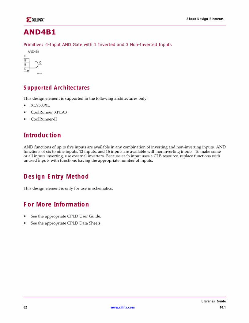
About Design Elements
AND4B1
Primitive: 4-Input AND Gate with 1 Inverted and 3 Non-Inverted Inputs
Supported Architectures
This design element is supported in the following architectures only:
• XC9500XL
• CoolRunner XPLA3
• CoolRunner-II
IntroductionAND functions of up to five inputs are available in any combination of inverting and non-inverting inputs. ANDfunctions of six to nine inputs, 12 inputs, and 16 inputs are available with noninverting inputs. To make someor all inputs inverting, use external inverters. Because each input uses a CLB resource, replace functions withunused inputs with functions having the appropriate number of inputs.
Design Entry MethodThis design element is only for use in schematics.
For More Information• See the appropriate CPLD User Guide.
• See the appropriate CPLD Data Sheets.
Libraries Guide
62 www.xilinx.com 10.1

About Design Elements
AND4B2
Primitive: 4-Input AND Gate with 2 Inverted and 2 Non-Inverted Inputs
Supported Architectures
This design element is supported in the following architectures only:
• XC9500XL
• CoolRunner XPLA3
• CoolRunner-II
IntroductionAND functions of up to five inputs are available in any combination of inverting and non-inverting inputs. ANDfunctions of six to nine inputs, 12 inputs, and 16 inputs are available with noninverting inputs. To make someor all inputs inverting, use external inverters. Because each input uses a CLB resource, replace functions withunused inputs with functions having the appropriate number of inputs.
Design Entry MethodThis design element is only for use in schematics.
For More Information• See the appropriate CPLD User Guide.
• See the appropriate CPLD Data Sheets.
Libraries Guide
10.1 www.xilinx.com 63

About Design Elements
AND4B3
Primitive: 4-Input AND Gate with 3 Inverted and 1 Non-Inverted Inputs
Supported Architectures
This design element is supported in the following architectures only:
• XC9500XL
• CoolRunner XPLA3
• CoolRunner-II
IntroductionAND functions of up to five inputs are available in any combination of inverting and non-inverting inputs. ANDfunctions of six to nine inputs, 12 inputs, and 16 inputs are available with noninverting inputs. To make someor all inputs inverting, use external inverters. Because each input uses a CLB resource, replace functions withunused inputs with functions having the appropriate number of inputs.
Design Entry MethodThis design element is only for use in schematics.
For More Information• See the appropriate CPLD User Guide.
• See the appropriate CPLD Data Sheets.
Libraries Guide
64 www.xilinx.com 10.1

About Design Elements
AND4B4
Primitive: 4-Input AND Gate with Inverted Inputs
Supported Architectures
This design element is supported in the following architectures only:
• XC9500XL
• CoolRunner XPLA3
• CoolRunner-II
IntroductionAND functions of up to five inputs are available in any combination of inverting and non-inverting inputs. ANDfunctions of six to nine inputs, 12 inputs, and 16 inputs are available with noninverting inputs. To make someor all inputs inverting, use external inverters. Because each input uses a CLB resource, replace functions withunused inputs with functions having the appropriate number of inputs.
Design Entry MethodThis design element is only for use in schematics.
For More Information• See the appropriate CPLD User Guide.
• See the appropriate CPLD Data Sheets.
Libraries Guide
10.1 www.xilinx.com 65

About Design Elements
AND5
Primitive: 5-Input AND Gate with Non-Inverted Inputs
Supported Architectures
This design element is supported in the following architectures only:
• XC9500XL
• CoolRunner XPLA3
• CoolRunner-II
IntroductionAND functions of up to five inputs are available in any combination of inverting and non-inverting inputs. ANDfunctions of six to nine inputs, 12 inputs, and 16 inputs are available with noninverting inputs. To make someor all inputs inverting, use external inverters. Because each input uses a CLB resource, replace functions withunused inputs with functions having the appropriate number of inputs.
Design Entry MethodThis design element is only for use in schematics.
For More Information• See the appropriate CPLD User Guide.
• See the appropriate CPLD Data Sheets.
Libraries Guide
66 www.xilinx.com 10.1

About Design Elements
AND5B1
Primitive: 5-Input AND Gate with 1 Inverted and 4 Non-Inverted Inputs
Supported Architectures
This design element is supported in the following architectures only:
• XC9500XL
• CoolRunner XPLA3
• CoolRunner-II
IntroductionAND functions of up to five inputs are available in any combination of inverting and non-inverting inputs. ANDfunctions of six to nine inputs, 12 inputs, and 16 inputs are available with noninverting inputs. To make someor all inputs inverting, use external inverters. Because each input uses a CLB resource, replace functions withunused inputs with functions having the appropriate number of inputs.
Design Entry MethodThis design element is only for use in schematics.
For More Information• See the appropriate CPLD User Guide.
• See the appropriate CPLD Data Sheets.
Libraries Guide
10.1 www.xilinx.com 67

About Design Elements
AND5B2
Primitive: 5-Input AND Gate with 2 Inverted and 3 Non-Inverted Inputs
Supported Architectures
This design element is supported in the following architectures only:
• XC9500XL
• CoolRunner XPLA3
• CoolRunner-II
IntroductionAND functions of up to five inputs are available in any combination of inverting and non-inverting inputs. ANDfunctions of six to nine inputs, 12 inputs, and 16 inputs are available with noninverting inputs. To make someor all inputs inverting, use external inverters. Because each input uses a CLB resource, replace functions withunused inputs with functions having the appropriate number of inputs.
Design Entry MethodThis design element is only for use in schematics.
For More Information• See the appropriate CPLD User Guide.
• See the appropriate CPLD Data Sheets.
Libraries Guide
68 www.xilinx.com 10.1

About Design Elements
AND5B3
Primitive: 5-Input AND Gate with 3 Inverted and 2 Non-Inverted Inputs
Supported Architectures
This design element is supported in the following architectures only:
• XC9500XL
• CoolRunner XPLA3
• CoolRunner-II
IntroductionAND functions of up to five inputs are available in any combination of inverting and non-inverting inputs. ANDfunctions of six to nine inputs, 12 inputs, and 16 inputs are available with noninverting inputs. To make someor all inputs inverting, use external inverters. Because each input uses a CLB resource, replace functions withunused inputs with functions having the appropriate number of inputs.
Design Entry MethodThis design element is only for use in schematics.
For More Information• See the appropriate CPLD User Guide.
• See the appropriate CPLD Data Sheets.
Libraries Guide
10.1 www.xilinx.com 69

About Design Elements
AND5B4
Primitive: 5-Input AND Gate with 4 Inverted and 1 Non-Inverted Inputs
Supported Architectures
This design element is supported in the following architectures only:
• XC9500XL
• CoolRunner XPLA3
• CoolRunner-II
IntroductionAND functions of up to five inputs are available in any combination of inverting and non-inverting inputs. ANDfunctions of six to nine inputs, 12 inputs, and 16 inputs are available with noninverting inputs. To make someor all inputs inverting, use external inverters. Because each input uses a CLB resource, replace functions withunused inputs with functions having the appropriate number of inputs.
Design Entry MethodThis design element is only for use in schematics.
For More Information• See the appropriate CPLD User Guide.
• See the appropriate CPLD Data Sheets.
Libraries Guide
70 www.xilinx.com 10.1

About Design Elements
AND5B5
Primitive: 5-Input AND Gate with Inverted Inputs
Supported Architectures
This design element is supported in the following architectures only:
• XC9500XL
• CoolRunner XPLA3
• CoolRunner-II
IntroductionAND functions of up to five inputs are available in any combination of inverting and non-inverting inputs. ANDfunctions of six to nine inputs, 12 inputs, and 16 inputs are available with noninverting inputs. To make someor all inputs inverting, use external inverters. Because each input uses a CLB resource, replace functions withunused inputs with functions having the appropriate number of inputs.
Design Entry MethodThis design element is only for use in schematics.
For More Information• See the appropriate CPLD User Guide.
• See the appropriate CPLD Data Sheets.
Libraries Guide
10.1 www.xilinx.com 71

About Design Elements
AND6
Macro: 6-Input AND Gate with Non-Inverted Inputs
Supported Architectures
This design element is supported in the following architectures only:
• XC9500XL
• CoolRunner XPLA3
• CoolRunner-II
IntroductionAND functions of up to five inputs are available in any combination of inverting and non-inverting inputs. ANDfunctions of six to nine inputs, 12 inputs, and 16 inputs are available with noninverting inputs. To make someor all inputs inverting, use external inverters. Because each input uses a CLB resource, replace functions withunused inputs with functions having the appropriate number of inputs.
Design Entry MethodThis design element is only for use in schematics.
For More Information• See the appropriate CPLD User Guide.
• See the appropriate CPLD Data Sheets.
Libraries Guide
72 www.xilinx.com 10.1

About Design Elements
AND7
Macro: 7-Input AND Gate with Non-Inverted Inputs
Supported Architectures
This design element is supported in the following architectures only:
• XC9500XL
• CoolRunner XPLA3
• CoolRunner-II
IntroductionAND functions of up to five inputs are available in any combination of inverting and non-inverting inputs. ANDfunctions of six to nine inputs, 12 inputs, and 16 inputs are available with noninverting inputs. To make someor all inputs inverting, use external inverters. Because each input uses a CLB resource, replace functions withunused inputs with functions having the appropriate number of inputs.
Design Entry MethodThis design element is only for use in schematics.
For More Information• See the appropriate CPLD User Guide.
• See the appropriate CPLD Data Sheets.
Libraries Guide
10.1 www.xilinx.com 73
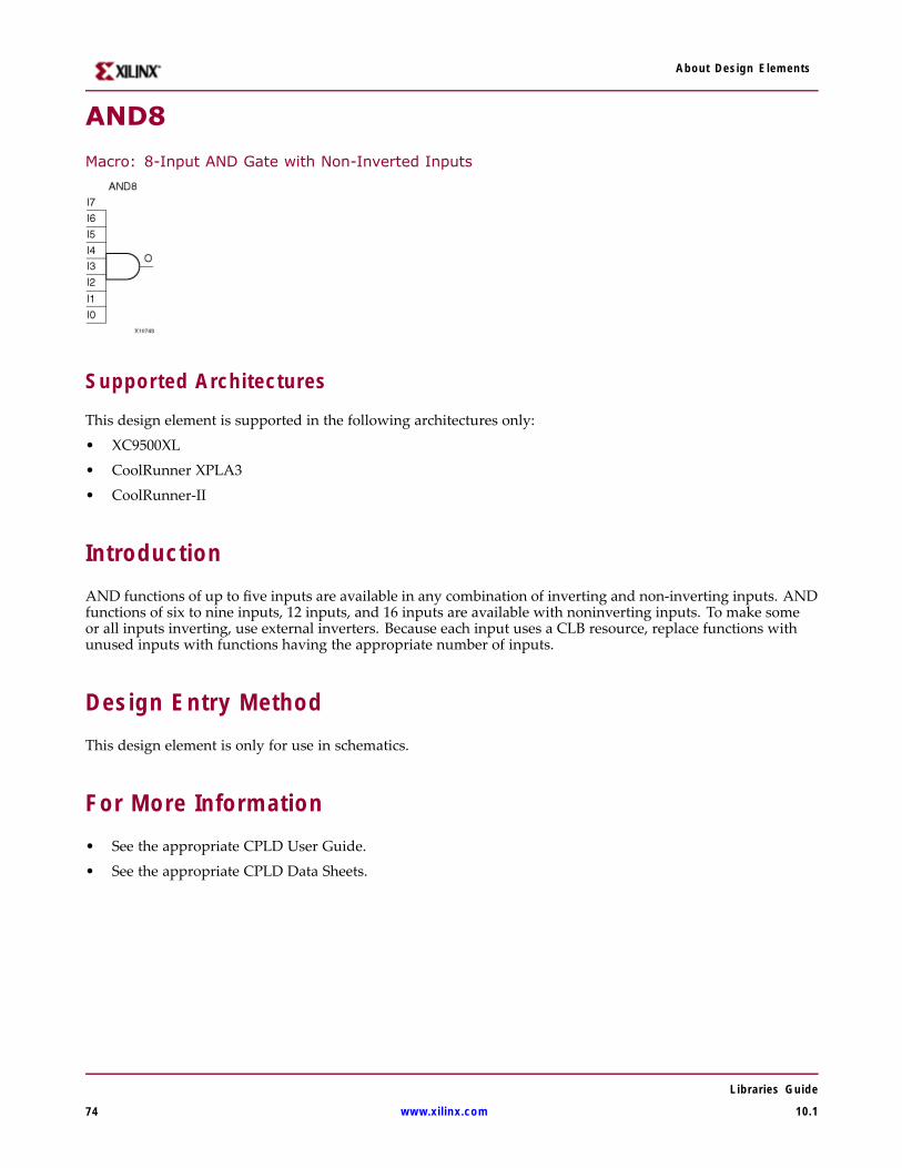
About Design Elements
AND8
Macro: 8-Input AND Gate with Non-Inverted Inputs
Supported Architectures
This design element is supported in the following architectures only:
• XC9500XL
• CoolRunner XPLA3
• CoolRunner-II
IntroductionAND functions of up to five inputs are available in any combination of inverting and non-inverting inputs. ANDfunctions of six to nine inputs, 12 inputs, and 16 inputs are available with noninverting inputs. To make someor all inputs inverting, use external inverters. Because each input uses a CLB resource, replace functions withunused inputs with functions having the appropriate number of inputs.
Design Entry MethodThis design element is only for use in schematics.
For More Information• See the appropriate CPLD User Guide.
• See the appropriate CPLD Data Sheets.
Libraries Guide
74 www.xilinx.com 10.1

About Design Elements
AND9
Macro: 9-Input AND Gate with Non-Inverted Inputs
Supported Architectures
This design element is supported in the following architectures only:
• XC9500XL
• CoolRunner XPLA3
• CoolRunner-II
IntroductionAND functions of up to five inputs are available in any combination of inverting and non-inverting inputs. ANDfunctions of six to nine inputs, 12 inputs, and 16 inputs are available with noninverting inputs. To make someor all inputs inverting, use external inverters. Because each input uses a CLB resource, replace functions withunused inputs with functions having the appropriate number of inputs.
Design Entry MethodThis design element is only for use in schematics.
For More Information• See the appropriate CPLD User Guide.
• See the appropriate CPLD Data Sheets.
Libraries Guide
10.1 www.xilinx.com 75

About Design Elements
BRLSHFT4Macro: 4-Bit Barrel Shifter
Supported ArchitecturesThis design element is supported in the following architectures only:• XC9500XL• CoolRunner XPLA3• CoolRunner-II
IntroductionThis design element is a 4-bit barrel shifter that can rotate four inputs (I3 – I0) up to four places. The controlinputs (S1 and S0) determine the number of positions, from one to four, that the data is rotated. The four outputs(O3 – O0) reflect the shifted data inputs.
Logic TableInputs Outputs
S1 S0 I0 I1 I2 I3 O0 O1 O2 O3
0 0 a b c d a b c d
0 1 a b c d b c d a
1 0 a b c d c d a b
1 1 a b c d d a b c
Design Entry MethodThis design element is only for use in schematics.
For More Information• See the appropriate CPLD User Guide.• See the appropriate CPLD Data Sheets.
Libraries Guide
76 www.xilinx.com 10.1

About Design Elements
BRLSHFT8
Macro: 8-Bit Barrel Shifter
Supported ArchitecturesThis design element is supported in the following architectures only:• XC9500XL• CoolRunner XPLA3• CoolRunner-II
IntroductionThis design element is an 8-bit barrel shifter, can rotate the eight inputs (I7 – I0) up to eight places. The controlinputs (S2 – S0) determine the number of positions, from one to eight, that the data is rotated. The eight outputs(O7 – O0) reflect the shifted data inputs.
Logic TableInputs Outputs
S2 S1 S0 I0 I1 I2 I3 I4 I5 I6 I7 O0 O1 O2 O3 O4 O5 O6 O7
0 0 0 a b c d e f g h a b c d e f g h
0 0 1 a b c d e f g h b c d e f g h a
0 1 0 a b c d e f g h c d e f g h a b
0 1 1 a b c d e f g h d e f g h a b c
1 0 0 a b c d e f g h e f g h a b c d
1 0 1 a b c d e f g h f g h a b c d e
1 1 0 a b c d e f g h g h a b c d e f
1 1 1 a b c d e f g h h a b c d e f g
Libraries Guide
10.1 www.xilinx.com 77

About Design Elements
Design Entry MethodThis design element is only for use in schematics.
For More Information• See the appropriate CPLD User Guide.
• See the appropriate CPLD Data Sheets.
Libraries Guide
78 www.xilinx.com 10.1

About Design Elements
BUF
Primitive: General Purpose Buffer
Supported Architectures
This design element is supported in the following architectures only:
• XC9500XL
• CoolRunner XPLA3
• CoolRunner-II
IntroductionThis is a general-purpose, non-inverting buffer.
This element is not necessary and is removed by the partitioning software (MAP).
Design Entry MethodThis design element is only for use in schematics.
For More Information• See the appropriate CPLD User Guide.
• See the appropriate CPLD Data Sheets.
Libraries Guide
10.1 www.xilinx.com 79

About Design Elements
BUF16
Macro: 16-Bit General Purpose Buffer
Supported Architectures
This design element is supported in the following architectures only:
• XC9500XL
• CoolRunner XPLA3
• CoolRunner-II
IntroductionThis is a 16-bit, general purpose, non-inverting buffer. In working with CPLDs, this element is usuallyremoved, unless you inhibit optimization by applying the OPT=OFF attribute to the symbol, or by using theLOGIC_OPT=OFF global attribute.
Design Entry MethodThis design element is only for use in schematics.
For More Information• See the appropriate CPLD User Guide.
• See the appropriate CPLD Data Sheets.
Libraries Guide
80 www.xilinx.com 10.1

About Design Elements
BUF4
Macro: 4-Bit General Purpose Buffer
Supported Architectures
This design element is supported in the following architectures only:
• XC9500XL
• CoolRunner XPLA3
• CoolRunner-II
IntroductionThis is a 4-bit, general purpose, non-inverting buffer. In working with CPLDs, this element is usuallyremoved, unless you inhibit optimization by applying the OPT=OFF attribute to the symbol, or by using theLOGIC_OPT=OFF global attribute.
Design Entry MethodThis design element is only for use in schematics.
For More Information• See the appropriate CPLD User Guide.
• See the appropriate CPLD Data Sheets.
Libraries Guide
10.1 www.xilinx.com 81

About Design Elements
BUF8
Macro: 8-Bit General Purpose Buffer
Supported Architectures
This design element is supported in the following architectures only:
• XC9500XL
• CoolRunner XPLA3
• CoolRunner-II
IntroductionThis is a 8-bit, general purpose, non-inverting buffer. In working with CPLDs, this element is usuallyremoved, unless you inhibit optimization by applying the OPT=OFF attribute to the symbol, or by using theLOGIC_OPT=OFF global attribute.
Design Entry MethodThis design element is only for use in schematics.
For More Information• See the appropriate CPLD User Guide.
• See the appropriate CPLD Data Sheets.
Libraries Guide
82 www.xilinx.com 10.1

About Design Elements
BUFEPrimitive: Internal 3-State Buffer with Active High Enable
Supported ArchitecturesThis design element is supported in the following architectures only:• XC9500XL• CoolRunner XPLA3
IntroductionThis design element is a single, 3-state buffer with input I and output O, and an active-High output enable (E).When E is High, data on the input of the buffer is transferred to the corresponding output. When E is Low, theoutput is high impedance (Z state or Off). The outputs of the buffers are connected to horizontal longlinesin FPGA architectures.
The outputs of separate symbols for this entity can be tied together to form a bus or a multiplexer. Make surethat only one E is High at any one time. If none of the E inputs is active-High, a “weak-keeper” circuit keepsthe output bus from floating but does not guarantee that the bus remains at the last value driven onto it. Forcertain CPLD devices, output from nets assume the High logic level when all connected BUFE/BUFT buffersare disabled. For FPGA devices, elements need a PULLUP element connected to their output. NGDBuildinserts a PULLUP element if one is not connected.
Logic TableInputs Outputs
E I O
0 X Z
1 1 1
1 0 0
Design Entry MethodThis design element is only for use in schematics.
For More Information• See the appropriate CPLD User Guide.• See the appropriate CPLD Data Sheets.
Libraries Guide
10.1 www.xilinx.com 83
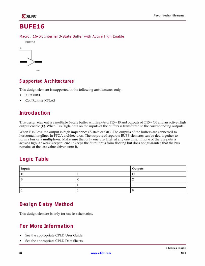
About Design Elements
BUFE16
Macro: 16-Bit Internal 3-State Buffer with Active High Enable
Supported ArchitecturesThis design element is supported in the following architectures only:• XC9500XL• CoolRunner XPLA3
IntroductionThis design element is a multiple 3-state buffer with inputs of I15 – I0 and outputs of O15 – O0 and an active-Highoutput enable (E). When E is High, data on the inputs of the buffers is transferred to the corresponding outputs.
When E is Low, the output is high impedance (Z state or Off). The outputs of the buffers are connected tohorizontal longlines in FPGA architectures. The outputs of separate BUFE elements can be tied together toform a bus or a multiplexer. Make sure that only one E is High at any one time. If none of the E inputs isactive-High, a “weak-keeper” circuit keeps the output bus from floating but does not guarantee that the busremains at the last value driven onto it.
Logic TableInputs Outputs
E I O
0 X Z
1 1 1
1 0 0
Design Entry MethodThis design element is only for use in schematics.
For More Information• See the appropriate CPLD User Guide.• See the appropriate CPLD Data Sheets.
Libraries Guide
84 www.xilinx.com 10.1
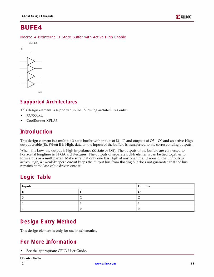
About Design Elements
BUFE4Macro: 4-BitInternal 3-State Buffer with Active High Enable
Supported ArchitecturesThis design element is supported in the following architectures only:• XC9500XL• CoolRunner XPLA3
IntroductionThis design element is a multiple 3-state buffer with inputs of I3 – I0 and outputs of O3 – O0 and an active-Highoutput enable (E). When E is High, data on the inputs of the buffers is transferred to the corresponding outputs.
When E is Low, the output is high impedance (Z state or Off). The outputs of the buffers are connected tohorizontal longlines in FPGA architectures. The outputs of separate BUFE elements can be tied together toform a bus or a multiplexer. Make sure that only one E is High at any one time. If none of the E inputs isactive-High, a “weak-keeper” circuit keeps the output bus from floating but does not guarantee that the busremains at the last value driven onto it.
Logic TableInputs Outputs
E I O
0 X Z
1 1 1
1 0 0
Design Entry MethodThis design element is only for use in schematics.
For More Information• See the appropriate CPLD User Guide.
Libraries Guide
10.1 www.xilinx.com 85

About Design Elements
• See the appropriate CPLD Data Sheets.
Libraries Guide
86 www.xilinx.com 10.1

About Design Elements
BUFE8
Macro: 8-Bit Internal 3-State Buffer with Active High Enable
Supported ArchitecturesThis design element is supported in the following architectures only:• XC9500XL• CoolRunner XPLA3
IntroductionThis design element is a multiple 3-state buffer with inputs of I7 – I0 and outputs of O7 – O0 and an active-Highoutput enable (E). When E is High, data on the inputs of the buffers is transferred to the corresponding outputs.
When E is Low, the output is high impedance (Z state or Off). The outputs of the buffers are connected tohorizontal longlines in FPGA architectures. The outputs of separate BUFE elements can be tied together toform a bus or a multiplexer. Make sure that only one E is High at any one time. If none of the E inputs isactive-High, a “weak-keeper” circuit keeps the output bus from floating but does not guarantee that the busremains at the last value driven onto it.
Logic TableInputs Outputs
E I O
0 X Z
1 1 1
1 0 0
Design Entry MethodThis design element is only for use in schematics.
For More Information• See the appropriate CPLD User Guide.• See the appropriate CPLD Data Sheets.
Libraries Guide
10.1 www.xilinx.com 87

About Design Elements
BUFG
Primitive: Global Clock Buffer
Supported ArchitecturesThis design element is supported in the following architectures only:• XC9500XL• CoolRunner XPLA3• CoolRunner-II
IntroductionThis design element is a high-fanout buffer that connects signals to the global routing resources for low skewdistribution of the signal. BUFGs are typically used on clock nets as well other high fanout nets like sets/resetsand clock enables.
Design Entry MethodInstantiation Yes
Inference Recommended
Coregen and wizards No
Macro support No
This design element can be used in schematics.
VHDL Instantiation TemplateUnless they already exist, copy the following two statements and paste them before the entity declaration.Library UNISIM;use UNISIM.vcomponents.all;
-- BUFG: Global Clock Buffer (source by an internal signal)-- All Devices-- Xilinx HDL Libraries Guide, version 10.1.2
BUFG_inst : BUFGport map (O => O, -- Clock buffer outputI => I -- Clock buffer input);
-- End of BUFG_inst instantiation
Libraries Guide
88 www.xilinx.com 10.1

About Design Elements
Verilog Instantiation Template// BUFG: Global Clock Buffer (source by an internal signal)// All FPGAs// Xilinx HDL Libraries Guide, version 10.1.2
BUFG BUFG_inst (.O(O), // Clock buffer output.I(I) // Clock buffer input);
// End of BUFG_inst instantiation
For More Information• See the appropriate CPLD User Guide.
• See the appropriate CPLD Data Sheets.
Libraries Guide
10.1 www.xilinx.com 89

About Design Elements
BUFGSR
Primitive: Global Set/Reset Input Buffer
Supported Architectures
This design element is supported in the following architectures only:
• XC9500XL
• CoolRunner XPLA3
• CoolRunner-II
IntroductionThis design element distributes global set/reset signals throughout selected flip-flops of an XC9500/XV/XL,CoolRunner XPLA3, or CoolRunner-II device. Global Set/Reset (GSR) control pins are available on these CPLDdevices. Consult device data sheets for availability.
This design element always acts as an input buffer. To use it in a schematic, connect the input of the designelement symbol to an IPAD or an IOPAD representing the GSR signal source. GSR signals generated on-chipmust be passed through an OBUF-type buffer before they are connected to the design element.
For global set/reset control, the output of the design element normally connects to the CLR or PRE input of aflip-flop symbol, like FDCP, or any registered symbol with asynchronous clear or preset. The global set/resetcontrol signal may pass through an inverter to perform an active-low set/reset. The output of the design elementmay also be used as an ordinary input signal to other logic elsewhere in the design. This design element cancontrol any number of flip-flops in a design.
Design Entry MethodThis design element is only for use in schematics.
For More Information• See the appropriate CPLD User Guide.
• See the appropriate CPLD Data Sheets.
Libraries Guide
90 www.xilinx.com 10.1
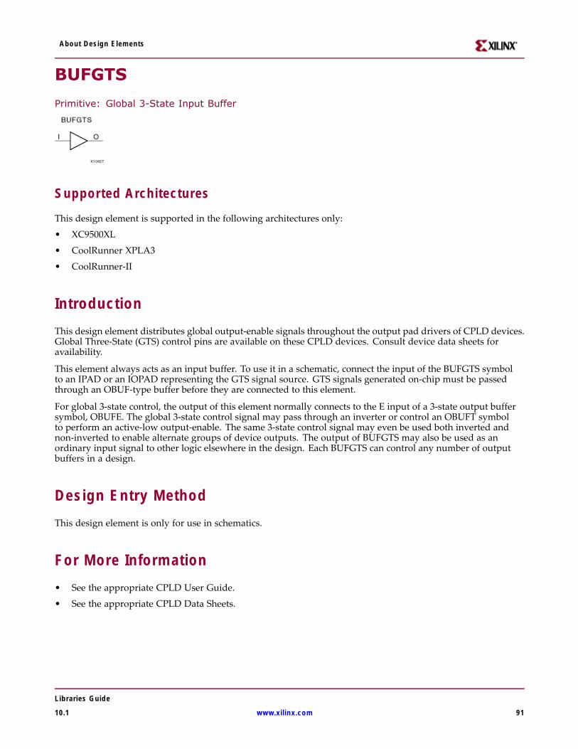
About Design Elements
BUFGTS
Primitive: Global 3-State Input Buffer
Supported Architectures
This design element is supported in the following architectures only:
• XC9500XL
• CoolRunner XPLA3
• CoolRunner-II
IntroductionThis design element distributes global output-enable signals throughout the output pad drivers of CPLD devices.Global Three-State (GTS) control pins are available on these CPLD devices. Consult device data sheets foravailability.
This element always acts as an input buffer. To use it in a schematic, connect the input of the BUFGTS symbolto an IPAD or an IOPAD representing the GTS signal source. GTS signals generated on-chip must be passedthrough an OBUF-type buffer before they are connected to this element.
For global 3-state control, the output of this element normally connects to the E input of a 3-state output buffersymbol, OBUFE. The global 3-state control signal may pass through an inverter or control an OBUFT symbolto perform an active-low output-enable. The same 3-state control signal may even be used both inverted andnon-inverted to enable alternate groups of device outputs. The output of BUFGTS may also be used as anordinary input signal to other logic elsewhere in the design. Each BUFGTS can control any number of outputbuffers in a design.
Design Entry MethodThis design element is only for use in schematics.
For More Information• See the appropriate CPLD User Guide.
• See the appropriate CPLD Data Sheets.
Libraries Guide
10.1 www.xilinx.com 91

About Design Elements
BUFT
Primitive: Internal 3-State Buffer with Active Low Enable
Supported ArchitecturesThis design element is supported in the following architectures only:• XC9500XL• CoolRunner XPLA3
IntroductionThis design element is a single 3-state buffer with input I and an output of O and active-Low output enable (T).When T is Low, data on the input of the buffer is transferred to the corresponding output. When T is High,the output is high impedance (Z state or off). The output of the buffer is connected to a horizontal longlinein FPGA architectures.
The output of separate BUFT symbols can be tied together to form a bus or a multiplexer. Make sure that onlyone T is Low at one time. For CPLD devices, BUFT output nets assume the High logic level when all connectedBUFE/BUFT buffers are disabled. For FPGAs, when all BUFTs on a net are disabled, the net is High. For correctsimulation of this effect, a PULLUP element must be connected to the net. NGDBuild inserts a PULLUP elementif one is not connected so that back-annotation simulation reflects the true state of the device.
Logic TableInputs Outputs
T I O
1 X Z
0 1 1
0 0 0
Design Entry MethodThis design element is only for use in schematics.
For More Information• See the appropriate CPLD User Guide.• See the appropriate CPLD Data Sheets.
Libraries Guide
92 www.xilinx.com 10.1

About Design Elements
BUFT16
Macro: 16-Bit Internal 3-State Buffers with Active Low Enable
Supported Architectures
This design element is supported in the following architectures only:
• XC9500XL
• CoolRunner XPLA3
IntroductionThis design element is a multiple 3-state buffer with inputs I15 – 10 and outputs O15 – O0 and active-Low outputenable (T). When T is Low, data on the inputs of the buffers is transferred to the corresponding outputs. When Tis High, the output is high impedance (Z state or off). The outputs of the buffers are connected to horizontallonglines in FPGA architectures.
This design element is a dedicated random access memory blocks with synchronous write capability. The blockRAM port has 16384 bits of data memory. The cell configuration for this element is listed in the following table.
Logic TableInputs Outputs
GSR EN SSR WE CLK ADDR DI DIP DO DOP RAM Contents
Data RAM Parity RAM
1 X X X X X X X INIT INIT No Change No Change
0 0 X X X X X X NoChange
NoChange No Change No Change
0 1 1 0 ↑ X X X SRVAL SRVAL No Change No Change
0 1 1 1 ↑ addr data pdata SRVAL SRVAL RAM(addr)=>data
RAM(addr)=>pdata
0 1 0 0 ↑ addr X X RAM(addr) RAM(addr) No Change No Change
Libraries Guide
10.1 www.xilinx.com 93

About Design Elements
Inputs Outputs
GSR EN SSR WE CLK ADDR DI DIP DO DOP RAM Contents
Data RAM Parity RAM
0 1 0 1 ↑ addr data pdata NoChange(a)RAM(addr)(b)data(c)
NoChange(a)RAM(addr)(b)pdata(c)
RAM(addr)=>data
RAM(addr)=>pdata
GSR=Global Set Reset signal
INIT=Value specified by the INIT attribute for data memory. Default is all zeros.
SRVAL=Value after assertion of SSR as specified by the SRVAL attribute.
addr=RAM address.
RAM(addr)=RAM contents at address ADDR.
data=RAM input data.
pdata=RAM parity data.
(a) WRITE_MODE=NO_CHANGE
(b) WRITE_MODE=READ_FIRST
(c) WRITE_MODE=WRITE_FIRST
Design Entry MethodInstantiation Yes
Inference Recommended
Coregen and wizards Yes
Macro support No
This design element can be used in schematics.
For More Information• See the appropriate CPLD User Guide.
• See the appropriate CPLD Data Sheets.
Libraries Guide
94 www.xilinx.com 10.1

About Design Elements
BUFT4
Macro: 4-Bit Internal 3-State Buffers with Active Low Enable
Supported Architectures
This design element is supported in the following architectures only:
• XC9500XL
• CoolRunner XPLA3
IntroductionThis design element is a multiple 3-state buffer with inputs I3 – I0 and outputs O3 – O0 and active-Low outputenable (T). When T is Low, data on the inputs of the buffers is transferred to the corresponding outputs. When Tis High, the output is high impedance (Z state or off). The outputs of the buffers are connected to horizontallonglines in FPGA architectures.
This design element is a dedicated random access memory blocks with synchronous write capability. The blockRAM port has 16384 bits of data memory. The cell configuration for this element is listed in the following table.
Logic TableInputs Outputs
GSR EN SSR WE CLK ADDR DI DIP DO DOP RAM Contents
Data RAM Parity RAM
1 X X X X X X X INIT INIT No Change No Change
0 0 X X X X X X NoChange
NoChange No Change No Change
0 1 1 0 ↑ X X X SRVAL SRVAL No Change No Change
0 1 1 1 ↑ addr data pdata SRVAL SRVAL RAM(addr)=>data
RAM(addr)=>pdata
0 1 0 0 ↑ addr X X RAM(addr) RAM(addr) No Change No Change
Libraries Guide
10.1 www.xilinx.com 95
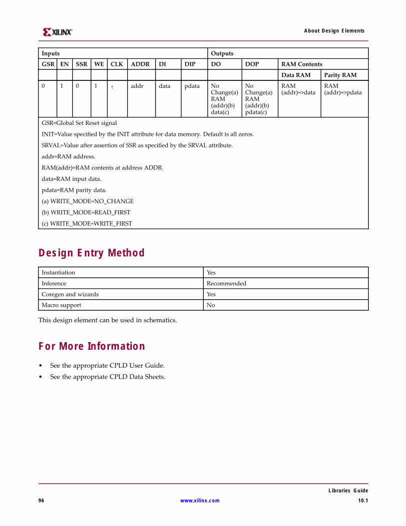
About Design Elements
Inputs Outputs
GSR EN SSR WE CLK ADDR DI DIP DO DOP RAM Contents
Data RAM Parity RAM
0 1 0 1 ↑ addr data pdata NoChange(a)RAM(addr)(b)data(c)
NoChange(a)RAM(addr)(b)pdata(c)
RAM(addr)=>data
RAM(addr)=>pdata
GSR=Global Set Reset signal
INIT=Value specified by the INIT attribute for data memory. Default is all zeros.
SRVAL=Value after assertion of SSR as specified by the SRVAL attribute.
addr=RAM address.
RAM(addr)=RAM contents at address ADDR.
data=RAM input data.
pdata=RAM parity data.
(a) WRITE_MODE=NO_CHANGE
(b) WRITE_MODE=READ_FIRST
(c) WRITE_MODE=WRITE_FIRST
Design Entry MethodInstantiation Yes
Inference Recommended
Coregen and wizards Yes
Macro support No
This design element can be used in schematics.
For More Information• See the appropriate CPLD User Guide.
• See the appropriate CPLD Data Sheets.
Libraries Guide
96 www.xilinx.com 10.1

About Design Elements
BUFT8
Macro: 8-Bit Internal 3-State Buffers with Active Low Enable
Supported Architectures
This design element is supported in the following architectures only:
• XC9500XL
• CoolRunner XPLA3
IntroductionThis design element is a multiple 3-state buffer with inputs I7 – I0 and outputs O7 – O0 and active-Low outputenable (T). When T is Low, data on the inputs of the buffers is transferred to the corresponding outputs. When Tis High, the output is high impedance (Z state or off). The outputs of the buffers are connected to horizontallonglines in FPGA architectures.
This design element is a dedicated random access memory blocks with synchronous write capability. The blockRAM port has 16384 bits of data memory. The cell configuration for this element is listed in the following table.
Logic TableInputs Outputs
GSR EN SSR WE CLK ADDR DI DIP DO DOP RAM Contents
Data RAM Parity RAM
1 X X X X X X X INIT INIT No Change No Change
0 0 X X X X X X NoChange
NoChange No Change No Change
0 1 1 0 ↑ X X X SRVAL SRVAL No Change No Change
0 1 1 1 ↑ addr data pdata SRVAL SRVAL RAM(addr)=>data
RAM(addr)=>pdata
0 1 0 0 ↑ addr X X RAM(addr) RAM(addr) No Change No Change
Libraries Guide
10.1 www.xilinx.com 97

About Design Elements
Inputs Outputs
GSR EN SSR WE CLK ADDR DI DIP DO DOP RAM Contents
Data RAM Parity RAM
0 1 0 1 ↑ addr data pdata NoChange(a)RAM(addr)(b)data(c)
NoChange(a)RAM(addr)(b)pdata(c)
RAM(addr)=>data
RAM(addr)=>pdata
GSR=Global Set Reset signal
INIT=Value specified by the INIT attribute for data memory. Default is all zeros.
SRVAL=Value after assertion of SSR as specified by the SRVAL attribute.
addr=RAM address.
RAM(addr)=RAM contents at address ADDR.
data=RAM input data.
pdata=RAM parity data.
(a) WRITE_MODE=NO_CHANGE
(b) WRITE_MODE=READ_FIRST
(c) WRITE_MODE=WRITE_FIRST
Design Entry MethodInstantiation Yes
Inference Recommended
Coregen and wizards Yes
Macro support No
This design element can be used in schematics.
For More Information• See the appropriate CPLD User Guide.
• See the appropriate CPLD Data Sheets.
Libraries Guide
98 www.xilinx.com 10.1

About Design Elements
CB16CE
Macro: 16-Bit Cascadable Binary Counter with Clock Enable and Asynchronous Clear
Supported Architectures
This design element is supported in the following architectures only:
• XC9500XL
• CoolRunner XPLA3
• CoolRunner-II
IntroductionThis design element is an asynchronously clearable, cascadable binary counter. The asynchronous clear (CLR)input, when High, overrides all other inputs and forces the Q outputs, terminal count (TC), and clock enable out(CEO) to logic level zero, independent of clock transitions. The Q outputs increment when the clock enable input(CE) is High during the Low-to-High clock (C) transition. The counter ignores clock transitions when CE is Low.The TC output is High when all Q outputs are High.
Create larger counters by connecting the CEO output of each stage to the CE input of the next stage andconnecting the C and CLR inputs in parallel. CEO is active (High) when TC and CE are High. The maximumlength of the counter is determined by the accumulated CE-to-TC propagation delays versus the clock period.The clock period must be greater than n (tCE-TC), where n is the number of stages and the time tCE-TC is theCE-to-TC propagation delay of each stage. When cascading counters, use the CEO output if the counter uses theCE input or use the TC output if it does not.
This counter is asynchronously cleared, outputs Low, when power is applied. For CPLD devices, you cansimulate power-on by applying a High-level pulse on the PRLD global net.
Logic TableInputs Outputs
CLR CE C Qz-Q0 TC CEO
1 X X 0 0 0
0 0 X No change No change 0
0 1 ↑ Inc TC CEO
z = bit width - 1
TC = Qz•Q(z-1)•Q(z-2)•...•Q0
CEO = TC•CE
Libraries Guide
10.1 www.xilinx.com 99

About Design Elements
Design Entry MethodThis design element is only for use in schematics.
For More Information• See the appropriate CPLD User Guide.
• See the appropriate CPLD Data Sheets.
Libraries Guide
100 www.xilinx.com 10.1
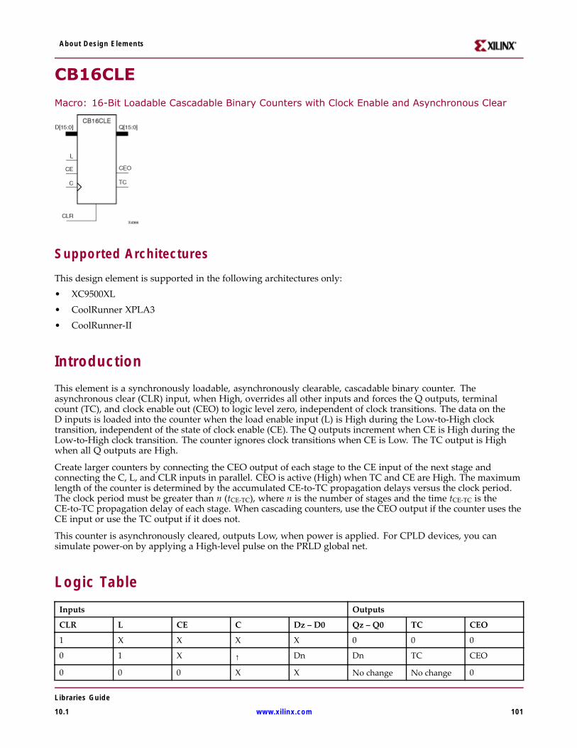
About Design Elements
CB16CLE
Macro: 16-Bit Loadable Cascadable Binary Counters with Clock Enable and Asynchronous Clear
Supported Architectures
This design element is supported in the following architectures only:• XC9500XL• CoolRunner XPLA3• CoolRunner-II
IntroductionThis element is a synchronously loadable, asynchronously clearable, cascadable binary counter. Theasynchronous clear (CLR) input, when High, overrides all other inputs and forces the Q outputs, terminalcount (TC), and clock enable out (CEO) to logic level zero, independent of clock transitions. The data on theD inputs is loaded into the counter when the load enable input (L) is High during the Low-to-High clocktransition, independent of the state of clock enable (CE). The Q outputs increment when CE is High during theLow-to-High clock transition. The counter ignores clock transitions when CE is Low. The TC output is Highwhen all Q outputs are High.
Create larger counters by connecting the CEO output of each stage to the CE input of the next stage andconnecting the C, L, and CLR inputs in parallel. CEO is active (High) when TC and CE are High. The maximumlength of the counter is determined by the accumulated CE-to-TC propagation delays versus the clock period.The clock period must be greater than n (tCE-TC), where n is the number of stages and the time tCE-TC is theCE-to-TC propagation delay of each stage. When cascading counters, use the CEO output if the counter uses theCE input or use the TC output if it does not.
This counter is asynchronously cleared, outputs Low, when power is applied. For CPLD devices, you cansimulate power-on by applying a High-level pulse on the PRLD global net.
Logic TableInputs Outputs
CLR L CE C Dz – D0 Qz – Q0 TC CEO
1 X X X X 0 0 0
0 1 X ↑ Dn Dn TC CEO
0 0 0 X X No change No change 0
Libraries Guide
10.1 www.xilinx.com 101

About Design Elements
Inputs Outputs
CLR L CE C Dz – D0 Qz – Q0 TC CEO
0 0 1 ↑ X Inc TC CEO
z = bit width - 1
TC = Qz•Q(z-1)•Q(z-2)•...•Q0
CEO = TC•CE
Design Entry MethodThis design element is only for use in schematics.
For More Information• See the appropriate CPLD User Guide.
• See the appropriate CPLD Data Sheets.
Libraries Guide
102 www.xilinx.com 10.1

About Design Elements
CB16CLED
Macro: 16-Bit Loadable Cascadable Bidirectional Binary Counters with Clock Enable andAsynchronous Clear
Supported Architectures
This design element is supported in the following architectures only:
• XC9500XL
• CoolRunner XPLA3
• CoolRunner-II
IntroductionThis design element is a synchronously loadable, asynchronously clearable, cascadable, bidirectional binarycounter. The asynchronous clear (CLR) input, when High, overrides all other inputs and forces the Q outputs,terminal count (TC), and clock enable out (CEO) to logic level zero, independent of clock transitions. The data onthe D inputs is loaded into the counter when the load enable input (L) is High during the Low-to-High clock(C) transition, independent of the state of clock enable (CE). The Q outputs decrement when CE is High andUP is Low during the Low-to- High clock transition. The Q outputs increment when CE and UP are High. Thecounter ignores clock transitions when CE is Low.
For counting up, the TC output is High when all Q outputs and UP are High. For counting down, the TCoutput is High when all Q outputs and UP are Low.
Create larger counters by connecting the CEO output of each stage to the CE input of the next stage andconnecting the C, UP, L, and CLR inputs in parallel. CEO is active (High) when TC and CE are High. Themaximum length of the counter is determined by the accumulated CE-to-TC propagation delays versus the clockperiod. The clock period must be greater than n (tCE-TC), where n is the number of stages and the time tCE-TC isthe CE-to-TC propagation delay of each stage. When cascading counters, use the CEO output if the counteruses the CE input or use the TC output if it does not.
For CPLD parts, see “CB2X1”, “CB4X1”, “CB8X1”, “CB16X1” for high-performance cascadable, bidirectionalcounters.
This counter is asynchronously cleared, outputs Low, when power is applied. For CPLD devices, you cansimulate power-on by applying a High-level pulse on the PRLD global net.
Libraries Guide
10.1 www.xilinx.com 103

About Design Elements
Logic TableInputs Outputs
CLR L CE C UP Dz – D0 Qz – Q0 TC CEO
1 X X X X X 0 0 0
0 1 X ↑ X Dn Dn TC CEO
0 0 0 X X X No change No change 0
0 0 1 ↑ 1 X Inc TC CEO
0 0 1 ↑ 0 X Dec TC CEO
z = bit width - 1
TC = (Qz•Q(z-1)•Q(z-2)•...•Q0•UP) + (Qz•Q(z-1)•Q(z-2)•...•Q0•UP)
CEO = TC•CE
Design Entry MethodThis design element is only for use in schematics.
For More Information• See the appropriate CPLD User Guide.
• See the appropriate CPLD Data Sheets.
Libraries Guide
104 www.xilinx.com 10.1

About Design Elements
CB16RE
Macro: 16-Bit Cascadable Binary Counter with Clock Enable and Synchronous Reset
Supported Architectures
This design element is supported in the following architectures only:• XC9500XL• CoolRunner XPLA3• CoolRunner-II
IntroductionThis design element is a synchronous, resettable, cascadable binary counter. The synchronous reset (R), whenHigh, overrides all other inputs and forces the Q outputs, terminal count (TC), and clock enable out (CEO) tozero on the Low-to-High clock transition. The Q outputs increment when the clock enable input (CE) is Highduring the Low-to-High clock (C) transition. The counter ignores clock transitions when CE is Low. The TCoutput is High when both Q outputs are High.
Create larger counters by connecting the CEO output of each stage to the CE input of the next stage andconnecting the C and R inputs in parallel. CEO is active (High) when TC and CE are High. The maximum lengthof the counter is determined by the accumulated CE-to-TC propagation delays versus the clock period. Theclock period must be greater than n (tCE-TC), where n is the number of stages and the time tCE-TC is the CE-to-TCpropagation delay of each stage. When cascading counters, use the CEO output if the counter uses the CEinput or use the TC output if it does not.
This counter is asynchronously cleared, outputs Low, when power is applied. For CPLD devices, you cansimulate power-on by applying a High-level pulse on the PRLD global net.
Logic TableInputs Outputs
R CE C Qz-Q0 TC CEO
1 X ↑ 0 0 0
0 0 X No change No change 0
0 1 ↑ Inc TC CEO
z = bit width - 1
TC = Qz•Q(z-1)•Q(z-2)•...•Q0)
CEO = TC•CE
Libraries Guide
10.1 www.xilinx.com 105

About Design Elements
Design Entry MethodThis design element is only for use in schematics.
For More Information• See the appropriate CPLD User Guide.
• See the appropriate CPLD Data Sheets.
Libraries Guide
106 www.xilinx.com 10.1
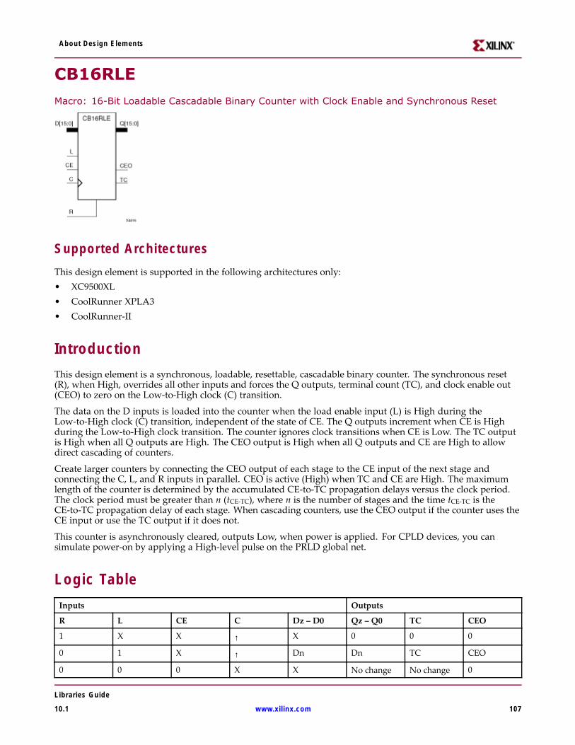
About Design Elements
CB16RLE
Macro: 16-Bit Loadable Cascadable Binary Counter with Clock Enable and Synchronous Reset
Supported ArchitecturesThis design element is supported in the following architectures only:• XC9500XL• CoolRunner XPLA3• CoolRunner-II
IntroductionThis design element is a synchronous, loadable, resettable, cascadable binary counter. The synchronous reset(R), when High, overrides all other inputs and forces the Q outputs, terminal count (TC), and clock enable out(CEO) to zero on the Low-to-High clock (C) transition.
The data on the D inputs is loaded into the counter when the load enable input (L) is High during theLow-to-High clock (C) transition, independent of the state of CE. The Q outputs increment when CE is Highduring the Low-to-High clock transition. The counter ignores clock transitions when CE is Low. The TC outputis High when all Q outputs are High. The CEO output is High when all Q outputs and CE are High to allowdirect cascading of counters.
Create larger counters by connecting the CEO output of each stage to the CE input of the next stage andconnecting the C, L, and R inputs in parallel. CEO is active (High) when TC and CE are High. The maximumlength of the counter is determined by the accumulated CE-to-TC propagation delays versus the clock period.The clock period must be greater than n (tCE-TC), where n is the number of stages and the time tCE-TC is theCE-to-TC propagation delay of each stage. When cascading counters, use the CEO output if the counter uses theCE input or use the TC output if it does not.
This counter is asynchronously cleared, outputs Low, when power is applied. For CPLD devices, you cansimulate power-on by applying a High-level pulse on the PRLD global net.
Logic TableInputs Outputs
R L CE C Dz – D0 Qz – Q0 TC CEO
1 X X ↑ X 0 0 0
0 1 X ↑ Dn Dn TC CEO
0 0 0 X X No change No change 0
Libraries Guide
10.1 www.xilinx.com 107

About Design Elements
Inputs Outputs
R L CE C Dz – D0 Qz – Q0 TC CEO
0 0 1 ↑ X Inc TC CEO
z = bit width - 1
TC = Qz•Q(z-1)•Q(z-2)•...•Q0
CEO = TC•CE
Design Entry MethodThis design element is only for use in schematics.
For More Information• See the appropriate CPLD User Guide.
• See the appropriate CPLD Data Sheets.
Libraries Guide
108 www.xilinx.com 10.1

About Design Elements
CB16X1
Macro: 16-Bit Loadable Cascadable Bidirectional Binary Counter with Clock Enable andAsynchronous Clear
Supported ArchitecturesThis design element is supported in the following architectures only:• XC9500XL• CoolRunner XPLA3• CoolRunner-II
IntroductionThis design element is a synchronously loadable, asynchronously clearable, bidirectional binary counter. It hasseparate count-enable inputs and synchronous terminal-count outputs for up and down directions to supporthigh-speed cascading.
The asynchronous clear (CLR) is the highest priority input. When CLR is High, all other inputs are ignored; dataoutputs (Q) go to logic level zero, terminal count outputs TCU and TCD go to zero and one, respectively, clockenable outputs CEOU and CEOD go to Low and High, respectively, independent of clock transitions. The dataon the D inputs loads into the counter on the Low-to-High clock (C) transition when the load enable input (L)is High, independent of the CE inputs.
The Q outputs increment when CEU is High, provided CLR and L are Low, during the Low-to-High clocktransition. The Q outputs decrement when CED is High, provided CLR and L are Low. The counter ignoresclock transitions when CEU and CED are Low. Both CEU and CED should not be High during the same clocktransition; the CEOU and CEOD outputs might not function properly for cascading when CEU and CED areboth High.
For counting up, the CEOU output is High when all Q outputs and CEU are High. For counting down, theCEOD output is High when all Q outputs are Low and CED is High. To cascade counters, connect the CEOU andCEOD outputs of each counter directly to the CEU and CED inputs, respectively, of the next stage. Connectthe clock, L, and CLR inputs in parallel.
The maximum clocking frequency of these counter components is unaffected by the number of cascaded stagesfor all counting and loading functions. The TCU terminal count output is High when all Q outputs are High,regardless of CEU. The TCD output is High when all Q outputs are Low, regardless of CED.
When cascading counters, the final terminal count signals can be produced by AND wiring all the TCU outputs(for the up direction) and all the TCD outputs (for the down direction). The TCU, CEOU, and CEOD outputs areproduced by optimizable AND gates within the component. This results in zero propagation from the CEUand CED inputs and from the Q outputs, provided all connections from each such output remain on-chip.Otherwise, a macrocell buffer delay is introduced.
Libraries Guide
10.1 www.xilinx.com 109

About Design Elements
The counter is initialized to zero (TCU Low and TCD High) when power is applied. You can simulate power-onby applying a High-level pulse on the PRLD global net.
Logic TableInputs Outputs
CLR L CEU CED C Dz-D0 Qz-Q0 TCU TCD CEOU CEOD
1 X X X X X 0 0 1 0 CEOD
0 1 X X ↑ Dn Dn TCU TCD CEOU CEOD
0 0 0 0 X X NoChange
NoChange
NoChange
0 0
0 0 1 0 ↑ X Inc TCU TCD CEOU 0
0 0 0 1 ↑ X Dec TCU TCD 0 CEOD
0 0 1 1 ↑ X Inc TCU TCD Invalid Invalid
z = bit width - 1
TCU = Qz•Q(z-1)•Q(z-2)•...•Q0
TCD = Qz•Q(z-1)•Q(z-2)•...•Q0
CEOU = TCU•CEU
CEOD = TCD•CED
Design Entry MethodThis design element is only for use in schematics.
For More Information• See the appropriate CPLD User Guide.
• See the appropriate CPLD Data Sheets.
Libraries Guide
110 www.xilinx.com 10.1

About Design Elements
CB16X2
Macro: 16-Bit Loadable Cascadable Bidirectional Binary Counter with Clock Enable andSynchro-nous Reset
Supported Architectures
This design element is supported in the following architectures only:
• XC9500XL
• CoolRunner XPLA3
• CoolRunner-II
IntroductionThis design element is a synchronous, loadable, resettable, bidirectional binary counter. It has separatecount-enable inputs and synchronous terminal-count outputs for up and down directions to support high-speedcascading in CPLD architectures.
The synchronous reset (R) is the highest priority input. When R is High, all other inputs are ignored; the dataoutputs (Q) go to logic level zero, terminal count outputs TCU and TCD go to zero and one, respectively,and clock enable outputs CEOU and CEOD go to Low and High, respectively, on the Low-to-High clock (C)transition. The data on the D inputs loads into the counter on the Low-to-High clock (C) transition when the loadenable input (L) is High, independent of the CE inputs.
All Q outputs increment when CEU is High, provided R and L are Low during the Low-to-High clock transition.All Q outputs decrement when CED is High, provided R and L are Low. The counter ignores clock transitionswhen CEU and CED are Low. Both CEU and CED should not be High during the same clock transition; theCEOU and CEOD outputs might not function properly for cascading when CEU and CED are both High.
For counting up, the CEOU output is High when all Q outputs and CEU are High. For counting down, theCEOD output is High when all Q outputs are Low and CED is High. To cascade counters, the CEOU and CEODoutputs of each counter are, respectively, connected directly to the CEU and CED inputs of the next stage. The C,L, and R inputs are connected in parallel.
The maximum clocking frequency of these counter components is unaffected by the number of cascaded stagesfor all counting and loading functions. The TCU terminal count output is High when all Q outputs are High,regardless of CEU. The TCD output is High when all Q outputs are Low, regardless of CED.
When cascading counters, the final terminal count signals can be produced by AND wiring all the TCU outputs(for the up direction) and all the TCD outputs (for the down direction). The TCU, CEOU, and CEOD outputs areproduced by optimizable AND gates within the component. This results in zero propagation from the CEUand CED inputs and from the Q outputs, provided all connections from each such output remain on-chip.Otherwise, a macrocell buffer delay is introduced.
The counter is initialized to zero (TCU Low and TCD High) when power is applied. You can simulate power-onby applying a High-level pulse on the PRLD global net.
Libraries Guide
10.1 www.xilinx.com 111

About Design Elements
Logic TableInputs Outputs
R L CEU CED C Dz-D0 Qz-Q0 TCU TCD CEOU CEOD
1 X X X ↑ X 0 0 1 0 CEOD
0 1 X X ↑ Dn Dn TCU TCD CEOU CEOD
0 0 0 0 X X No Chg No Chg No Chg 0 0
0 0 1 0 ↑ X Inc TCU TCD CEOU 0
0 0 0 1 ↑ X Dec TCU TCD 0 CEOD
0 0 1 1 ↑ X Inc TCU TCD Invalid Invalid
z = bit width - 1
TCU = Qz•Q(z-1)•Q(z-2)•...•Q0
TCD = Qz•Q(z-1)•Q(z-2)•...•Q0
CEOU = TCU•CEU
CEOD = TCD•CED
Design Entry MethodThis design element is only for use in schematics.
For More Information• See the appropriate CPLD User Guide.
• See the appropriate CPLD Data Sheets.
Libraries Guide
112 www.xilinx.com 10.1
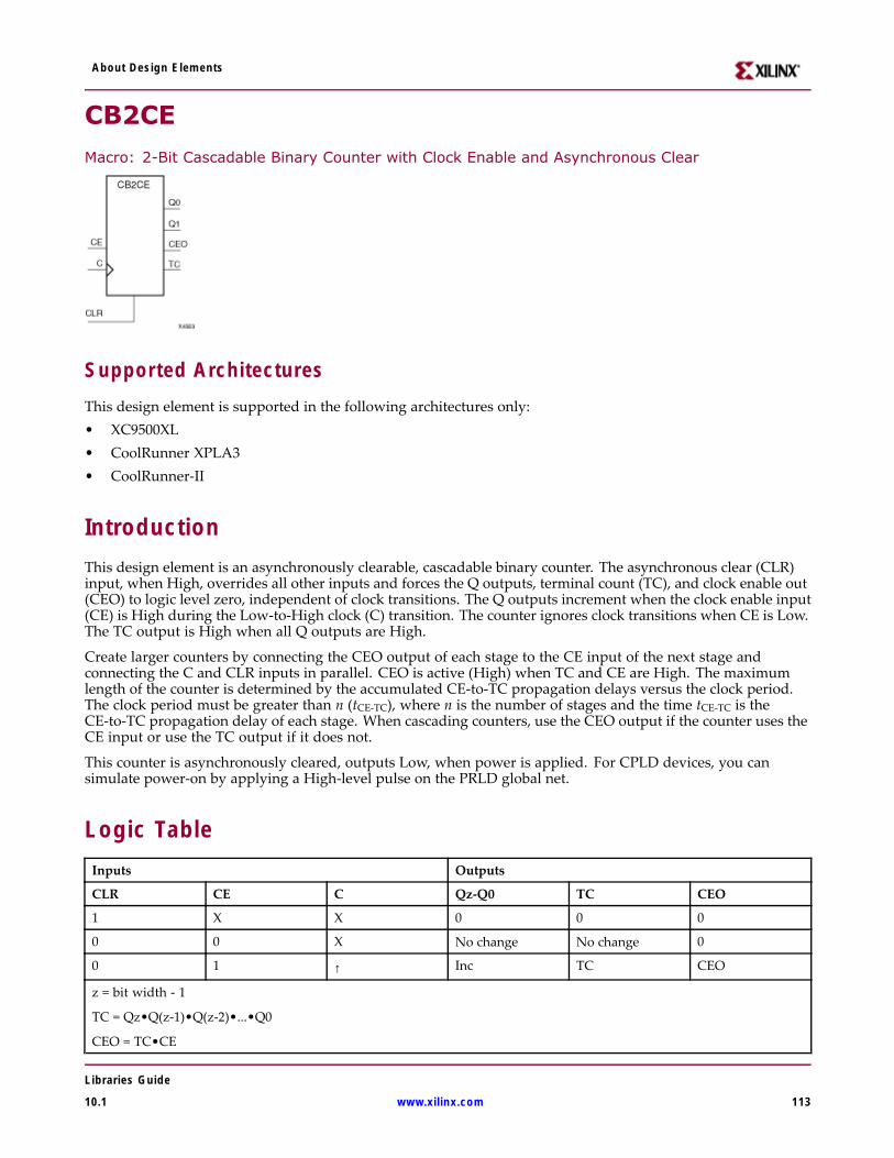
About Design Elements
CB2CE
Macro: 2-Bit Cascadable Binary Counter with Clock Enable and Asynchronous Clear
Supported ArchitecturesThis design element is supported in the following architectures only:• XC9500XL• CoolRunner XPLA3• CoolRunner-II
IntroductionThis design element is an asynchronously clearable, cascadable binary counter. The asynchronous clear (CLR)input, when High, overrides all other inputs and forces the Q outputs, terminal count (TC), and clock enable out(CEO) to logic level zero, independent of clock transitions. The Q outputs increment when the clock enable input(CE) is High during the Low-to-High clock (C) transition. The counter ignores clock transitions when CE is Low.The TC output is High when all Q outputs are High.
Create larger counters by connecting the CEO output of each stage to the CE input of the next stage andconnecting the C and CLR inputs in parallel. CEO is active (High) when TC and CE are High. The maximumlength of the counter is determined by the accumulated CE-to-TC propagation delays versus the clock period.The clock period must be greater than n (tCE-TC), where n is the number of stages and the time tCE-TC is theCE-to-TC propagation delay of each stage. When cascading counters, use the CEO output if the counter uses theCE input or use the TC output if it does not.
This counter is asynchronously cleared, outputs Low, when power is applied. For CPLD devices, you cansimulate power-on by applying a High-level pulse on the PRLD global net.
Logic TableInputs Outputs
CLR CE C Qz-Q0 TC CEO
1 X X 0 0 0
0 0 X No change No change 0
0 1 ↑ Inc TC CEO
z = bit width - 1
TC = Qz•Q(z-1)•Q(z-2)•...•Q0
CEO = TC•CE
Libraries Guide
10.1 www.xilinx.com 113
About Design Elements
Design Entry MethodThis design element is only for use in schematics.
For More Information• See the appropriate CPLD User Guide.
• See the appropriate CPLD Data Sheets.
Libraries Guide
114 www.xilinx.com 10.1

About Design Elements
CB2CLE
Macro: 2-Bit Loadable Cascadable Binary Counters with Clock Enable and Asynchronous Clear
Supported ArchitecturesThis design element is supported in the following architectures only:• XC9500XL• CoolRunner XPLA3• CoolRunner-II
IntroductionThis element is a synchronously loadable, asynchronously clearable, cascadable binary counter. Theasynchronous clear (CLR) input, when High, overrides all other inputs and forces the Q outputs, terminalcount (TC), and clock enable out (CEO) to logic level zero, independent of clock transitions. The data on theD inputs is loaded into the counter when the load enable input (L) is High during the Low-to-High clocktransition, independent of the state of clock enable (CE). The Q outputs increment when CE is High during theLow-to-High clock transition. The counter ignores clock transitions when CE is Low. The TC output is Highwhen all Q outputs are High.
Create larger counters by connecting the CEO output of each stage to the CE input of the next stage andconnecting the C, L, and CLR inputs in parallel. CEO is active (High) when TC and CE are High. The maximumlength of the counter is determined by the accumulated CE-to-TC propagation delays versus the clock period.The clock period must be greater than n (tCE-TC), where n is the number of stages and the time tCE-TC is theCE-to-TC propagation delay of each stage. When cascading counters, use the CEO output if the counter uses theCE input or use the TC output if it does not.
This counter is asynchronously cleared, outputs Low, when power is applied. For CPLD devices, you cansimulate power-on by applying a High-level pulse on the PRLD global net.
Logic TableInputs Outputs
CLR L CE C Dz – D0 Qz – Q0 TC CEO
1 X X X X 0 0 0
0 1 X ↑ Dn Dn TC CEO
0 0 0 X X No change No change 0
Libraries Guide
10.1 www.xilinx.com 115

About Design Elements
Inputs Outputs
CLR L CE C Dz – D0 Qz – Q0 TC CEO
0 0 1 ↑ X Inc TC CEO
z = bit width - 1
TC = Qz•Q(z-1)•Q(z-2)•...•Q0
CEO = TC•CE
Design Entry MethodThis design element is only for use in schematics.
For More Information• See the appropriate CPLD User Guide.
• See the appropriate CPLD Data Sheets.
Libraries Guide
116 www.xilinx.com 10.1

About Design Elements
CB2CLED
Macro: 2-Bit Loadable Cascadable Bidirectional Binary Counters with Clock Enable andAsynchronous Clear
Supported Architectures
This design element is supported in the following architectures only:
• XC9500XL
• CoolRunner XPLA3
• CoolRunner-II
IntroductionThis design element is a synchronously loadable, asynchronously clearable, cascadable, bidirectional binarycounter. The asynchronous clear (CLR) input, when High, overrides all other inputs and forces the Q outputs,terminal count (TC), and clock enable out (CEO) to logic level zero, independent of clock transitions. The data onthe D inputs is loaded into the counter when the load enable input (L) is High during the Low-to-High clock(C) transition, independent of the state of clock enable (CE). The Q outputs decrement when CE is High andUP is Low during the Low-to- High clock transition. The Q outputs increment when CE and UP are High. Thecounter ignores clock transitions when CE is Low.
For counting up, the TC output is High when all Q outputs and UP are High. For counting down, the TCoutput is High when all Q outputs and UP are Low.
Create larger counters by connecting the CEO output of each stage to the CE input of the next stage andconnecting the C, UP, L, and CLR inputs in parallel. CEO is active (High) when TC and CE are High. Themaximum length of the counter is determined by the accumulated CE-to-TC propagation delays versus the clockperiod. The clock period must be greater than n (tCE-TC), where n is the number of stages and the time tCE-TC isthe CE-to-TC propagation delay of each stage. When cascading counters, use the CEO output if the counteruses the CE input or use the TC output if it does not.
For CPLD parts, see “CB2X1”, “CB4X1”, “CB8X1”, “CB16X1” for high-performance cascadable, bidirectionalcounters.
This counter is asynchronously cleared, outputs Low, when power is applied. For CPLD devices, you cansimulate power-on by applying a High-level pulse on the PRLD global net.
Libraries Guide
10.1 www.xilinx.com 117

About Design Elements
Logic TableInputs Outputs
CLR L CE C UP Dz – D0 Qz – Q0 TC CEO
1 X X X X X 0 0 0
0 1 X ↑ X Dn Dn TC CEO
0 0 0 X X X No change No change 0
0 0 1 ↑ 1 X Inc TC CEO
0 0 1 ↑ 0 X Dec TC CEO
z = bit width - 1
TC = (Qz•Q(z-1)•Q(z-2)•...•Q0•UP) + (Qz•Q(z-1)•Q(z-2)•...•Q0•UP)
CEO = TC•CE
Design Entry MethodThis design element is only for use in schematics.
For More Information• See the appropriate CPLD User Guide.
• See the appropriate CPLD Data Sheets.
Libraries Guide
118 www.xilinx.com 10.1

About Design Elements
CB2RE
Macro: 2-Bit Cascadable Binary Counter with Clock Enable and Synchronous Reset
Supported ArchitecturesThis design element is supported in the following architectures only:• XC9500XL• CoolRunner XPLA3• CoolRunner-II
IntroductionThis design element is a synchronous, resettable, cascadable binary counter. The synchronous reset (R), whenHigh, overrides all other inputs and forces the Q outputs, terminal count (TC), and clock enable out (CEO) tozero on the Low-to-High clock transition. The Q outputs increment when the clock enable input (CE) is Highduring the Low-to-High clock (C) transition. The counter ignores clock transitions when CE is Low. The TCoutput is High when both Q outputs are High.
Create larger counters by connecting the CEO output of each stage to the CE input of the next stage andconnecting the C and R inputs in parallel. CEO is active (High) when TC and CE are High. The maximum lengthof the counter is determined by the accumulated CE-to-TC propagation delays versus the clock period. Theclock period must be greater than n (tCE-TC), where n is the number of stages and the time tCE-TC is the CE-to-TCpropagation delay of each stage. When cascading counters, use the CEO output if the counter uses the CEinput or use the TC output if it does not.
This counter is asynchronously cleared, outputs Low, when power is applied. For CPLD devices, you cansimulate power-on by applying a High-level pulse on the PRLD global net.
Logic TableInputs Outputs
R CE C Qz-Q0 TC CEO
1 X ↑ 0 0 0
0 0 X No change No change 0
0 1 ↑ Inc TC CEO
z = bit width - 1
TC = Qz•Q(z-1)•Q(z-2)•...•Q0)
CEO = TC•CE
Libraries Guide
10.1 www.xilinx.com 119

About Design Elements
Design Entry MethodThis design element is only for use in schematics.
For More Information• See the appropriate CPLD User Guide.
• See the appropriate CPLD Data Sheets.
Libraries Guide
120 www.xilinx.com 10.1

About Design Elements
CB2RLEMacro: 2-Bit Loadable Cascadable Binary Counter with Clock Enable and Synchronous Reset
Supported ArchitecturesThis design element is supported in the following architectures only:• XC9500XL• CoolRunner XPLA3• CoolRunner-II
IntroductionThis design element is a synchronous, loadable, resettable, cascadable binary counter. The synchronous reset(R), when High, overrides all other inputs and forces the Q outputs, terminal count (TC), and clock enable out(CEO) to zero on the Low-to-High clock (C) transition.
The data on the D inputs is loaded into the counter when the load enable input (L) is High during theLow-to-High clock (C) transition, independent of the state of CE. The Q outputs increment when CE is Highduring the Low-to-High clock transition. The counter ignores clock transitions when CE is Low. The TC outputis High when all Q outputs are High. The CEO output is High when all Q outputs and CE are High to allowdirect cascading of counters.
Create larger counters by connecting the CEO output of each stage to the CE input of the next stage andconnecting the C, L, and R inputs in parallel. CEO is active (High) when TC and CE are High. The maximumlength of the counter is determined by the accumulated CE-to-TC propagation delays versus the clock period.The clock period must be greater than n (tCE-TC), where n is the number of stages and the time tCE-TC is theCE-to-TC propagation delay of each stage. When cascading counters, use the CEO output if the counter uses theCE input or use the TC output if it does not.
This counter is asynchronously cleared, outputs Low, when power is applied. For CPLD devices, you cansimulate power-on by applying a High-level pulse on the PRLD global net.
Logic TableInputs Outputs
R L CE C Dz – D0 Qz – Q0 TC CEO
1 X X ↑ X 0 0 0
0 1 X ↑ Dn Dn TC CEO
Libraries Guide
10.1 www.xilinx.com 121

About Design Elements
Inputs Outputs
R L CE C Dz – D0 Qz – Q0 TC CEO
0 0 0 X X No change No change 0
0 0 1 ↑ X Inc TC CEO
z = bit width - 1
TC = Qz•Q(z-1)•Q(z-2)•...•Q0
CEO = TC•CE
Design Entry MethodThis design element is only for use in schematics.
For More Information• See the appropriate CPLD User Guide.
• See the appropriate CPLD Data Sheets.
Libraries Guide
122 www.xilinx.com 10.1

About Design Elements
CB2X1
Macro: 2-Bit Loadable Cascadable Bidirectional Binary Counter with Clock Enable andAsynchronous Clear
Supported Architectures
This design element is supported in the following architectures only:
• XC9500XL
• CoolRunner XPLA3
• CoolRunner-II
IntroductionThis design element is a synchronously loadable, asynchronously clearable, bidirectional binary counter. It hasseparate count-enable inputs and synchronous terminal-count outputs for up and down directions to supporthigh-speed cascading.
The asynchronous clear (CLR) is the highest priority input. When CLR is High, all other inputs are ignored; dataoutputs (Q) go to logic level zero, terminal count outputs TCU and TCD go to zero and one, respectively, clockenable outputs CEOU and CEOD go to Low and High, respectively, independent of clock transitions. The dataon the D inputs loads into the counter on the Low-to-High clock (C) transition when the load enable input (L)is High, independent of the CE inputs.
The Q outputs increment when CEU is High, provided CLR and L are Low, during the Low-to-High clocktransition. The Q outputs decrement when CED is High, provided CLR and L are Low. The counter ignoresclock transitions when CEU and CED are Low. Both CEU and CED should not be High during the same clocktransition; the CEOU and CEOD outputs might not function properly for cascading when CEU and CED areboth High.
For counting up, the CEOU output is High when all Q outputs and CEU are High. For counting down, theCEOD output is High when all Q outputs are Low and CED is High. To cascade counters, connect the CEOU andCEOD outputs of each counter directly to the CEU and CED inputs, respectively, of the next stage. Connectthe clock, L, and CLR inputs in parallel.
The maximum clocking frequency of these counter components is unaffected by the number of cascaded stagesfor all counting and loading functions. The TCU terminal count output is High when all Q outputs are High,regardless of CEU. The TCD output is High when all Q outputs are Low, regardless of CED.
Libraries Guide
10.1 www.xilinx.com 123

About Design Elements
When cascading counters, the final terminal count signals can be produced by AND wiring all the TCU outputs(for the up direction) and all the TCD outputs (for the down direction). The TCU, CEOU, and CEOD outputs areproduced by optimizable AND gates within the component. This results in zero propagation from the CEUand CED inputs and from the Q outputs, provided all connections from each such output remain on-chip.Otherwise, a macrocell buffer delay is introduced.
The counter is initialized to zero (TCU Low and TCD High) when power is applied. You can simulate power-onby applying a High-level pulse on the PRLD global net.
Logic TableInputs Outputs
CLR L CEU CED C Dz-D0 Qz-Q0 TCU TCD CEOU CEOD
1 X X X X X 0 0 1 0 CEOD
0 1 X X ↑ Dn Dn TCU TCD CEOU CEOD
0 0 0 0 X X NoChange
NoChange
NoChange
0 0
0 0 1 0 ↑ X Inc TCU TCD CEOU 0
0 0 0 1 ↑ X Dec TCU TCD 0 CEOD
0 0 1 1 ↑ X Inc TCU TCD Invalid Invalid
z = bit width - 1
TCU = Qz•Q(z-1)•Q(z-2)•...•Q0
TCD = Qz•Q(z-1)•Q(z-2)•...•Q0
CEOU = TCU•CEU
CEOD = TCD•CED
Design Entry MethodThis design element is only for use in schematics.
For More Information• See the appropriate CPLD User Guide.
• See the appropriate CPLD Data Sheets.
Libraries Guide
124 www.xilinx.com 10.1

About Design Elements
CB2X2Macro: 2-Bit Loadable Cascadable Bidirectional Binary Counter with Clock Enable and SynchronousReset
Supported ArchitecturesThis design element is supported in the following architectures only:• XC9500XL• CoolRunner XPLA3• CoolRunner-II
IntroductionThis design element is a synchronous, loadable, resettable, bidirectional binary counter. It has separatecount-enable inputs and synchronous terminal-count outputs for up and down directions to support high-speedcascading in CPLD architectures.
The synchronous reset (R) is the highest priority input. When R is High, all other inputs are ignored; the dataoutputs (Q) go to logic level zero, terminal count outputs TCU and TCD go to zero and one, respectively,and clock enable outputs CEOU and CEOD go to Low and High, respectively, on the Low-to-High clock (C)transition. The data on the D inputs loads into the counter on the Low-to-High clock (C) transition when the loadenable input (L) is High, independent of the CE inputs.
All Q outputs increment when CEU is High, provided R and L are Low during the Low-to-High clock transition.All Q outputs decrement when CED is High, provided R and L are Low. The counter ignores clock transitionswhen CEU and CED are Low. Both CEU and CED should not be High during the same clock transition; theCEOU and CEOD outputs might not function properly for cascading when CEU and CED are both High.
For counting up, the CEOU output is High when all Q outputs and CEU are High. For counting down, theCEOD output is High when all Q outputs are Low and CED is High. To cascade counters, the CEOU and CEODoutputs of each counter are, respectively, connected directly to the CEU and CED inputs of the next stage. The C,L, and R inputs are connected in parallel.
The maximum clocking frequency of these counter components is unaffected by the number of cascaded stagesfor all counting and loading functions. The TCU terminal count output is High when all Q outputs are High,regardless of CEU. The TCD output is High when all Q outputs are Low, regardless of CED.
When cascading counters, the final terminal count signals can be produced by AND wiring all the TCU outputs(for the up direction) and all the TCD outputs (for the down direction). The TCU, CEOU, and CEOD outputs areproduced by optimizable AND gates within the component. This results in zero propagation from the CEUand CED inputs and from the Q outputs, provided all connections from each such output remain on-chip.Otherwise, a macrocell buffer delay is introduced.
Libraries Guide
10.1 www.xilinx.com 125

About Design Elements
The counter is initialized to zero (TCU Low and TCD High) when power is applied. You can simulate power-onby applying a High-level pulse on the PRLD global net.
Logic TableInputs Outputs
R L CEU CED C Dz-D0 Qz-Q0 TCU TCD CEOU CEOD
1 X X X ↑ X 0 0 1 0 CEOD
0 1 X X ↑ Dn Dn TCU TCD CEOU CEOD
0 0 0 0 X X No Chg No Chg No Chg 0 0
0 0 1 0 ↑ X Inc TCU TCD CEOU 0
0 0 0 1 ↑ X Dec TCU TCD 0 CEOD
0 0 1 1 ↑ X Inc TCU TCD Invalid Invalid
z = bit width - 1
TCU = Qz•Q(z-1)•Q(z-2)•...•Q0
TCD = Qz•Q(z-1)•Q(z-2)•...•Q0
CEOU = TCU•CEU
CEOD = TCD•CED
Design Entry MethodThis design element is only for use in schematics.
For More Information• See the appropriate CPLD User Guide.
• See the appropriate CPLD Data Sheets.
Libraries Guide
126 www.xilinx.com 10.1

About Design Elements
CB4CEMacro: 4-Bit Cascadable Binary Counter with Clock Enable and Asynchronous Clear
Supported ArchitecturesThis design element is supported in the following architectures only:• XC9500XL• CoolRunner XPLA3• CoolRunner-II
IntroductionThis design element is an asynchronously clearable, cascadable binary counter. The asynchronous clear (CLR)input, when High, overrides all other inputs and forces the Q outputs, terminal count (TC), and clock enable out(CEO) to logic level zero, independent of clock transitions. The Q outputs increment when the clock enable input(CE) is High during the Low-to-High clock (C) transition. The counter ignores clock transitions when CE is Low.The TC output is High when all Q outputs are High.
Create larger counters by connecting the CEO output of each stage to the CE input of the next stage andconnecting the C and CLR inputs in parallel. CEO is active (High) when TC and CE are High. The maximumlength of the counter is determined by the accumulated CE-to-TC propagation delays versus the clock period.The clock period must be greater than n (tCE-TC), where n is the number of stages and the time tCE-TC is theCE-to-TC propagation delay of each stage. When cascading counters, use the CEO output if the counter uses theCE input or use the TC output if it does not.
This counter is asynchronously cleared, outputs Low, when power is applied. For CPLD devices, you cansimulate power-on by applying a High-level pulse on the PRLD global net.
Logic TableInputs Outputs
CLR CE C Qz-Q0 TC CEO
1 X X 0 0 0
0 0 X No change No change 0
0 1 ↑ Inc TC CEO
z = bit width - 1
TC = Qz•Q(z-1)•Q(z-2)•...•Q0
CEO = TC•CE
Libraries Guide
10.1 www.xilinx.com 127

About Design Elements
Design Entry MethodThis design element is only for use in schematics.
For More Information• See the appropriate CPLD User Guide.
• See the appropriate CPLD Data Sheets.
Libraries Guide
128 www.xilinx.com 10.1

About Design Elements
CB4CLEMacro: 4-Bit Loadable Cascadable Binary Counters with Clock Enable and Asynchronous Clear
Supported ArchitecturesThis design element is supported in the following architectures only:• XC9500XL• CoolRunner XPLA3• CoolRunner-II
IntroductionThis element is a synchronously loadable, asynchronously clearable, cascadable binary counter. Theasynchronous clear (CLR) input, when High, overrides all other inputs and forces the Q outputs, terminalcount (TC), and clock enable out (CEO) to logic level zero, independent of clock transitions. The data on theD inputs is loaded into the counter when the load enable input (L) is High during the Low-to-High clocktransition, independent of the state of clock enable (CE). The Q outputs increment when CE is High during theLow-to-High clock transition. The counter ignores clock transitions when CE is Low. The TC output is Highwhen all Q outputs are High.
Create larger counters by connecting the CEO output of each stage to the CE input of the next stage andconnecting the C, L, and CLR inputs in parallel. CEO is active (High) when TC and CE are High. The maximumlength of the counter is determined by the accumulated CE-to-TC propagation delays versus the clock period.The clock period must be greater than n (tCE-TC), where n is the number of stages and the time tCE-TC is theCE-to-TC propagation delay of each stage. When cascading counters, use the CEO output if the counter uses theCE input or use the TC output if it does not.
This counter is asynchronously cleared, outputs Low, when power is applied. For CPLD devices, you cansimulate power-on by applying a High-level pulse on the PRLD global net.
Logic TableInputs Outputs
CLR L CE C Dz – D0 Qz – Q0 TC CEO
1 X X X X 0 0 0
0 1 X ↑ Dn Dn TC CEO
Libraries Guide
10.1 www.xilinx.com 129
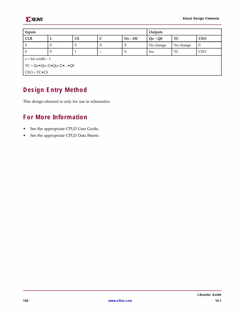
About Design Elements
Inputs Outputs
CLR L CE C Dz – D0 Qz – Q0 TC CEO
0 0 0 X X No change No change 0
0 0 1 ↑ X Inc TC CEO
z = bit width - 1
TC = Qz•Q(z-1)•Q(z-2)•...•Q0
CEO = TC•CE
Design Entry MethodThis design element is only for use in schematics.
For More Information• See the appropriate CPLD User Guide.
• See the appropriate CPLD Data Sheets.
Libraries Guide
130 www.xilinx.com 10.1

About Design Elements
CB4CLED
Macro: 4-Bit Loadable Cascadable Bidirectional Binary Counters with Clock Enable andAsynchronous Clear
Supported Architectures
This design element is supported in the following architectures only:
• XC9500XL
• CoolRunner XPLA3
• CoolRunner-II
IntroductionThis design element is a synchronously loadable, asynchronously clearable, cascadable, bidirectional binarycounter. The asynchronous clear (CLR) input, when High, overrides all other inputs and forces the Q outputs,terminal count (TC), and clock enable out (CEO) to logic level zero, independent of clock transitions. The data onthe D inputs is loaded into the counter when the load enable input (L) is High during the Low-to-High clock(C) transition, independent of the state of clock enable (CE). The Q outputs decrement when CE is High andUP is Low during the Low-to- High clock transition. The Q outputs increment when CE and UP are High. Thecounter ignores clock transitions when CE is Low.
For counting up, the TC output is High when all Q outputs and UP are High. For counting down, the TCoutput is High when all Q outputs and UP are Low.
Create larger counters by connecting the CEO output of each stage to the CE input of the next stage andconnecting the C, UP, L, and CLR inputs in parallel. CEO is active (High) when TC and CE are High. Themaximum length of the counter is determined by the accumulated CE-to-TC propagation delays versus the clockperiod. The clock period must be greater than n (tCE-TC), where n is the number of stages and the time tCE-TC isthe CE-to-TC propagation delay of each stage. When cascading counters, use the CEO output if the counteruses the CE input or use the TC output if it does not.
For CPLD parts, see “CB2X1”, “CB4X1”, “CB8X1”, “CB16X1” for high-performance cascadable, bidirectionalcounters.
This counter is asynchronously cleared, outputs Low, when power is applied. For CPLD devices, you cansimulate power-on by applying a High-level pulse on the PRLD global net.
Libraries Guide
10.1 www.xilinx.com 131

About Design Elements
Logic TableInputs Outputs
CLR L CE C UP Dz – D0 Qz – Q0 TC CEO
1 X X X X X 0 0 0
0 1 X ↑ X Dn Dn TC CEO
0 0 0 X X X No change No change 0
0 0 1 ↑ 1 X Inc TC CEO
0 0 1 ↑ 0 X Dec TC CEO
z = bit width - 1
TC = (Qz•Q(z-1)•Q(z-2)•...•Q0•UP) + (Qz•Q(z-1)•Q(z-2)•...•Q0•UP)
CEO = TC•CE
Design Entry MethodThis design element is only for use in schematics.
For More Information• See the appropriate CPLD User Guide.
• See the appropriate CPLD Data Sheets.
Libraries Guide
132 www.xilinx.com 10.1

About Design Elements
CB4REMacro: 4-Bit Cascadable Binary Counter with Clock Enable and Synchronous Reset
Supported ArchitecturesThis design element is supported in the following architectures only:• XC9500XL• CoolRunner XPLA3• CoolRunner-II
IntroductionThis design element is a synchronous, resettable, cascadable binary counter. The synchronous reset (R), whenHigh, overrides all other inputs and forces the Q outputs, terminal count (TC), and clock enable out (CEO) tozero on the Low-to-High clock transition. The Q outputs increment when the clock enable input (CE) is Highduring the Low-to-High clock (C) transition. The counter ignores clock transitions when CE is Low. The TCoutput is High when both Q outputs are High.
Create larger counters by connecting the CEO output of each stage to the CE input of the next stage andconnecting the C and R inputs in parallel. CEO is active (High) when TC and CE are High. The maximum lengthof the counter is determined by the accumulated CE-to-TC propagation delays versus the clock period. Theclock period must be greater than n (tCE-TC), where n is the number of stages and the time tCE-TC is the CE-to-TCpropagation delay of each stage. When cascading counters, use the CEO output if the counter uses the CEinput or use the TC output if it does not.
This counter is asynchronously cleared, outputs Low, when power is applied. For CPLD devices, you cansimulate power-on by applying a High-level pulse on the PRLD global net.
Logic TableInputs Outputs
R CE C Qz-Q0 TC CEO
1 X ↑ 0 0 0
0 0 X No change No change 0
0 1 ↑ Inc TC CEO
z = bit width - 1
TC = Qz•Q(z-1)•Q(z-2)•...•Q0)
CEO = TC•CE
Libraries Guide
10.1 www.xilinx.com 133

About Design Elements
Design Entry MethodThis design element is only for use in schematics.
For More Information• See the appropriate CPLD User Guide.
• See the appropriate CPLD Data Sheets.
Libraries Guide
134 www.xilinx.com 10.1

About Design Elements
CB4RLE
Macro: 4-Bit Loadable Cascadable Binary Counter with Clock Enable and Synchronous Reset
Supported ArchitecturesThis design element is supported in the following architectures only:• XC9500XL• CoolRunner XPLA3• CoolRunner-II
IntroductionThis design element is a synchronous, loadable, resettable, cascadable binary counter. The synchronous reset(R), when High, overrides all other inputs and forces the Q outputs, terminal count (TC), and clock enable out(CEO) to zero on the Low-to-High clock (C) transition.
The data on the D inputs is loaded into the counter when the load enable input (L) is High during theLow-to-High clock (C) transition, independent of the state of CE. The Q outputs increment when CE is Highduring the Low-to-High clock transition. The counter ignores clock transitions when CE is Low. The TC outputis High when all Q outputs are High. The CEO output is High when all Q outputs and CE are High to allowdirect cascading of counters.
Create larger counters by connecting the CEO output of each stage to the CE input of the next stage andconnecting the C, L, and R inputs in parallel. CEO is active (High) when TC and CE are High. The maximumlength of the counter is determined by the accumulated CE-to-TC propagation delays versus the clock period.The clock period must be greater than n (tCE-TC), where n is the number of stages and the time tCE-TC is theCE-to-TC propagation delay of each stage. When cascading counters, use the CEO output if the counter uses theCE input or use the TC output if it does not.
This counter is asynchronously cleared, outputs Low, when power is applied. For CPLD devices, you cansimulate power-on by applying a High-level pulse on the PRLD global net.
Logic TableInputs Outputs
R L CE C Dz – D0 Qz – Q0 TC CEO
1 X X ↑ X 0 0 0
Libraries Guide
10.1 www.xilinx.com 135
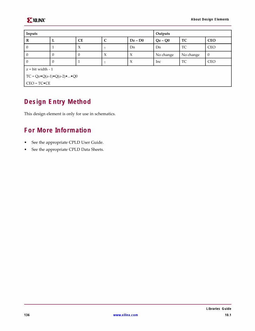
About Design Elements
Inputs Outputs
R L CE C Dz – D0 Qz – Q0 TC CEO
0 1 X ↑ Dn Dn TC CEO
0 0 0 X X No change No change 0
0 0 1 ↑ X Inc TC CEO
z = bit width - 1
TC = Qz•Q(z-1)•Q(z-2)•...•Q0
CEO = TC•CE
Design Entry MethodThis design element is only for use in schematics.
For More Information• See the appropriate CPLD User Guide.
• See the appropriate CPLD Data Sheets.
Libraries Guide
136 www.xilinx.com 10.1
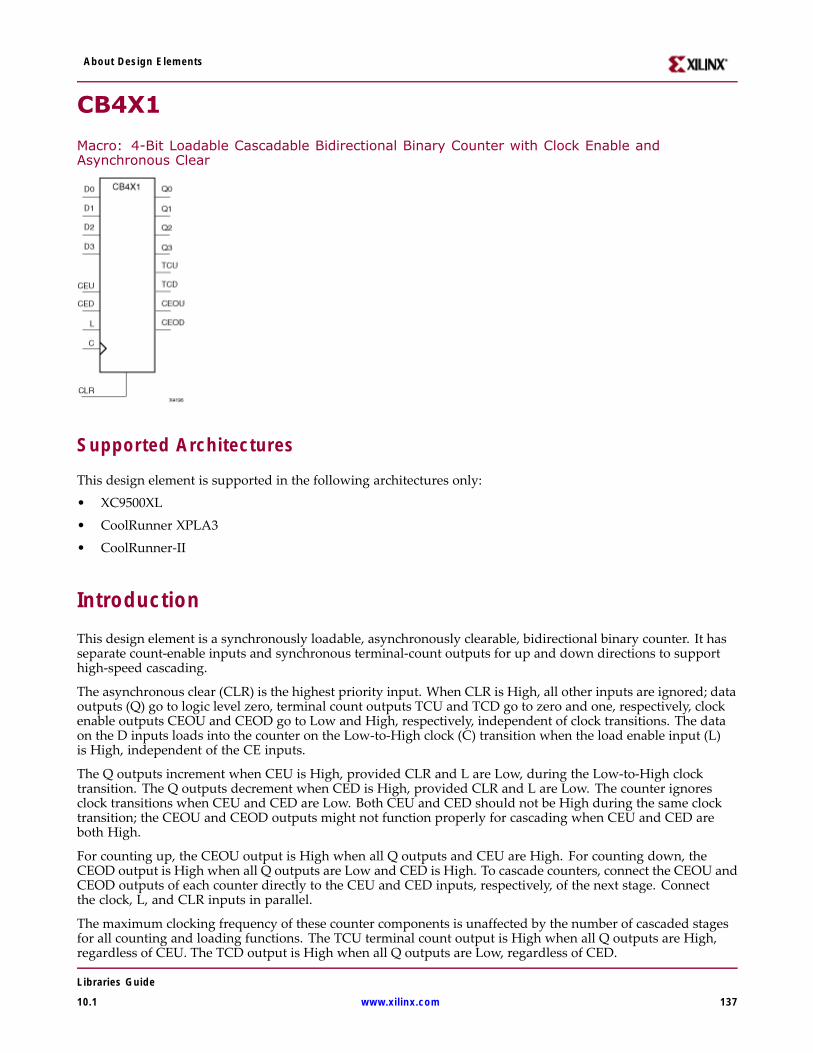
About Design Elements
CB4X1
Macro: 4-Bit Loadable Cascadable Bidirectional Binary Counter with Clock Enable andAsynchronous Clear
Supported Architectures
This design element is supported in the following architectures only:
• XC9500XL
• CoolRunner XPLA3
• CoolRunner-II
IntroductionThis design element is a synchronously loadable, asynchronously clearable, bidirectional binary counter. It hasseparate count-enable inputs and synchronous terminal-count outputs for up and down directions to supporthigh-speed cascading.
The asynchronous clear (CLR) is the highest priority input. When CLR is High, all other inputs are ignored; dataoutputs (Q) go to logic level zero, terminal count outputs TCU and TCD go to zero and one, respectively, clockenable outputs CEOU and CEOD go to Low and High, respectively, independent of clock transitions. The dataon the D inputs loads into the counter on the Low-to-High clock (C) transition when the load enable input (L)is High, independent of the CE inputs.
The Q outputs increment when CEU is High, provided CLR and L are Low, during the Low-to-High clocktransition. The Q outputs decrement when CED is High, provided CLR and L are Low. The counter ignoresclock transitions when CEU and CED are Low. Both CEU and CED should not be High during the same clocktransition; the CEOU and CEOD outputs might not function properly for cascading when CEU and CED areboth High.
For counting up, the CEOU output is High when all Q outputs and CEU are High. For counting down, theCEOD output is High when all Q outputs are Low and CED is High. To cascade counters, connect the CEOU andCEOD outputs of each counter directly to the CEU and CED inputs, respectively, of the next stage. Connectthe clock, L, and CLR inputs in parallel.
The maximum clocking frequency of these counter components is unaffected by the number of cascaded stagesfor all counting and loading functions. The TCU terminal count output is High when all Q outputs are High,regardless of CEU. The TCD output is High when all Q outputs are Low, regardless of CED.
Libraries Guide
10.1 www.xilinx.com 137

About Design Elements
When cascading counters, the final terminal count signals can be produced by AND wiring all the TCU outputs(for the up direction) and all the TCD outputs (for the down direction). The TCU, CEOU, and CEOD outputs areproduced by optimizable AND gates within the component. This results in zero propagation from the CEUand CED inputs and from the Q outputs, provided all connections from each such output remain on-chip.Otherwise, a macrocell buffer delay is introduced.
The counter is initialized to zero (TCU Low and TCD High) when power is applied. You can simulate power-onby applying a High-level pulse on the PRLD global net.
Logic TableInputs Outputs
CLR L CEU CED C Dz-D0 Qz-Q0 TCU TCD CEOU CEOD
1 X X X X X 0 0 1 0 CEOD
0 1 X X ↑ Dn Dn TCU TCD CEOU CEOD
0 0 0 0 X X NoChange
NoChange
NoChange
0 0
0 0 1 0 ↑ X Inc TCU TCD CEOU 0
0 0 0 1 ↑ X Dec TCU TCD 0 CEOD
0 0 1 1 ↑ X Inc TCU TCD Invalid Invalid
z = bit width - 1
TCU = Qz•Q(z-1)•Q(z-2)•...•Q0
TCD = Qz•Q(z-1)•Q(z-2)•...•Q0
CEOU = TCU•CEU
CEOD = TCD•CED
Design Entry MethodThis design element is only for use in schematics.
For More Information• See the appropriate CPLD User Guide.
• See the appropriate CPLD Data Sheets.
Libraries Guide
138 www.xilinx.com 10.1

About Design Elements
CB4X2
Macro: 4-Bit Loadable Cascadable Bidirectional Binary Counter with Clock Enable and SynchronousReset
Supported Architectures
This design element is supported in the following architectures only:
• XC9500XL
• CoolRunner XPLA3
• CoolRunner-II
IntroductionThis design element is a synchronous, loadable, resettable, bidirectional binary counter. It has separatecount-enable inputs and synchronous terminal-count outputs for up and down directions to support high-speedcascading in CPLD architectures.
The synchronous reset (R) is the highest priority input. When R is High, all other inputs are ignored; the dataoutputs (Q) go to logic level zero, terminal count outputs TCU and TCD go to zero and one, respectively,and clock enable outputs CEOU and CEOD go to Low and High, respectively, on the Low-to-High clock (C)transition. The data on the D inputs loads into the counter on the Low-to-High clock (C) transition when the loadenable input (L) is High, independent of the CE inputs.
All Q outputs increment when CEU is High, provided R and L are Low during the Low-to-High clock transition.All Q outputs decrement when CED is High, provided R and L are Low. The counter ignores clock transitionswhen CEU and CED are Low. Both CEU and CED should not be High during the same clock transition; theCEOU and CEOD outputs might not function properly for cascading when CEU and CED are both High.
For counting up, the CEOU output is High when all Q outputs and CEU are High. For counting down, theCEOD output is High when all Q outputs are Low and CED is High. To cascade counters, the CEOU and CEODoutputs of each counter are, respectively, connected directly to the CEU and CED inputs of the next stage. The C,L, and R inputs are connected in parallel.
The maximum clocking frequency of these counter components is unaffected by the number of cascaded stagesfor all counting and loading functions. The TCU terminal count output is High when all Q outputs are High,regardless of CEU. The TCD output is High when all Q outputs are Low, regardless of CED.
Libraries Guide
10.1 www.xilinx.com 139

About Design Elements
When cascading counters, the final terminal count signals can be produced by AND wiring all the TCU outputs(for the up direction) and all the TCD outputs (for the down direction). The TCU, CEOU, and CEOD outputs areproduced by optimizable AND gates within the component. This results in zero propagation from the CEUand CED inputs and from the Q outputs, provided all connections from each such output remain on-chip.Otherwise, a macrocell buffer delay is introduced.
The counter is initialized to zero (TCU Low and TCD High) when power is applied. You can simulate power-onby applying a High-level pulse on the PRLD global net.
Logic TableInputs Outputs
R L CEU CED C Dz-D0 Qz-Q0 TCU TCD CEOU CEOD
1 X X X ↑ X 0 0 1 0 CEOD
0 1 X X ↑ Dn Dn TCU TCD CEOU CEOD
0 0 0 0 X X No Chg No Chg No Chg 0 0
0 0 1 0 ↑ X Inc TCU TCD CEOU 0
0 0 0 1 ↑ X Dec TCU TCD 0 CEOD
0 0 1 1 ↑ X Inc TCU TCD Invalid Invalid
z = bit width - 1
TCU = Qz•Q(z-1)•Q(z-2)•...•Q0
TCD = Qz•Q(z-1)•Q(z-2)•...•Q0
CEOU = TCU•CEU
CEOD = TCD•CED
Design Entry MethodThis design element is only for use in schematics.
For More Information• See the appropriate CPLD User Guide.
• See the appropriate CPLD Data Sheets.
Libraries Guide
140 www.xilinx.com 10.1

About Design Elements
CB8CE
Macro: 8-Bit Cascadable Binary Counter with Clock Enable and Asynchronous Clear
Supported Architectures
This design element is supported in the following architectures only:
• XC9500XL
• CoolRunner XPLA3
• CoolRunner-II
IntroductionThis design element is an asynchronously clearable, cascadable binary counter. The asynchronous clear (CLR)input, when High, overrides all other inputs and forces the Q outputs, terminal count (TC), and clock enable out(CEO) to logic level zero, independent of clock transitions. The Q outputs increment when the clock enable input(CE) is High during the Low-to-High clock (C) transition. The counter ignores clock transitions when CE is Low.The TC output is High when all Q outputs are High.
Create larger counters by connecting the CEO output of each stage to the CE input of the next stage andconnecting the C and CLR inputs in parallel. CEO is active (High) when TC and CE are High. The maximumlength of the counter is determined by the accumulated CE-to-TC propagation delays versus the clock period.The clock period must be greater than n (tCE-TC), where n is the number of stages and the time tCE-TC is theCE-to-TC propagation delay of each stage. When cascading counters, use the CEO output if the counter uses theCE input or use the TC output if it does not.
This counter is asynchronously cleared, outputs Low, when power is applied. For CPLD devices, you cansimulate power-on by applying a High-level pulse on the PRLD global net.
Logic TableInputs Outputs
CLR CE C Qz-Q0 TC CEO
1 X X 0 0 0
0 0 X No change No change 0
0 1 ↑ Inc TC CEO
z = bit width - 1
TC = Qz•Q(z-1)•Q(z-2)•...•Q0
CEO = TC•CE
Libraries Guide
10.1 www.xilinx.com 141

About Design Elements
Design Entry MethodThis design element is only for use in schematics.
For More Information• See the appropriate CPLD User Guide.
• See the appropriate CPLD Data Sheets.
Libraries Guide
142 www.xilinx.com 10.1

About Design Elements
CB8CLE
Macro: 8-Bit Loadable Cascadable Binary Counters with Clock Enable and Asynchronous Clear
Supported Architectures
This design element is supported in the following architectures only:
• XC9500XL
• CoolRunner XPLA3
• CoolRunner-II
IntroductionThis element is a synchronously loadable, asynchronously clearable, cascadable binary counter. Theasynchronous clear (CLR) input, when High, overrides all other inputs and forces the Q outputs, terminalcount (TC), and clock enable out (CEO) to logic level zero, independent of clock transitions. The data on theD inputs is loaded into the counter when the load enable input (L) is High during the Low-to-High clocktransition, independent of the state of clock enable (CE). The Q outputs increment when CE is High during theLow-to-High clock transition. The counter ignores clock transitions when CE is Low. The TC output is Highwhen all Q outputs are High.
Create larger counters by connecting the CEO output of each stage to the CE input of the next stage andconnecting the C, L, and CLR inputs in parallel. CEO is active (High) when TC and CE are High. The maximumlength of the counter is determined by the accumulated CE-to-TC propagation delays versus the clock period.The clock period must be greater than n (tCE-TC), where n is the number of stages and the time tCE-TC is theCE-to-TC propagation delay of each stage. When cascading counters, use the CEO output if the counter uses theCE input or use the TC output if it does not.
This counter is asynchronously cleared, outputs Low, when power is applied. For CPLD devices, you cansimulate power-on by applying a High-level pulse on the PRLD global net.
Logic TableInputs Outputs
CLR L CE C Dz – D0 Qz – Q0 TC CEO
1 X X X X 0 0 0
0 1 X ↑ Dn Dn TC CEO
0 0 0 X X No change No change 0
Libraries Guide
10.1 www.xilinx.com 143

About Design Elements
Inputs Outputs
CLR L CE C Dz – D0 Qz – Q0 TC CEO
0 0 1 ↑ X Inc TC CEO
z = bit width - 1
TC = Qz•Q(z-1)•Q(z-2)•...•Q0
CEO = TC•CE
Design Entry MethodThis design element is only for use in schematics.
For More Information• See the appropriate CPLD User Guide.
• See the appropriate CPLD Data Sheets.
Libraries Guide
144 www.xilinx.com 10.1

About Design Elements
CB8CLEDMacro: 8-Bit Loadable Cascadable Bidirectional Binary Counters with Clock Enable andAsynchronous Clear
Supported ArchitecturesThis design element is supported in the following architectures only:• XC9500XL• CoolRunner XPLA3• CoolRunner-II
IntroductionThis design element is a synchronously loadable, asynchronously clearable, cascadable, bidirectional binarycounter. The asynchronous clear (CLR) input, when High, overrides all other inputs and forces the Q outputs,terminal count (TC), and clock enable out (CEO) to logic level zero, independent of clock transitions. The data onthe D inputs is loaded into the counter when the load enable input (L) is High during the Low-to-High clock(C) transition, independent of the state of clock enable (CE). The Q outputs decrement when CE is High andUP is Low during the Low-to- High clock transition. The Q outputs increment when CE and UP are High. Thecounter ignores clock transitions when CE is Low.
For counting up, the TC output is High when all Q outputs and UP are High. For counting down, the TCoutput is High when all Q outputs and UP are Low.
Create larger counters by connecting the CEO output of each stage to the CE input of the next stage andconnecting the C, UP, L, and CLR inputs in parallel. CEO is active (High) when TC and CE are High. Themaximum length of the counter is determined by the accumulated CE-to-TC propagation delays versus the clockperiod. The clock period must be greater than n (tCE-TC), where n is the number of stages and the time tCE-TC isthe CE-to-TC propagation delay of each stage. When cascading counters, use the CEO output if the counteruses the CE input or use the TC output if it does not.
For CPLD parts, see “CB2X1”, “CB4X1”, “CB8X1”, “CB16X1” for high-performance cascadable, bidirectionalcounters.
This counter is asynchronously cleared, outputs Low, when power is applied. For CPLD devices, you cansimulate power-on by applying a High-level pulse on the PRLD global net.
Logic TableInputs Outputs
CLR L CE C UP Dz – D0 Qz – Q0 TC CEO
1 X X X X X 0 0 0
Libraries Guide
10.1 www.xilinx.com 145

About Design Elements
Inputs Outputs
CLR L CE C UP Dz – D0 Qz – Q0 TC CEO
0 1 X ↑ X Dn Dn TC CEO
0 0 0 X X X No change No change 0
0 0 1 ↑ 1 X Inc TC CEO
0 0 1 ↑ 0 X Dec TC CEO
z = bit width - 1
TC = (Qz•Q(z-1)•Q(z-2)•...•Q0•UP) + (Qz•Q(z-1)•Q(z-2)•...•Q0•UP)
CEO = TC•CE
Design Entry MethodThis design element is only for use in schematics.
For More Information• See the appropriate CPLD User Guide.
• See the appropriate CPLD Data Sheets.
Libraries Guide
146 www.xilinx.com 10.1

About Design Elements
CB8RE
Macro: 8-Bit Cascadable Binary Counter with Clock Enable and Synchronous Reset
Supported Architectures
This design element is supported in the following architectures only:• XC9500XL• CoolRunner XPLA3• CoolRunner-II
IntroductionThis design element is a synchronous, resettable, cascadable binary counter. The synchronous reset (R), whenHigh, overrides all other inputs and forces the Q outputs, terminal count (TC), and clock enable out (CEO) tozero on the Low-to-High clock transition. The Q outputs increment when the clock enable input (CE) is Highduring the Low-to-High clock (C) transition. The counter ignores clock transitions when CE is Low. The TCoutput is High when both Q outputs are High.
Create larger counters by connecting the CEO output of each stage to the CE input of the next stage andconnecting the C and R inputs in parallel. CEO is active (High) when TC and CE are High. The maximum lengthof the counter is determined by the accumulated CE-to-TC propagation delays versus the clock period. Theclock period must be greater than n (tCE-TC), where n is the number of stages and the time tCE-TC is the CE-to-TCpropagation delay of each stage. When cascading counters, use the CEO output if the counter uses the CEinput or use the TC output if it does not.
This counter is asynchronously cleared, outputs Low, when power is applied. For CPLD devices, you cansimulate power-on by applying a High-level pulse on the PRLD global net.
Logic TableInputs Outputs
R CE C Qz-Q0 TC CEO
1 X ↑ 0 0 0
0 0 X No change No change 0
0 1 ↑ Inc TC CEO
z = bit width - 1
TC = Qz•Q(z-1)•Q(z-2)•...•Q0)
CEO = TC•CE
Libraries Guide
10.1 www.xilinx.com 147

About Design Elements
Design Entry MethodThis design element is only for use in schematics.
For More Information• See the appropriate CPLD User Guide.
• See the appropriate CPLD Data Sheets.
Libraries Guide
148 www.xilinx.com 10.1

About Design Elements
CB8RLE
Macro: 8-Bit Loadable Cascadable Binary Counter with Clock Enable and Synchronous Reset
Supported ArchitecturesThis design element is supported in the following architectures only:• XC9500XL• CoolRunner XPLA3• CoolRunner-II
IntroductionThis design element is a synchronous, loadable, resettable, cascadable binary counter. The synchronous reset(R), when High, overrides all other inputs and forces the Q outputs, terminal count (TC), and clock enable out(CEO) to zero on the Low-to-High clock (C) transition.
The data on the D inputs is loaded into the counter when the load enable input (L) is High during theLow-to-High clock (C) transition, independent of the state of CE. The Q outputs increment when CE is Highduring the Low-to-High clock transition. The counter ignores clock transitions when CE is Low. The TC outputis High when all Q outputs are High. The CEO output is High when all Q outputs and CE are High to allowdirect cascading of counters.
Create larger counters by connecting the CEO output of each stage to the CE input of the next stage andconnecting the C, L, and R inputs in parallel. CEO is active (High) when TC and CE are High. The maximumlength of the counter is determined by the accumulated CE-to-TC propagation delays versus the clock period.The clock period must be greater than n (tCE-TC), where n is the number of stages and the time tCE-TC is theCE-to-TC propagation delay of each stage. When cascading counters, use the CEO output if the counter uses theCE input or use the TC output if it does not.
This counter is asynchronously cleared, outputs Low, when power is applied. For CPLD devices, you cansimulate power-on by applying a High-level pulse on the PRLD global net.
Logic TableInputs Outputs
R L CE C Dz – D0 Qz – Q0 TC CEO
1 X X ↑ X 0 0 0
0 1 X ↑ Dn Dn TC CEO
0 0 0 X X No change No change 0
Libraries Guide
10.1 www.xilinx.com 149
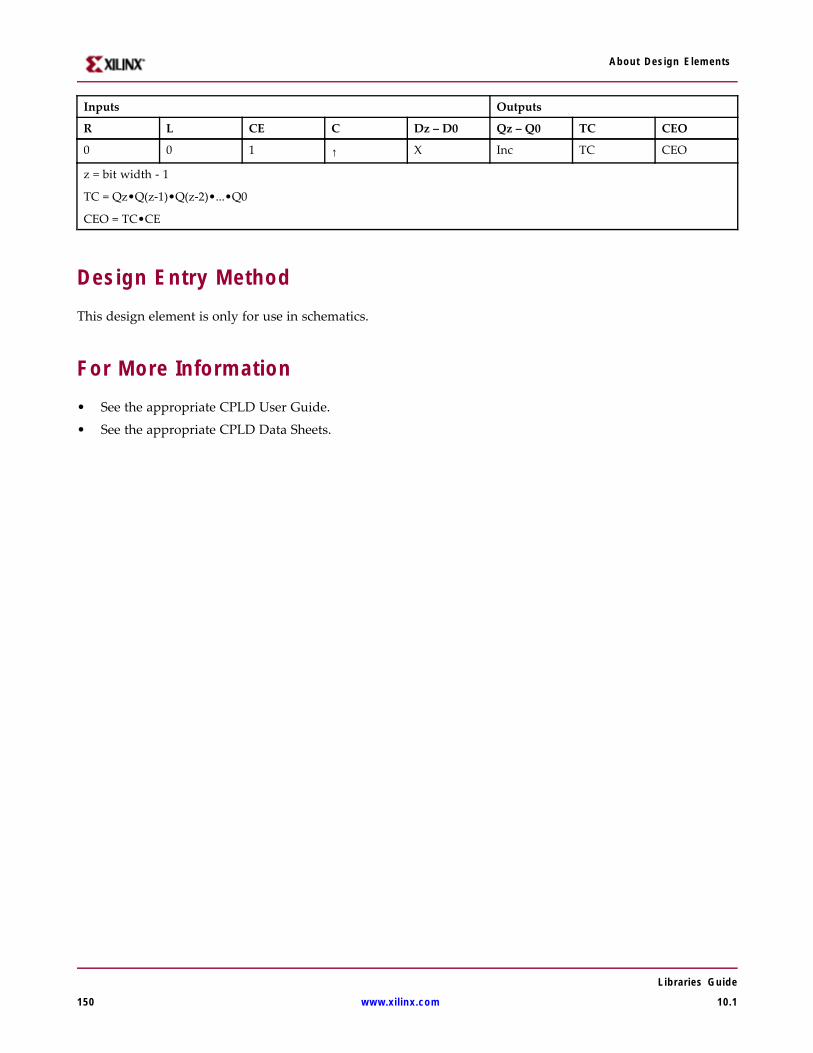
About Design Elements
Inputs Outputs
R L CE C Dz – D0 Qz – Q0 TC CEO
0 0 1 ↑ X Inc TC CEO
z = bit width - 1
TC = Qz•Q(z-1)•Q(z-2)•...•Q0
CEO = TC•CE
Design Entry MethodThis design element is only for use in schematics.
For More Information• See the appropriate CPLD User Guide.
• See the appropriate CPLD Data Sheets.
Libraries Guide
150 www.xilinx.com 10.1

About Design Elements
CB8X1
Macro: 8-Bit Loadable Cascadable Bidirectional Binary Counter with Clock Enable andAsynchronous Clear
Supported ArchitecturesThis design element is supported in the following architectures only:• XC9500XL• CoolRunner XPLA3• CoolRunner-II
IntroductionThis design element is a synchronously loadable, asynchronously clearable, bidirectional binary counter. It hasseparate count-enable inputs and synchronous terminal-count outputs for up and down directions to supporthigh-speed cascading.
The asynchronous clear (CLR) is the highest priority input. When CLR is High, all other inputs are ignored; dataoutputs (Q) go to logic level zero, terminal count outputs TCU and TCD go to zero and one, respectively, clockenable outputs CEOU and CEOD go to Low and High, respectively, independent of clock transitions. The dataon the D inputs loads into the counter on the Low-to-High clock (C) transition when the load enable input (L)is High, independent of the CE inputs.
The Q outputs increment when CEU is High, provided CLR and L are Low, during the Low-to-High clocktransition. The Q outputs decrement when CED is High, provided CLR and L are Low. The counter ignoresclock transitions when CEU and CED are Low. Both CEU and CED should not be High during the same clocktransition; the CEOU and CEOD outputs might not function properly for cascading when CEU and CED areboth High.
For counting up, the CEOU output is High when all Q outputs and CEU are High. For counting down, theCEOD output is High when all Q outputs are Low and CED is High. To cascade counters, connect the CEOU andCEOD outputs of each counter directly to the CEU and CED inputs, respectively, of the next stage. Connectthe clock, L, and CLR inputs in parallel.
The maximum clocking frequency of these counter components is unaffected by the number of cascaded stagesfor all counting and loading functions. The TCU terminal count output is High when all Q outputs are High,regardless of CEU. The TCD output is High when all Q outputs are Low, regardless of CED.
When cascading counters, the final terminal count signals can be produced by AND wiring all the TCU outputs(for the up direction) and all the TCD outputs (for the down direction). The TCU, CEOU, and CEOD outputs areproduced by optimizable AND gates within the component. This results in zero propagation from the CEUand CED inputs and from the Q outputs, provided all connections from each such output remain on-chip.Otherwise, a macrocell buffer delay is introduced.
Libraries Guide
10.1 www.xilinx.com 151

About Design Elements
The counter is initialized to zero (TCU Low and TCD High) when power is applied. You can simulate power-onby applying a High-level pulse on the PRLD global net.
Logic TableInputs Outputs
CLR L CEU CED C Dz-D0 Qz-Q0 TCU TCD CEOU CEOD
1 X X X X X 0 0 1 0 CEOD
0 1 X X ↑ Dn Dn TCU TCD CEOU CEOD
0 0 0 0 X X NoChange
NoChange
NoChange
0 0
0 0 1 0 ↑ X Inc TCU TCD CEOU 0
0 0 0 1 ↑ X Dec TCU TCD 0 CEOD
0 0 1 1 ↑ X Inc TCU TCD Invalid Invalid
z = bit width - 1
TCU = Qz•Q(z-1)•Q(z-2)•...•Q0
TCD = Qz•Q(z-1)•Q(z-2)•...•Q0
CEOU = TCU•CEU
CEOD = TCD•CED
Design Entry MethodThis design element is only for use in schematics.
For More Information• See the appropriate CPLD User Guide.
• See the appropriate CPLD Data Sheets.
Libraries Guide
152 www.xilinx.com 10.1
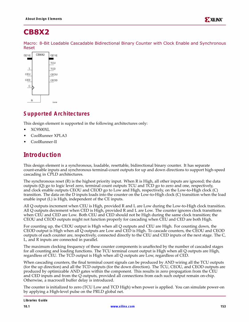
About Design Elements
CB8X2Macro: 8-Bit Loadable Cascadable Bidirectional Binary Counter with Clock Enable and SynchronousReset
Supported ArchitecturesThis design element is supported in the following architectures only:• XC9500XL• CoolRunner XPLA3• CoolRunner-II
IntroductionThis design element is a synchronous, loadable, resettable, bidirectional binary counter. It has separatecount-enable inputs and synchronous terminal-count outputs for up and down directions to support high-speedcascading in CPLD architectures.
The synchronous reset (R) is the highest priority input. When R is High, all other inputs are ignored; the dataoutputs (Q) go to logic level zero, terminal count outputs TCU and TCD go to zero and one, respectively,and clock enable outputs CEOU and CEOD go to Low and High, respectively, on the Low-to-High clock (C)transition. The data on the D inputs loads into the counter on the Low-to-High clock (C) transition when the loadenable input (L) is High, independent of the CE inputs.
All Q outputs increment when CEU is High, provided R and L are Low during the Low-to-High clock transition.All Q outputs decrement when CED is High, provided R and L are Low. The counter ignores clock transitionswhen CEU and CED are Low. Both CEU and CED should not be High during the same clock transition; theCEOU and CEOD outputs might not function properly for cascading when CEU and CED are both High.
For counting up, the CEOU output is High when all Q outputs and CEU are High. For counting down, theCEOD output is High when all Q outputs are Low and CED is High. To cascade counters, the CEOU and CEODoutputs of each counter are, respectively, connected directly to the CEU and CED inputs of the next stage. The C,L, and R inputs are connected in parallel.
The maximum clocking frequency of these counter components is unaffected by the number of cascaded stagesfor all counting and loading functions. The TCU terminal count output is High when all Q outputs are High,regardless of CEU. The TCD output is High when all Q outputs are Low, regardless of CED.
When cascading counters, the final terminal count signals can be produced by AND wiring all the TCU outputs(for the up direction) and all the TCD outputs (for the down direction). The TCU, CEOU, and CEOD outputs areproduced by optimizable AND gates within the component. This results in zero propagation from the CEUand CED inputs and from the Q outputs, provided all connections from each such output remain on-chip.Otherwise, a macrocell buffer delay is introduced.
The counter is initialized to zero (TCU Low and TCD High) when power is applied. You can simulate power-onby applying a High-level pulse on the PRLD global net.
Libraries Guide
10.1 www.xilinx.com 153

About Design Elements
Logic TableInputs Outputs
R L CEU CED C Dz-D0 Qz-Q0 TCU TCD CEOU CEOD
1 X X X ↑ X 0 0 1 0 CEOD
0 1 X X ↑ Dn Dn TCU TCD CEOU CEOD
0 0 0 0 X X No Chg No Chg No Chg 0 0
0 0 1 0 ↑ X Inc TCU TCD CEOU 0
0 0 0 1 ↑ X Dec TCU TCD 0 CEOD
0 0 1 1 ↑ X Inc TCU TCD Invalid Invalid
z = bit width - 1
TCU = Qz•Q(z-1)•Q(z-2)•...•Q0
TCD = Qz•Q(z-1)•Q(z-2)•...•Q0
CEOU = TCU•CEU
CEOD = TCD•CED
Design Entry MethodThis design element is only for use in schematics.
For More Information• See the appropriate CPLD User Guide.
• See the appropriate CPLD Data Sheets.
Libraries Guide
154 www.xilinx.com 10.1

About Design Elements
CBD16CE
Macro: 16-Bit Cascadable Dual Edge Triggered Binary Counter with Clock Enable and AsynchronousClear
Supported Architectures
This design element is supported in the following architectures only:
CoolRunner-II
IntroductionThis element is an asynchronously clearable, cascadable dual edge triggered binary counter. The asynchronousclear (CLR) input, when High, overrides all other inputs and forces the Q outputs, terminal count (TC), and clockenable out (CEO) to logic level zero, independent of clock transitions. The Q outputs increment when the clockenable input (CE) is High during the Low-to-High and High-to-Low clock (C) transition. The counter ignoresclock transitions when CE is Low. The TC output is High when all Q outputs are High.
Create larger counters by connecting the CEO output of each stage to the CE input of the next stage andconnecting the C and CLR inputs in parallel. CEO is active (High) when TC and CE are High. The maximumlength of the counter is determined by the accumulated CE-to-TC propagation delays versus the clock period.The clock period must be greater than n (tCE-TC), where n is the number of stages and the time tCE-TC is theCE-to-TC propagation delay of each stage. When cascading counters, use the CEO output if the counter uses theCE input or use the TC output if it does not.
This counter is asynchronously cleared, outputs Low, when power is applied. For CPLD devices, you cansimulate power-on by applying a High-level pulse on the PRLD global net.
Logic TableInputs Outputs
CLR CE C Qz – Q0 TC CEO
1 X X 0 0 0
0 0 X No change No change 0
0 1 ↑ Inc TC CEO
0 1 ↓ Inc TC CEO
z = bit width - 1
TC = Qz•Q(z-1)•Q(z-2)•...•Q0
CEO = TC•CE
Libraries Guide
10.1 www.xilinx.com 155

About Design Elements
Design Entry MethodThis design element is only for use in schematics.
For More Information• See the appropriate CPLD User Guide.
• See the appropriate CPLD Data Sheets.
Libraries Guide
156 www.xilinx.com 10.1
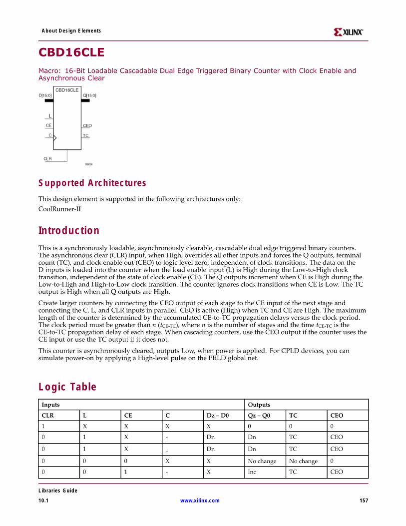
About Design Elements
CBD16CLEMacro: 16-Bit Loadable Cascadable Dual Edge Triggered Binary Counter with Clock Enable andAsynchronous Clear
Supported ArchitecturesThis design element is supported in the following architectures only:CoolRunner-II
IntroductionThis is a synchronously loadable, asynchronously clearable, cascadable dual edge triggered binary counters.The asynchronous clear (CLR) input, when High, overrides all other inputs and forces the Q outputs, terminalcount (TC), and clock enable out (CEO) to logic level zero, independent of clock transitions. The data on theD inputs is loaded into the counter when the load enable input (L) is High during the Low-to-High clocktransition, independent of the state of clock enable (CE). The Q outputs increment when CE is High during theLow-to-High and High-to-Low clock transition. The counter ignores clock transitions when CE is Low. The TCoutput is High when all Q outputs are High.
Create larger counters by connecting the CEO output of each stage to the CE input of the next stage andconnecting the C, L, and CLR inputs in parallel. CEO is active (High) when TC and CE are High. The maximumlength of the counter is determined by the accumulated CE-to-TC propagation delays versus the clock period.The clock period must be greater than n (tCE-TC), where n is the number of stages and the time tCE-TC is theCE-to-TC propagation delay of each stage. When cascading counters, use the CEO output if the counter uses theCE input or use the TC output if it does not.
This counter is asynchronously cleared, outputs Low, when power is applied. For CPLD devices, you cansimulate power-on by applying a High-level pulse on the PRLD global net.
Logic TableInputs Outputs
CLR L CE C Dz – D0 Qz – Q0 TC CEO
1 X X X X 0 0 0
0 1 X ↑ Dn Dn TC CEO
0 1 X ↓ Dn Dn TC CEO
0 0 0 X X No change No change 0
0 0 1 ↑ X Inc TC CEO
Libraries Guide
10.1 www.xilinx.com 157

About Design Elements
Inputs Outputs
CLR L CE C Dz – D0 Qz – Q0 TC CEO
0 0 1 ↓ X Inc TC CEO
z = bit width - 1
TC = Qz•Q(z-1)•Q(z-2)•...•Q0
CEO = TC•CE
Design Entry MethodThis design element is only for use in schematics.
For More Information• See the appropriate CPLD User Guide.
• See the appropriate CPLD Data Sheets.
Libraries Guide
158 www.xilinx.com 10.1
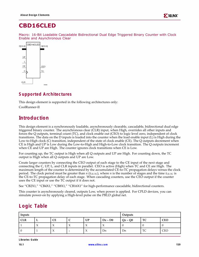
About Design Elements
CBD16CLEDMacro: 16-Bit Loadable Cascadable Bidirectional Dual Edge Triggered Binary Counter with ClockEnable and Asynchronous Clear
Supported ArchitecturesThis design element is supported in the following architectures only:CoolRunner-II
IntroductionThis design element is a synchronously loadable, asynchronously clearable, cascadable, bidirectional dual edgetriggered binary counter. The asynchronous clear (CLR) input, when High, overrides all other inputs andforces the Q outputs, terminal count (TC), and clock enable out (CEO) to logic level zero, independent of clocktransitions. The data on the D inputs is loaded into the counter when the load enable input (L) is High during theLow-to-High clock (C) transition, independent of the state of clock enable (CE). The Q outputs decrement whenCE is High and UP is Low during the Low-to-High and High-to-Low clock transition. The Q outputs incrementwhen CE and UP are High. The counter ignores clock transitions when CE is Low.
For counting up, the TC output is High when all Q outputs and UP are High. For counting down, the TCoutput is High when all Q outputs and UP are Low.
Create larger counters by connecting the CEO output of each stage to the CE input of the next stage andconnecting the C, UP, L, and CLR inputs in parallel. CEO is active (High) when TC and CE are High. Themaximum length of the counter is determined by the accumulated CE-to-TC propagation delays versus the clockperiod. The clock period must be greater than n (tCE-TC), where n is the number of stages and the time tCE-TC isthe CE-to-TC propagation delay of each stage. When cascading counters, use the CEO output if the counteruses the CE input or use the TC output if it does not.
See “CB2X1,” “CB4X1,” “CB8X1,” “CB16X1” for high-performance cascadable, bidirectional counters.
This counter is asynchronously cleared, outputs Low, when power is applied. For CPLD devices, you cansimulate power-on by applying a High-level pulse on the PRLD global net.
Logic TableInputs Outputs
CLR L CE C UP Dz – D0 Qz – Q0 TC CEO
1 X X X X X 0 0 0
0 1 X ↑ X Dn Dn TC CEO
Libraries Guide
10.1 www.xilinx.com 159
About Design Elements
Inputs Outputs
CLR L CE C UP Dz – D0 Qz – Q0 TC CEO
0 1 X ↓ X Dn Dn TC CEO
0 0 0 X X X No change No change 0
0 0 1 ↑ 1 X Inc TC CEO
0 0 1 ↓ 1 X Inc TC CEO
0 0 1 ↑ 0 X Dec TC CEO
0 0 1 ↓ 0 X Dec TC CEO
z = bit width - 1
TC = (Qz•Q(z-1)•Q(z-2)•...•Q0•UP) + (Qz•Q(z-1)•Q(z-2)•...•Q0•UP)
CEO = TC•CE
Design Entry MethodThis design element is only for use in schematics.
For More Information• See the appropriate CPLD User Guide.
• See the appropriate CPLD Data Sheets.
Libraries Guide
160 www.xilinx.com 10.1

About Design Elements
CBD16RE
Macro: 16-Bit Cascadable Dual Edge Triggered Binary Counter with Clock Enable and SynchronousReset
Supported ArchitecturesThis design element is supported in the following architectures only:CoolRunner-II
IntroductionThis design element is a synchronous, resettable, cascadable dual edge triggered binary counter. The synchronousreset (R), when High, overrides all other inputs and forces the Q outputs, terminal count (TC), and clock enableout (CEO) to logic level zero during the Low-to-High or High-to-Low clock transition. The Q outputs incrementwhen the clock enable input (CE) is High during the Low-to-High and High-to-Low clock (C) transition. Thecounter ignores clock transitions when CE is Low. The TC output is High when both Q outputs are High.
Create larger counters by connecting the CEO output of each stage to the CE input of the next stage andconnecting the C and R inputs in parallel. CEO is active (High) when TC and CE are High. The maximum lengthof the counter is determined by the accumulated CE-to-TC propagation delays versus the clock period. Theclock period must be greater than n (tCE-TC), where n is the number of stages and the time tCE-TC is the CE-to-TCpropagation delay of each stage. When cascading counters, use the CEO output if the counter uses the CEinput or use the TC output if it does not.
This counter is asynchronously cleared, outputs Low, when power is applied. For CPLD devices, you cansimulate power-on by applying a High-level pulse on the PRLD global net.
Logic TableInputs Outputs
R CE C Qz-Q0 TC CEO
1 X ↑ 0 0 0
1 X ↓ 0 0 0
0 0 X No change No change 0
0 1 ↑ Inc TC CEO
0 1 ↓ Inc TC CEO
z = bit width - 1
TC = Qz•Q(z-1)•Q(z-2)•...•Q0)
CEO = TC•CE
Libraries Guide
10.1 www.xilinx.com 161

About Design Elements
Design Entry MethodThis design element is only for use in schematics.
For More Information• See the appropriate CPLD User Guide.
• See the appropriate CPLD Data Sheets.
Libraries Guide
162 www.xilinx.com 10.1

About Design Elements
CBD16RLEMacro: 16-Bit Loadable Cascadable Dual Edge Triggered Binary Counter with Clock Enable andSynchronous Reset
Supported ArchitecturesThis design element is supported in the following architectures only:CoolRunner-II
IntroductionThis design element is a synchronous, loadable, resettable, cascadable dual edge triggered binary counter. Thesynchronous reset (R), when High, overrides all other inputs and forces the Q outputs, terminal count (TC), andclock enable out (CEO) outputs to Low on the Low-to-High or High-to-Low clock (C) transition.
The data on the D inputs is loaded into the counter when the load enable input (L) is High during theLow-to-High and High-to-Low clock (C) transition, independent of the state of CE. The Q outputs incrementwhen CE is High during the Low-to-High and High-to-Low clock transition. The counter ignores clocktransitions when CE is Low. The TC output is High when all Q outputs are High. The CEO output is High whenall Q outputs and CE are High to allow direct cascading of counters.
Create larger counters by connecting the CEO output of each stage to the CE input of the next stage andconnecting the C, L, and R inputs in parallel. CEO is active (High) when TC and CE are High. The maximumlength of the counter is determined by the accumulated CE-to-TC propagation delays versus the clock period.The clock period must be greater than n (tCE-TC), where n is the number of stages and the time tCE-TC is theCE-to-TC propagation delay of each stage. When cascading counters, use the CEO output if the counter uses theCE input or use the TC output if it does not.
This counter is asynchronously cleared, outputs Low, when power is applied. For CPLD devices, you cansimulate power-on by applying a High-level pulse on the PRLD global net.
Logic TableInputs Outputs
R L CE C Dz – D0 Qz – Q0 TC CEO
1 X X ↑ X 0 0 0
1 X X ↓ X 0 0 0
0 1 X ↑ Dn Dn TC CEO
0 1 X ↓ Dn Dn TC CEO
0 0 0 X X No change No change 0
Libraries Guide
10.1 www.xilinx.com 163
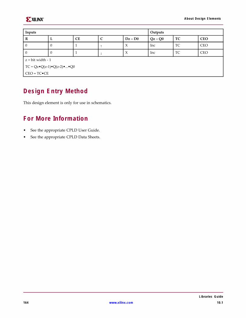
About Design Elements
Inputs Outputs
R L CE C Dz – D0 Qz – Q0 TC CEO
0 0 1 ↑ X Inc TC CEO
0 0 1 ↓ X Inc TC CEO
z = bit width - 1
TC = Qz•Q(z-1)•Q(z-2)•...•Q0
CEO = TC•CE
Design Entry MethodThis design element is only for use in schematics.
For More Information• See the appropriate CPLD User Guide.
• See the appropriate CPLD Data Sheets.
Libraries Guide
164 www.xilinx.com 10.1

About Design Elements
CBD16X1Macro: 16-Bit Loadable Cascadable Bidirectional Dual Edge Triggered Binary Counter with ClockEnable and Asynchronous Clear
Supported ArchitecturesThis design element is supported in the following architectures only:CoolRunner-II
IntroductionThis design element is a synchronously loadable, asynchronously clearable, bidirectional dual edge triggeredbinary counters. It has separate count-enable inputs and synchronous terminal-count outputs for up and downdirections to support high speed cascading.
The asynchronous clear (CLR) is the highest priority input. When CLR is High, all other inputs are ignored; dataoutputs (Q) go to logic level zero, terminal count outputs TCU and TCD go to zero and one, respectively, clockenable outputs CEOU and CEOD go to Low and High, respectively, independent of clock transitions. The dataon the D inputs loads into the counter on the Low-to-High and High-to-Low clock (C) transition when the loadenable input (L) is High, independent of the CE inputs.
The Q outputs increment when CEU is High, provided CLR and L are Low, during the Low-to-High andHigh-to-Low clock transition. The Q outputs decrement when CED is High, provided CLR and L are Low.The counter ignores clock transitions when CEU and CED are Low. Both CEU and CED should not be Highduring the same clock transition; the CEOU and CEOD outputs might not function properly for cascading whenCEU and CED are both High.
For counting up, the CEOU output is High when all Q outputs and CEU are High. For counting down, theCEOD output is High when all Q outputs are Low and CED is High. To cascade counters, the CEOU and CEODoutputs of each counter are connected directly to the CEU and CED inputs, respectively, of the next stage. Theclock, L, and CLR inputs are connected in parallel.
The maximum clocking frequency of these counters is unaffected by the number of cascaded stages for allcounting and loading functions. The TCU terminal count output is High when all Q outputs are High, regardlessof CEU. The TCD output is High when all Q outputs are Low, regardless of CED.
When cascading counters, the final terminal count signals can be produced by AND wiring all the TCU outputs(for the up direction) and all the TCD outputs (for the down direction). The TCU, CEOU, and CEOD outputs areproduced by optimizable AND gates within the component. This results in zero propagation from the CEUand CED inputs and from the Q outputs, provided all connections from each such output remain on-chip.Otherwise, a macrocell buffer delay is introduced.
This counter is asynchronously cleared, outputs Low, when power is applied. For CPLD devices, you cansimulate power-on by applying a High-level pulse on the PRLD global net.
Libraries Guide
10.1 www.xilinx.com 165

About Design Elements
Logic TableInputs Outputs
CLR L CEU CED C Dz–D0 Qz–Q0 TCU TCD CEOU CEOD
1 X X X X X 0 0 1 0 CEOD
0 1 X X ↑ Dn Dn TCU TCD CEOU CEOD
0 1 X X ↓ Dn Dn TCU TCD CEOU CEOD
0 0 0 0 X X NoChange
NoChange
NoChange
0 0
0 0 1 0 ↑ X Inc TCU TCD CEOU 0
0 0 1 0 ↓ X Inc TCU TCD CEOU 0
0 0 0 1 ↑ X Dec TCU TCD 0 CEOD
0 0 0 1 ↓ X Dec TCU TCD 0 CEOD
0 0 1 1 ↑ X Inc TCU TCD Invalid Invalid
0 0 1 1 ↓ X Inc TCU TCD Invalid Invalid
z = bit width - 1
TCU = Qz•Q(z-1)•Q(z-2)•...•Q0
TCD = Qz•Q(z-1)•Q(z-2)•...•Q0
CEOU = TCU•CEU
CEOD = TCD•CED
Design Entry MethodThis design element is only for use in schematics.
For More Information• See the appropriate CPLD User Guide.
• See the appropriate CPLD Data Sheets.
Libraries Guide
166 www.xilinx.com 10.1

About Design Elements
CBD16X2
Macro: 16-Bit Loadable Cascadable Bidirectional Dual Edge Triggered Binary Counter with ClockEnable and Synchronous Reset
Supported ArchitecturesThis design element is supported in the following architectures only:CoolRunner-II
IntroductionThis design element is a synchronous, loadable, resettable, bidirectional dual edge triggered binary counter. Ithas separate count-enable inputs and synchronous terminal-count outputs for up and down directions tosupport high-speed cascading.
The synchronous reset (R) is the highest priority input. When R is High, all other inputs are ignored; the dataoutputs (Q) go to logic level zero, terminal count outputs TCU and TCD go to zero and one, respectively, andclock enable outputs CEOU and CEOD go to Low and High, respectively, on the Low-to-High and High-to-Lowclock (C) transition. The data on the D inputs loads into the counter on the Low-to-High and High-to-Low clock(C) transition when the load enable input (L) is High, independent of the CE inputs.
All Q outputs increment when CEU is High, provided R and L are Low during the Low-to-High andHigh-to-Low clock transition. All Q outputs decrement when CED is High, provided R and L are Low. Thecounter ignores clock transitions when CEU and CED are Low. Both CEU and CED should not be High duringthe same clock transition; the CEOU and CEOD outputs might not function properly for cascading when CEUand CED are both High.
For counting up, the CEOU output is High when all Q outputs and CEU are High. For counting down, theCEOD output is High when all Q outputs are Low and CED is High. To cascade counters, the CEOU and CEODoutputs of each counter are, respectively, connected directly to the CEU and CED inputs of the next stage. The C,L, and R inputs are connected in parallel.
The maximum clocking frequency of these counter components is unaffected by the number of cascaded stagesfor all counting and loading functions. The TCU terminal count output is High when all Q outputs are High,regardless of CEU. The TCD output is High when all Q outputs are Low, regardless of CED.
When cascading counters, the final terminal count signals can be produced by AND wiring all the TCU outputs(for the up direction) and all the TCD outputs (for the down direction). The TCU, CEOU, and CEOD outputs areproduced by optimizable AND gates within the component. This results in zero propagation from the CEUand CED inputs and from the Q outputs, provided all connections from each such output remain on-chip.Otherwise, a macrocell buffer delay is introduced.
This counter is asynchronously cleared, outputs Low, when power is applied. For CPLD devices, you cansimulate power-on by applying a High-level pulse on the PRLD global net.
Libraries Guide
10.1 www.xilinx.com 167
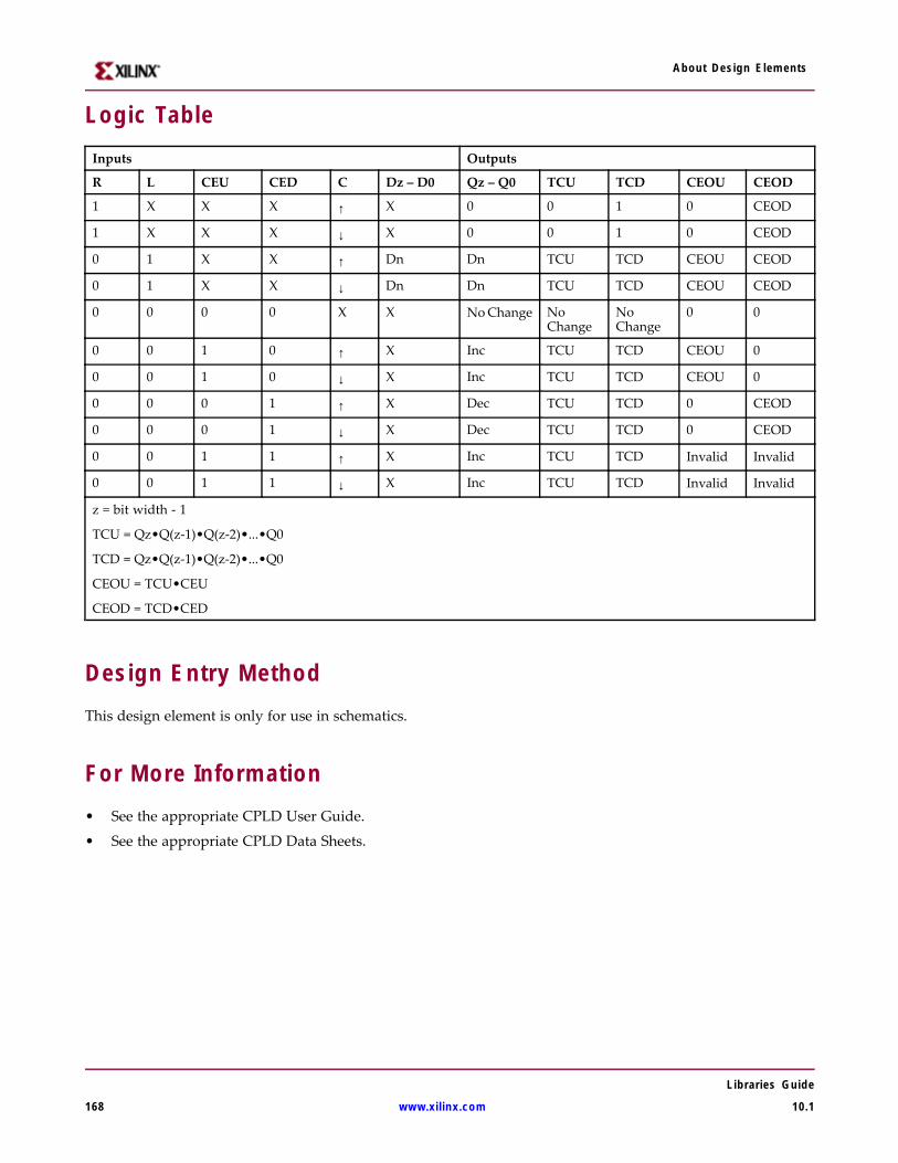
About Design Elements
Logic TableInputs Outputs
R L CEU CED C Dz – D0 Qz – Q0 TCU TCD CEOU CEOD
1 X X X ↑ X 0 0 1 0 CEOD
1 X X X ↓ X 0 0 1 0 CEOD
0 1 X X ↑ Dn Dn TCU TCD CEOU CEOD
0 1 X X ↓ Dn Dn TCU TCD CEOU CEOD
0 0 0 0 X X NoChange NoChange
NoChange
0 0
0 0 1 0 ↑ X Inc TCU TCD CEOU 0
0 0 1 0 ↓ X Inc TCU TCD CEOU 0
0 0 0 1 ↑ X Dec TCU TCD 0 CEOD
0 0 0 1 ↓ X Dec TCU TCD 0 CEOD
0 0 1 1 ↑ X Inc TCU TCD Invalid Invalid
0 0 1 1 ↓ X Inc TCU TCD Invalid Invalid
z = bit width - 1
TCU = Qz•Q(z-1)•Q(z-2)•...•Q0
TCD = Qz•Q(z-1)•Q(z-2)•...•Q0
CEOU = TCU•CEU
CEOD = TCD•CED
Design Entry MethodThis design element is only for use in schematics.
For More Information• See the appropriate CPLD User Guide.
• See the appropriate CPLD Data Sheets.
Libraries Guide
168 www.xilinx.com 10.1
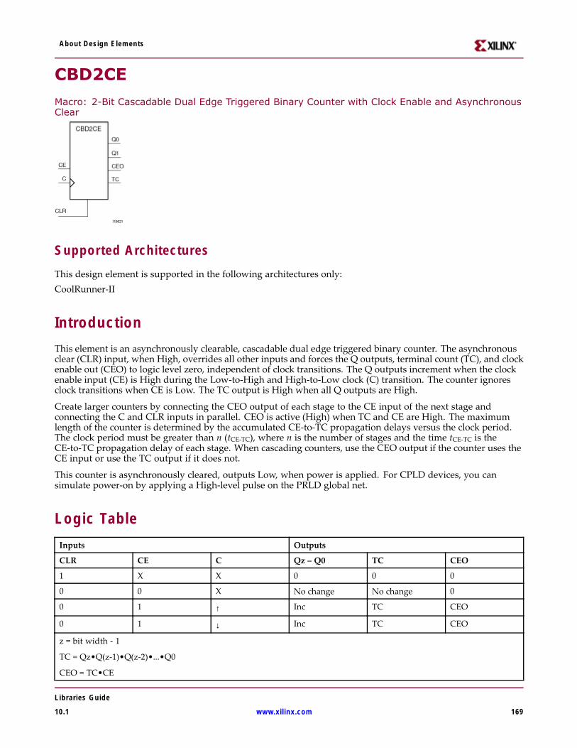
About Design Elements
CBD2CE
Macro: 2-Bit Cascadable Dual Edge Triggered Binary Counter with Clock Enable and AsynchronousClear
Supported ArchitecturesThis design element is supported in the following architectures only:CoolRunner-II
IntroductionThis element is an asynchronously clearable, cascadable dual edge triggered binary counter. The asynchronousclear (CLR) input, when High, overrides all other inputs and forces the Q outputs, terminal count (TC), and clockenable out (CEO) to logic level zero, independent of clock transitions. The Q outputs increment when the clockenable input (CE) is High during the Low-to-High and High-to-Low clock (C) transition. The counter ignoresclock transitions when CE is Low. The TC output is High when all Q outputs are High.
Create larger counters by connecting the CEO output of each stage to the CE input of the next stage andconnecting the C and CLR inputs in parallel. CEO is active (High) when TC and CE are High. The maximumlength of the counter is determined by the accumulated CE-to-TC propagation delays versus the clock period.The clock period must be greater than n (tCE-TC), where n is the number of stages and the time tCE-TC is theCE-to-TC propagation delay of each stage. When cascading counters, use the CEO output if the counter uses theCE input or use the TC output if it does not.
This counter is asynchronously cleared, outputs Low, when power is applied. For CPLD devices, you cansimulate power-on by applying a High-level pulse on the PRLD global net.
Logic TableInputs Outputs
CLR CE C Qz – Q0 TC CEO
1 X X 0 0 0
0 0 X No change No change 0
0 1 ↑ Inc TC CEO
0 1 ↓ Inc TC CEO
z = bit width - 1
TC = Qz•Q(z-1)•Q(z-2)•...•Q0
CEO = TC•CE
Libraries Guide
10.1 www.xilinx.com 169

About Design Elements
Design Entry MethodThis design element is only for use in schematics.
For More Information• See the appropriate CPLD User Guide.
• See the appropriate CPLD Data Sheets.
Libraries Guide
170 www.xilinx.com 10.1

About Design Elements
CBD2CLEMacro: 2-Bit Loadable Cascadable Dual Edge Triggered Binary Counter with Clock Enable andAsynchronous Clear
Supported ArchitecturesThis design element is supported in the following architectures only:CoolRunner-II
IntroductionThis is a synchronously loadable, asynchronously clearable, cascadable dual edge triggered binary counters.The asynchronous clear (CLR) input, when High, overrides all other inputs and forces the Q outputs, terminalcount (TC), and clock enable out (CEO) to logic level zero, independent of clock transitions. The data on theD inputs is loaded into the counter when the load enable input (L) is High during the Low-to-High clocktransition, independent of the state of clock enable (CE). The Q outputs increment when CE is High during theLow-to-High and High-to-Low clock transition. The counter ignores clock transitions when CE is Low. The TCoutput is High when all Q outputs are High.
Create larger counters by connecting the CEO output of each stage to the CE input of the next stage andconnecting the C, L, and CLR inputs in parallel. CEO is active (High) when TC and CE are High. The maximumlength of the counter is determined by the accumulated CE-to-TC propagation delays versus the clock period.The clock period must be greater than n (tCE-TC), where n is the number of stages and the time tCE-TC is theCE-to-TC propagation delay of each stage. When cascading counters, use the CEO output if the counter uses theCE input or use the TC output if it does not.
This counter is asynchronously cleared, outputs Low, when power is applied. For CPLD devices, you cansimulate power-on by applying a High-level pulse on the PRLD global net.
Logic TableInputs Outputs
CLR L CE C Dz – D0 Qz – Q0 TC CEO
1 X X X X 0 0 0
0 1 X ↑ Dn Dn TC CEO
0 1 X ↓ Dn Dn TC CEO
0 0 0 X X No change No change 0
Libraries Guide
10.1 www.xilinx.com 171

About Design Elements
Inputs Outputs
CLR L CE C Dz – D0 Qz – Q0 TC CEO
0 0 1 ↑ X Inc TC CEO
0 0 1 ↓ X Inc TC CEO
z = bit width - 1
TC = Qz•Q(z-1)•Q(z-2)•...•Q0
CEO = TC•CE
Design Entry MethodThis design element is only for use in schematics.
For More Information• See the appropriate CPLD User Guide.
• See the appropriate CPLD Data Sheets.
Libraries Guide
172 www.xilinx.com 10.1

About Design Elements
CBD2CLEDMacro: 2-Bit Loadable Cascadable Bidirectional Dual Edge Triggered Binary Counter with ClockEnable and Asynchronous Clear
Supported ArchitecturesThis design element is supported in the following architectures only:CoolRunner-II
IntroductionThis design element is a synchronously loadable, asynchronously clearable, cascadable, bidirectional dual edgetriggered binary counter. The asynchronous clear (CLR) input, when High, overrides all other inputs andforces the Q outputs, terminal count (TC), and clock enable out (CEO) to logic level zero, independent of clocktransitions. The data on the D inputs is loaded into the counter when the load enable input (L) is High during theLow-to-High clock (C) transition, independent of the state of clock enable (CE). The Q outputs decrement whenCE is High and UP is Low during the Low-to-High and High-to-Low clock transition. The Q outputs incrementwhen CE and UP are High. The counter ignores clock transitions when CE is Low.
For counting up, the TC output is High when all Q outputs and UP are High. For counting down, the TCoutput is High when all Q outputs and UP are Low.
Create larger counters by connecting the CEO output of each stage to the CE input of the next stage andconnecting the C, UP, L, and CLR inputs in parallel. CEO is active (High) when TC and CE are High. Themaximum length of the counter is determined by the accumulated CE-to-TC propagation delays versus the clockperiod. The clock period must be greater than n (tCE-TC), where n is the number of stages and the time tCE-TC isthe CE-to-TC propagation delay of each stage. When cascading counters, use the CEO output if the counteruses the CE input or use the TC output if it does not.
See “CB2X1,” “CB4X1,” “CB8X1,” “CB16X1” for high-performance cascadable, bidirectional counters.
This counter is asynchronously cleared, outputs Low, when power is applied. For CPLD devices, you cansimulate power-on by applying a High-level pulse on the PRLD global net.
Logic TableInputs Outputs
CLR L CE C UP Dz – D0 Qz – Q0 TC CEO
1 X X X X X 0 0 0
0 1 X ↑ X Dn Dn TC CEO
Libraries Guide
10.1 www.xilinx.com 173

About Design Elements
Inputs Outputs
CLR L CE C UP Dz – D0 Qz – Q0 TC CEO
0 1 X ↓ X Dn Dn TC CEO
0 0 0 X X X No change No change 0
0 0 1 ↑ 1 X Inc TC CEO
0 0 1 ↓ 1 X Inc TC CEO
0 0 1 ↑ 0 X Dec TC CEO
0 0 1 ↓ 0 X Dec TC CEO
z = bit width - 1
TC = (Qz•Q(z-1)•Q(z-2)•...•Q0•UP) + (Qz•Q(z-1)•Q(z-2)•...•Q0•UP)
CEO = TC•CE
Design Entry MethodThis design element is only for use in schematics.
For More Information• See the appropriate CPLD User Guide.
• See the appropriate CPLD Data Sheets.
Libraries Guide
174 www.xilinx.com 10.1

About Design Elements
CBD2REMacro: 2-Bit Cascadable Dual Edge Triggered Binary Counter with Clock Enable and SynchronousReset
Supported ArchitecturesThis design element is supported in the following architectures only:CoolRunner-II
IntroductionThis design element is a synchronous, resettable, cascadable dual edge triggered binary counter. The synchronousreset (R), when High, overrides all other inputs and forces the Q outputs, terminal count (TC), and clock enableout (CEO) to logic level zero during the Low-to-High or High-to-Low clock transition. The Q outputs incrementwhen the clock enable input (CE) is High during the Low-to-High and High-to-Low clock (C) transition. Thecounter ignores clock transitions when CE is Low. The TC output is High when both Q outputs are High.
Create larger counters by connecting the CEO output of each stage to the CE input of the next stage andconnecting the C and R inputs in parallel. CEO is active (High) when TC and CE are High. The maximum lengthof the counter is determined by the accumulated CE-to-TC propagation delays versus the clock period. Theclock period must be greater than n (tCE-TC), where n is the number of stages and the time tCE-TC is the CE-to-TCpropagation delay of each stage. When cascading counters, use the CEO output if the counter uses the CEinput or use the TC output if it does not.
This counter is asynchronously cleared, outputs Low, when power is applied. For CPLD devices, you cansimulate power-on by applying a High-level pulse on the PRLD global net.
Logic TableInputs Outputs
R CE C Qz-Q0 TC CEO
1 X ↑ 0 0 0
1 X ↓ 0 0 0
0 0 X No change No change 0
0 1 ↑ Inc TC CEO
0 1 ↓ Inc TC CEO
z = bit width - 1
TC = Qz•Q(z-1)•Q(z-2)•...•Q0)
CEO = TC•CE
Libraries Guide
10.1 www.xilinx.com 175

About Design Elements
Design Entry MethodThis design element is only for use in schematics.
For More Information• See the appropriate CPLD User Guide.
• See the appropriate CPLD Data Sheets.
Libraries Guide
176 www.xilinx.com 10.1

About Design Elements
CBD2RLE
Macro: 2-Bit Loadable Cascadable Dual Edge Triggered Binary Counter with Clock Enable andSynchronous Reset
Supported ArchitecturesThis design element is supported in the following architectures only:CoolRunner-II
IntroductionThis design element is a synchronous, loadable, resettable, cascadable dual edge triggered binary counter. Thesynchronous reset (R), when High, overrides all other inputs and forces the Q outputs, terminal count (TC), andclock enable out (CEO) outputs to Low on the Low-to-High or High-to-Low clock (C) transition.
The data on the D inputs is loaded into the counter when the load enable input (L) is High during theLow-to-High and High-to-Low clock (C) transition, independent of the state of CE. The Q outputs incrementwhen CE is High during the Low-to-High and High-to-Low clock transition. The counter ignores clocktransitions when CE is Low. The TC output is High when all Q outputs are High. The CEO output is High whenall Q outputs and CE are High to allow direct cascading of counters.
Create larger counters by connecting the CEO output of each stage to the CE input of the next stage andconnecting the C, L, and R inputs in parallel. CEO is active (High) when TC and CE are High. The maximumlength of the counter is determined by the accumulated CE-to-TC propagation delays versus the clock period.The clock period must be greater than n (tCE-TC), where n is the number of stages and the time tCE-TC is theCE-to-TC propagation delay of each stage. When cascading counters, use the CEO output if the counter uses theCE input or use the TC output if it does not.
This counter is asynchronously cleared, outputs Low, when power is applied. For CPLD devices, you cansimulate power-on by applying a High-level pulse on the PRLD global net.
Logic TableInputs Outputs
R L CE C Dz – D0 Qz – Q0 TC CEO
1 X X ↑ X 0 0 0
1 X X ↓ X 0 0 0
0 1 X ↑ Dn Dn TC CEO
Libraries Guide
10.1 www.xilinx.com 177

About Design Elements
Inputs Outputs
R L CE C Dz – D0 Qz – Q0 TC CEO
0 1 X ↓ Dn Dn TC CEO
0 0 0 X X No change No change 0
0 0 1 ↑ X Inc TC CEO
0 0 1 ↓ X Inc TC CEO
z = bit width - 1
TC = Qz•Q(z-1)•Q(z-2)•...•Q0
CEO = TC•CE
Design Entry MethodThis design element is only for use in schematics.
For More Information• See the appropriate CPLD User Guide.
• See the appropriate CPLD Data Sheets.
Libraries Guide
178 www.xilinx.com 10.1

About Design Elements
CBD2X1
Macro: 2-Bit Loadable Cascadable Bidirectional Dual Edge Triggered Binary Counter with ClockEnable and Asynchronous Clear
Supported ArchitecturesThis design element is supported in the following architectures only:CoolRunner-II
IntroductionThis design element is a synchronously loadable, asynchronously clearable, bidirectional dual edge triggeredbinary counters. It has separate count-enable inputs and synchronous terminal-count outputs for up and downdirections to support high speed cascading.
The asynchronous clear (CLR) is the highest priority input. When CLR is High, all other inputs are ignored; dataoutputs (Q) go to logic level zero, terminal count outputs TCU and TCD go to zero and one, respectively, clockenable outputs CEOU and CEOD go to Low and High, respectively, independent of clock transitions. The dataon the D inputs loads into the counter on the Low-to-High and High-to-Low clock (C) transition when the loadenable input (L) is High, independent of the CE inputs.
The Q outputs increment when CEU is High, provided CLR and L are Low, during the Low-to-High andHigh-to-Low clock transition. The Q outputs decrement when CED is High, provided CLR and L are Low.The counter ignores clock transitions when CEU and CED are Low. Both CEU and CED should not be Highduring the same clock transition; the CEOU and CEOD outputs might not function properly for cascading whenCEU and CED are both High.
For counting up, the CEOU output is High when all Q outputs and CEU are High. For counting down, theCEOD output is High when all Q outputs are Low and CED is High. To cascade counters, the CEOU and CEODoutputs of each counter are connected directly to the CEU and CED inputs, respectively, of the next stage. Theclock, L, and CLR inputs are connected in parallel.
The maximum clocking frequency of these counters is unaffected by the number of cascaded stages for allcounting and loading functions. The TCU terminal count output is High when all Q outputs are High, regardlessof CEU. The TCD output is High when all Q outputs are Low, regardless of CED.
When cascading counters, the final terminal count signals can be produced by AND wiring all the TCU outputs(for the up direction) and all the TCD outputs (for the down direction). The TCU, CEOU, and CEOD outputs areproduced by optimizable AND gates within the component. This results in zero propagation from the CEUand CED inputs and from the Q outputs, provided all connections from each such output remain on-chip.Otherwise, a macrocell buffer delay is introduced.
Libraries Guide
10.1 www.xilinx.com 179

About Design Elements
This counter is asynchronously cleared, outputs Low, when power is applied. For CPLD devices, you cansimulate power-on by applying a High-level pulse on the PRLD global net.
Logic TableInputs Outputs
CLR L CEU CED C Dz–D0 Qz–Q0 TCU TCD CEOU CEOD
1 X X X X X 0 0 1 0 CEOD
0 1 X X ↑ Dn Dn TCU TCD CEOU CEOD
0 1 X X ↓ Dn Dn TCU TCD CEOU CEOD
0 0 0 0 X X NoChange
NoChange
NoChange
0 0
0 0 1 0 ↑ X Inc TCU TCD CEOU 0
0 0 1 0 ↓ X Inc TCU TCD CEOU 0
0 0 0 1 ↑ X Dec TCU TCD 0 CEOD
0 0 0 1 ↓ X Dec TCU TCD 0 CEOD
0 0 1 1 ↑ X Inc TCU TCD Invalid Invalid
0 0 1 1 ↓ X Inc TCU TCD Invalid Invalid
z = bit width - 1
TCU = Qz•Q(z-1)•Q(z-2)•...•Q0
TCD = Qz•Q(z-1)•Q(z-2)•...•Q0
CEOU = TCU•CEU
CEOD = TCD•CED
Design Entry MethodThis design element is only for use in schematics.
For More Information• See the appropriate CPLD User Guide.
• See the appropriate CPLD Data Sheets.
Libraries Guide
180 www.xilinx.com 10.1

About Design Elements
CBD2X2
Macro: 2-Bit Loadable Cascadable Bidirectional Dual Edge Triggered Binary Counter with ClockEnable and Synchronous Reset
Supported ArchitecturesThis design element is supported in the following architectures only:CoolRunner-II
IntroductionThis design element is a synchronous, loadable, resettable, bidirectional dual edge triggered binary counter. Ithas separate count-enable inputs and synchronous terminal-count outputs for up and down directions tosupport high-speed cascading.
The synchronous reset (R) is the highest priority input. When R is High, all other inputs are ignored; the dataoutputs (Q) go to logic level zero, terminal count outputs TCU and TCD go to zero and one, respectively, andclock enable outputs CEOU and CEOD go to Low and High, respectively, on the Low-to-High and High-to-Lowclock (C) transition. The data on the D inputs loads into the counter on the Low-to-High and High-to-Low clock(C) transition when the load enable input (L) is High, independent of the CE inputs.
All Q outputs increment when CEU is High, provided R and L are Low during the Low-to-High andHigh-to-Low clock transition. All Q outputs decrement when CED is High, provided R and L are Low. Thecounter ignores clock transitions when CEU and CED are Low. Both CEU and CED should not be High duringthe same clock transition; the CEOU and CEOD outputs might not function properly for cascading when CEUand CED are both High.
For counting up, the CEOU output is High when all Q outputs and CEU are High. For counting down, theCEOD output is High when all Q outputs are Low and CED is High. To cascade counters, the CEOU and CEODoutputs of each counter are, respectively, connected directly to the CEU and CED inputs of the next stage. The C,L, and R inputs are connected in parallel.
The maximum clocking frequency of these counter components is unaffected by the number of cascaded stagesfor all counting and loading functions. The TCU terminal count output is High when all Q outputs are High,regardless of CEU. The TCD output is High when all Q outputs are Low, regardless of CED.
When cascading counters, the final terminal count signals can be produced by AND wiring all the TCU outputs(for the up direction) and all the TCD outputs (for the down direction). The TCU, CEOU, and CEOD outputs areproduced by optimizable AND gates within the component. This results in zero propagation from the CEUand CED inputs and from the Q outputs, provided all connections from each such output remain on-chip.Otherwise, a macrocell buffer delay is introduced.
Libraries Guide
10.1 www.xilinx.com 181

About Design Elements
This counter is asynchronously cleared, outputs Low, when power is applied. For CPLD devices, you cansimulate power-on by applying a High-level pulse on the PRLD global net.
Logic TableInputs Outputs
R L CEU CED C Dz – D0 Qz – Q0 TCU TCD CEOU CEOD
1 X X X ↑ X 0 0 1 0 CEOD
1 X X X ↓ X 0 0 1 0 CEOD
0 1 X X ↑ Dn Dn TCU TCD CEOU CEOD
0 1 X X ↓ Dn Dn TCU TCD CEOU CEOD
0 0 0 0 X X NoChange NoChange
NoChange
0 0
0 0 1 0 ↑ X Inc TCU TCD CEOU 0
0 0 1 0 ↓ X Inc TCU TCD CEOU 0
0 0 0 1 ↑ X Dec TCU TCD 0 CEOD
0 0 0 1 ↓ X Dec TCU TCD 0 CEOD
0 0 1 1 ↑ X Inc TCU TCD Invalid Invalid
0 0 1 1 ↓ X Inc TCU TCD Invalid Invalid
z = bit width - 1
TCU = Qz•Q(z-1)•Q(z-2)•...•Q0
TCD = Qz•Q(z-1)•Q(z-2)•...•Q0
CEOU = TCU•CEU
CEOD = TCD•CED
Design Entry MethodThis design element is only for use in schematics.
For More Information• See the appropriate CPLD User Guide.
• See the appropriate CPLD Data Sheets.
Libraries Guide
182 www.xilinx.com 10.1

About Design Elements
CBD4CEMacro: 4-Bit Cascadable Dual Edge Triggered Binary Counter with Clock Enable and AsynchronousClear
Supported ArchitecturesThis design element is supported in the following architectures only:CoolRunner-II
IntroductionThis element is an asynchronously clearable, cascadable dual edge triggered binary counter. The asynchronousclear (CLR) input, when High, overrides all other inputs and forces the Q outputs, terminal count (TC), and clockenable out (CEO) to logic level zero, independent of clock transitions. The Q outputs increment when the clockenable input (CE) is High during the Low-to-High and High-to-Low clock (C) transition. The counter ignoresclock transitions when CE is Low. The TC output is High when all Q outputs are High.
Create larger counters by connecting the CEO output of each stage to the CE input of the next stage andconnecting the C and CLR inputs in parallel. CEO is active (High) when TC and CE are High. The maximumlength of the counter is determined by the accumulated CE-to-TC propagation delays versus the clock period.The clock period must be greater than n (tCE-TC), where n is the number of stages and the time tCE-TC is theCE-to-TC propagation delay of each stage. When cascading counters, use the CEO output if the counter uses theCE input or use the TC output if it does not.
This counter is asynchronously cleared, outputs Low, when power is applied. For CPLD devices, you cansimulate power-on by applying a High-level pulse on the PRLD global net.
Logic TableInputs Outputs
CLR CE C Qz – Q0 TC CEO
1 X X 0 0 0
0 0 X No change No change 0
0 1 ↑ Inc TC CEO
0 1 ↓ Inc TC CEO
z = bit width - 1
TC = Qz•Q(z-1)•Q(z-2)•...•Q0
CEO = TC•CE
Libraries Guide
10.1 www.xilinx.com 183

About Design Elements
Design Entry MethodThis design element is only for use in schematics.
For More Information• See the appropriate CPLD User Guide.
• See the appropriate CPLD Data Sheets.
Libraries Guide
184 www.xilinx.com 10.1
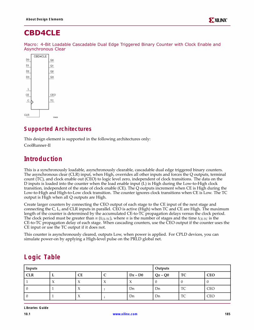
About Design Elements
CBD4CLEMacro: 4-Bit Loadable Cascadable Dual Edge Triggered Binary Counter with Clock Enable andAsynchronous Clear
Supported ArchitecturesThis design element is supported in the following architectures only:CoolRunner-II
IntroductionThis is a synchronously loadable, asynchronously clearable, cascadable dual edge triggered binary counters.The asynchronous clear (CLR) input, when High, overrides all other inputs and forces the Q outputs, terminalcount (TC), and clock enable out (CEO) to logic level zero, independent of clock transitions. The data on theD inputs is loaded into the counter when the load enable input (L) is High during the Low-to-High clocktransition, independent of the state of clock enable (CE). The Q outputs increment when CE is High during theLow-to-High and High-to-Low clock transition. The counter ignores clock transitions when CE is Low. The TCoutput is High when all Q outputs are High.
Create larger counters by connecting the CEO output of each stage to the CE input of the next stage andconnecting the C, L, and CLR inputs in parallel. CEO is active (High) when TC and CE are High. The maximumlength of the counter is determined by the accumulated CE-to-TC propagation delays versus the clock period.The clock period must be greater than n (tCE-TC), where n is the number of stages and the time tCE-TC is theCE-to-TC propagation delay of each stage. When cascading counters, use the CEO output if the counter uses theCE input or use the TC output if it does not.
This counter is asynchronously cleared, outputs Low, when power is applied. For CPLD devices, you cansimulate power-on by applying a High-level pulse on the PRLD global net.
Logic TableInputs Outputs
CLR L CE C Dz – D0 Qz – Q0 TC CEO
1 X X X X 0 0 0
0 1 X ↑ Dn Dn TC CEO
0 1 X ↓ Dn Dn TC CEO
Libraries Guide
10.1 www.xilinx.com 185

About Design Elements
Inputs Outputs
CLR L CE C Dz – D0 Qz – Q0 TC CEO
0 0 0 X X No change No change 0
0 0 1 ↑ X Inc TC CEO
0 0 1 ↓ X Inc TC CEO
z = bit width - 1
TC = Qz•Q(z-1)•Q(z-2)•...•Q0
CEO = TC•CE
Design Entry MethodThis design element is only for use in schematics.
For More Information• See the appropriate CPLD User Guide.
• See the appropriate CPLD Data Sheets.
Libraries Guide
186 www.xilinx.com 10.1

About Design Elements
CBD4CLED
Macro: 4-Bit Loadable Cascadable Bidirectional Dual Edge Triggered Binary Counter with ClockEnable and Asynchronous Clear
Supported Architectures
This design element is supported in the following architectures only:
CoolRunner-II
IntroductionThis design element is a synchronously loadable, asynchronously clearable, cascadable, bidirectional dual edgetriggered binary counter. The asynchronous clear (CLR) input, when High, overrides all other inputs andforces the Q outputs, terminal count (TC), and clock enable out (CEO) to logic level zero, independent of clocktransitions. The data on the D inputs is loaded into the counter when the load enable input (L) is High during theLow-to-High clock (C) transition, independent of the state of clock enable (CE). The Q outputs decrement whenCE is High and UP is Low during the Low-to-High and High-to-Low clock transition. The Q outputs incrementwhen CE and UP are High. The counter ignores clock transitions when CE is Low.
For counting up, the TC output is High when all Q outputs and UP are High. For counting down, the TCoutput is High when all Q outputs and UP are Low.
Create larger counters by connecting the CEO output of each stage to the CE input of the next stage andconnecting the C, UP, L, and CLR inputs in parallel. CEO is active (High) when TC and CE are High. Themaximum length of the counter is determined by the accumulated CE-to-TC propagation delays versus the clockperiod. The clock period must be greater than n (tCE-TC), where n is the number of stages and the time tCE-TC isthe CE-to-TC propagation delay of each stage. When cascading counters, use the CEO output if the counteruses the CE input or use the TC output if it does not.
See “CB2X1,” “CB4X1,” “CB8X1,” “CB16X1” for high-performance cascadable, bidirectional counters.
This counter is asynchronously cleared, outputs Low, when power is applied. For CPLD devices, you cansimulate power-on by applying a High-level pulse on the PRLD global net.
Libraries Guide
10.1 www.xilinx.com 187

About Design Elements
Logic TableInputs Outputs
CLR L CE C UP Dz – D0 Qz – Q0 TC CEO
1 X X X X X 0 0 0
0 1 X ↑ X Dn Dn TC CEO
0 1 X ↓ X Dn Dn TC CEO
0 0 0 X X X No change No change 0
0 0 1 ↑ 1 X Inc TC CEO
0 0 1 ↓ 1 X Inc TC CEO
0 0 1 ↑ 0 X Dec TC CEO
0 0 1 ↓ 0 X Dec TC CEO
z = bit width - 1
TC = (Qz•Q(z-1)•Q(z-2)•...•Q0•UP) + (Qz•Q(z-1)•Q(z-2)•...•Q0•UP)
CEO = TC•CE
Design Entry MethodThis design element is only for use in schematics.
For More Information• See the appropriate CPLD User Guide.
• See the appropriate CPLD Data Sheets.
Libraries Guide
188 www.xilinx.com 10.1

About Design Elements
CBD4RE
Macro: 4-Bit Cascadable Dual Edge Triggered Binary Counter with Clock Enable and SynchronousReset
Supported Architectures
This design element is supported in the following architectures only:
CoolRunner-II
IntroductionThis design element is a synchronous, resettable, cascadable dual edge triggered binary counter. The synchronousreset (R), when High, overrides all other inputs and forces the Q outputs, terminal count (TC), and clock enableout (CEO) to logic level zero during the Low-to-High or High-to-Low clock transition. The Q outputs incrementwhen the clock enable input (CE) is High during the Low-to-High and High-to-Low clock (C) transition. Thecounter ignores clock transitions when CE is Low. The TC output is High when both Q outputs are High.
Create larger counters by connecting the CEO output of each stage to the CE input of the next stage andconnecting the C and R inputs in parallel. CEO is active (High) when TC and CE are High. The maximum lengthof the counter is determined by the accumulated CE-to-TC propagation delays versus the clock period. Theclock period must be greater than n (tCE-TC), where n is the number of stages and the time tCE-TC is the CE-to-TCpropagation delay of each stage. When cascading counters, use the CEO output if the counter uses the CEinput or use the TC output if it does not.
This counter is asynchronously cleared, outputs Low, when power is applied. For CPLD devices, you cansimulate power-on by applying a High-level pulse on the PRLD global net.
Logic TableInputs Outputs
R CE C Qz-Q0 TC CEO
1 X ↑ 0 0 0
1 X ↓ 0 0 0
0 0 X No change No change 0
0 1 ↑ Inc TC CEO
Libraries Guide
10.1 www.xilinx.com 189
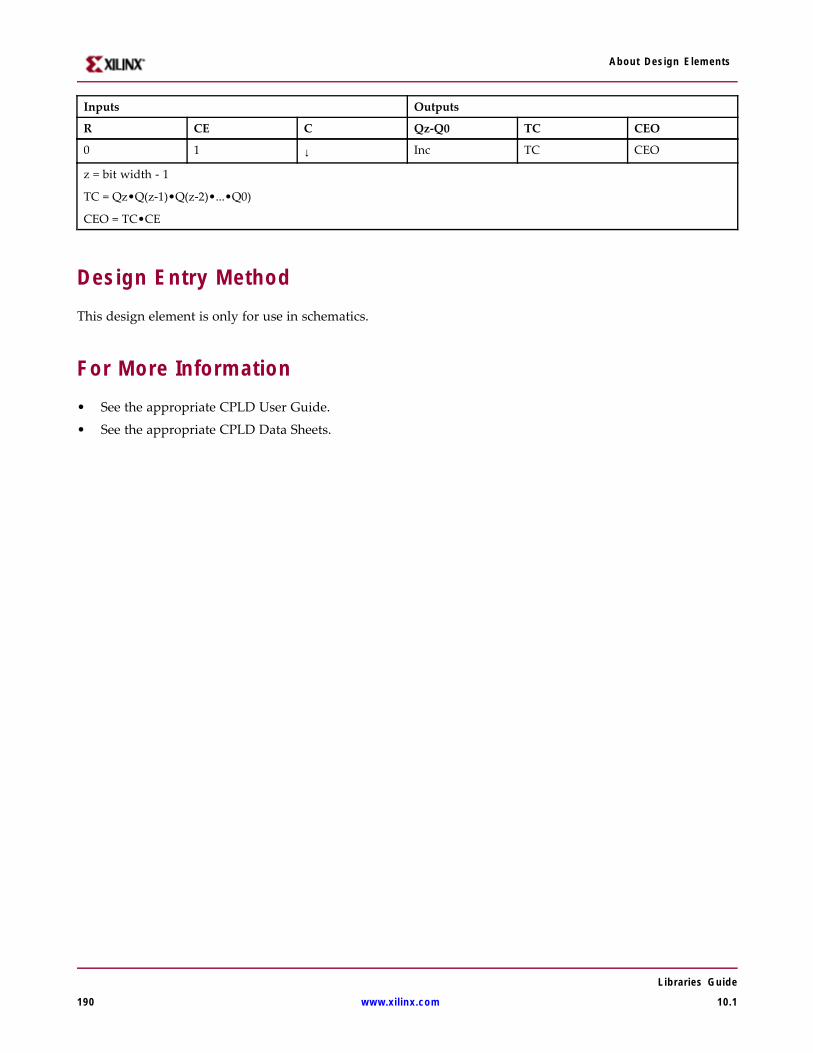
About Design Elements
Inputs Outputs
R CE C Qz-Q0 TC CEO
0 1 ↓ Inc TC CEO
z = bit width - 1
TC = Qz•Q(z-1)•Q(z-2)•...•Q0)
CEO = TC•CE
Design Entry MethodThis design element is only for use in schematics.
For More Information• See the appropriate CPLD User Guide.
• See the appropriate CPLD Data Sheets.
Libraries Guide
190 www.xilinx.com 10.1
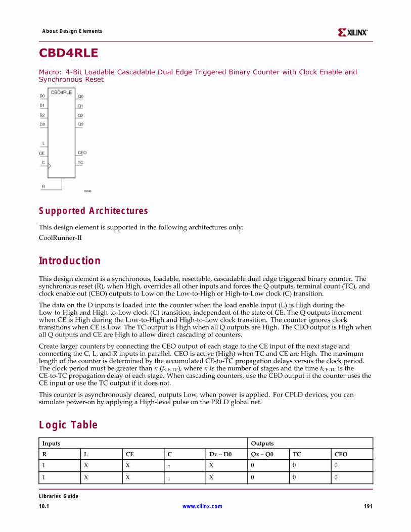
About Design Elements
CBD4RLEMacro: 4-Bit Loadable Cascadable Dual Edge Triggered Binary Counter with Clock Enable andSynchronous Reset
Supported ArchitecturesThis design element is supported in the following architectures only:CoolRunner-II
IntroductionThis design element is a synchronous, loadable, resettable, cascadable dual edge triggered binary counter. Thesynchronous reset (R), when High, overrides all other inputs and forces the Q outputs, terminal count (TC), andclock enable out (CEO) outputs to Low on the Low-to-High or High-to-Low clock (C) transition.
The data on the D inputs is loaded into the counter when the load enable input (L) is High during theLow-to-High and High-to-Low clock (C) transition, independent of the state of CE. The Q outputs incrementwhen CE is High during the Low-to-High and High-to-Low clock transition. The counter ignores clocktransitions when CE is Low. The TC output is High when all Q outputs are High. The CEO output is High whenall Q outputs and CE are High to allow direct cascading of counters.
Create larger counters by connecting the CEO output of each stage to the CE input of the next stage andconnecting the C, L, and R inputs in parallel. CEO is active (High) when TC and CE are High. The maximumlength of the counter is determined by the accumulated CE-to-TC propagation delays versus the clock period.The clock period must be greater than n (tCE-TC), where n is the number of stages and the time tCE-TC is theCE-to-TC propagation delay of each stage. When cascading counters, use the CEO output if the counter uses theCE input or use the TC output if it does not.
This counter is asynchronously cleared, outputs Low, when power is applied. For CPLD devices, you cansimulate power-on by applying a High-level pulse on the PRLD global net.
Logic TableInputs Outputs
R L CE C Dz – D0 Qz – Q0 TC CEO
1 X X ↑ X 0 0 0
1 X X ↓ X 0 0 0
Libraries Guide
10.1 www.xilinx.com 191
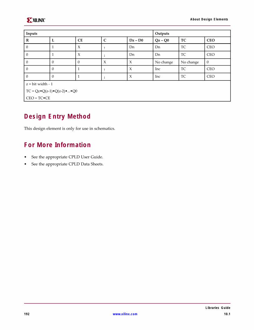
About Design Elements
Inputs Outputs
R L CE C Dz – D0 Qz – Q0 TC CEO
0 1 X ↑ Dn Dn TC CEO
0 1 X ↓ Dn Dn TC CEO
0 0 0 X X No change No change 0
0 0 1 ↑ X Inc TC CEO
0 0 1 ↓ X Inc TC CEO
z = bit width - 1
TC = Qz•Q(z-1)•Q(z-2)•...•Q0
CEO = TC•CE
Design Entry MethodThis design element is only for use in schematics.
For More Information• See the appropriate CPLD User Guide.
• See the appropriate CPLD Data Sheets.
Libraries Guide
192 www.xilinx.com 10.1

About Design Elements
CBD4X1
Macro: 4-Bit Loadable Cascadable Bidirectional Dual Edge Triggered Binary Counter with ClockEnable and Asynchronous Clear
Supported Architectures
This design element is supported in the following architectures only:
CoolRunner-II
IntroductionThis design element is a synchronously loadable, asynchronously clearable, bidirectional dual edge triggeredbinary counters. It has separate count-enable inputs and synchronous terminal-count outputs for up and downdirections to support high speed cascading.
The asynchronous clear (CLR) is the highest priority input. When CLR is High, all other inputs are ignored; dataoutputs (Q) go to logic level zero, terminal count outputs TCU and TCD go to zero and one, respectively, clockenable outputs CEOU and CEOD go to Low and High, respectively, independent of clock transitions. The dataon the D inputs loads into the counter on the Low-to-High and High-to-Low clock (C) transition when the loadenable input (L) is High, independent of the CE inputs.
The Q outputs increment when CEU is High, provided CLR and L are Low, during the Low-to-High andHigh-to-Low clock transition. The Q outputs decrement when CED is High, provided CLR and L are Low.The counter ignores clock transitions when CEU and CED are Low. Both CEU and CED should not be Highduring the same clock transition; the CEOU and CEOD outputs might not function properly for cascading whenCEU and CED are both High.
For counting up, the CEOU output is High when all Q outputs and CEU are High. For counting down, theCEOD output is High when all Q outputs are Low and CED is High. To cascade counters, the CEOU and CEODoutputs of each counter are connected directly to the CEU and CED inputs, respectively, of the next stage. Theclock, L, and CLR inputs are connected in parallel.
The maximum clocking frequency of these counters is unaffected by the number of cascaded stages for allcounting and loading functions. The TCU terminal count output is High when all Q outputs are High, regardlessof CEU. The TCD output is High when all Q outputs are Low, regardless of CED.
Libraries Guide
10.1 www.xilinx.com 193
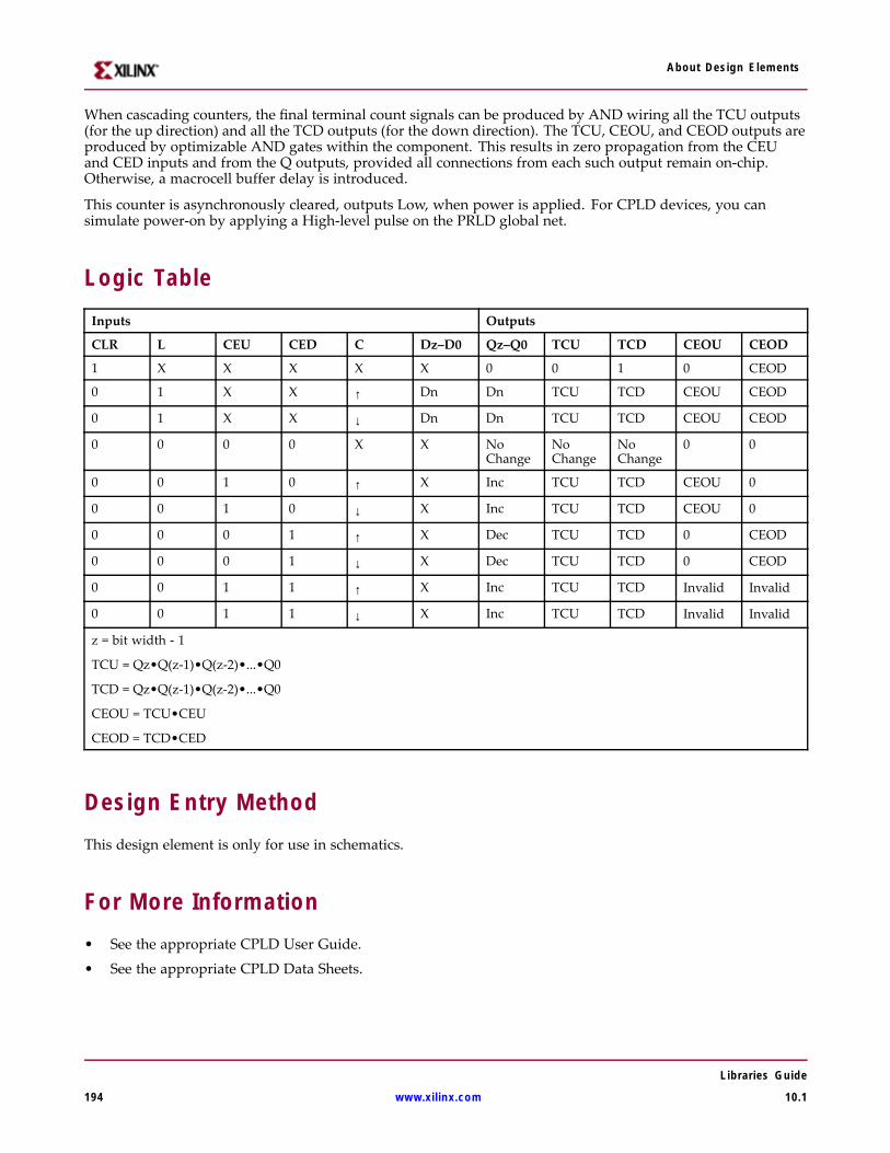
About Design Elements
When cascading counters, the final terminal count signals can be produced by AND wiring all the TCU outputs(for the up direction) and all the TCD outputs (for the down direction). The TCU, CEOU, and CEOD outputs areproduced by optimizable AND gates within the component. This results in zero propagation from the CEUand CED inputs and from the Q outputs, provided all connections from each such output remain on-chip.Otherwise, a macrocell buffer delay is introduced.
This counter is asynchronously cleared, outputs Low, when power is applied. For CPLD devices, you cansimulate power-on by applying a High-level pulse on the PRLD global net.
Logic TableInputs Outputs
CLR L CEU CED C Dz–D0 Qz–Q0 TCU TCD CEOU CEOD
1 X X X X X 0 0 1 0 CEOD
0 1 X X ↑ Dn Dn TCU TCD CEOU CEOD
0 1 X X ↓ Dn Dn TCU TCD CEOU CEOD
0 0 0 0 X X NoChange
NoChange
NoChange
0 0
0 0 1 0 ↑ X Inc TCU TCD CEOU 0
0 0 1 0 ↓ X Inc TCU TCD CEOU 0
0 0 0 1 ↑ X Dec TCU TCD 0 CEOD
0 0 0 1 ↓ X Dec TCU TCD 0 CEOD
0 0 1 1 ↑ X Inc TCU TCD Invalid Invalid
0 0 1 1 ↓ X Inc TCU TCD Invalid Invalid
z = bit width - 1
TCU = Qz•Q(z-1)•Q(z-2)•...•Q0
TCD = Qz•Q(z-1)•Q(z-2)•...•Q0
CEOU = TCU•CEU
CEOD = TCD•CED
Design Entry MethodThis design element is only for use in schematics.
For More Information• See the appropriate CPLD User Guide.
• See the appropriate CPLD Data Sheets.
Libraries Guide
194 www.xilinx.com 10.1
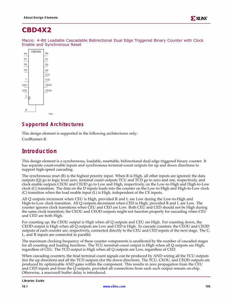
About Design Elements
CBD4X2Macro: 4-Bit Loadable Cascadable Bidirectional Dual Edge Triggered Binary Counter with ClockEnable and Synchronous Reset
Supported ArchitecturesThis design element is supported in the following architectures only:CoolRunner-II
IntroductionThis design element is a synchronous, loadable, resettable, bidirectional dual edge triggered binary counter. Ithas separate count-enable inputs and synchronous terminal-count outputs for up and down directions tosupport high-speed cascading.
The synchronous reset (R) is the highest priority input. When R is High, all other inputs are ignored; the dataoutputs (Q) go to logic level zero, terminal count outputs TCU and TCD go to zero and one, respectively, andclock enable outputs CEOU and CEOD go to Low and High, respectively, on the Low-to-High and High-to-Lowclock (C) transition. The data on the D inputs loads into the counter on the Low-to-High and High-to-Low clock(C) transition when the load enable input (L) is High, independent of the CE inputs.
All Q outputs increment when CEU is High, provided R and L are Low during the Low-to-High andHigh-to-Low clock transition. All Q outputs decrement when CED is High, provided R and L are Low. Thecounter ignores clock transitions when CEU and CED are Low. Both CEU and CED should not be High duringthe same clock transition; the CEOU and CEOD outputs might not function properly for cascading when CEUand CED are both High.
For counting up, the CEOU output is High when all Q outputs and CEU are High. For counting down, theCEOD output is High when all Q outputs are Low and CED is High. To cascade counters, the CEOU and CEODoutputs of each counter are, respectively, connected directly to the CEU and CED inputs of the next stage. The C,L, and R inputs are connected in parallel.
The maximum clocking frequency of these counter components is unaffected by the number of cascaded stagesfor all counting and loading functions. The TCU terminal count output is High when all Q outputs are High,regardless of CEU. The TCD output is High when all Q outputs are Low, regardless of CED.
When cascading counters, the final terminal count signals can be produced by AND wiring all the TCU outputs(for the up direction) and all the TCD outputs (for the down direction). The TCU, CEOU, and CEOD outputs areproduced by optimizable AND gates within the component. This results in zero propagation from the CEUand CED inputs and from the Q outputs, provided all connections from each such output remain on-chip.Otherwise, a macrocell buffer delay is introduced.
Libraries Guide
10.1 www.xilinx.com 195

About Design Elements
This counter is asynchronously cleared, outputs Low, when power is applied. For CPLD devices, you cansimulate power-on by applying a High-level pulse on the PRLD global net.
Logic TableInputs Outputs
R L CEU CED C Dz – D0 Qz – Q0 TCU TCD CEOU CEOD
1 X X X ↑ X 0 0 1 0 CEOD
1 X X X ↓ X 0 0 1 0 CEOD
0 1 X X ↑ Dn Dn TCU TCD CEOU CEOD
0 1 X X ↓ Dn Dn TCU TCD CEOU CEOD
0 0 0 0 X X NoChange NoChange
NoChange
0 0
0 0 1 0 ↑ X Inc TCU TCD CEOU 0
0 0 1 0 ↓ X Inc TCU TCD CEOU 0
0 0 0 1 ↑ X Dec TCU TCD 0 CEOD
0 0 0 1 ↓ X Dec TCU TCD 0 CEOD
0 0 1 1 ↑ X Inc TCU TCD Invalid Invalid
0 0 1 1 ↓ X Inc TCU TCD Invalid Invalid
z = bit width - 1
TCU = Qz•Q(z-1)•Q(z-2)•...•Q0
TCD = Qz•Q(z-1)•Q(z-2)•...•Q0
CEOU = TCU•CEU
CEOD = TCD•CED
Design Entry MethodThis design element is only for use in schematics.
For More Information• See the appropriate CPLD User Guide.
• See the appropriate CPLD Data Sheets.
Libraries Guide
196 www.xilinx.com 10.1

About Design Elements
CBD8CE
Macro: 8-Bit Cascadable Dual Edge Triggered Binary Counter with Clock Enable and AsynchronousClear
Supported Architectures
This design element is supported in the following architectures only:
CoolRunner-II
IntroductionThis element is an asynchronously clearable, cascadable dual edge triggered binary counter. The asynchronousclear (CLR) input, when High, overrides all other inputs and forces the Q outputs, terminal count (TC), and clockenable out (CEO) to logic level zero, independent of clock transitions. The Q outputs increment when the clockenable input (CE) is High during the Low-to-High and High-to-Low clock (C) transition. The counter ignoresclock transitions when CE is Low. The TC output is High when all Q outputs are High.
Create larger counters by connecting the CEO output of each stage to the CE input of the next stage andconnecting the C and CLR inputs in parallel. CEO is active (High) when TC and CE are High. The maximumlength of the counter is determined by the accumulated CE-to-TC propagation delays versus the clock period.The clock period must be greater than n (tCE-TC), where n is the number of stages and the time tCE-TC is theCE-to-TC propagation delay of each stage. When cascading counters, use the CEO output if the counter uses theCE input or use the TC output if it does not.
This counter is asynchronously cleared, outputs Low, when power is applied. For CPLD devices, you cansimulate power-on by applying a High-level pulse on the PRLD global net.
Logic TableInputs Outputs
CLR CE C Qz – Q0 TC CEO
1 X X 0 0 0
0 0 X No change No change 0
0 1 ↑ Inc TC CEO
0 1 ↓ Inc TC CEO
z = bit width - 1
TC = Qz•Q(z-1)•Q(z-2)•...•Q0
CEO = TC•CE
Libraries Guide
10.1 www.xilinx.com 197

About Design Elements
Design Entry MethodThis design element is only for use in schematics.
For More Information• See the appropriate CPLD User Guide.
• See the appropriate CPLD Data Sheets.
Libraries Guide
198 www.xilinx.com 10.1
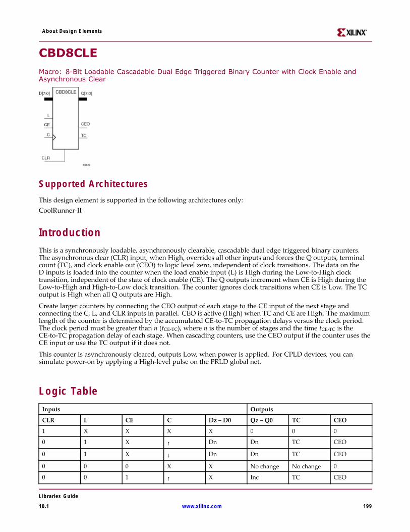
About Design Elements
CBD8CLEMacro: 8-Bit Loadable Cascadable Dual Edge Triggered Binary Counter with Clock Enable andAsynchronous Clear
Supported ArchitecturesThis design element is supported in the following architectures only:CoolRunner-II
IntroductionThis is a synchronously loadable, asynchronously clearable, cascadable dual edge triggered binary counters.The asynchronous clear (CLR) input, when High, overrides all other inputs and forces the Q outputs, terminalcount (TC), and clock enable out (CEO) to logic level zero, independent of clock transitions. The data on theD inputs is loaded into the counter when the load enable input (L) is High during the Low-to-High clocktransition, independent of the state of clock enable (CE). The Q outputs increment when CE is High during theLow-to-High and High-to-Low clock transition. The counter ignores clock transitions when CE is Low. The TCoutput is High when all Q outputs are High.
Create larger counters by connecting the CEO output of each stage to the CE input of the next stage andconnecting the C, L, and CLR inputs in parallel. CEO is active (High) when TC and CE are High. The maximumlength of the counter is determined by the accumulated CE-to-TC propagation delays versus the clock period.The clock period must be greater than n (tCE-TC), where n is the number of stages and the time tCE-TC is theCE-to-TC propagation delay of each stage. When cascading counters, use the CEO output if the counter uses theCE input or use the TC output if it does not.
This counter is asynchronously cleared, outputs Low, when power is applied. For CPLD devices, you cansimulate power-on by applying a High-level pulse on the PRLD global net.
Logic TableInputs Outputs
CLR L CE C Dz – D0 Qz – Q0 TC CEO
1 X X X X 0 0 0
0 1 X ↑ Dn Dn TC CEO
0 1 X ↓ Dn Dn TC CEO
0 0 0 X X No change No change 0
0 0 1 ↑ X Inc TC CEO
Libraries Guide
10.1 www.xilinx.com 199

About Design Elements
Inputs Outputs
CLR L CE C Dz – D0 Qz – Q0 TC CEO
0 0 1 ↓ X Inc TC CEO
z = bit width - 1
TC = Qz•Q(z-1)•Q(z-2)•...•Q0
CEO = TC•CE
Design Entry MethodThis design element is only for use in schematics.
For More Information• See the appropriate CPLD User Guide.
• See the appropriate CPLD Data Sheets.
Libraries Guide
200 www.xilinx.com 10.1
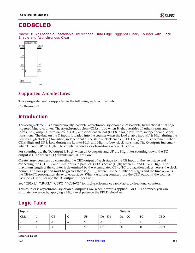
About Design Elements
CBD8CLEDMacro: 8-Bit Loadable Cascadable Bidirectional Dual Edge Triggered Binary Counter with ClockEnable and Asynchronous Clear
Supported ArchitecturesThis design element is supported in the following architectures only:CoolRunner-II
IntroductionThis design element is a synchronously loadable, asynchronously clearable, cascadable, bidirectional dual edgetriggered binary counter. The asynchronous clear (CLR) input, when High, overrides all other inputs andforces the Q outputs, terminal count (TC), and clock enable out (CEO) to logic level zero, independent of clocktransitions. The data on the D inputs is loaded into the counter when the load enable input (L) is High during theLow-to-High clock (C) transition, independent of the state of clock enable (CE). The Q outputs decrement whenCE is High and UP is Low during the Low-to-High and High-to-Low clock transition. The Q outputs incrementwhen CE and UP are High. The counter ignores clock transitions when CE is Low.
For counting up, the TC output is High when all Q outputs and UP are High. For counting down, the TCoutput is High when all Q outputs and UP are Low.
Create larger counters by connecting the CEO output of each stage to the CE input of the next stage andconnecting the C, UP, L, and CLR inputs in parallel. CEO is active (High) when TC and CE are High. Themaximum length of the counter is determined by the accumulated CE-to-TC propagation delays versus the clockperiod. The clock period must be greater than n (tCE-TC), where n is the number of stages and the time tCE-TC isthe CE-to-TC propagation delay of each stage. When cascading counters, use the CEO output if the counteruses the CE input or use the TC output if it does not.
See “CB2X1,” “CB4X1,” “CB8X1,” “CB16X1” for high-performance cascadable, bidirectional counters.
This counter is asynchronously cleared, outputs Low, when power is applied. For CPLD devices, you cansimulate power-on by applying a High-level pulse on the PRLD global net.
Logic TableInputs Outputs
CLR L CE C UP Dz – D0 Qz – Q0 TC CEO
1 X X X X X 0 0 0
0 1 X ↑ X Dn Dn TC CEO
Libraries Guide
10.1 www.xilinx.com 201

About Design Elements
Inputs Outputs
CLR L CE C UP Dz – D0 Qz – Q0 TC CEO
0 1 X ↓ X Dn Dn TC CEO
0 0 0 X X X No change No change 0
0 0 1 ↑ 1 X Inc TC CEO
0 0 1 ↓ 1 X Inc TC CEO
0 0 1 ↑ 0 X Dec TC CEO
0 0 1 ↓ 0 X Dec TC CEO
z = bit width - 1
TC = (Qz•Q(z-1)•Q(z-2)•...•Q0•UP) + (Qz•Q(z-1)•Q(z-2)•...•Q0•UP)
CEO = TC•CE
Design Entry MethodThis design element is only for use in schematics.
For More Information• See the appropriate CPLD User Guide.
• See the appropriate CPLD Data Sheets.
Libraries Guide
202 www.xilinx.com 10.1

About Design Elements
CBD8RE
Macro: 8-Bit Cascadable Dual Edge Triggered Binary Counter with Clock Enable and SynchronousReset
Supported ArchitecturesThis design element is supported in the following architectures only:CoolRunner-II
IntroductionThis design element is a synchronous, resettable, cascadable dual edge triggered binary counter. The synchronousreset (R), when High, overrides all other inputs and forces the Q outputs, terminal count (TC), and clock enableout (CEO) to logic level zero during the Low-to-High or High-to-Low clock transition. The Q outputs incrementwhen the clock enable input (CE) is High during the Low-to-High and High-to-Low clock (C) transition. Thecounter ignores clock transitions when CE is Low. The TC output is High when both Q outputs are High.
Create larger counters by connecting the CEO output of each stage to the CE input of the next stage andconnecting the C and R inputs in parallel. CEO is active (High) when TC and CE are High. The maximum lengthof the counter is determined by the accumulated CE-to-TC propagation delays versus the clock period. Theclock period must be greater than n (tCE-TC), where n is the number of stages and the time tCE-TC is the CE-to-TCpropagation delay of each stage. When cascading counters, use the CEO output if the counter uses the CEinput or use the TC output if it does not.
This counter is asynchronously cleared, outputs Low, when power is applied. For CPLD devices, you cansimulate power-on by applying a High-level pulse on the PRLD global net.
Logic TableInputs Outputs
R CE C Qz-Q0 TC CEO
1 X ↑ 0 0 0
1 X ↓ 0 0 0
0 0 X No change No change 0
0 1 ↑ Inc TC CEO
0 1 ↓ Inc TC CEO
z = bit width - 1
TC = Qz•Q(z-1)•Q(z-2)•...•Q0)
CEO = TC•CE
Libraries Guide
10.1 www.xilinx.com 203

About Design Elements
Design Entry MethodThis design element is only for use in schematics.
For More Information• See the appropriate CPLD User Guide.
• See the appropriate CPLD Data Sheets.
Libraries Guide
204 www.xilinx.com 10.1

About Design Elements
CBD8RLEMacro: 8-Bit Loadable Cascadable Dual Edge Triggered Binary Counter with Clock Enable andSynchronous Reset
Supported ArchitecturesThis design element is supported in the following architectures only:CoolRunner-II
IntroductionThis design element is a synchronous, loadable, resettable, cascadable dual edge triggered binary counter. Thesynchronous reset (R), when High, overrides all other inputs and forces the Q outputs, terminal count (TC), andclock enable out (CEO) outputs to Low on the Low-to-High or High-to-Low clock (C) transition.
The data on the D inputs is loaded into the counter when the load enable input (L) is High during theLow-to-High and High-to-Low clock (C) transition, independent of the state of CE. The Q outputs incrementwhen CE is High during the Low-to-High and High-to-Low clock transition. The counter ignores clocktransitions when CE is Low. The TC output is High when all Q outputs are High. The CEO output is High whenall Q outputs and CE are High to allow direct cascading of counters.
Create larger counters by connecting the CEO output of each stage to the CE input of the next stage andconnecting the C, L, and R inputs in parallel. CEO is active (High) when TC and CE are High. The maximumlength of the counter is determined by the accumulated CE-to-TC propagation delays versus the clock period.The clock period must be greater than n (tCE-TC), where n is the number of stages and the time tCE-TC is theCE-to-TC propagation delay of each stage. When cascading counters, use the CEO output if the counter uses theCE input or use the TC output if it does not.
This counter is asynchronously cleared, outputs Low, when power is applied. For CPLD devices, you cansimulate power-on by applying a High-level pulse on the PRLD global net.
Logic TableInputs Outputs
R L CE C Dz – D0 Qz – Q0 TC CEO
1 X X ↑ X 0 0 0
1 X X ↓ X 0 0 0
0 1 X ↑ Dn Dn TC CEO
0 1 X ↓ Dn Dn TC CEO
Libraries Guide
10.1 www.xilinx.com 205

About Design Elements
Inputs Outputs
R L CE C Dz – D0 Qz – Q0 TC CEO
0 0 0 X X No change No change 0
0 0 1 ↑ X Inc TC CEO
0 0 1 ↓ X Inc TC CEO
z = bit width - 1
TC = Qz•Q(z-1)•Q(z-2)•...•Q0
CEO = TC•CE
Design Entry MethodThis design element is only for use in schematics.
For More Information• See the appropriate CPLD User Guide.
• See the appropriate CPLD Data Sheets.
Libraries Guide
206 www.xilinx.com 10.1

About Design Elements
CBD8X1Macro: 8-Bit Loadable Cascadable Bidirectional Dual Edge Triggered Binary Counter with ClockEnable and Asynchronous Clear
Supported ArchitecturesThis design element is supported in the following architectures only:CoolRunner-II
IntroductionThis design element is a synchronously loadable, asynchronously clearable, bidirectional dual edge triggeredbinary counters. It has separate count-enable inputs and synchronous terminal-count outputs for up and downdirections to support high speed cascading.
The asynchronous clear (CLR) is the highest priority input. When CLR is High, all other inputs are ignored; dataoutputs (Q) go to logic level zero, terminal count outputs TCU and TCD go to zero and one, respectively, clockenable outputs CEOU and CEOD go to Low and High, respectively, independent of clock transitions. The dataon the D inputs loads into the counter on the Low-to-High and High-to-Low clock (C) transition when the loadenable input (L) is High, independent of the CE inputs.
The Q outputs increment when CEU is High, provided CLR and L are Low, during the Low-to-High andHigh-to-Low clock transition. The Q outputs decrement when CED is High, provided CLR and L are Low.The counter ignores clock transitions when CEU and CED are Low. Both CEU and CED should not be Highduring the same clock transition; the CEOU and CEOD outputs might not function properly for cascading whenCEU and CED are both High.
For counting up, the CEOU output is High when all Q outputs and CEU are High. For counting down, theCEOD output is High when all Q outputs are Low and CED is High. To cascade counters, the CEOU and CEODoutputs of each counter are connected directly to the CEU and CED inputs, respectively, of the next stage. Theclock, L, and CLR inputs are connected in parallel.
The maximum clocking frequency of these counters is unaffected by the number of cascaded stages for allcounting and loading functions. The TCU terminal count output is High when all Q outputs are High, regardlessof CEU. The TCD output is High when all Q outputs are Low, regardless of CED.
When cascading counters, the final terminal count signals can be produced by AND wiring all the TCU outputs(for the up direction) and all the TCD outputs (for the down direction). The TCU, CEOU, and CEOD outputs areproduced by optimizable AND gates within the component. This results in zero propagation from the CEUand CED inputs and from the Q outputs, provided all connections from each such output remain on-chip.Otherwise, a macrocell buffer delay is introduced.
This counter is asynchronously cleared, outputs Low, when power is applied. For CPLD devices, you cansimulate power-on by applying a High-level pulse on the PRLD global net.
Libraries Guide
10.1 www.xilinx.com 207
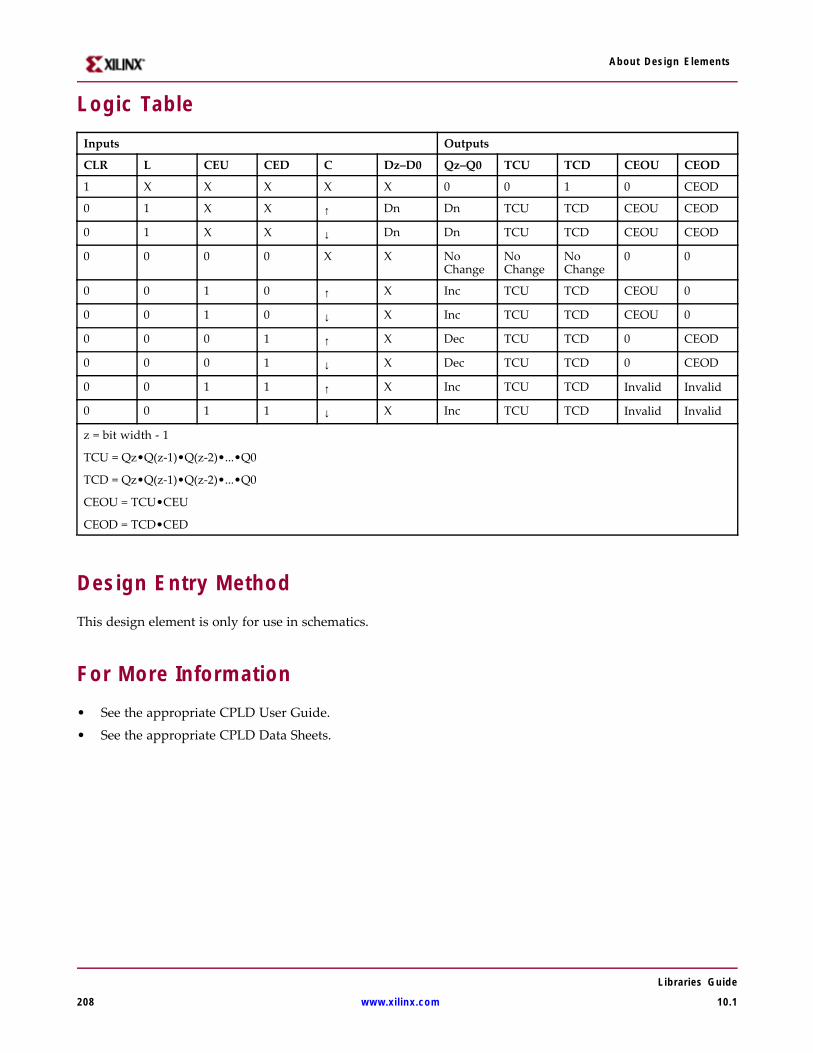
About Design Elements
Logic TableInputs Outputs
CLR L CEU CED C Dz–D0 Qz–Q0 TCU TCD CEOU CEOD
1 X X X X X 0 0 1 0 CEOD
0 1 X X ↑ Dn Dn TCU TCD CEOU CEOD
0 1 X X ↓ Dn Dn TCU TCD CEOU CEOD
0 0 0 0 X X NoChange
NoChange
NoChange
0 0
0 0 1 0 ↑ X Inc TCU TCD CEOU 0
0 0 1 0 ↓ X Inc TCU TCD CEOU 0
0 0 0 1 ↑ X Dec TCU TCD 0 CEOD
0 0 0 1 ↓ X Dec TCU TCD 0 CEOD
0 0 1 1 ↑ X Inc TCU TCD Invalid Invalid
0 0 1 1 ↓ X Inc TCU TCD Invalid Invalid
z = bit width - 1
TCU = Qz•Q(z-1)•Q(z-2)•...•Q0
TCD = Qz•Q(z-1)•Q(z-2)•...•Q0
CEOU = TCU•CEU
CEOD = TCD•CED
Design Entry MethodThis design element is only for use in schematics.
For More Information• See the appropriate CPLD User Guide.
• See the appropriate CPLD Data Sheets.
Libraries Guide
208 www.xilinx.com 10.1

About Design Elements
CBD8X2
Macro: 8-Bit Loadable Cascadable Bidirectional Dual Edge Triggered Binary Counter with ClockEnable and Synchronous Reset
Supported ArchitecturesThis design element is supported in the following architectures only:CoolRunner-II
IntroductionThis design element is a synchronous, loadable, resettable, bidirectional dual edge triggered binary counter. Ithas separate count-enable inputs and synchronous terminal-count outputs for up and down directions tosupport high-speed cascading.
The synchronous reset (R) is the highest priority input. When R is High, all other inputs are ignored; the dataoutputs (Q) go to logic level zero, terminal count outputs TCU and TCD go to zero and one, respectively, andclock enable outputs CEOU and CEOD go to Low and High, respectively, on the Low-to-High and High-to-Lowclock (C) transition. The data on the D inputs loads into the counter on the Low-to-High and High-to-Low clock(C) transition when the load enable input (L) is High, independent of the CE inputs.
All Q outputs increment when CEU is High, provided R and L are Low during the Low-to-High andHigh-to-Low clock transition. All Q outputs decrement when CED is High, provided R and L are Low. Thecounter ignores clock transitions when CEU and CED are Low. Both CEU and CED should not be High duringthe same clock transition; the CEOU and CEOD outputs might not function properly for cascading when CEUand CED are both High.
For counting up, the CEOU output is High when all Q outputs and CEU are High. For counting down, theCEOD output is High when all Q outputs are Low and CED is High. To cascade counters, the CEOU and CEODoutputs of each counter are, respectively, connected directly to the CEU and CED inputs of the next stage. The C,L, and R inputs are connected in parallel.
The maximum clocking frequency of these counter components is unaffected by the number of cascaded stagesfor all counting and loading functions. The TCU terminal count output is High when all Q outputs are High,regardless of CEU. The TCD output is High when all Q outputs are Low, regardless of CED.
When cascading counters, the final terminal count signals can be produced by AND wiring all the TCU outputs(for the up direction) and all the TCD outputs (for the down direction). The TCU, CEOU, and CEOD outputs areproduced by optimizable AND gates within the component. This results in zero propagation from the CEUand CED inputs and from the Q outputs, provided all connections from each such output remain on-chip.Otherwise, a macrocell buffer delay is introduced.
This counter is asynchronously cleared, outputs Low, when power is applied. For CPLD devices, you cansimulate power-on by applying a High-level pulse on the PRLD global net.
Libraries Guide
10.1 www.xilinx.com 209

About Design Elements
Logic TableInputs Outputs
R L CEU CED C Dz – D0 Qz – Q0 TCU TCD CEOU CEOD
1 X X X ↑ X 0 0 1 0 CEOD
1 X X X ↓ X 0 0 1 0 CEOD
0 1 X X ↑ Dn Dn TCU TCD CEOU CEOD
0 1 X X ↓ Dn Dn TCU TCD CEOU CEOD
0 0 0 0 X X NoChange NoChange
NoChange
0 0
0 0 1 0 ↑ X Inc TCU TCD CEOU 0
0 0 1 0 ↓ X Inc TCU TCD CEOU 0
0 0 0 1 ↑ X Dec TCU TCD 0 CEOD
0 0 0 1 ↓ X Dec TCU TCD 0 CEOD
0 0 1 1 ↑ X Inc TCU TCD Invalid Invalid
0 0 1 1 ↓ X Inc TCU TCD Invalid Invalid
z = bit width - 1
TCU = Qz•Q(z-1)•Q(z-2)•...•Q0
TCD = Qz•Q(z-1)•Q(z-2)•...•Q0
CEOU = TCU•CEU
CEOD = TCD•CED
Design Entry MethodThis design element is only for use in schematics.
For More Information• See the appropriate CPLD User Guide.
• See the appropriate CPLD Data Sheets.
Libraries Guide
210 www.xilinx.com 10.1

About Design Elements
CD4CEMacro: 4-Bit Cascadable BCD Counter with Clock Enable and Asynchronous Clear
Supported ArchitecturesThis design element is supported in the following architectures only:• XC9500XL• CoolRunner XPLA3• CoolRunner-II
IntroductionCD4CE is a 4-bit (stage), asynchronous clearable, cascadable binary-coded-decimal (BCD) counter. Theasynchronous clear input (CLR) is the highest priority input. When CLR is High, all other inputs are ignored;the Q outputs, terminal count (TC), and clock enable out (CEO) go to logic level zero, independent of clocktransitions. The Q outputs increment when clock enable (CE) is High during the Low-to-High clock (C)transition. The counter ignores clock transitions when CE is Low. The TC output is High when Q3 and Q0 areHigh and Q2 and Q1 are Low.
The counter recovers from any of six possible illegal states and returns to a normal count sequence within twoclock cycles for Xilinx® devices, as shown in the following state diagram:
Create larger counters by connecting the CEO output of each stage to the CE input of the next stage andconnecting the C and CLR inputs in parallel. CEO is active (High) when TC and CE are High. The maximumlength of the counter is determined by the accumulated CE-to-TC propagation delays versus the clock period.The clock period must be greater than n (tCE-TC), where n is the number of stages and the time tCE-TC is theCE-to-TC propagation delay of each stage. When cascading counters, use the CEO output if the counter uses theCE input or use the TC output if it does not.
This counter is asynchronously cleared, outputs Low, when power is applied. For CPLD devices, you cansimulate power-on by applying a High-level pulse on the PRLD global net.
Libraries Guide
10.1 www.xilinx.com 211

About Design Elements
Logic TableInputs Outputs
CLR CE C Q3 Q2 Q1 Q0 TC CEO
1 X X 0 0 0 0 0 0
0 1 ↑ Inc Inc Inc Inc TC CEO
0 0 X No Change No Change No Change No Change TC 0
0 1 X 1 0 0 1 1 1
TC = Q3•!Q2•!Q1•Q0
CEO = TC•CE
Design Entry MethodThis design element is only for use in schematics.
For More Information• See the appropriate CPLD User Guide.
• See the appropriate CPLD Data Sheets.
Libraries Guide
212 www.xilinx.com 10.1
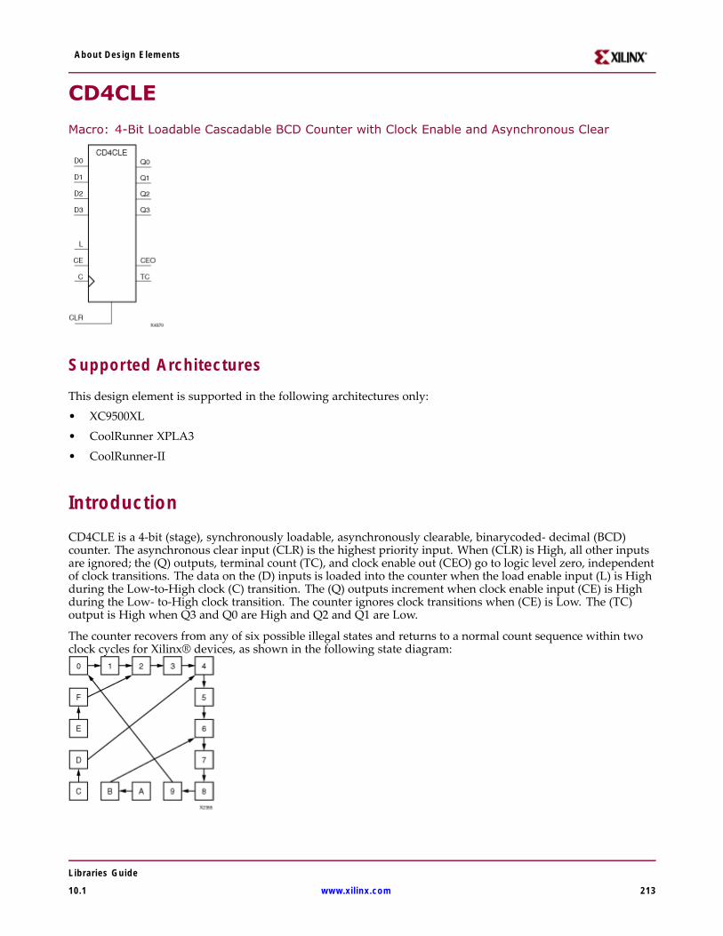
About Design Elements
CD4CLE
Macro: 4-Bit Loadable Cascadable BCD Counter with Clock Enable and Asynchronous Clear
Supported Architectures
This design element is supported in the following architectures only:
• XC9500XL
• CoolRunner XPLA3
• CoolRunner-II
IntroductionCD4CLE is a 4-bit (stage), synchronously loadable, asynchronously clearable, binarycoded- decimal (BCD)counter. The asynchronous clear input (CLR) is the highest priority input. When (CLR) is High, all other inputsare ignored; the (Q) outputs, terminal count (TC), and clock enable out (CEO) go to logic level zero, independentof clock transitions. The data on the (D) inputs is loaded into the counter when the load enable input (L) is Highduring the Low-to-High clock (C) transition. The (Q) outputs increment when clock enable input (CE) is Highduring the Low- to-High clock transition. The counter ignores clock transitions when (CE) is Low. The (TC)output is High when Q3 and Q0 are High and Q2 and Q1 are Low.
The counter recovers from any of six possible illegal states and returns to a normal count sequence within twoclock cycles for Xilinx® devices, as shown in the following state diagram:
Libraries Guide
10.1 www.xilinx.com 213

About Design Elements
Create larger counters by connecting the CEO output of each stage to the CE input of the next stage andconnecting the C, L, and CLR inputs in parallel. CEO is active (High) when TC and CE are High. The maximumlength of the counter is determined by the accumulated CE-to-TC propagation delays versus the clock period.The clock period must be greater than n (tCE-TC), where n is the number of stages and the time tCE-TC is theCE-to-TC propagation delay of each stage. When cascading counters, use the CEO output if the counter uses theCE input or use the TC output if it does not.
This counter is asynchronously cleared, outputs Low, when power is applied. For CPLD devices, you cansimulate power-on by applying a High-level pulse on the PRLD global net.
Logic TableInputs Outputs
CLR L CE D3 – D0 C Q3 Q2 Q1 Q0 TC CEO
1 X X X X 0 0 0 0 0 0
0 1 X D3 – D0 ↑ D3 D2 D1 D0 TC CEO
0 0 1 X ↑ Inc Inc Inc Inc TC CEO
0 0 0 X X NoChange
NoChange
NoChange
NoChange
TC 0
0 0 1 X X 1 0 0 1 1 1
TC = Q3•!Q2•!Q1•Q0
CEO = TC•CE
Design Entry MethodThis design element is only for use in schematics.
For More Information• See the appropriate CPLD User Guide.
• See the appropriate CPLD Data Sheets.
Libraries Guide
214 www.xilinx.com 10.1

About Design Elements
CD4REMacro: 4-Bit Cascadable BCD Counter with Clock Enable and Synchronous Reset
Supported ArchitecturesThis design element is supported in the following architectures only:• XC9500XL• CoolRunner XPLA3• CoolRunner-II
IntroductionCD4RE is a 4-bit (stage), synchronous resettable, cascadable binary-coded-decimal (BCD) counter. Thesynchronous reset input (R) is the highest priority input. When (R) is High, all other inputs are ignored; the(Q) outputs, terminal count (TC), and clock enable out (CEO) go to logic level zero on the Low-to-High clock(C) transition. The (Q) outputs increment when the clock enable input (CE) is High during the Low-to- Highclock transition. The counter ignores clock transitions when (CE) is Low. The (TC) output is High when Q3and Q0 are High and Q2 and Q1 are Low.
The counter recovers from any of six possible illegal states and returns to a normal count sequence within twoclock cycles for Xilinx® devices, as shown in the following state diagram:
Create larger counters by connecting the CEO output of each stage to the CE input of the next stage andconnecting the C and R inputs in parallel. CEO is active (High) when TC and CE are High. The maximum lengthof the counter is determined by the accumulated CE-to-TC propagation delays versus the clock period. Theclock period must be greater than n (tCE-TC), where n is the number of stages and the time tCE-TC is the CE-to-TCpropagation delay of each stage. When cascading counters, use the CEO output if the counter uses the CEinput or use the TC output if it does not.
This counter is asynchronously cleared, outputs Low, when power is applied. For CPLD devices, you cansimulate power-on by applying a High-level pulse on the PRLD global net.
Libraries Guide
10.1 www.xilinx.com 215
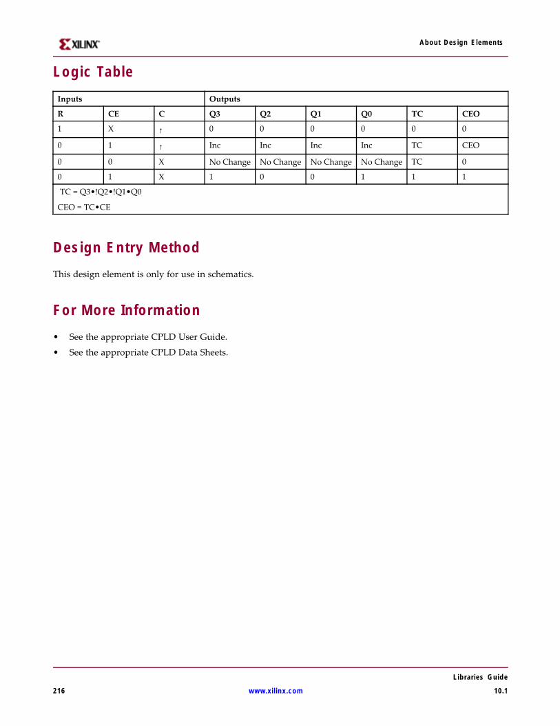
About Design Elements
Logic TableInputs Outputs
R CE C Q3 Q2 Q1 Q0 TC CEO
1 X ↑ 0 0 0 0 0 0
0 1 ↑ Inc Inc Inc Inc TC CEO
0 0 X No Change No Change No Change No Change TC 0
0 1 X 1 0 0 1 1 1
TC = Q3•!Q2•!Q1•Q0
CEO = TC•CE
Design Entry MethodThis design element is only for use in schematics.
For More Information• See the appropriate CPLD User Guide.
• See the appropriate CPLD Data Sheets.
Libraries Guide
216 www.xilinx.com 10.1

About Design Elements
CD4RLE
Macro: 4-Bit Loadable Cascadable BCD Counter with Clock Enable and Synchronous Reset
Supported Architectures
This design element is supported in the following architectures only:
• XC9500XL
• CoolRunner XPLA3
• CoolRunner-II
IntroductionCD4RLE is a 4-bit (stage), synchronous loadable, resettable, binary-coded-decimal (BCD) counter. Thesynchronous reset input (R) is the highest priority input. When R is High, all other inputs are ignored; theQ outputs, terminal count (TC), and clock enable out (CEO) go to logic level zero on the Low-to-High clocktransitions. The data on the D inputs is loaded into the counter when the load enable input (L) is High during theLow-to-High clock (C) transition. The Q outputs increment when the clock enable input (CE) is High during theLow-to-High clock transition. The counter ignores clock transitions when CE is Low. The TC output is Highwhen Q3 and Q0 are High and Q2 and Q1 are Low.
The counter recovers from any of six possible illegal states and returns to a normal count sequence within twoclock cycles for Xilinx® devices, as shown in the following state diagram:
Libraries Guide
10.1 www.xilinx.com 217
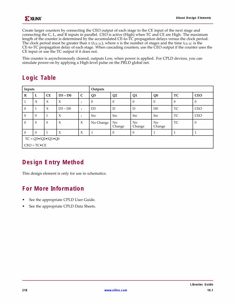
About Design Elements
Create larger counters by connecting the CEO output of each stage to the CE input of the next stage andconnecting the C, L, and R inputs in parallel. CEO is active (High) when TC and CE are High. The maximumlength of the counter is determined by the accumulated CE-to-TC propagation delays versus the clock period.The clock period must be greater than n (tCE-TC), where n is the number of stages and the time tCE-TC is theCE-to-TC propagation delay of each stage. When cascading counters, use the CEO output if the counter uses theCE input or use the TC output if it does not.
This counter is asynchronously cleared, outputs Low, when power is applied. For CPLD devices, you cansimulate power-on by applying a High-level pulse on the PRLD global net.
Logic TableInputs Outputs
R L CE D3 – D0 C Q3 Q2 Q1 Q0 TC CEO
1 X X X ↑ 0 0 0 0 0 0
0 1 X D3 – D0 ↑ D3 D D D0 TC CEO
0 0 1 X ↑ Inc Inc Inc Inc TC CEO
0 0 0 X X No Change NoChange
NoChange
NoChange
TC 0
0 0 1 X X 1 0 0 1 1 1
TC = Q3•!Q2•!Q1•Q0
CEO = TC•CE
Design Entry MethodThis design element is only for use in schematics.
For More Information• See the appropriate CPLD User Guide.
• See the appropriate CPLD Data Sheets.
Libraries Guide
218 www.xilinx.com 10.1

About Design Elements
CDD4CEMacro: 4-Bit Cascadable Dual Edge Triggered BCD Counter with Clock Enable and AsynchronousClear
Supported ArchitecturesThis design element is supported in the following architectures only:CoolRunner-II
IntroductionCDD4CE is a 4-bit (stage), asynchronous clearable, cascadable dual edge triggered Binary-coded-decimal (BCD)counter. The asynchronous clear input (CLR) is the highest priority input. When CLR is High, all other inputsare ignored; the Q outputs, terminal count (TC), and clock enable out (CEO) go to logic level zero, independentof clock transitions. The Q outputs increment when clock enable (CE) is High during the Low-to-High andHigh-to-Low clock (C) transition. The counter ignores clock transitions when CE is Low. The TC output isHigh when Q3 and Q0 are High and Q2 and Q1 are Low. The counter recovers to zero from any illegal statewithin the first clock cycle.
The counter recovers from any of six possible illegal states and returns to a normal count sequence within twoclock cycles for Xilinx® devices, as shown in the following state diagram:
Create larger counters by connecting the CEO output of each stage to the CE input of the next stage andconnecting the C and CLR inputs in parallel. CEO is active (High) when TC and CE are High. The maximumlength of the counter is determined by the accumulated CE-to-TC propagation delays versus the clock period.The clock period must be greater than n (tCE-TC), where n is the number of stages and the time tCE-TC is theCE-to-TC propagation delay of each stage. When cascading counters, use the CEO output if the counter uses theCE input or use the TC output if it does not.
This counter is asynchronously cleared, outputs Low, when power is applied. For CPLD devices, you cansimulate power-on by applying a High-level pulse on the PRLD global net.
Libraries Guide
10.1 www.xilinx.com 219

About Design Elements
Logic TableInputs Outputs
CLR CE C Q3 Q2 Q1 Q0 TC CEO
1 X X 0 0 0 0 0 0
0 1 ↑ Inc Inc Inc Inc TC CEO
0 1 ↓ Inc Inc Inc Inc TC CEO
0 0 X No Change No Change No Change No Change TC 0
0 1 X 1 0 0 1 1 1
TC = Q3•!Q2•!Q1•Q0
Design Entry MethodThis design element is only for use in schematics.
For More Information• See the appropriate CPLD User Guide.
• See the appropriate CPLD Data Sheets.
Libraries Guide
220 www.xilinx.com 10.1

About Design Elements
CDD4CLEMacro: 4-Bit Loadable Cascadable Dual Edge Triggered BCD Counter with Clock Enable andAsynchronous Clear
Supported ArchitecturesThis design element is supported in the following architectures only:CoolRunner-II
IntroductionCDD4CLE is a 4-bit (stage), synchronously loadable, asynchronously clearable, dual edge triggeredBinary-coded-decimal (BCD) counter. The asynchronous clear input (CLR) is the highest priority input. WhenCLR is High, all other inputs are ignored; the Q outputs, terminal count (TC), and clock enable out (CEO) go tologic level zero, independent of clock transitions. The data on the D inputs is loaded into the counter when theload enable input (L) is High during the Low-to-High and High-to-Low clock (C) transitions. The Q outputsincrement when clock enable input (CE) is High during the Low- to-High clock transition. The counter ignoresclock transitions when CE is Low. The TC output is High when Q3 and Q0 are High and Q2 and Q1 are Low. Thecounter recovers to zero from any illegal state within the first clock cycle.
The counter recovers from any of six possible illegal states and returns to a normal count sequence within twoclock cycles for Xilinx® devices, as shown in the following state diagram:
Create larger counters by connecting the CEO output of each stage to the CE input of the next stage andconnecting the C, L, and CLR inputs in parallel. CEO is active (High) when TC and CE are High. The maximumlength of the counter is determined by the accumulated CE-to-TC propagation delays versus the clock period.The clock period must be greater than n (tCE-TC), where n is the number of stages and the time tCE-TC is theCE-to-TC propagation delay of each stage. When cascading counters, use the CEO output if the counter uses theCE input or use the TC output if it does not.
Libraries Guide
10.1 www.xilinx.com 221

About Design Elements
This counter is asynchronously cleared, outputs Low, when power is applied. For CPLD devices, you cansimulate power-on by applying a High-level pulse on the PRLD global net.
Logic TableInputs Outputs
CLR L CE D3 – D0 C Q3 Q2 Q1 Q0 TC CEO
1 X X X X 0 0 0 0 0 0
0 1 X D3 – D0 ↑ D3 D2 D1 D0 TC CEO
0 1 X D3 – D0 ↓ D3 D2 D1 D0 TC CEO
0 0 1 X ↑ Inc Inc Inc Inc TC CEO
0 0 1 X ↓ Inc Inc Inc Inc TC CEO
0 0 0 X X NoChange
NoChange
NoChange
NoChange
TC 0
0 0 1 X X 1 0 0 1 1 1
TC = Q3•!Q2•!Q1•Q0
CEO = TC•CE
Design Entry MethodThis design element is only for use in schematics.
For More Information• See the appropriate CPLD User Guide.
• See the appropriate CPLD Data Sheets.
Libraries Guide
222 www.xilinx.com 10.1

About Design Elements
CDD4RE
Macro: 4-Bit Cascadable Dual Edge Triggered BCD Counter with Clock Enable and SynchronousReset
Supported ArchitecturesThis design element is supported in the following architectures only:CoolRunner-II
IntroductionCDD4RE is a 4-bit (stage), synchronous resettable, cascadable dual edge triggered binary-coded-decimal(BCD) counter. The synchronous reset input (R) is the highest priority input. When R is High, all other inputsare ignored; the Q outputs, terminal count (TC), and clock enable out (CEO) go to logic level zero on theLow-to-High or High-to-Low clock (C) transition. The Q outputs increment when the clock enable input (CE) isHigh during the Low-to-High and High-to-Low clock transition. The counter ignores clock transitions whenCE is Low. The TC output is High when Q3 and Q0 are High and Q2 and Q1 are Low. The counter recovers tozero from any illegal state within the first clock cycle.
The counter recovers from any of six possible illegal states and returns to a normal count sequence within twoclock cycles for Xilinx® devices, as shown in the following state diagram:
Create larger counters by connecting the CEO output of each stage to the CE input of the next stage andconnecting the C and R inputs in parallel. CEO is active (High) when TC and CE are High. The maximum lengthof the counter is determined by the accumulated CE-to-TC propagation delays versus the clock period. Theclock period must be greater than n (tCE-TC), where n is the number of stages and the time tCE-TC is the CE-to-TCpropagation delay of each stage. When cascading counters, use the CEO output if the counter uses the CEinput or use the TC output if it does not.
This counter is asynchronously cleared, outputs Low, when power is applied. For CPLD devices, you cansimulate power-on by applying a High-level pulse on the PRLD global net.
Libraries Guide
10.1 www.xilinx.com 223

About Design Elements
Logic TableInputs Outputs
R CE C Q3 Q2 Q1 Q0 TC CEO
1 X ↑ 0 0 0 0 0 0
1 X ↓ 0 0 0 0 0 0
0 1 ↑ Inc Inc Inc Inc TC CEO
0 1 ↓ Inc Inc Inc Inc TC CEO
0 0 X No Change No Change No Change No Change TC 0
0 1 X 1 0 0 1 1 1
TC = Q3•!Q2•!Q1•Q0
CEO = TC•CE
Design Entry MethodThis design element is only for use in schematics.
For More Information• See the appropriate CPLD User Guide.
• See the appropriate CPLD Data Sheets.
Libraries Guide
224 www.xilinx.com 10.1

About Design Elements
CDD4RLEMacro: 4-Bit Loadable Cascadable Dual Edge Triggered BCD Counter with Clock Enable andSynchronous Reset
Supported ArchitecturesThis design element is supported in the following architectures only:CoolRunner-II
IntroductionThis is a 4-bit (stage), synchronous loadable, resettable, dual edge triggered binary-coded-decimal (BCD) counter.The synchronous reset input (R) is the highest priority input. When R is High, all other inputs are ignored;the Q outputs, terminal count (TC), and clock enable out (CEO) go to logic level zero on the Low-to-High orHigh-to-Low clock transitions. The data on the D inputs is loaded into the counter when the load enable input(L) is High during the Low-to-High and High-to-Low clock (C) transition. The Q outputs increment when theclock enable input (CE) is High during the Low-to-High and High-to-Low clock transition. The counter ignoresclock transitions when CE is Low. The TC output is High when Q3 and Q0 are High and Q2 and Q1 are Low. Thecounter recovers to zero from any illegal state within the first clock cycle.
Larger counters are created by connecting the count enable out (CEO) output of the first stage to the CE input ofthe next stage and connecting the R, L, and C inputs in parallel. CEO is active (High) when TC and CE are High.The maximum length of the counter is determined by the accumulated CE-to-TC propagation delays versus theclock period. The clock period must be greater than n(tCE-TC), where n is the number of stages and the timetCE-TC is the CE-to-TC propagation delay of each stage. When cascading counters, use the CEO output if thecounter uses the CE input; use the TC output if it does not.
This counter is asynchronously cleared, outputs Low, when power is applied. For CPLD devices, you cansimulate power-on by applying a High-level pulse on the PRLD global net.
Design Entry MethodThis design element is only for use in schematics.
For More Information• See the appropriate CPLD User Guide.• See the appropriate CPLD Data Sheets.
Libraries Guide
10.1 www.xilinx.com 225
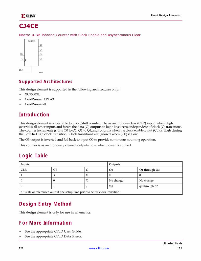
About Design Elements
CJ4CEMacro: 4-Bit Johnson Counter with Clock Enable and Asynchronous Clear
Supported ArchitecturesThis design element is supported in the following architectures only:• XC9500XL• CoolRunner XPLA3• CoolRunner-II
IntroductionThis design element is a clearable Johnson/shift counter. The asynchronous clear (CLR) input, when High,overrides all other inputs and forces the data (Q) outputs to logic level zero, independent of clock (C) transitions.The counter increments (shifts Q0 to Q1, Q1 to Q2,and so forth) when the clock enable input (CE) is High duringthe Low-to-High clock transition. Clock transitions are ignored when (CE) is Low.
The Q3 output is inverted and fed back to input Q0 to provide continuous counting operation.
This counter is asynchronously cleared, outputs Low, when power is applied.
Logic TableInputs Outputs
CLR CE C Q0 Q1 through Q3
1 X X 0 0
0 0 X No change No change
0 1 ↑ !q3 q0 through q2
q = state of referenced output one setup time prior to active clock transition
Design Entry MethodThis design element is only for use in schematics.
For More Information• See the appropriate CPLD User Guide.• See the appropriate CPLD Data Sheets.
Libraries Guide
226 www.xilinx.com 10.1

About Design Elements
CJ4REMacro: 4-Bit Johnson Counter with Clock Enable and Synchronous Reset
Supported ArchitecturesThis design element is supported in the following architectures only:• XC9500XL• CoolRunner XPLA3• CoolRunner-II
IntroductionThis design element is a resettable Johnson/shift counter. The synchronous reset (R) input, when High, overridesall other inputs and forces the data (Q) outputs to logic level zero during the Low-to-High clock (C) transition.The counter increments (shifts Q0 to Q1, Q1 to Q2, and so forth) when the clock enable input (CE) is High duringthe Low-to-High clock transition. Clock transitions are ignored when CE is Low.
The Q3 output is inverted and fed back to input Q0 to provide continuous counting operation.
This counter is asynchronously cleared, outputs Low, when power is applied.
Logic TableInputs Outputs
R CE C Q0 Q1 through Q3
1 X ↑ 0 0
0 0 X No change No change
0 1 ↑ !q3 q0 through q2
q = state of referenced output one setup time prior to active clock transition
Design Entry MethodThis design element is only for use in schematics.
For More Information• See the appropriate CPLD User Guide.• See the appropriate CPLD Data Sheets.
Libraries Guide
10.1 www.xilinx.com 227

About Design Elements
CJ5CEMacro: 5-Bit Johnson Counter with Clock Enable and Asynchronous Clear
Supported ArchitecturesThis design element is supported in the following architectures only:• XC9500XL• CoolRunner XPLA3• CoolRunner-II
IntroductionThis design element is a clearable Johnson/shift counter. The asynchronous clear (CLR) input, when High,overrides all other inputs and forces the data (Q) outputs to logic level zero, independent of clock (C) transitions.The counter increments (shifts Q0 to Q1, Q1 to Q2,and so forth) when the clock enable input (CE) is High duringthe Low-to-High clock transition. Clock transitions are ignored when (CE) is Low.
The Q4 output is inverted and fed back to input Q0 to provide continuous counting operation.
This counter is asynchronously cleared, outputs Low, when power is applied.
Logic TableInputs Outputs
CLR CE C Q0 Q1 through Q4
1 X X 0 0
0 0 X No change No change
0 1 ↑ !q4 q0 through q3
q = state of referenced output one setup time prior to active clock transition
Design Entry MethodThis design element is only for use in schematics.
For More Information• See the appropriate CPLD User Guide.
Libraries Guide
228 www.xilinx.com 10.1

About Design Elements
• See the appropriate CPLD Data Sheets.
Libraries Guide
10.1 www.xilinx.com 229

About Design Elements
CJ5REMacro: 5-Bit Johnson Counter with Clock Enable and Synchronous Reset
Supported ArchitecturesThis design element is supported in the following architectures only:• XC9500XL• CoolRunner XPLA3• CoolRunner-II
IntroductionThis design element is a resettable Johnson/shift counter. The synchronous reset (R) input, when High, overridesall other inputs and forces the data (Q) outputs to logic level zero during the Low-to-High clock (C) transition.The counter increments (shifts Q0 to Q1, Q1 to Q2, and so forth) when the clock enable input (CE) is High duringthe Low-to-High clock transition. Clock transitions are ignored when CE is Low.
The Q4 output is inverted and fed back to input Q0 to provide continuous counting operation.
This counter is asynchronously cleared, outputs Low, when power is applied.
Logic TableInputs Outputs
R CE C Q0 Q1 through Q4
1 X ↑ 0 0
0 0 X No change No change
0 1 ↑ !q4 q0 through q3
q = state of referenced output one setup time prior to active clock transition
Design Entry MethodThis design element is only for use in schematics.
For More Information• See the appropriate CPLD User Guide.
Libraries Guide
230 www.xilinx.com 10.1

About Design Elements
• See the appropriate CPLD Data Sheets.
Libraries Guide
10.1 www.xilinx.com 231
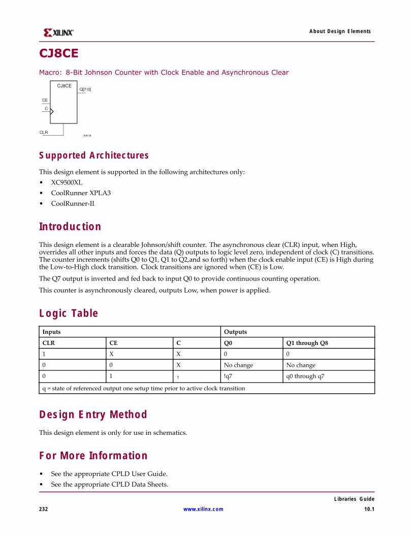
About Design Elements
CJ8CEMacro: 8-Bit Johnson Counter with Clock Enable and Asynchronous Clear
Supported ArchitecturesThis design element is supported in the following architectures only:• XC9500XL• CoolRunner XPLA3• CoolRunner-II
IntroductionThis design element is a clearable Johnson/shift counter. The asynchronous clear (CLR) input, when High,overrides all other inputs and forces the data (Q) outputs to logic level zero, independent of clock (C) transitions.The counter increments (shifts Q0 to Q1, Q1 to Q2,and so forth) when the clock enable input (CE) is High duringthe Low-to-High clock transition. Clock transitions are ignored when (CE) is Low.
The Q7 output is inverted and fed back to input Q0 to provide continuous counting operation.
This counter is asynchronously cleared, outputs Low, when power is applied.
Logic TableInputs Outputs
CLR CE C Q0 Q1 through Q8
1 X X 0 0
0 0 X No change No change
0 1 ↑ !q7 q0 through q7
q = state of referenced output one setup time prior to active clock transition
Design Entry MethodThis design element is only for use in schematics.
For More Information• See the appropriate CPLD User Guide.• See the appropriate CPLD Data Sheets.
Libraries Guide
232 www.xilinx.com 10.1

About Design Elements
CJ8REMacro: 8-Bit Johnson Counter with Clock Enable and Synchronous Reset
Supported ArchitecturesThis design element is supported in the following architectures only:• XC9500XL• CoolRunner XPLA3• CoolRunner-II
IntroductionThis design element is a resettable Johnson/shift counter. The synchronous reset (R) input, when High, overridesall other inputs and forces the data (Q) outputs to logic level zero during the Low-to-High clock (C) transition.The counter increments (shifts Q0 to Q1, Q1 to Q2, and so forth) when the clock enable input (CE) is High duringthe Low-to-High clock transition. Clock transitions are ignored when CE is Low.
The Q7 output is inverted and fed back to input Q0 to provide continuous counting operation.
This counter is asynchronously cleared, outputs Low, when power is applied.
Logic TableInputs Outputs
R CE C Q0 Q1 through Q7
1 X ↑ 0 0
0 0 X No change No change
0 1 ↑ !q7 q0 through q6
q = state of referenced output one setup time prior to active clock transition
Design Entry MethodThis design element is only for use in schematics.
For More Information• See the appropriate CPLD User Guide.• See the appropriate CPLD Data Sheets.
Libraries Guide
10.1 www.xilinx.com 233

About Design Elements
CJD4CEMacro: 4-Bit Dual Edge Triggered Johnson Counter with Clock Enable and Asynchronous Clear
Supported ArchitecturesThis design element is supported in the following architectures only:CoolRunner-II
IntroductionThis element is a dual edge triggered clearable Johnson/shift counter. The asynchronous clear (CLR) input, whenHigh, overrides all other inputs and causes the data (Q) outputs to go to logic level zero independent of clock (C)transitions. The counter increments (shifts Q0 to Q1, Q1 to Q2,etc.) when the clock enable input (CE) is Highduring the Low-to-High and High-to-Low clock transition. Clock transitions are ignored when CE is Low.
The Q3 output is inverted and fed back to input Q0 to provide continuous counting operation.
This counter is asynchronously cleared, outputs Low, when power is applied. For CPLD devices, you cansimulate power-on by applying a High-level pulse on the PRLD global net.
Logic TableInputs Outputs
CLR CE C Q0 Q1 through Q3
1 X X 0 0
0 0 X No Change No Change
0 1 ↑ !q3 q0 through q2
0 1 ↓ !q3 q0 through q2
q = state of referenced output one setup time prior to active clock transition
Design Entry MethodThis design element is only for use in schematics.
For More Information• See the appropriate CPLD User Guide.• See the appropriate CPLD Data Sheets.
Libraries Guide
234 www.xilinx.com 10.1

About Design Elements
CJD4RE
Macro: 4-Bit Dual Edge Triggered Johnson Counter with Clock Enable and Synchronous Reset
Supported Architectures
This design element is supported in the following architectures only:CoolRunner-II
IntroductionThis design element is a resettable dual edge triggered Johnson/shift counter. The synchronous reset (R) input,when High, overrides all other inputs and causes the data (Q) outputs to go to logic level zero during theLow-to-High and High-to-Low clock (C) transitions. The counter increments (shifts Q0 to Q1, Q1 to Q2, etc.)when the clock enable input (CE) is High during the Low-to-High and High-to-Low clock transition. Clocktransitions are ignored when CE is Low.
The Q3 output is inverted and fed back to input Q0 to provide continuous counting operation.
This counter is asynchronously cleared, outputs Low, when power is applied. For CPLD devices, you cansimulate power-on by applying a High-level pulse on the PRLD global net.
Logic TableInputs Outputs
R CE C Q0 Q1 – Q3
1 X ↑ 0 0
1 X ↓ 0 0
0 0 X No Change No Change
0 1 ↑ !q3 q0 – q2
0 1 ↓ !q3 q0 – q2
q = state of referenced output one setup time prior to active clock transition
Design Entry MethodThis design element is only for use in schematics.
Libraries Guide
10.1 www.xilinx.com 235

About Design Elements
For More Information• See the appropriate CPLD User Guide.
• See the appropriate CPLD Data Sheets.
Libraries Guide
236 www.xilinx.com 10.1

About Design Elements
CJD5CEMacro: 5-Bit Dual Edge Triggered Johnson Counter with Clock Enable and Asynchronous Clear
Supported ArchitecturesThis design element is supported in the following architectures only:CoolRunner-II
IntroductionThis element is a dual edge triggered clearable Johnson/shift counter. The asynchronous clear (CLR) input, whenHigh, overrides all other inputs and causes the data (Q) outputs to go to logic level zero independent of clock (C)transitions. The counter increments (shifts Q0 to Q1, Q1 to Q2,etc.) when the clock enable input (CE) is Highduring the Low-to-High and High-to-Low clock transition. Clock transitions are ignored when CE is Low.
The Q4 output is inverted and fed back to input Q0 to provide continuous counting operation.
This counter is asynchronously cleared, outputs Low, when power is applied. For CPLD devices, you cansimulate power-on by applying a High-level pulse on the PRLD global net.
Logic TableInputs Outputs
CLR CE C Q0 Q1 through Q4
1 X X 0 0
0 0 X No Change No Change
0 1 ↑ !q4 q0 through q3
0 1 ↓ !q4 q0 through q3
q = state of referenced output one setup time prior to active clock transition
Design Entry MethodThis design element is only for use in schematics.
For More Information• See the appropriate CPLD User Guide.
Libraries Guide
10.1 www.xilinx.com 237

About Design Elements
• See the appropriate CPLD Data Sheets.
Libraries Guide
238 www.xilinx.com 10.1

About Design Elements
CJD5RE
Macro: 5-Bit Dual Edge Triggered Johnson Counter with Clock Enable and Synchronous Reset
Supported ArchitecturesThis design element is supported in the following architectures only:CoolRunner-II
IntroductionThis design element is a resettable dual edge triggered Johnson/shift counter. The synchronous reset (R) input,when High, overrides all other inputs and causes the data (Q) outputs to go to logic level zero during theLow-to-High and High-to-Low clock (C) transitions. The counter increments (shifts Q0 to Q1, Q1 to Q2, etc.)when the clock enable input (CE) is High during the Low-to-High and High-to-Low clock transition. Clocktransitions are ignored when CE is Low.
The Q4 output is inverted and fed back to input Q0 to provide continuous counting operation.
This counter is asynchronously cleared, outputs Low, when power is applied. For CPLD devices, you cansimulate power-on by applying a High-level pulse on the PRLD global net.
Logic TableInputs Outputs
R CE C Q0 Q1 – Q4
1 X ↑ 0 0
1 X ↓ 0 0
0 0 X No Change No Change
0 1 ↑ !q4 q0 – q3
0 1 ↓ !q4 q0 – q3
q = state of referenced output one setup time prior to active clock transition
Design Entry MethodThis design element is only for use in schematics.
Libraries Guide
10.1 www.xilinx.com 239

About Design Elements
For More Information• See the appropriate CPLD User Guide.
• See the appropriate CPLD Data Sheets.
Libraries Guide
240 www.xilinx.com 10.1

About Design Elements
CJD8CEMacro: 8-Bit Dual Edge Triggered Johnson Counter with Clock Enable and Asynchronous Clear
Supported ArchitecturesThis design element is supported in the following architectures only:CoolRunner-II
IntroductionThis element is a dual edge triggered clearable Johnson/shift counter. The asynchronous clear (CLR) input, whenHigh, overrides all other inputs and causes the data (Q) outputs to go to logic level zero independent of clock (C)transitions. The counter increments (shifts Q0 to Q1, Q1 to Q2,etc.) when the clock enable input (CE) is Highduring the Low-to-High and High-to-Low clock transition. Clock transitions are ignored when CE is Low.
The Q7 output is inverted and fed back to input Q0 to provide continuous counting operation.
This counter is asynchronously cleared, outputs Low, when power is applied. For CPLD devices, you cansimulate power-on by applying a High-level pulse on the PRLD global net.
Logic TableInputs Outputs
CLR CE C Q0 Q1 through Q7
1 X X 0 0
0 0 X No Change No Change
0 1 ↑ !q7 q0 through q6
0 1 ↓ !q7 q0 through q6
q = state of referenced output one setup time prior to active clock transition
Design Entry MethodThis design element is only for use in schematics.
For More Information• See the appropriate CPLD User Guide.• See the appropriate CPLD Data Sheets.
Libraries Guide
10.1 www.xilinx.com 241

About Design Elements
CJD8REMacro: 8-Bit Dual Edge Triggered Johnson Counter with Clock Enable and Synchronous Reset
Supported ArchitecturesThis design element is supported in the following architectures only:CoolRunner-II
IntroductionThis design element is a resettable dual edge triggered Johnson/shift counter. The synchronous reset (R) input,when High, overrides all other inputs and causes the data (Q) outputs to go to logic level zero during theLow-to-High and High-to-Low clock (C) transitions. The counter increments (shifts Q0 to Q1, Q1 to Q2, etc.)when the clock enable input (CE) is High during the Low-to-High and High-to-Low clock transition. Clocktransitions are ignored when CE is Low.
The Q7 output is inverted and fed back to input Q0 to provide continuous counting operation.
This counter is asynchronously cleared, outputs Low, when power is applied. For CPLD devices, you cansimulate power-on by applying a High-level pulse on the PRLD global net.
Logic TableInputs Outputs
R CE C Q0 Q1 – Q7
1 X ↑ 0 0
1 X ↓ 0 0
0 0 X No Change No Change
0 1 ↑ !q7 q0 – q6
0 1 ↓ !q7 q0 – q6
q = state of referenced output one setup time prior to active clock transition
Design Entry MethodThis design element is only for use in schematics.
For More Information• See the appropriate CPLD User Guide.
Libraries Guide
242 www.xilinx.com 10.1

About Design Elements
• See the appropriate CPLD Data Sheets.
Libraries Guide
10.1 www.xilinx.com 243
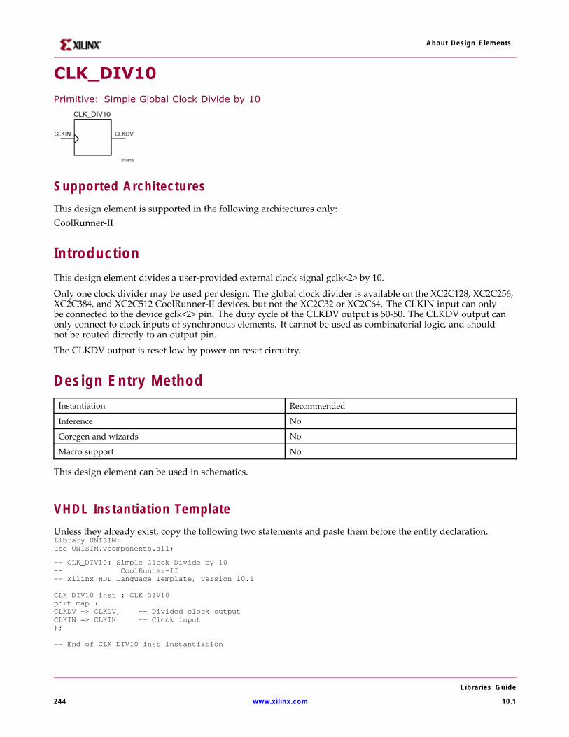
About Design Elements
CLK_DIV10Primitive: Simple Global Clock Divide by 10
Supported ArchitecturesThis design element is supported in the following architectures only:CoolRunner-II
IntroductionThis design element divides a user-provided external clock signal gclk<2> by 10.
Only one clock divider may be used per design. The global clock divider is available on the XC2C128, XC2C256,XC2C384, and XC2C512 CoolRunner-II devices, but not the XC2C32 or XC2C64. The CLKIN input can onlybe connected to the device gclk<2> pin. The duty cycle of the CLKDV output is 50-50. The CLKDV output canonly connect to clock inputs of synchronous elements. It cannot be used as combinatorial logic, and shouldnot be routed directly to an output pin.
The CLKDV output is reset low by power-on reset circuitry.
Design Entry MethodInstantiation Recommended
Inference No
Coregen and wizards No
Macro support No
This design element can be used in schematics.
VHDL Instantiation TemplateUnless they already exist, copy the following two statements and paste them before the entity declaration.Library UNISIM;use UNISIM.vcomponents.all;
-- CLK_DIV10: Simple Clock Divide by 10-- CoolRunner-II-- Xilinx HDL Language Template, version 10.1
CLK_DIV10_inst : CLK_DIV10port map (CLKDV => CLKDV, -- Divided clock outputCLKIN => CLKIN -- Clock input);
-- End of CLK_DIV10_inst instantiation
Libraries Guide
244 www.xilinx.com 10.1

About Design Elements
Verilog Instantiation Template// CLK_DIV10: Simple Clock Divide by 10// CoolRunner-II// Xilinx HDL Language Template, version 10.1
CLK_DIV10 CLK_DIV10_inst (.CLKDV(CLKDV), // Divided clock output.CLKIN(CLKIN) // Clock input);
// End of CLK_DIV10_inst instantiation
For More Information• See the appropriate CPLD User Guide.
• See the appropriate CPLD Data Sheets.
Libraries Guide
10.1 www.xilinx.com 245

About Design Elements
CLK_DIV10RPrimitive: Global Clock Divide by 10 with Synchronous Reset
Supported ArchitecturesThis design element is supported in the following architectures only:CoolRunner-II
IntroductionThis design element divides a user-provided external clock signal gclk<2> by 10.
Only one clock divider may be used per design. The global clock divider is available on the XC2C128, XC2C256,XC2C384, and XC2C512 CoolRunner-II devices, but not the XC2C32 or XC2C64. The CLKIN and CDRST inputscan only be connected to the device gclk<2> and CDRST pins. The duty cycle of the CLKDV output is 50-50. TheCLKDV output can only connect to clock inputs of synchronous elements. It cannot be used as combinatoriallogic, and should not be routed directly to an output pin.
The CDRST input is an active High synchronous reset. If CDRST is input High when the CLKDV output is High,the CLKDV output remains High to complete the last clock pulse, and then goes Low.
The CLKDV output is reset low by power-on reset circuitry.
Design Entry MethodInstantiation Recommended
Inference No
Coregen and wizards No
Macro support No
This design element can be used in schematics.
VHDL Instantiation TemplateUnless they already exist, copy the following two statements and paste them before the entity declaration.Library UNISIM;use UNISIM.vcomponents.all;
-- CLK_DIV10R: Clock Divide by 10 with Synchronous Reset-- CoolRunner-II-- Xilinx HDL Language Template, version 10.1
CLK_DIV10R_inst : CLK_DIV10Rport map (CLKDV => CLKDV, -- Divided clock outputCDRST => CDRST, -- Synchronous reset inputCLKIN => CLKIN -- Clock input);
Libraries Guide
246 www.xilinx.com 10.1

About Design Elements
-- End of CLK_DIV10R_inst instantiation
Verilog Instantiation Template// CLK_DIV10R: Clock Divide by 10 with Synchronous Reset// CoolRunner-II// Xilinx HDL Language Template, version 10.1
CLK_DIV10R CLK_DIV10R_inst (.CLKDV(CLKDV), // Divided clock output.CDRST(CDRST), // Synchronous reset input.CLKIN(CLKIN) // Clock input);
// End of CLK_DIV10R_inst instantiation
For More Information• See the appropriate CPLD User Guide.
• See the appropriate CPLD Data Sheets.
Libraries Guide
10.1 www.xilinx.com 247

About Design Elements
CLK_DIV10RSDPrimitive: Global Clock Divide by 10 with Synchronous Reset and Start Delay
Supported ArchitecturesThis design element is supported in the following architectures only:CoolRunner-II
IntroductionThis design element divides a user-provided external clock signal gclk<2> by 10.
Only one clock divider may be used per design. The global clock divider is available on the XC2C128, XC2C256,XC2C384, and XC2C512 CoolRunner-II devices, but not the XC2C32 or XC2C64. The CLKIN and CDRST inputscan only be connected to the device gclk<2> and CDRST pins. The duty cycle of the CLKDV output is 50-50. TheCLKDV output can only connect to clock inputs of synchronous elements. It cannot be used as combinatoriallogic, and should not be routed directly to an output pin.
The CDRST input is an active High synchronous reset. If CDRST is input High when the CLKDV output is High,the CLKDV output remains High to complete the last clock pulse, and then goes Low.
The start delay function delays the start of the CLKDV output by (n + 1) clocks, where n is the divisor forthe clock divider.
The CLKDV output is reset low by power-on reset circuitry.
Design Entry MethodInstantiation Recommended
Inference No
Coregen and wizards No
Macro support No
This design element can be used in schematics.
VHDL Instantiation TemplateUnless they already exist, copy the following two statements and paste them before the entity declaration.Library UNISIM;use UNISIM.vcomponents.all;
-- CLK_DIV10RSD: Clock Divide by 10 with Synchronous Reset and Start-- Delay-- CoolRunner-II-- Xilinx HDL Language Template, version 10.1
CLK_DIV10RSD_inst : CLK_DIV10RSD-- Edit the following generic to specify the number of clock cycles-- to delay before starting.
Libraries Guide
248 www.xilinx.com 10.1
About Design Elements
generic map (DIVIDER_DELAY => 1)port map (CLKDV => CLKDV, -- Divided clock outputCDRST => CDRST, -- Synchronous reset inputCLKIN => CLKIN -- Clock input);
-- End of CLK_DIV10RSD_inst instantiation
Verilog Instantiation Template// CLK_DIV12RSD: Clock Divide by 12 with Synchronous Reset and Start// Delay// CoolRunner-II// Xilinx HDL Language Template, version 10.1
CLK_DIV12RSD CLK_DIV12RSD_inst (.CLKDV(CLKDV), // Divided clock output.CDRST(CDRST), // Synchronous reset input.CLKIN(CLKIN) // Clock input);
// Edit the following defparam to specify the number of clock// cycles to delay before starting. If the instance name to// the clock divider is changed, that change needs to be// reflected in the defparam statements.
defparam CLK_DIV12RSD_inst.DIVIDER_DELAY = 1;
// End of CLK_DIV12RSD_inst instantiation
For More Information• See the appropriate CPLD User Guide.
• See the appropriate CPLD Data Sheets.
Libraries Guide
10.1 www.xilinx.com 249

About Design Elements
CLK_DIV10SDPrimitive: Global Clock Divide by 10 with Start Delay
Supported ArchitecturesThis design element is supported in the following architectures only:CoolRunner-II
IntroductionThis design element divides a user-provided external clock signal gclk<2> by 10.
Only one clock divider may be used per design. The global clock divider is available on the XC2C128, XC2C256,XC2C384, and XC2C512 CoolRunner-II devices, but not the XC2C32 or XC2C64. The CLKIN input can onlybe connected to the device gclk<2> pin. The duty cycle of the CLKDV output is 50-50. The CLKDV output canonly connect to clock inputs of synchronous elements. It cannot be used as combinatorial logic, and shouldnot be routed directly to an output pin.
The start delay function delays the start of the CLKDV output by (n + 1) clocks, where n is the divisor forthe clock divider.
The CLKDV output is reset low by power-on reset circuitry.
Design Entry MethodInstantiation Recommended
Inference No
Coregen and wizards No
Macro support No
This design element can be used in schematics.
VHDL Instantiation TemplateUnless they already exist, copy the following two statements and paste them before the entity declaration.Library UNISIM;use UNISIM.vcomponents.all;
-- CLK_DIV10SD: Clock Divide by 10 with Start Delay-- CoolRunner-II-- Xilinx HDL Language Template, version 10.1
CLK_DIV10SD_inst : CLK_DIV10SD-- Edit the following generic to specify the number of clock cycles-- to delay before starting.generic map (DIVIDER_DELAY => 1)port map (CLKDV => CLKDV, -- Divided clock output
Libraries Guide
250 www.xilinx.com 10.1

About Design Elements
CLKIN => CLKIN -- Clock input);
-- End of CLK_DIV10SD_inst instantiation
Verilog Instantiation Template// CLK_DIV10SD: Clock Divide by 10 with Start Delay// CoolRunner-II// Xilinx HDL Language Template, version 10.1
CLK_DIV10SD CLK_DIV10SD_inst (.CLKDV(CLKDV), // Divided clock output.CDRST(CDRST), // Synchronous reset input.CLKIN(CLKIN) // Clock input);
// Edit the following defparam to specify the number of clock// cycles to delay before starting. If the instance name to// the clock divider is changed, that change needs to be// reflected in the defparam statements.
defparam CLK_DIV10SD_inst.DIVIDER_DELAY = 1;
// End of CLK_DIV10SD_inst instantiation
For More Information• See the appropriate CPLD User Guide.
• See the appropriate CPLD Data Sheets.
Libraries Guide
10.1 www.xilinx.com 251

About Design Elements
CLK_DIV12Primitive: Simple Global Clock Divide by 12
Supported ArchitecturesThis design element is supported in the following architectures only:CoolRunner-II
IntroductionThis design element divides a user-provided external clock signal gclk<2> by 12.
Only one clock divider may be used per design. The global clock divider is available on the XC2C128, XC2C256,XC2C384, and XC2C512 CoolRunner-II devices, but not the XC2C32 or XC2C64. The CLKIN input can onlybe connected to the device gclk<2> pin. The duty cycle of the CLKDV output is 50-50. The CLKDV output canonly connect to clock inputs of synchronous elements. It cannot be used as combinatorial logic, and shouldnot be routed directly to an output pin.
The CLKDV output is reset low by power-on reset circuitry.
Design Entry MethodInstantiation Recommended
Inference No
Coregen and wizards No
Macro support No
This design element can be used in schematics.
VHDL Instantiation TemplateUnless they already exist, copy the following two statements and paste them before the entity declaration.Library UNISIM;use UNISIM.vcomponents.all;
-- CLK_DIV12: Simple Clock Divide by 12-- CoolRunner-II-- Xilinx HDL Language Template, version 10.1
CLK_DIV12_inst : CLK_DIV12port map (CLKDV => CLKDV, -- Divided clock outputCLKIN => CLKIN -- Clock input);
-- End of CLK_DIV12_inst instantiation
Libraries Guide
252 www.xilinx.com 10.1

About Design Elements
Verilog Instantiation Template// CLK_DIV12: Simple Clock Divide by 12// CoolRunner-II// Xilinx HDL Language Template, version 10.1
CLK_DIV12 CLK_DIV12_inst (.CLKDV(CLKDV), // Divided clock output.CLKIN(CLKIN) // Clock input);
// End of CLK_DIV12_inst instantiation
For More Information• See the appropriate CPLD User Guide.
• See the appropriate CPLD Data Sheets.
Libraries Guide
10.1 www.xilinx.com 253

About Design Elements
CLK_DIV12RPrimitive: Global Clock Divide by 12 with Synchronous Reset
Supported ArchitecturesThis design element is supported in the following architectures only:CoolRunner-II
IntroductionThis design element divides a user-provided external clock signal gclk<2> by 12.
Only one clock divider may be used per design. The global clock divider is available on the XC2C128, XC2C256,XC2C384, and XC2C512 CoolRunner-II devices, but not the XC2C32 or XC2C64. The CLKIN and CDRST inputscan only be connected to the device gclk<2> and CDRST pins. The duty cycle of the CLKDV output is 50-50. TheCLKDV output can only connect to clock inputs of synchronous elements. It cannot be used as combinatoriallogic, and should not be routed directly to an output pin.
The CDRST input is an active High synchronous reset. If CDRST is input High when the CLKDV output is High,the CLKDV output remains High to complete the last clock pulse, and then goes Low.
The CLKDV output is reset low by power-on reset circuitry.
Design Entry MethodInstantiation Recommended
Inference No
Coregen and wizards No
Macro support No
This design element can be used in schematics.
VHDL Instantiation TemplateUnless they already exist, copy the following two statements and paste them before the entity declaration.Library UNISIM;use UNISIM.vcomponents.all;
-- CLK_DIV12R: Clock Divide by 12 with Synchronous Reset-- CoolRunner-II-- Xilinx HDL Language Template, version 10.1
CLK_DIV12R_inst : CLK_DIV12Rport map (CLKDV => CLKDV, -- Divided clock outputCDRST => CDRST, -- Synchronous reset inputCLKIN => CLKIN -- Clock input);
Libraries Guide
254 www.xilinx.com 10.1

About Design Elements
-- End of CLK_DIV12R_inst instantiation
Verilog Instantiation Template// CLK_DIV12R: Clock Divide by 12 with Synchronous Reset// CoolRunner-II// Xilinx HDL Language Template, version 10.1
CLK_DIV12R CLK_DIV12R_inst (.CLKDV(CLKDV), // Divided clock output.CDRST(CDRST), // Synchronous reset input.CLKIN(CLKIN) // Clock input);
// End of CLK_DIV12R_inst instantiation
For More Information• See the appropriate CPLD User Guide.
• See the appropriate CPLD Data Sheets.
Libraries Guide
10.1 www.xilinx.com 255

About Design Elements
CLK_DIV12RSDPrimitive: Global Clock Divide by 12 with Synchronous Reset and Start Delay
Supported ArchitecturesThis design element is supported in the following architectures only:CoolRunner-II
IntroductionThis design element divides a user-provided external clock signal gclk<2> by 12.
Only one clock divider may be used per design. The global clock divider is available on the XC2C128, XC2C256,XC2C384, and XC2C512 CoolRunner-II devices, but not the XC2C32 or XC2C64. The CLKIN and CDRST inputscan only be connected to the device gclk<2> and CDRST pins. The duty cycle of the CLKDV output is 50-50. TheCLKDV output can only connect to clock inputs of synchronous elements. It cannot be used as combinatoriallogic, and should not be routed directly to an output pin.
The CDRST input is an active High synchronous reset. If CDRST is input High when the CLKDV output is High,the CLKDV output remains High to complete the last clock pulse, and then goes Low.
The start delay function delays the start of the CLKDV output by (n + 1) clocks, where n is the divisor forthe clock divider.
The CLKDV output is reset low by power-on reset circuitry.
Design Entry MethodInstantiation Recommended
Inference No
Coregen and wizards No
Macro support No
This design element can be used in schematics.
VHDL Instantiation TemplateUnless they already exist, copy the following two statements and paste them before the entity declaration.Library UNISIM;use UNISIM.vcomponents.all;
-- CLK_DIV12RSD: Clock Divide by 12 with Synchronous Reset and Start-- Delay-- CoolRunner-II-- Xilinx HDL Language Template, version 10.1
CLK_DIV12RSD_inst : CLK_DIV12RSD-- Edit the following generic to specify the number of clock cycles-- to delay before starting.
Libraries Guide
256 www.xilinx.com 10.1

About Design Elements
generic map (DIVIDER_DELAY => 1)port map (CLKDV => CLKDV, -- Divided clock outputCDRST => CDRST, -- Synchronous reset inputCLKIN => CLKIN -- Clock input);
-- End of CLK_DIV12RSD_inst instantiation
Verilog Instantiation Template// CLK_DIV12RSD: Clock Divide by 12 with Synchronous Reset and Start// Delay// CoolRunner-II// Xilinx HDL Language Template, version 10.1
CLK_DIV12RSD CLK_DIV12RSD_inst (.CLKDV(CLKDV), // Divided clock output.CDRST(CDRST), // Synchronous reset input.CLKIN(CLKIN) // Clock input);
// Edit the following defparam to specify the number of clock// cycles to delay before starting. If the instance name to// the clock divider is changed, that change needs to be// reflected in the defparam statements.
defparam CLK_DIV12RSD_inst.DIVIDER_DELAY = 1;
// End of CLK_DIV12RSD_inst instantiation
For More Information• See the appropriate CPLD User Guide.
• See the appropriate CPLD Data Sheets.
Libraries Guide
10.1 www.xilinx.com 257
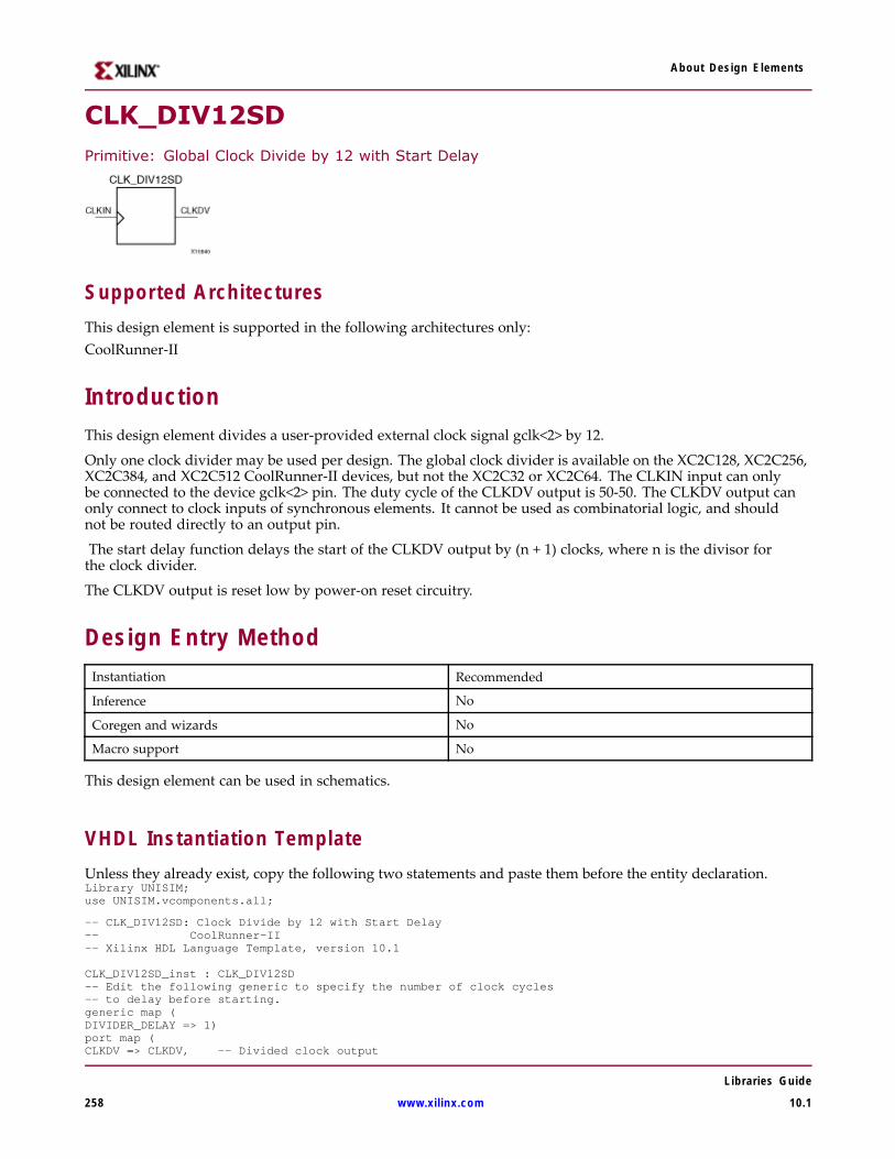
About Design Elements
CLK_DIV12SDPrimitive: Global Clock Divide by 12 with Start Delay
Supported ArchitecturesThis design element is supported in the following architectures only:CoolRunner-II
IntroductionThis design element divides a user-provided external clock signal gclk<2> by 12.
Only one clock divider may be used per design. The global clock divider is available on the XC2C128, XC2C256,XC2C384, and XC2C512 CoolRunner-II devices, but not the XC2C32 or XC2C64. The CLKIN input can onlybe connected to the device gclk<2> pin. The duty cycle of the CLKDV output is 50-50. The CLKDV output canonly connect to clock inputs of synchronous elements. It cannot be used as combinatorial logic, and shouldnot be routed directly to an output pin.
The start delay function delays the start of the CLKDV output by (n + 1) clocks, where n is the divisor forthe clock divider.
The CLKDV output is reset low by power-on reset circuitry.
Design Entry MethodInstantiation Recommended
Inference No
Coregen and wizards No
Macro support No
This design element can be used in schematics.
VHDL Instantiation TemplateUnless they already exist, copy the following two statements and paste them before the entity declaration.Library UNISIM;use UNISIM.vcomponents.all;
-- CLK_DIV12SD: Clock Divide by 12 with Start Delay-- CoolRunner-II-- Xilinx HDL Language Template, version 10.1
CLK_DIV12SD_inst : CLK_DIV12SD-- Edit the following generic to specify the number of clock cycles-- to delay before starting.generic map (DIVIDER_DELAY => 1)port map (CLKDV => CLKDV, -- Divided clock output
Libraries Guide
258 www.xilinx.com 10.1

About Design Elements
CLKIN => CLKIN -- Clock input);
-- End of CLK_DIV12SD_inst instantiation
Verilog Instantiation Template// CLK_DIV12SD: Clock Divide by 12 with Start Delay// CoolRunner-II// Xilinx HDL Language Template, version 10.1
CLK_DIV12SD CLK_DIV12SD_inst (.CLKDV(CLKDV), // Divided clock output.CDRST(CDRST), // Synchronous reset input.CLKIN(CLKIN) // Clock input);
// Edit the following defparam to specify the number of clock// cycles to delay before starting. If the instance name to// the clock divider is changed, that change needs to be// reflected in the defparam statements.
defparam CLK_DIV12SD_inst.DIVIDER_DELAY = 1;
// End of CLK_DIV12SD_inst instantiation
For More Information• See the appropriate CPLD User Guide.
• See the appropriate CPLD Data Sheets.
Libraries Guide
10.1 www.xilinx.com 259

About Design Elements
CLK_DIV14Primitive: Simple Global Clock Divide by 14
Supported ArchitecturesThis design element is supported in the following architectures only:CoolRunner-II
IntroductionThis design element divides a user-provided external clock signal gclk<2> by 14.
Only one clock divider may be used per design. The global clock divider is available on the XC2C128, XC2C256,XC2C384, and XC2C512 CoolRunner-II devices, but not the XC2C32 or XC2C64. The CLKIN input can onlybe connected to the device gclk<2> pin. The duty cycle of the CLKDV output is 50-50. The CLKDV output canonly connect to clock inputs of synchronous elements. It cannot be used as combinatorial logic, and shouldnot be routed directly to an output pin.
The CLKDV output is reset low by power-on reset circuitry.
Design Entry MethodInstantiation Recommended
Inference No
Coregen and wizards No
Macro support No
This design element can be used in schematics.
VHDL Instantiation TemplateUnless they already exist, copy the following two statements and paste them before the entity declaration.Library UNISIM;use UNISIM.vcomponents.all;
-- CLK_DIV14: Simple Clock Divide by 14-- CoolRunner-II-- Xilinx HDL Language Template, version 10.1
CLK_DIV14_inst : CLK_DIV14port map (CLKDV => CLKDV, -- Divided clock outputCLKIN => CLKIN -- Clock input);
-- End of CLK_DIV14_inst instantiation
Libraries Guide
260 www.xilinx.com 10.1

About Design Elements
Verilog Instantiation Template// CLK_DIV14: Simple Clock Divide by 14// CoolRunner-II// Xilinx HDL Language Template, version 10.1
CLK_DIV14 CLK_DIV14_inst (.CLKDV(CLKDV), // Divided clock output.CLKIN(CLKIN) // Clock input);
// End of CLK_DIV14_inst instantiation
For More Information• See the appropriate CPLD User Guide.
• See the appropriate CPLD Data Sheets.
Libraries Guide
10.1 www.xilinx.com 261
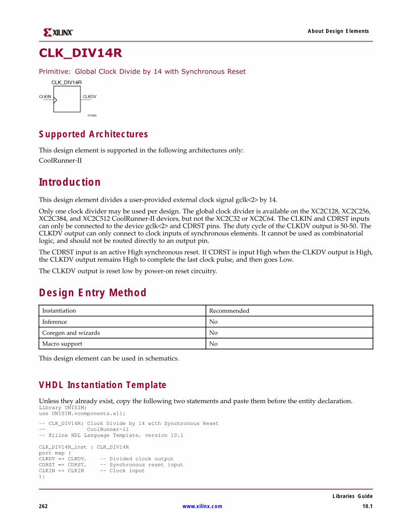
About Design Elements
CLK_DIV14RPrimitive: Global Clock Divide by 14 with Synchronous Reset
Supported ArchitecturesThis design element is supported in the following architectures only:CoolRunner-II
IntroductionThis design element divides a user-provided external clock signal gclk<2> by 14.
Only one clock divider may be used per design. The global clock divider is available on the XC2C128, XC2C256,XC2C384, and XC2C512 CoolRunner-II devices, but not the XC2C32 or XC2C64. The CLKIN and CDRST inputscan only be connected to the device gclk<2> and CDRST pins. The duty cycle of the CLKDV output is 50-50. TheCLKDV output can only connect to clock inputs of synchronous elements. It cannot be used as combinatoriallogic, and should not be routed directly to an output pin.
The CDRST input is an active High synchronous reset. If CDRST is input High when the CLKDV output is High,the CLKDV output remains High to complete the last clock pulse, and then goes Low.
The CLKDV output is reset low by power-on reset circuitry.
Design Entry MethodInstantiation Recommended
Inference No
Coregen and wizards No
Macro support No
This design element can be used in schematics.
VHDL Instantiation TemplateUnless they already exist, copy the following two statements and paste them before the entity declaration.Library UNISIM;use UNISIM.vcomponents.all;
-- CLK_DIV14R: Clock Divide by 14 with Synchronous Reset-- CoolRunner-II-- Xilinx HDL Language Template, version 10.1
CLK_DIV14R_inst : CLK_DIV14Rport map (CLKDV => CLKDV, -- Divided clock outputCDRST => CDRST, -- Synchronous reset inputCLKIN => CLKIN -- Clock input);
Libraries Guide
262 www.xilinx.com 10.1

About Design Elements
-- End of CLK_DIV14R_inst instantiation
Verilog Instantiation Template// CLK_DIV14R: Clock Divide by 14 with Synchronous Reset// CoolRunner-II// Xilinx HDL Language Template, version 10.1
CLK_DIV14R CLK_DIV14R_inst (.CLKDV(CLKDV), // Divided clock output.CDRST(CDRST), // Synchronous reset input.CLKIN(CLKIN) // Clock input);
// End of CLK_DIV14R_inst instantiation
For More Information• See the appropriate CPLD User Guide.
• See the appropriate CPLD Data Sheets.
Libraries Guide
10.1 www.xilinx.com 263
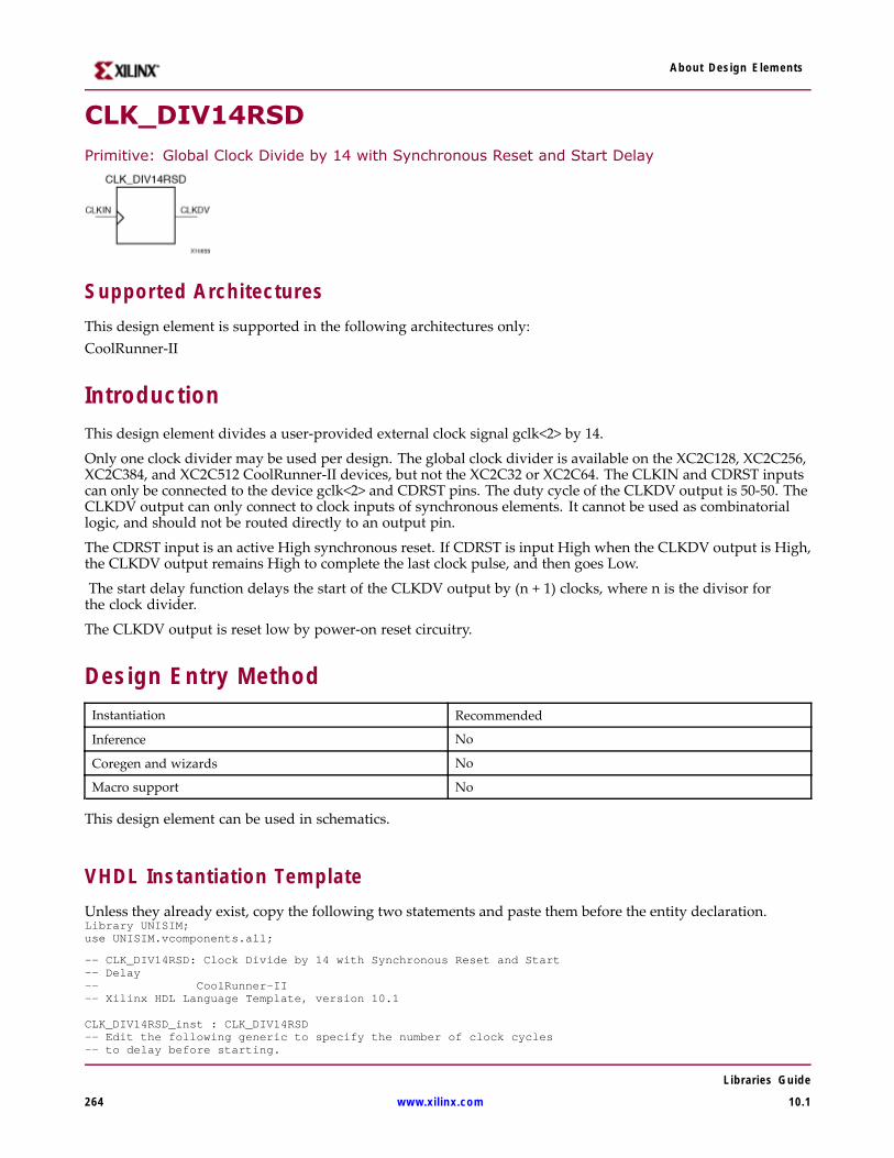
About Design Elements
CLK_DIV14RSDPrimitive: Global Clock Divide by 14 with Synchronous Reset and Start Delay
Supported ArchitecturesThis design element is supported in the following architectures only:CoolRunner-II
IntroductionThis design element divides a user-provided external clock signal gclk<2> by 14.
Only one clock divider may be used per design. The global clock divider is available on the XC2C128, XC2C256,XC2C384, and XC2C512 CoolRunner-II devices, but not the XC2C32 or XC2C64. The CLKIN and CDRST inputscan only be connected to the device gclk<2> and CDRST pins. The duty cycle of the CLKDV output is 50-50. TheCLKDV output can only connect to clock inputs of synchronous elements. It cannot be used as combinatoriallogic, and should not be routed directly to an output pin.
The CDRST input is an active High synchronous reset. If CDRST is input High when the CLKDV output is High,the CLKDV output remains High to complete the last clock pulse, and then goes Low.
The start delay function delays the start of the CLKDV output by (n + 1) clocks, where n is the divisor forthe clock divider.
The CLKDV output is reset low by power-on reset circuitry.
Design Entry MethodInstantiation Recommended
Inference No
Coregen and wizards No
Macro support No
This design element can be used in schematics.
VHDL Instantiation TemplateUnless they already exist, copy the following two statements and paste them before the entity declaration.Library UNISIM;use UNISIM.vcomponents.all;
-- CLK_DIV14RSD: Clock Divide by 14 with Synchronous Reset and Start-- Delay-- CoolRunner-II-- Xilinx HDL Language Template, version 10.1
CLK_DIV14RSD_inst : CLK_DIV14RSD-- Edit the following generic to specify the number of clock cycles-- to delay before starting.
Libraries Guide
264 www.xilinx.com 10.1

About Design Elements
generic map (DIVIDER_DELAY => 1)port map (CLKDV => CLKDV, -- Divided clock outputCDRST => CDRST, -- Synchronous reset inputCLKIN => CLKIN -- Clock input);
-- End of CLK_DIV14RSD_inst instantiation
Verilog Instantiation Template// CLK_DIV14RSD: Clock Divide by 14 with Synchronous Reset and Start// Delay// CoolRunner-II// Xilinx HDL Language Template, version 10.1
CLK_DIV14RSD CLK_DIV14RSD_inst (.CLKDV(CLKDV), // Divided clock output.CDRST(CDRST), // Synchronous reset input.CLKIN(CLKIN) // Clock input);
// Edit the following defparam to specify the number of clock// cycles to delay before starting. If the instance name to// the clock divider is changed, that change needs to be// reflected in the defparam statements.
defparam CLK_DIV14RSD_inst.DIVIDER_DELAY = 1;
// End of CLK_DIV14RSD_inst instantiation
For More Information• See the appropriate CPLD User Guide.
• See the appropriate CPLD Data Sheets.
Libraries Guide
10.1 www.xilinx.com 265

About Design Elements
CLK_DIV14SDPrimitive: Global Clock Divide by 14 with Start Delay
Supported ArchitecturesThis design element is supported in the following architectures only:CoolRunner-II
IntroductionThis design element divides a user-provided external clock signal gclk<2> by 14.
Only one clock divider may be used per design. The global clock divider is available on the XC2C128, XC2C256,XC2C384, and XC2C512 CoolRunner-II devices, but not the XC2C32 or XC2C64. The CLKIN input can onlybe connected to the device gclk<2> pin. The duty cycle of the CLKDV output is 50-50. The CLKDV output canonly connect to clock inputs of synchronous elements. It cannot be used as combinatorial logic, and shouldnot be routed directly to an output pin.
The start delay function delays the start of the CLKDV output by (n + 1) clocks, where n is the divisor forthe clock divider.
The CLKDV output is reset low by power-on reset circuitry.
Design Entry MethodInstantiation Recommended
Inference No
Coregen and wizards No
Macro support No
This design element can be used in schematics.
VHDL Instantiation TemplateUnless they already exist, copy the following two statements and paste them before the entity declaration.Library UNISIM;use UNISIM.vcomponents.all;
-- CLK_DIV14SD: Clock Divide by 14 with Start Delay-- CoolRunner-II-- Xilinx HDL Language Template, version 10.1
CLK_DIV14SD_inst : CLK_DIV14SD-- Edit the following generic to specify the number of clock cycles-- to delay before starting.generic map (DIVIDER_DELAY => 1)port map (CLKDV => CLKDV, -- Divided clock output
Libraries Guide
266 www.xilinx.com 10.1
About Design Elements
CLKIN => CLKIN -- Clock input);
-- End of CLK_DIV14SD_inst instantiation
Verilog Instantiation Template// CLK_DIV14SD: Clock Divide by 14 with Start Delay// CoolRunner-II// Xilinx HDL Language Template, version 10.1
CLK_DIV14SD CLK_DIV14SD_inst (.CLKDV(CLKDV), // Divided clock output.CDRST(CDRST), // Synchronous reset input.CLKIN(CLKIN) // Clock input);
// Edit the following defparam to specify the number of clock// cycles to delay before starting. If the instance name to// the clock divider is changed, that change needs to be// reflected in the defparam statements.
defparam CLK_DIV14SD_inst.DIVIDER_DELAY = 1;
// End of CLK_DIV14SD_inst instantiation
For More Information• See the appropriate CPLD User Guide.
• See the appropriate CPLD Data Sheets.
Libraries Guide
10.1 www.xilinx.com 267

About Design Elements
CLK_DIV16Primitive: Simple Global Clock Divide by 16
Supported ArchitecturesThis design element is supported in the following architectures only:CoolRunner-II
IntroductionThis design element divides a user-provided external clock signal gclk<2> by 16.
Only one clock divider may be used per design. The global clock divider is available on the XC2C128, XC2C256,XC2C384, and XC2C512 CoolRunner-II devices, but not the XC2C32 or XC2C64. The CLKIN input can onlybe connected to the device gclk<2> pin. The duty cycle of the CLKDV output is 50-50. The CLKDV output canonly connect to clock inputs of synchronous elements. It cannot be used as combinatorial logic, and shouldnot be routed directly to an output pin.
When using this component, the dedicated clock divider reset pin on the device is reserved and may not beused by user logic.
The CLKDV output is reset low by power-on reset circuitry.
Design Entry MethodInstantiation Recommended
Inference No
Coregen and wizards No
Macro support No
This design element can be used in schematics.
VHDL Instantiation TemplateUnless they already exist, copy the following two statements and paste them before the entity declaration.Library UNISIM;use UNISIM.vcomponents.all;
-- CLK_DIV16: Simple Clock Divide by 16-- CoolRunner-II-- Xilinx HDL Language Template, version 10.1
CLK_DIV16_inst : CLK_DIV16port map (CLKDV => CLKDV, -- Divided clock outputCLKIN => CLKIN -- Clock input);
-- End of CLK_DIV16_inst instantiation
Libraries Guide
268 www.xilinx.com 10.1

About Design Elements
Verilog Instantiation Template// CLK_DIV16: Simple Clock Divide by 16// CoolRunner-II// Xilinx HDL Language Template, version 10.1
CLK_DIV16 CLK_DIV16_inst (.CLKDV(CLKDV), // Divided clock output.CLKIN(CLKIN) // Clock input);
// End of CLK_DIV16_inst instantiation
For More Information• See the appropriate CPLD User Guide.
• See the appropriate CPLD Data Sheets.
Libraries Guide
10.1 www.xilinx.com 269

About Design Elements
CLK_DIV16RPrimitive: Global Clock Divide by 16 with Synchronous Reset
Supported ArchitecturesThis design element is supported in the following architectures only:CoolRunner-II
IntroductionThis design element divides a user-provided external clock signal gclk<2> by 16.
Only one clock divider may be used per design. The global clock divider is available on the XC2C128, XC2C256,XC2C384, and XC2C512 CoolRunner-II devices, but not the XC2C32 or XC2C64. The CLKIN and CDRST inputscan only be connected to the device gclk<2> and CDRST pins. The duty cycle of the CLKDV output is 50-50. TheCLKDV output can only connect to clock inputs of synchronous elements. It cannot be used as combinatoriallogic, and should not be routed directly to an output pin.
The CDRST input is an active High synchronous reset. If CDRST is input High when the CLKDV output is High,the CLKDV output remains High to complete the last clock pulse, and then goes Low.
The CLKDV output is reset low by power-on reset circuitry.
Design Entry MethodInstantiation Recommended
Inference No
Coregen and wizards No
Macro support No
This design element can be used in schematics.
VHDL Instantiation TemplateUnless they already exist, copy the following two statements and paste them before the entity declaration.Library UNISIM;use UNISIM.vcomponents.all;
-- CLK_DIV16R: Clock Divide by 16 with Synchronous Reset-- CoolRunner-II-- Xilinx HDL Language Template, version 10.1
CLK_DIV16R_inst : CLK_DIV16Rport map (CLKDV => CLKDV, -- Divided clock outputCDRST => CDRST, -- Synchronous reset inputCLKIN => CLKIN -- Clock input);
Libraries Guide
270 www.xilinx.com 10.1

About Design Elements
-- End of CLK_DIV16R_inst instantiation
Verilog Instantiation Template// CLK_DIV16R: Clock Divide by 16 with Synchronous Reset// CoolRunner-II// Xilinx HDL Language Template, version 10.1
CLK_DIV16R CLK_DIV16R_inst (.CLKDV(CLKDV), // Divided clock output.CDRST(CDRST), // Synchronous reset input.CLKIN(CLKIN) // Clock input);
// End of CLK_DIV16_inst instantiation
For More Information• See the appropriate CPLD User Guide.
• See the appropriate CPLD Data Sheets.
Libraries Guide
10.1 www.xilinx.com 271

About Design Elements
CLK_DIV16RSDPrimitive: Global Clock Divide by 16 with Synchronous Reset and Start Delay
Supported ArchitecturesThis design element is supported in the following architectures only:CoolRunner-II
IntroductionThis design element divides a user-provided external clock signal gclk<2> by 16.
Only one clock divider may be used per design. The global clock divider is available on the XC2C128, XC2C256,XC2C384, and XC2C512 CoolRunner-II devices, but not the XC2C32 or XC2C64. The CLKIN and CDRST inputscan only be connected to the device gclk<2> and CDRST pins. The duty cycle of the CLKDV output is 50-50. TheCLKDV output can only connect to clock inputs of synchronous elements. It cannot be used as combinatoriallogic, and should not be routed directly to an output pin.
The CDRST input is an active High synchronous reset. If CDRST is input High when the CLKDV output is High,the CLKDV output remains High to complete the last clock pulse, and then goes Low.
The start delay function delays the start of the CLKDV output by (n + 1) clocks, where n is the divisor forthe clock divider.
The CLKDV output is reset low by power-on reset circuitry.
Design Entry MethodInstantiation Recommended
Inference No
Coregen and wizards No
Macro support No
This design element can be used in schematics.
VHDL Instantiation TemplateUnless they already exist, copy the following two statements and paste them before the entity declaration.Library UNISIM;use UNISIM.vcomponents.all;
-- CLK_DIV16RSD: Clock Divide by 16 with Synchronous Reset and Start-- Delay-- CoolRunner-II-- Xilinx HDL Language Template, version 10.1
CLK_DIV16RSD_inst : CLK_DIV16RSD-- Edit the following generic to specify the number of clock cycles-- to delay before starting.
Libraries Guide
272 www.xilinx.com 10.1

About Design Elements
generic map (DIVIDER_DELAY => 1)port map (CLKDV => CLKDV, -- Divided clock outputCDRST => CDRST, -- Synchronous reset inputCLKIN => CLKIN -- Clock input);
-- End of CLK_DIV16RSD_inst instantiation
Verilog Instantiation Template// CLK_DIV16RSD: Clock Divide by 16 with Synchronous Reset and Start// Delay// CoolRunner-II// Xilinx HDL Language Template, version 10.1
CLK_DIV16RSD CLK_DIV16RSD_inst (.CLKDV(CLKDV), // Divided clock output.CDRST(CDRST), // Synchronous reset input.CLKIN(CLKIN) // Clock input);
// Edit the following defparam to specify the number of clock// cycles to delay before starting. If the instance name to// the clock divider is changed, that change needs to be// reflected in the defparam statements.
defparam CLK_DIV16RSD_inst.DIVIDER_DELAY = 1;
// End of CLK_DIV16RSD_inst instantiation
For More Information• See the appropriate CPLD User Guide.
• See the appropriate CPLD Data Sheets.
Libraries Guide
10.1 www.xilinx.com 273

About Design Elements
CLK_DIV16SDPrimitive: Global Clock Divide by 16 with Start Delay
Supported ArchitecturesThis design element is supported in the following architectures only:CoolRunner-II
IntroductionThis design element divides a user-provided external clock signal gclk<2> by 16.
Only one clock divider may be used per design. The global clock divider is available on the XC2C128, XC2C256,XC2C384, and XC2C512 CoolRunner-II devices, but not the XC2C32 or XC2C64. The CLKIN input can onlybe connected to the device gclk<2> pin. The duty cycle of the CLKDV output is 50-50. The CLKDV output canonly connect to clock inputs of synchronous elements. It cannot be used as combinatorial logic, and shouldnot be routed directly to an output pin.
The start delay function delays the start of the CLKDV output by (n + 1) clocks, where n is the divisor forthe clock divider.
The CLKDV output is reset low by power-on reset circuitry.
Design Entry MethodInstantiation Recommended
Inference No
Coregen and wizards No
Macro support No
This design element can be used in schematics.
VHDL Instantiation TemplateUnless they already exist, copy the following two statements and paste them before the entity declaration.Library UNISIM;use UNISIM.vcomponents.all;
-- CLK_DIV16SD: Clock Divide by 16 with Start Delay-- CoolRunner-II-- Xilinx HDL Language Template, version 10.1
CLK_DIV16SD_inst : CLK_DIV16SD-- Edit the following generic to specify the number of clock cycles-- to delay before starting.generic map (DIVIDER_DELAY => 1)port map (CLKDV => CLKDV, -- Divided clock output
Libraries Guide
274 www.xilinx.com 10.1

About Design Elements
CLKIN => CLKIN -- Clock input);
-- End of CLK_DIV16SD_inst instantiation
Verilog Instantiation Template// CLK_DIV16SD: Clock Divide by 16 with Start Delay// CoolRunner-II// Xilinx HDL Language Template, version 10.1
CLK_DIV16SD CLK_DIV16SD_inst (.CLKDV(CLKDV), // Divided clock output.CDRST(CDRST), // Synchronous reset input.CLKIN(CLKIN) // Clock input);
// Edit the following defparam to specify the number of clock// cycles to delay before starting. If the instance name to// the clock divider is changed, that change needs to be// reflected in the defparam statements.
defparam CLK_DIV16SD_inst.DIVIDER_DELAY = 1;
// End of CLK_DIV16SD_inst instantiation
For More Information• See the appropriate CPLD User Guide.
• See the appropriate CPLD Data Sheets.
Libraries Guide
10.1 www.xilinx.com 275

About Design Elements
CLK_DIV2Primitive: Simple Global Clock Divide by 2
Supported ArchitecturesThis design element is supported in the following architectures only:CoolRunner™-II
IntroductionThis design element divides a user-provided external clock signal gclk<2> by 2.
Only one clock divider may be used per design. The global clock divider is available on the XC2C128, XC2C256,XC2C384, and XC2C512 CoolRunner-II devices, but not the XC2C32 or XC2C64. The CLKIN input can onlybe connected to the device gclk<2> pin. The duty cycle of the CLKDV output is 50-50. The CLKDV output canonly connect to clock inputs of synchronous elements. It cannot be used as combinatorial logic, and shouldnot be routed directly to an output pin.
The CLKDV output is reset low by power-on reset circuitry.
Design Entry MethodInstantiation Recommended
Inference No
Coregen and wizards No
Macro support No
This design element can be used in schematics.
VHDL Instantiation TemplateUnless they already exist, copy the following two statements and paste them before the entity declaration.Library UNISIM;use UNISIM.vcomponents.all;
-- CLK_DIV2: Simple Clock Divide by 2-- CoolRunner-II-- Xilinx HDL Language Template, version 10.1
CLK_DIV2_inst : CLK_DIV2port map (CLKDV => CLKDV, -- Divided clock outputCLKIN => CLKIN -- Clock input);
-- End of CLK_DIV2_inst instantiation
Libraries Guide
276 www.xilinx.com 10.1
About Design Elements
Verilog Instantiation Template// CLK_DIV2: Simple Clock Divide by 2// CoolRunner-II// Xilinx HDL Language Template, version 10.1
CLK_DIV2 CLK_DIV2_inst (.CLKDV(CLKDV), // Divided clock output.CLKIN(CLKIN) // Clock input);
// End of CLK_DIV2_inst instantiation
For More Information• See the appropriate CPLD User Guide.
• See the appropriate CPLD Data Sheets.
Libraries Guide
10.1 www.xilinx.com 277

About Design Elements
CLK_DIV2RPrimitive: Global Clock Divide by 2 with Synchronous Reset
Supported ArchitecturesThis design element is supported in the following architectures only:CoolRunner-II
IntroductionThis design element divides a user-provided external clock signal gclk<2> by 2.
Only one clock divider may be used per design. The global clock divider is available on the XC2C128, XC2C256,XC2C384, and XC2C512 CoolRunner-II devices, but not the XC2C32 or XC2C64. The CLKIN and CDRST inputscan only be connected to the device gclk<2> and CDRST pins. The duty cycle of the CLKDV output is 50-50. TheCLKDV output can only connect to clock inputs of synchronous elements. It cannot be used as combinatoriallogic, and should not be routed directly to an output pin.
The CDRST input is an active High synchronous reset. If CDRST is input High when the CLKDV output is High,the CLKDV output remains High to complete the last clock pulse, and then goes Low.
The CLKDV output is reset low by power-on reset circuitry.
Design Entry MethodInstantiation Recommended
Inference No
Coregen and wizards No
Macro support No
This design element can be used in schematics.
VHDL Instantiation TemplateUnless they already exist, copy the following two statements and paste them before the entity declaration.Library UNISIM;use UNISIM.vcomponents.all;
-- CLK_DIV2R: Clock Divide by 2 with Synchronous Reset-- CoolRunner-II-- Xilinx HDL Language Template, version 10.1
CLK_DIV2R_inst : CLK_DIV2Rport map (CLKDV => CLKDV, -- Divided clock outputCDRST => CDRST, -- Synchronous reset inputCLKIN => CLKIN -- Clock input);
Libraries Guide
278 www.xilinx.com 10.1
About Design Elements
-- End of CLK_DIV2R_inst instantiation
Verilog Instantiation Template// CLK_DIV2R: Clock Divide by 2 with Synchronous Reset// CoolRunner-II// Xilinx HDL Language Template, version 10.1
CLK_DIV2R CLK_DIV2R_inst (.CLKDV(CLKDV), // Divided clock output.CDRST(CDRST), // Synchronous reset input.CLKIN(CLKIN) // Clock input);
// End of CLK_DIV2R_inst instantiation
For More Information• See the appropriate CPLD User Guide.
• See the appropriate CPLD Data Sheets.
Libraries Guide
10.1 www.xilinx.com 279
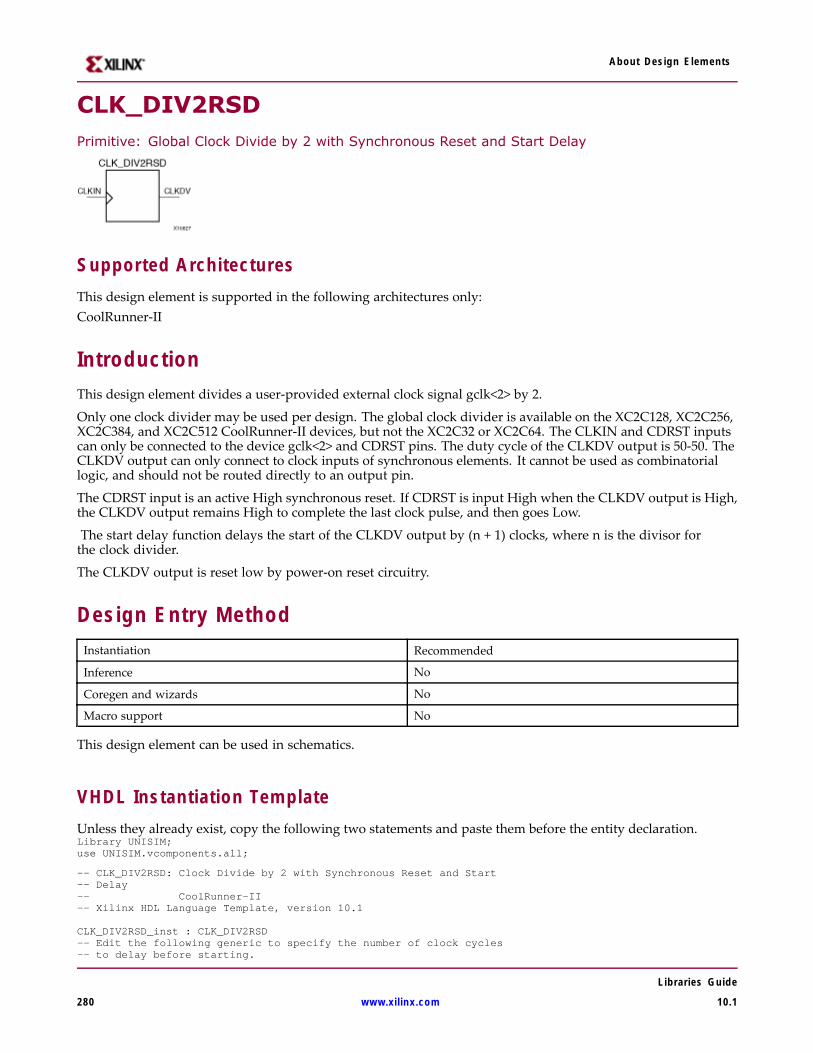
About Design Elements
CLK_DIV2RSDPrimitive: Global Clock Divide by 2 with Synchronous Reset and Start Delay
Supported ArchitecturesThis design element is supported in the following architectures only:CoolRunner-II
IntroductionThis design element divides a user-provided external clock signal gclk<2> by 2.
Only one clock divider may be used per design. The global clock divider is available on the XC2C128, XC2C256,XC2C384, and XC2C512 CoolRunner-II devices, but not the XC2C32 or XC2C64. The CLKIN and CDRST inputscan only be connected to the device gclk<2> and CDRST pins. The duty cycle of the CLKDV output is 50-50. TheCLKDV output can only connect to clock inputs of synchronous elements. It cannot be used as combinatoriallogic, and should not be routed directly to an output pin.
The CDRST input is an active High synchronous reset. If CDRST is input High when the CLKDV output is High,the CLKDV output remains High to complete the last clock pulse, and then goes Low.
The start delay function delays the start of the CLKDV output by (n + 1) clocks, where n is the divisor forthe clock divider.
The CLKDV output is reset low by power-on reset circuitry.
Design Entry MethodInstantiation Recommended
Inference No
Coregen and wizards No
Macro support No
This design element can be used in schematics.
VHDL Instantiation TemplateUnless they already exist, copy the following two statements and paste them before the entity declaration.Library UNISIM;use UNISIM.vcomponents.all;
-- CLK_DIV2RSD: Clock Divide by 2 with Synchronous Reset and Start-- Delay-- CoolRunner-II-- Xilinx HDL Language Template, version 10.1
CLK_DIV2RSD_inst : CLK_DIV2RSD-- Edit the following generic to specify the number of clock cycles-- to delay before starting.
Libraries Guide
280 www.xilinx.com 10.1

About Design Elements
generic map (DIVIDER_DELAY => 1)port map (CLKDV => CLKDV, -- Divided clock outputCDRST => CDRST, -- Synchronous reset inputCLKIN => CLKIN -- Clock input);
-- End of CLK_DIV2RSD_inst instantiation
Verilog Instantiation Template// CLK_DIV2RSD: Clock Divide by 2 with Synchronous Reset and Start// Delay// CoolRunner-II// Xilinx HDL Language Template, version 10.1
CLK_DIV2RSD CLK_DIV2RSD_inst (.CLKDV(CLKDV), // Divided clock output.CDRST(CDRST), // Synchronous reset input.CLKIN(CLKIN) // Clock input);
// Edit the following defparam to specify the number of clock// cycles to delay before starting. If the instance name to// the clock divider is changed, that change needs to be// reflected in the defparam statements.
defparam CLK_DIV2RSD_inst.DIVIDER_DELAY = 1;
// End of CLK_DIV2RSD_inst instantiation
For More Information• See the appropriate CPLD User Guide.
• See the appropriate CPLD Data Sheets.
Libraries Guide
10.1 www.xilinx.com 281

About Design Elements
CLK_DIV2SDPrimitive: Global Clock Divide by 2 with Start Delay
Supported ArchitecturesThis design element is supported in the following architectures only:CoolRunner-II
IntroductionThis design element divides a user-provided external clock signal gclk<2> by 2.
Only one clock divider may be used per design. The global clock divider is available on the XC2C128, XC2C256,XC2C384, and XC2C512 CoolRunner-II devices, but not the XC2C32 or XC2C64. The CLKIN input can onlybe connected to the device gclk<2> pin. The duty cycle of the CLKDV output is 50-50. The CLKDV output canonly connect to clock inputs of synchronous elements. It cannot be used as combinatorial logic, and shouldnot be routed directly to an output pin.
The start delay function delays the start of the CLKDV output by (n + 1) clocks, where n is the divisor forthe clock divider.
The CLKDV output is reset low by power-on reset circuitry.
Design Entry MethodInstantiation Recommended
Inference No
Coregen and wizards No
Macro support No
This design element can be used in schematics.
VHDL Instantiation TemplateUnless they already exist, copy the following two statements and paste them before the entity declaration.Library UNISIM;use UNISIM.vcomponents.all;
-- CLK_DIV2SD: Clock Divide by 2 with Start Delay-- CoolRunner-II-- Xilinx HDL Language Template, version 10.1
CLK_DIV2SD_inst : CLK_DIV2SD-- Edit the following generic to specify the number of clock cycles-- to delay before starting.generic map (DIVIDER_DELAY => 1)port map (CLKDV => CLKDV, -- Divided clock output
Libraries Guide
282 www.xilinx.com 10.1

About Design Elements
CLKIN => CLKIN -- Clock input);
-- End of CLK_DIV2SD_inst instantiation
Verilog Instantiation Template// CLK_DIV2SD: Clock Divide by 2 with Start Delay// CoolRunner-II// Xilinx HDL Language Template, version 10.1
CLK_DIV2SD CLK_DIV2SD_inst (.CLKDV(CLKDV), // Divided clock output.CDRST(CDRST), // Synchronous reset input.CLKIN(CLKIN) // Clock input);
// Edit the following defparam to specify the number of clock// cycles to delay before starting. If the instance name to// the clock divider is changed, that change needs to be// reflected in the defparam statements.
defparam CLK_DIV2SD_inst.DIVIDER_DELAY = 1;
// End of CLK_DIV2SD_inst instantiation
For More Information• See the appropriate CPLD User Guide.
• See the appropriate CPLD Data Sheets.
Libraries Guide
10.1 www.xilinx.com 283

About Design Elements
CLK_DIV4Primitive: Simple Global Clock Divide by 4
Supported ArchitecturesThis design element is supported in the following architectures only:CoolRunner-II
IntroductionThis design element divides a user-provided external clock signal gclk<2> by 4.
Only one clock divider may be used per design. The global clock divider is available on the XC2C128, XC2C256,XC2C384, and XC2C512 CoolRunner-II devices, but not the XC2C32 or XC2C64. The CLKIN input can onlybe connected to the device gclk<2> pin. The duty cycle of the CLKDV output is 50-50. The CLKDV output canonly connect to clock inputs of synchronous elements. It cannot be used as combinatorial logic, and shouldnot be routed directly to an output pin.
The CLKDV output is reset low by power-on reset circuitry.
Design Entry MethodInstantiation Recommended
Inference No
Coregen and wizards No
Macro support No
This design element can be used in schematics.
VHDL Instantiation TemplateUnless they already exist, copy the following two statements and paste them before the entity declaration.Library UNISIM;use UNISIM.vcomponents.all;
-- CLK_DIV4: Simple Clock Divide by 4-- CoolRunner-II-- Xilinx HDL Language Template, version 10.1
CLK_DIV4_inst : CLK_DIV4port map (CLKDV => CLKDV, -- Divided clock outputCLKIN => CLKIN -- Clock input);
-- End of CLK_DIV4_inst instantiation
Libraries Guide
284 www.xilinx.com 10.1

About Design Elements
Verilog Instantiation Template// CLK_DIV4: Simple Clock Divide by 4// CoolRunner-II// Xilinx HDL Language Template, version 10.1
CLK_DIV4 CLK_DIV4_inst (.CLKDV(CLKDV), // Divided clock output.CLKIN(CLKIN) // Clock input);
// End of CLK_DIV4_inst instantiation
For More Information• See the appropriate CPLD User Guide.
• See the appropriate CPLD Data Sheets.
Libraries Guide
10.1 www.xilinx.com 285
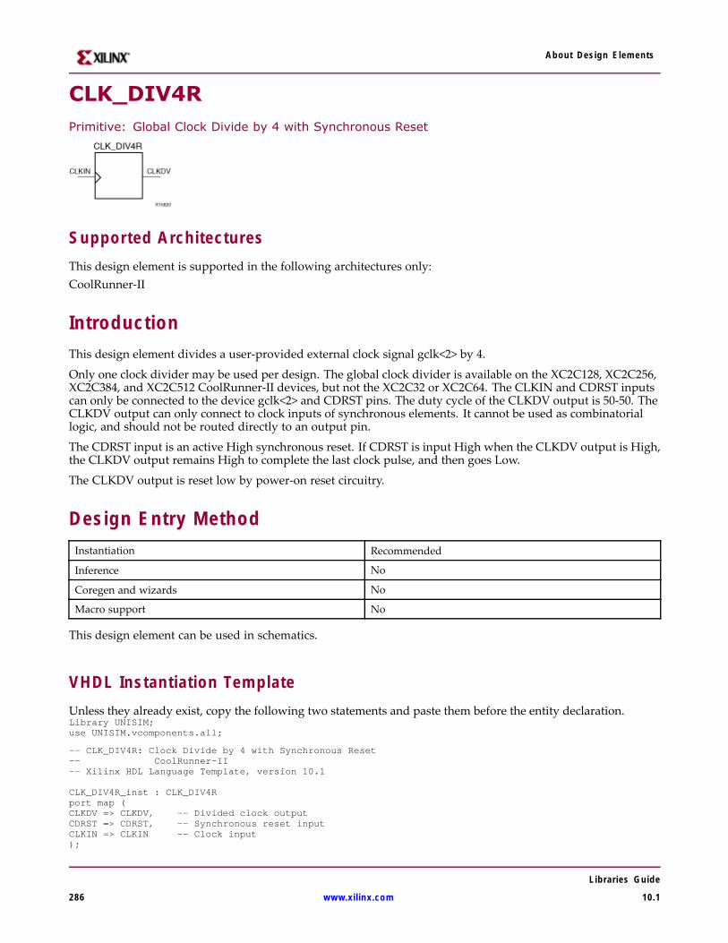
About Design Elements
CLK_DIV4RPrimitive: Global Clock Divide by 4 with Synchronous Reset
Supported ArchitecturesThis design element is supported in the following architectures only:CoolRunner-II
IntroductionThis design element divides a user-provided external clock signal gclk<2> by 4.
Only one clock divider may be used per design. The global clock divider is available on the XC2C128, XC2C256,XC2C384, and XC2C512 CoolRunner-II devices, but not the XC2C32 or XC2C64. The CLKIN and CDRST inputscan only be connected to the device gclk<2> and CDRST pins. The duty cycle of the CLKDV output is 50-50. TheCLKDV output can only connect to clock inputs of synchronous elements. It cannot be used as combinatoriallogic, and should not be routed directly to an output pin.
The CDRST input is an active High synchronous reset. If CDRST is input High when the CLKDV output is High,the CLKDV output remains High to complete the last clock pulse, and then goes Low.
The CLKDV output is reset low by power-on reset circuitry.
Design Entry MethodInstantiation Recommended
Inference No
Coregen and wizards No
Macro support No
This design element can be used in schematics.
VHDL Instantiation TemplateUnless they already exist, copy the following two statements and paste them before the entity declaration.Library UNISIM;use UNISIM.vcomponents.all;
-- CLK_DIV4R: Clock Divide by 4 with Synchronous Reset-- CoolRunner-II-- Xilinx HDL Language Template, version 10.1
CLK_DIV4R_inst : CLK_DIV4Rport map (CLKDV => CLKDV, -- Divided clock outputCDRST => CDRST, -- Synchronous reset inputCLKIN => CLKIN -- Clock input);
Libraries Guide
286 www.xilinx.com 10.1

About Design Elements
-- End of CLK_DIV4R_inst instantiation
Verilog Instantiation Template// CLK_DIV4R: Clock Divide by 4 with Synchronous Reset// CoolRunner-II// Xilinx HDL Language Template, version 10.1
CLK_DIV4R CLK_DIV4R_inst (.CLKDV(CLKDV), // Divided clock output.CDRST(CDRST), // Synchronous reset input.CLKIN(CLKIN) // Clock input);
// End of CLK_DIV4R_inst instantiation
For More Information• See the appropriate CPLD User Guide.
• See the appropriate CPLD Data Sheets.
Libraries Guide
10.1 www.xilinx.com 287

About Design Elements
CLK_DIV4RSDPrimitive: Global Clock Divide by 4 with Synchronous Reset and Start Delay
Supported ArchitecturesThis design element is supported in the following architectures only:CoolRunner-II
IntroductionThis design element divides a user-provided external clock signal gclk<2> by 4.
Only one clock divider may be used per design. The global clock divider is available on the XC2C128, XC2C256,XC2C384, and XC2C512 CoolRunner-II devices, but not the XC2C32 or XC2C64. The CLKIN and CDRST inputscan only be connected to the device gclk<2> and CDRST pins. The duty cycle of the CLKDV output is 50-50. TheCLKDV output can only connect to clock inputs of synchronous elements. It cannot be used as combinatoriallogic, and should not be routed directly to an output pin.
The CDRST input is an active High synchronous reset. If CDRST is input High when the CLKDV output is High,the CLKDV output remains High to complete the last clock pulse, and then goes Low.
The start delay function delays the start of the CLKDV output by (n + 1) clocks, where n is the divisor forthe clock divider.
The CLKDV output is reset low by power-on reset circuitry.
Design Entry MethodInstantiation Recommended
Inference No
Coregen and wizards No
Macro support No
This design element can be used in schematics.
VHDL Instantiation TemplateUnless they already exist, copy the following two statements and paste them before the entity declaration.Library UNISIM;use UNISIM.vcomponents.all;
-- CLK_DIV4RSD: Clock Divide by 4 with Synchronous Reset and Start-- Delay-- CoolRunner-II-- Xilinx HDL Language Template, version 10.1
CLK_DIV4RSD_inst : CLK_DIV4RSD-- Edit the following generic to specify the number of clock cycles-- to delay before starting.
Libraries Guide
288 www.xilinx.com 10.1

About Design Elements
generic map (DIVIDER_DELAY => 1)port map (CLKDV => CLKDV, -- Divided clock outputCDRST => CDRST, -- Synchronous reset inputCLKIN => CLKIN -- Clock input);
-- End of CLK_DIV4RSD_inst instantiation
Verilog Instantiation Template// CLK_DIV4RSD: Clock Divide by 4 with Synchronous Reset and Start// Delay// CoolRunner-II// Xilinx HDL Language Template, version 10.1
CLK_DIV4RSD CLK_DIV4RSD_inst (.CLKDV(CLKDV), // Divided clock output.CDRST(CDRST), // Synchronous reset input.CLKIN(CLKIN) // Clock input);
// Edit the following defparam to specify the number of clock// cycles to delay before starting. If the instance name to// the clock divider is changed, that change needs to be// reflected in the defparam statements.
defparam CLK_DIV4RSD_inst.DIVIDER_DELAY = 1;
// End of CLK_DIV4RSD_inst instantiation
For More Information• See the appropriate CPLD User Guide.
• See the appropriate CPLD Data Sheets.
Libraries Guide
10.1 www.xilinx.com 289

About Design Elements
CLK_DIV4SDPrimitive: Global Clock Divide by 4 with Start Delay
Supported ArchitecturesThis design element is supported in the following architectures only:CoolRunner-II
IntroductionThis design element divides a user-provided external clock signal gclk<2> by 4.
Only one clock divider may be used per design. The global clock divider is available on the XC2C128, XC2C256,XC2C384, and XC2C512 CoolRunner-II devices, but not the XC2C32 or XC2C64. The CLKIN input can onlybe connected to the device gclk<2> pin. The duty cycle of the CLKDV output is 50-50. The CLKDV output canonly connect to clock inputs of synchronous elements. It cannot be used as combinatorial logic, and shouldnot be routed directly to an output pin.
The start delay function delays the start of the CLKDV output by (n + 1) clocks, where n is the divisor forthe clock divider.
The CLKDV output is reset low by power-on reset circuitry.
Design Entry MethodInstantiation Recommended
Inference No
Coregen and wizards No
Macro support No
This design element can be used in schematics.
VHDL Instantiation TemplateUnless they already exist, copy the following two statements and paste them before the entity declaration.Library UNISIM;use UNISIM.vcomponents.all;
-- CLK_DIV4SD: Clock Divide by 4 with Start Delay-- CoolRunner-II-- Xilinx HDL Language Template, version 10.1
CLK_DIV4SD_inst : CLK_DIV4SD-- Edit the following generic to specify the number of clock cycles-- to delay before starting.generic map (DIVIDER_DELAY => 1)port map (CLKDV => CLKDV, -- Divided clock output
Libraries Guide
290 www.xilinx.com 10.1

About Design Elements
CLKIN => CLKIN -- Clock input);
-- End of CLK_DIV4SD_inst instantiation
Verilog Instantiation Template// CLK_DIV4SD: Clock Divide by 4 with Start Delay// CoolRunner-II// Xilinx HDL Language Template, version 10.1
CLK_DIV4SD CLK_DIV4SD_inst (.CLKDV(CLKDV), // Divided clock output.CDRST(CDRST), // Synchronous reset input.CLKIN(CLKIN) // Clock input);
// Edit the following defparam to specify the number of clock// cycles to delay before starting. If the instance name to// the clock divider is changed, that change needs to be// reflected in the defparam statements.
defparam CLK_DIV4SD_inst.DIVIDER_DELAY = 1;
// End of CLK_DIV4SD_inst instantiation
For More Information• See the appropriate CPLD User Guide.
• See the appropriate CPLD Data Sheets.
Libraries Guide
10.1 www.xilinx.com 291

About Design Elements
CLK_DIV6Primitive: Simple Global Clock Divide by 6
Supported ArchitecturesThis design element is supported in the following architectures only:CoolRunner-II
IntroductionThis design element divides a user-provided external clock signal gclk<2> by 6.
Only one clock divider may be used per design. The global clock divider is available on the XC2C128, XC2C256,XC2C384, and XC2C512 CoolRunner-II devices, but not the XC2C32 or XC2C64. The CLKIN input can onlybe connected to the device gclk<2> pin. The duty cycle of the CLKDV output is 50-50. The CLKDV output canonly connect to clock inputs of synchronous elements. It cannot be used as combinatorial logic, and shouldnot be routed directly to an output pin.
The CLKDV output is reset low by power-on reset circuitry.
Design Entry MethodInstantiation Recommended
Inference No
Coregen and wizards No
Macro support No
This design element can be used in schematics.
VHDL Instantiation TemplateUnless they already exist, copy the following two statements and paste them before the entity declaration.Library UNISIM;use UNISIM.vcomponents.all;
-- CLK_DIV6: Simple Clock Divide by 6-- CoolRunner-II-- Xilinx HDL Language Template, version 10.1
CLK_DIV6_inst : CLK_DIV6port map (CLKDV => CLKDV, -- Divided clock outputCLKIN => CLKIN -- Clock input);
-- End of CLK_DIV6_inst instantiation
Libraries Guide
292 www.xilinx.com 10.1

About Design Elements
Verilog Instantiation Template// CLK_DIV6: Simple Clock Divide by 6// CoolRunner-II// Xilinx HDL Language Template, version 10.1
CLK_DIV6 CLK_DIV6_inst (.CLKDV(CLKDV), // Divided clock output.CLKIN(CLKIN) // Clock input);
// End of CLK_DIV6_inst instantiation
For More Information• See the appropriate CPLD User Guide.
• See the appropriate CPLD Data Sheets.
Libraries Guide
10.1 www.xilinx.com 293

About Design Elements
CLK_DIV6RPrimitive: Global Clock Divide by 6 with Synchronous Reset
Supported ArchitecturesThis design element is supported in the following architectures only:CoolRunner-II
IntroductionThis design element divides a user-provided external clock signal gclk<2> by 6.
Only one clock divider may be used per design. The global clock divider is available on the XC2C128, XC2C256,XC2C384, and XC2C512 CoolRunner-II devices, but not the XC2C32 or XC2C64. The CLKIN and CDRST inputscan only be connected to the device gclk<2> and CDRST pins. The duty cycle of the CLKDV output is 50-50. TheCLKDV output can only connect to clock inputs of synchronous elements. It cannot be used as combinatoriallogic, and should not be routed directly to an output pin.
The CDRST input is an active High synchronous reset. If CDRST is input High when the CLKDV output is High,the CLKDV output remains High to complete the last clock pulse, and then goes Low.
The CLKDV output is reset low by power-on reset circuitry.
Design Entry MethodInstantiation Recommended
Inference No
Coregen and wizards No
Macro support No
This design element can be used in schematics.
VHDL Instantiation TemplateUnless they already exist, copy the following two statements and paste them before the entity declaration.Library UNISIM;use UNISIM.vcomponents.all;
-- CLK_DIV6R: Clock Divide by 6 with Synchronous Reset-- CoolRunner-II-- Xilinx HDL Language Template, version 10.1
CLK_DIV6R_inst : CLK_DIV6Rport map (CLKDV => CLKDV, -- Divided clock outputCDRST => CDRST, -- Synchronous reset inputCLKIN => CLKIN -- Clock input);
Libraries Guide
294 www.xilinx.com 10.1

About Design Elements
-- End of CLK_DIV6R_inst instantiation
Verilog Instantiation Template// CLK_DIV6R: Clock Divide by 6 with Synchronous Reset// CoolRunner-II// Xilinx HDL Language Template, version 10.1
CLK_DIV6R CLK_DIV6R_inst (.CLKDV(CLKDV), // Divided clock output.CDRST(CDRST), // Synchronous reset input.CLKIN(CLKIN) // Clock input);
// End of CLK_DIV6R_inst instantiation
For More Information• See the appropriate CPLD User Guide.
• See the appropriate CPLD Data Sheets.
Libraries Guide
10.1 www.xilinx.com 295

About Design Elements
CLK_DIV6RSDPrimitive: Global Clock Divide by 6 with Synchronous Reset and Start Delay
Supported ArchitecturesThis design element is supported in the following architectures only:CoolRunner-II
IntroductionThis design element divides a user-provided external clock signal gclk<2> by 6.
Only one clock divider may be used per design. The global clock divider is available on the XC2C128, XC2C256,XC2C384, and XC2C512 CoolRunner-II devices, but not the XC2C32 or XC2C64. The CLKIN and CDRST inputscan only be connected to the device gclk<2> and CDRST pins. The duty cycle of the CLKDV output is 50-50. TheCLKDV output can only connect to clock inputs of synchronous elements. It cannot be used as combinatoriallogic, and should not be routed directly to an output pin.
The CDRST input is an active High synchronous reset. If CDRST is input High when the CLKDV output is High,the CLKDV output remains High to complete the last clock pulse, and then goes Low.
The start delay function delays the start of the CLKDV output by (n + 1) clocks, where n is the divisor forthe clock divider.
The CLKDV output is reset low by power-on reset circuitry.
Design Entry MethodInstantiation Recommended
Inference No
Coregen and wizards No
Macro support No
This design element can be used in schematics.
VHDL Instantiation TemplateUnless they already exist, copy the following two statements and paste them before the entity declaration.Library UNISIM;use UNISIM.vcomponents.all;
-- CLK_DIV6RSD: Clock Divide by 6 with Synchronous Reset and Start-- Delay-- CoolRunner-II-- Xilinx HDL Language Template, version 10.1
CLK_DIV6RSD_inst : CLK_DIV6RSD-- Edit the following generic to specify the number of clock cycles-- to delay before starting.
Libraries Guide
296 www.xilinx.com 10.1

About Design Elements
generic map (DIVIDER_DELAY => 1)port map (CLKDV => CLKDV, -- Divided clock outputCDRST => CDRST, -- Synchronous reset inputCLKIN => CLKIN -- Clock input);
-- End of CLK_DIV6RSD_inst instantiation
Verilog Instantiation Template// CLK_DIV6RSD: Clock Divide by 6 with Synchronous Reset and Start// Delay// CoolRunner-II// Xilinx HDL Language Template, version 10.1
CLK_DIV6RSD CLK_DIV6RSD_inst (.CLKDV(CLKDV), // Divided clock output.CDRST(CDRST), // Synchronous reset input.CLKIN(CLKIN) // Clock input);
// Edit the following defparam to specify the number of clock// cycles to delay before starting. If the instance name to// the clock divider is changed, that change needs to be// reflected in the defparam statements.
defparam CLK_DIV6RSD_inst.DIVIDER_DELAY = 1;
// End of CLK_DIV6RSD_inst instantiation
For More Information• See the appropriate CPLD User Guide.
• See the appropriate CPLD Data Sheets.
Libraries Guide
10.1 www.xilinx.com 297
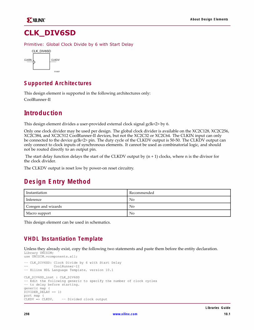
About Design Elements
CLK_DIV6SDPrimitive: Global Clock Divide by 6 with Start Delay
Supported ArchitecturesThis design element is supported in the following architectures only:CoolRunner-II
IntroductionThis design element divides a user-provided external clock signal gclk<2> by 6.
Only one clock divider may be used per design. The global clock divider is available on the XC2C128, XC2C256,XC2C384, and XC2C512 CoolRunner-II devices, but not the XC2C32 or XC2C64. The CLKIN input can onlybe connected to the device gclk<2> pin. The duty cycle of the CLKDV output is 50-50. The CLKDV output canonly connect to clock inputs of synchronous elements. It cannot be used as combinatorial logic, and shouldnot be routed directly to an output pin.
The start delay function delays the start of the CLKDV output by (n + 1) clocks, where n is the divisor forthe clock divider.
The CLKDV output is reset low by power-on reset circuitry.
Design Entry MethodInstantiation Recommended
Inference No
Coregen and wizards No
Macro support No
This design element can be used in schematics.
VHDL Instantiation TemplateUnless they already exist, copy the following two statements and paste them before the entity declaration.Library UNISIM;use UNISIM.vcomponents.all;
-- CLK_DIV6SD: Clock Divide by 6 with Start Delay-- CoolRunner-II-- Xilinx HDL Language Template, version 10.1
CLK_DIV6SD_inst : CLK_DIV6SD-- Edit the following generic to specify the number of clock cycles-- to delay before starting.generic map (DIVIDER_DELAY => 1)port map (CLKDV => CLKDV, -- Divided clock output
Libraries Guide
298 www.xilinx.com 10.1

About Design Elements
CLKIN => CLKIN -- Clock input);
-- End of CLK_DIV4SD_inst instantiation
Verilog Instantiation Template// CLK_DIV6SD: Clock Divide by 6 with Start Delay// CoolRunner-II// Xilinx HDL Language Template, version 10.1
CLK_DIV6SD CLK_DIV6SD_inst (.CLKDV(CLKDV), // Divided clock output.CDRST(CDRST), // Synchronous reset input.CLKIN(CLKIN) // Clock input);
// Edit the following defparam to specify the number of clock// cycles to delay before starting. If the instance name to// the clock divider is changed, that change needs to be// reflected in the defparam statements.
defparam CLK_DIV6SD_inst.DIVIDER_DELAY = 1;
// End of CLK_DIV6SD_inst instantiation
For More Information• See the appropriate CPLD User Guide.
• See the appropriate CPLD Data Sheets.
Libraries Guide
10.1 www.xilinx.com 299
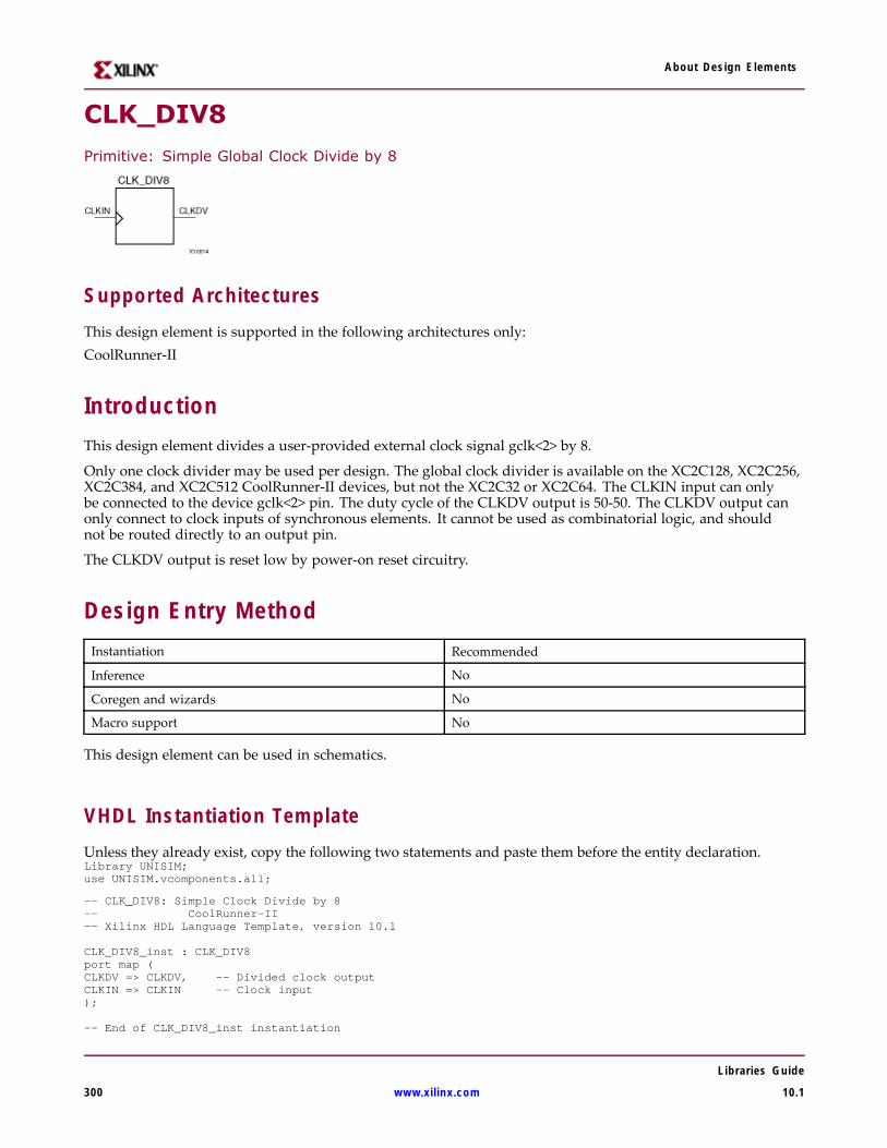
About Design Elements
CLK_DIV8
Primitive: Simple Global Clock Divide by 8
Supported ArchitecturesThis design element is supported in the following architectures only:CoolRunner-II
IntroductionThis design element divides a user-provided external clock signal gclk<2> by 8.
Only one clock divider may be used per design. The global clock divider is available on the XC2C128, XC2C256,XC2C384, and XC2C512 CoolRunner-II devices, but not the XC2C32 or XC2C64. The CLKIN input can onlybe connected to the device gclk<2> pin. The duty cycle of the CLKDV output is 50-50. The CLKDV output canonly connect to clock inputs of synchronous elements. It cannot be used as combinatorial logic, and shouldnot be routed directly to an output pin.
The CLKDV output is reset low by power-on reset circuitry.
Design Entry MethodInstantiation Recommended
Inference No
Coregen and wizards No
Macro support No
This design element can be used in schematics.
VHDL Instantiation TemplateUnless they already exist, copy the following two statements and paste them before the entity declaration.Library UNISIM;use UNISIM.vcomponents.all;
-- CLK_DIV8: Simple Clock Divide by 8-- CoolRunner-II-- Xilinx HDL Language Template, version 10.1
CLK_DIV8_inst : CLK_DIV8port map (CLKDV => CLKDV, -- Divided clock outputCLKIN => CLKIN -- Clock input);
-- End of CLK_DIV8_inst instantiation
Libraries Guide
300 www.xilinx.com 10.1
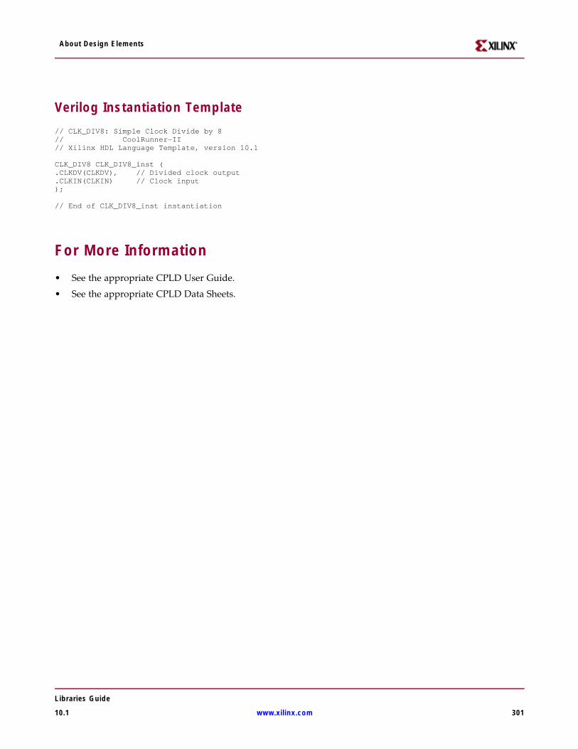
About Design Elements
Verilog Instantiation Template// CLK_DIV8: Simple Clock Divide by 8// CoolRunner-II// Xilinx HDL Language Template, version 10.1
CLK_DIV8 CLK_DIV8_inst (.CLKDV(CLKDV), // Divided clock output.CLKIN(CLKIN) // Clock input);
// End of CLK_DIV8_inst instantiation
For More Information• See the appropriate CPLD User Guide.
• See the appropriate CPLD Data Sheets.
Libraries Guide
10.1 www.xilinx.com 301

About Design Elements
CLK_DIV8RPrimitive: Global Clock Divide by 8 with Synchronous Reset
Supported ArchitecturesThis design element is supported in the following architectures only:CoolRunner-II
IntroductionThis design element divides a user-provided external clock signal gclk<2> by 8.
Only one clock divider may be used per design. The global clock divider is available on the XC2C128, XC2C256,XC2C384, and XC2C512 CoolRunner-II devices, but not the XC2C32 or XC2C64. The CLKIN and CDRST inputscan only be connected to the device gclk<2> and CDRST pins. The duty cycle of the CLKDV output is 50-50. TheCLKDV output can only connect to clock inputs of synchronous elements. It cannot be used as combinatoriallogic, and should not be routed directly to an output pin.
The CDRST input is an active High synchronous reset. If CDRST is input High when the CLKDV output is High,the CLKDV output remains High to complete the last clock pulse, and then goes Low.
The CLKDV output is reset low by power-on reset circuitry.
Design Entry MethodInstantiation Recommended
Inference No
Coregen and wizards No
Macro support No
This design element can be used in schematics.
VHDL Instantiation TemplateUnless they already exist, copy the following two statements and paste them before the entity declaration.Library UNISIM;use UNISIM.vcomponents.all;
-- CLK_DIV8R: Clock Divide by 8 with Synchronous Reset-- CoolRunner-II-- Xilinx HDL Language Template, version 10.1
CLK_DIV8R_inst : CLK_DIV8Rport map (CLKDV => CLKDV, -- Divided clock outputCDRST => CDRST, -- Synchronous reset inputCLKIN => CLKIN -- Clock input);
Libraries Guide
302 www.xilinx.com 10.1

About Design Elements
-- End of CLK_DIV8R_inst instantiation
Verilog Instantiation Template// CLK_DIV8R: Clock Divide by 8 with Synchronous Reset// CoolRunner-II// Xilinx HDL Language Template, version 10.1
CLK_DIV8R CLK_DIV8R_inst (.CLKDV(CLKDV), // Divided clock output.CDRST(CDRST), // Synchronous reset input.CLKIN(CLKIN) // Clock input);
// End of CLK_DIV8R_inst instantiation
For More Information• See the appropriate CPLD User Guide.
• See the appropriate CPLD Data Sheets.
Libraries Guide
10.1 www.xilinx.com 303

About Design Elements
CLK_DIV8RSDPrimitive: Global Clock Divide by 8 with Synchronous Reset and Start Delay
Supported ArchitecturesThis design element is supported in the following architectures only:CoolRunner-II
IntroductionThis design element divides a user-provided external clock signal gclk<2> by 8.
Only one clock divider may be used per design. The global clock divider is available on the XC2C128, XC2C256,XC2C384, and XC2C512 CoolRunner-II devices, but not the XC2C32 or XC2C64. The CLKIN and CDRST inputscan only be connected to the device gclk<2> and CDRST pins. The duty cycle of the CLKDV output is 50-50. TheCLKDV output can only connect to clock inputs of synchronous elements. It cannot be used as combinatoriallogic, and should not be routed directly to an output pin.
The CDRST input is an active High synchronous reset. If CDRST is input High when the CLKDV output is High,the CLKDV output remains High to complete the last clock pulse, and then goes Low.
The start delay function delays the start of the CLKDV output by (n + 1) clocks, where n is the divisor forthe clock divider.
The CLKDV output is reset low by power-on reset circuitry.
Design Entry MethodInstantiation Recommended
Inference No
Coregen and wizards No
Macro support No
This design element can be used in schematics.
VHDL Instantiation TemplateUnless they already exist, copy the following two statements and paste them before the entity declaration.Library UNISIM;use UNISIM.vcomponents.all;
-- CLK_DIV8RSD: Clock Divide by 8 with Synchronous Reset and Start-- Delay-- CoolRunner-II-- Xilinx HDL Language Template, version 10.1
CLK_DIV8RSD_inst : CLK_DIV8RSD-- Edit the following generic to specify the number of clock cycles-- to delay before starting.
Libraries Guide
304 www.xilinx.com 10.1

About Design Elements
generic map (DIVIDER_DELAY => 1)port map (CLKDV => CLKDV, -- Divided clock outputCDRST => CDRST, -- Synchronous reset inputCLKIN => CLKIN -- Clock input);
-- End of CLK_DIV8RSD_inst instantiation
Verilog Instantiation Template// CLK_DIV8RSD: Clock Divide by 8 with Synchronous Reset and Start// Delay// CoolRunner-II// Xilinx HDL Language Template, version 10.1
CLK_DIV8RSD CLK_DIV8RSD_inst (.CLKDV(CLKDV), // Divided clock output.CDRST(CDRST), // Synchronous reset input.CLKIN(CLKIN) // Clock input);
// Edit the following defparam to specify the number of clock// cycles to delay before starting. If the instance name to// the clock divider is changed, that change needs to be// reflected in the defparam statements.
defparam CLK_DIV8RSD_inst.DIVIDER_DELAY = 1;
// End of CLK_DIV8RSD_inst instantiation
For More Information• See the appropriate CPLD User Guide.
• See the appropriate CPLD Data Sheets.
Libraries Guide
10.1 www.xilinx.com 305

About Design Elements
CLK_DIV8SDPrimitive: Global Clock Divide by 8 with Start Delay
Supported ArchitecturesThis design element is supported in the following architectures only:CoolRunner-II
IntroductionThis design element divides a user-provided external clock signal gclk<2> by 8.
Only one clock divider may be used per design. The global clock divider is available on the XC2C128, XC2C256,XC2C384, and XC2C512 CoolRunner-II devices, but not the XC2C32 or XC2C64. The CLKIN input can onlybe connected to the device gclk<2> pin. The duty cycle of the CLKDV output is 50-50. The CLKDV output canonly connect to clock inputs of synchronous elements. It cannot be used as combinatorial logic, and shouldnot be routed directly to an output pin.
The start delay function delays the start of the CLKDV output by (n + 1) clocks, where n is the divisor forthe clock divider.
The CLKDV output is reset low by power-on reset circuitry.
Design Entry MethodInstantiation Recommended
Inference No
Coregen and wizards No
Macro support No
This design element can be used in schematics.
VHDL Instantiation TemplateUnless they already exist, copy the following two statements and paste them before the entity declaration.Library UNISIM;use UNISIM.vcomponents.all;
-- CLK_DIV8SD: Clock Divide by 8 with Start Delay-- CoolRunner-II-- Xilinx HDL Language Template, version 10.1
CLK_DIV8SD_inst : CLK_DIV8SD-- Edit the following generic to specify the number of clock cycles-- to delay before starting.generic map (DIVIDER_DELAY => 1)port map (CLKDV => CLKDV, -- Divided clock output
Libraries Guide
306 www.xilinx.com 10.1

About Design Elements
CLKIN => CLKIN -- Clock input);
-- End of CLK_DIV8SD_inst instantiation
Verilog Instantiation Template// CLK_DIV8SD: Clock Divide by 8 with Start Delay// CoolRunner-II// Xilinx HDL Language Template, version 10.1
CLK_DIV8SD CLK_DIV8SD_inst (.CLKDV(CLKDV), // Divided clock output.CDRST(CDRST), // Synchronous reset input.CLKIN(CLKIN) // Clock input);
// Edit the following defparam to specify the number of clock// cycles to delay before starting. If the instance name to// the clock divider is changed, that change needs to be// reflected in the defparam statements.
defparam CLK_DIV8SD_inst.DIVIDER_DELAY = 1;
// End of CLK_DIV8SD_inst instantiation
For More Information• See the appropriate CPLD User Guide.
• See the appropriate CPLD Data Sheets.
Libraries Guide
10.1 www.xilinx.com 307

About Design Elements
COMP16
Macro: 16-Bit Identity Comparator
Supported Architectures
This design element is supported in the following architectures only:
• XC9500XL
• CoolRunner XPLA3
• CoolRunner-II
IntroductionThis design element is a 16-bit identity comparator. The equal output (EQ) is high when A15 – A0 and B15 –B0 are equal.
Equality is determined by a bit comparison of the two words. When any two of the corresponding bits fromeach word are not the same, the EQ output is Low.
Design Entry MethodThis design element is only for use in schematics.
For More Information• See the appropriate CPLD User Guide.
• See the appropriate CPLD Data Sheets.
Libraries Guide
308 www.xilinx.com 10.1

About Design Elements
COMP2
Macro: 2-Bit Identity Comparator
Supported Architectures
This design element is supported in the following architectures only:
• XC9500XL
• CoolRunner XPLA3
• CoolRunner-II
IntroductionThis design element is a 2-bit identity comparator. The equal output (EQ) is High when the two words A1 – A0and B1 – B0 are equal.
Equality is determined by a bit comparison of the two words. When any two of the corresponding bits fromeach word are not the same, the EQ output is Low.
Design Entry MethodThis design element is only for use in schematics.
For More Information• See the appropriate CPLD User Guide.
• See the appropriate CPLD Data Sheets.
Libraries Guide
10.1 www.xilinx.com 309

About Design Elements
COMP4
Macro: 4-Bit Identity Comparator
Supported Architectures
This design element is supported in the following architectures only:
• XC9500XL
• CoolRunner XPLA3
• CoolRunner-II
IntroductionThis design element is a 4-bit identity comparator. The equal output (EQ) is high when A3 – A0 and B3 –B0 are equal.
Equality is determined by a bit comparison of the two words. When any two of the corresponding bits fromeach word are not the same, the EQ output is Low.
Design Entry MethodThis design element is only for use in schematics.
For More Information• See the appropriate CPLD User Guide.
• See the appropriate CPLD Data Sheets.
Libraries Guide
310 www.xilinx.com 10.1
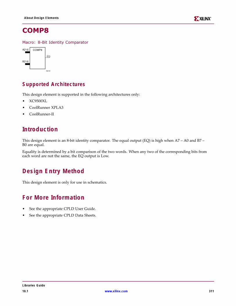
About Design Elements
COMP8
Macro: 8-Bit Identity Comparator
Supported Architectures
This design element is supported in the following architectures only:
• XC9500XL
• CoolRunner XPLA3
• CoolRunner-II
IntroductionThis design element is an 8-bit identity comparator. The equal output (EQ) is high when A7 – A0 and B7 –B0 are equal.
Equality is determined by a bit comparison of the two words. When any two of the corresponding bits fromeach word are not the same, the EQ output is Low.
Design Entry MethodThis design element is only for use in schematics.
For More Information• See the appropriate CPLD User Guide.
• See the appropriate CPLD Data Sheets.
Libraries Guide
10.1 www.xilinx.com 311

About Design Elements
COMPM16Macro: 16-Bit Magnitude Comparator
Supported ArchitecturesThis design element is supported in the following architectures only:• XC9500XL• CoolRunner XPLA3• CoolRunner-II
IntroductionThis design element is a 16-bit magnitude comparator that compare two positive Binary-weighted words. Itcompares A15 – A0 and B15 – B0, where A15 and B15 are the most significant bits.
The greater-than output (GT) is High when A > B, and the less-than output (LT) is High when A < B Whenthe two words are equal, both GT and LT are Low. Equality can be measured with this macro by comparingboth outputs with a NOR gate.
Logic TableInputs Outputs
A7, B7 A6, B6 A5, B5 A4, B4 A3, B3 A2, B2 A1, B1 A0, B0 GT LT
A7>B7 X X X X X X X 1 0
A7<B7 X X X X X X X 0 1
A7=B7 A6>B6 X X X X X X 1 0
A7=B7 A6<B6 X X X X X X 0 1
A7=B7 A6=B6 A5>B5 X X X X X 1 0
A7=B7 A6=B6 A5<B5 X X X X X 0 1
A7=B7 A6=B6 A5=B5 A4>B4 X X X X 1 0
A7=B7 A6=B6 A5=B5 A4<B4 X X X X 0 1
A7=B7 A6=B6 A5=B5 A4=B4 A3>B3 X X X 1 0
A7=B7 A6=B6 A5=B5 A4=B4 A3<B3 X X X 0 1
A7=B7 A6=B6 A5=B5 A4=B4 A3=B3 A2>B2 X X 1 0
A7=B7 A6=B6 A5=B5 A4=B4 A3=B3 A2<B2 X X 0 1
A7=B7 A6=B6 A5=B5 A4=B4 A3=B3 A2=B2 A1>B1 X 1 0
A7=B7 A6=B6 A5=B5 A4=B4 A3=B3 A2=B2 A1<B1 X 0 1
A7=B7 A6=B6 A5=B5 A4=B4 A3=B3 A2=B2 A1=B1 A0>B0 1 0
Libraries Guide
312 www.xilinx.com 10.1

About Design Elements
Inputs Outputs
A7, B7 A6, B6 A5, B5 A4, B4 A3, B3 A2, B2 A1, B1 A0, B0 GT LT
A7=B7 A6=B6 A5=B5 A4=B4 A3=B3 A2=B2 A1=B1 A0<B0 0 1
A7=B7 A6=B6 A5=B5 A4=B4 A3=B3 A2=B2 A1=B1 A0=B0 0 0
Design Entry MethodThis design element is only for use in schematics.
For More Information• See the appropriate CPLD User Guide.
• See the appropriate CPLD Data Sheets.
Libraries Guide
10.1 www.xilinx.com 313

About Design Elements
COMPM2
Macro: 2-Bit Magnitude Comparator
Supported ArchitecturesThis design element is supported in the following architectures only:• XC9500XL• CoolRunner XPLA3• CoolRunner-II
IntroductionThis design element is a 2-bit magnitude comparator that compare two positive Binary-weighted words. Itcompares A1 – A0 and B1 – B0, where A1 and B1 are the most significant bits.
The greater-than output (GT) is High when A > B, and the less-than output (LT) is High when A < B Whenthe two words are equal, both GT and LT are Low. Equality can be measured with this macro by comparingboth outputs with a NOR gate.
Logic TableInputs Outputs
A1 B1 A0 B0 GT LT
0 0 0 0 0 0
0 0 1 0 1 0
0 0 0 1 0 1
0 0 1 1 0 0
1 1 0 0 0 0
1 1 1 0 1 0
1 1 0 1 0 1
1 1 1 1 0 0
1 0 X X 1 0
0 1 X X 0 1
Design Entry MethodThis design element is only for use in schematics.
Libraries Guide
314 www.xilinx.com 10.1

About Design Elements
For More Information• See the appropriate CPLD User Guide.
• See the appropriate CPLD Data Sheets.
Libraries Guide
10.1 www.xilinx.com 315
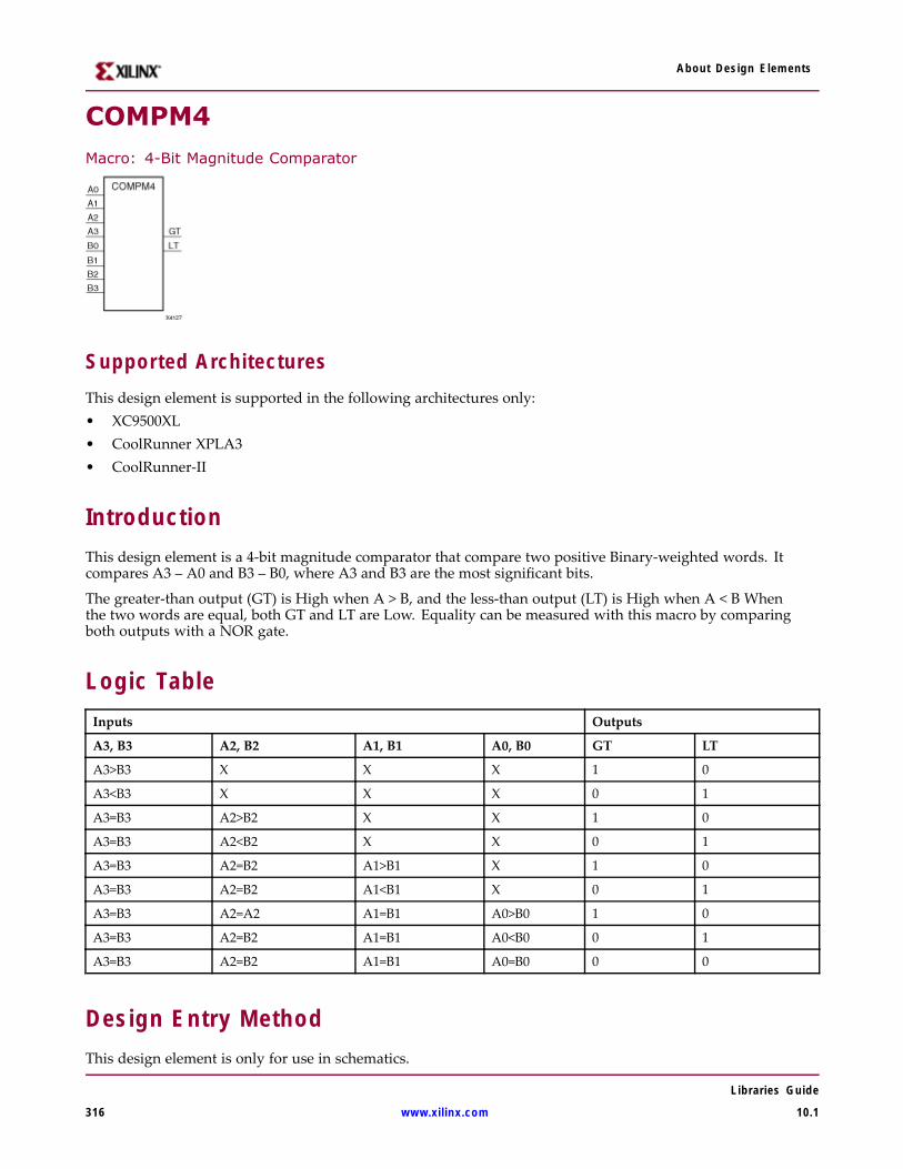
About Design Elements
COMPM4Macro: 4-Bit Magnitude Comparator
Supported ArchitecturesThis design element is supported in the following architectures only:• XC9500XL• CoolRunner XPLA3• CoolRunner-II
IntroductionThis design element is a 4-bit magnitude comparator that compare two positive Binary-weighted words. Itcompares A3 – A0 and B3 – B0, where A3 and B3 are the most significant bits.
The greater-than output (GT) is High when A > B, and the less-than output (LT) is High when A < B Whenthe two words are equal, both GT and LT are Low. Equality can be measured with this macro by comparingboth outputs with a NOR gate.
Logic TableInputs Outputs
A3, B3 A2, B2 A1, B1 A0, B0 GT LT
A3>B3 X X X 1 0
A3<B3 X X X 0 1
A3=B3 A2>B2 X X 1 0
A3=B3 A2<B2 X X 0 1
A3=B3 A2=B2 A1>B1 X 1 0
A3=B3 A2=B2 A1<B1 X 0 1
A3=B3 A2=A2 A1=B1 A0>B0 1 0
A3=B3 A2=B2 A1=B1 A0<B0 0 1
A3=B3 A2=B2 A1=B1 A0=B0 0 0
Design Entry MethodThis design element is only for use in schematics.
Libraries Guide
316 www.xilinx.com 10.1

About Design Elements
For More Information• See the appropriate CPLD User Guide.
• See the appropriate CPLD Data Sheets.
Libraries Guide
10.1 www.xilinx.com 317

About Design Elements
COMPM8Macro: 8-Bit Magnitude Comparator
Supported ArchitecturesThis design element is supported in the following architectures only:• XC9500XL• CoolRunner XPLA3• CoolRunner-II
IntroductionThis design element is an 8-bit magnitude comparator that compare two positive Binary-weighted words. Itcompares A7 – A0 and B7 – B0, where A7 and B7 are the most significant bits.
The greater-than output (GT) is High when A > B, and the less-than output (LT) is High when A < B Whenthe two words are equal, both GT and LT are Low. Equality can be measured with this macro by comparingboth outputs with a NOR gate.
Logic TableInputs Outputs
A7, B7 A6, B6 A5, B5 A4, B4 A3, B3 A2, B2 A1, B1 A0, B0 GT LT
A7>B7 X X X X X X X 1 0
A7<B7 X X X X X X X 0 1
A7=B7 A6>B6 X X X X X X 1 0
A7=B7 A6<B6 X X X X X X 0 1
A7=B7 A6=B6 A5>B5 X X X X X 1 0
A7=B7 A6=B6 A5<B5 X X X X X 0 1
A7=B7 A6=B6 A5=B5 A4>B4 X X X X 1 0
A7=B7 A6=B6 A5=B5 A4<B4 X X X X 0 1
A7=B7 A6=B6 A5=B5 A4=B4 A3>B3 X X X 1 0
A7=B7 A6=B6 A5=B5 A4=B4 A3<B3 X X X 0 1
A7=B7 A6=B6 A5=B5 A4=B4 A3=B3 A2>B2 X X 1 0
A7=B7 A6=B6 A5=B5 A4=B4 A3=B3 A2<B2 X X 0 1
A7=B7 A6=B6 A5=B5 A4=B4 A3=B3 A2=B2 A1>B1 X 1 0
A7=B7 A6=B6 A5=B5 A4=B4 A3=B3 A2=B2 A1<B1 X 0 1
A7=B7 A6=B6 A5=B5 A4=B4 A3=B3 A2=B2 A1=B1 A0>B0 1 0
Libraries Guide
318 www.xilinx.com 10.1
About Design Elements
Inputs Outputs
A7, B7 A6, B6 A5, B5 A4, B4 A3, B3 A2, B2 A1, B1 A0, B0 GT LT
A7=B7 A6=B6 A5=B5 A4=B4 A3=B3 A2=B2 A1=B1 A0<B0 0 1
A7=B7 A6=B6 A5=B5 A4=B4 A3=B3 A2=B2 A1=B1 A0=B0 0 0
Design Entry MethodThis design element is only for use in schematics.
For More Information• See the appropriate CPLD User Guide.
• See the appropriate CPLD Data Sheets.
Libraries Guide
10.1 www.xilinx.com 319

About Design Elements
CR16CE
Macro: 16-Bit Negative-Edge Binary Ripple Counter with Clock Enable and Asynchronous Clear
Supported ArchitecturesThis design element is supported in the following architectures only:• XC9500XL• CoolRunner XPLA3• CoolRunner-II
IntroductionThis design element is a 16-bit cascadable, clearable, binary ripple counter with clock enable and asynchronousclear.
Larger counters can be created by connecting the last Q output of the first stage to the clock input of the nextstage. CLR and CE inputs are connected in parallel. The clock period is not affected by the overall length of aripple counter. The overall clock-to-output propagation is n(tC - Q), where n is the number of stages and the timetC - Q is the C-to-Qz propagation delay of each stage.
This counter is asynchronously cleared, outputs Low, when power is applied.
Logic TableInputs Outputs
CLR CE C Qz – Q0
1 X X 0
0 0 X No Change
0 1 ↓ Inc
z = bit width - 1
Design Entry MethodThis design element is only for use in schematics.
For More Information• See the appropriate CPLD User Guide.• See the appropriate CPLD Data Sheets.
Libraries Guide
320 www.xilinx.com 10.1

About Design Elements
CR8CEMacro: 8-Bit Negative-Edge Binary Ripple Counter with Clock Enable and Asynchronous Clear
Supported ArchitecturesThis design element is supported in the following architectures only:• XC9500XL• CoolRunner XPLA3• CoolRunner-II
IntroductionThis design element is an 8-bit cascadable, clearable, binary, ripple counter with clock enable and asynchronousclear.
The asynchronous clear (CLR), when High, overrides all other inputs and causes the Q outputs to go to logiclevel zero. The counter increments when the clock enable input (CE) is High during the High-to-Low clock (C)transition. The counter ignores clock transitions when CE is Low.
Larger counters can be created by connecting the last Q output of the first stage to the clock input of the nextstage. CLR and CE inputs are connected in parallel. The clock period is not affected by the overall length of aripple counter. The overall clock-to-output propagation is n(tC - Q), where n is the number of stages and the timetC - Q is the C-to-Qz propagation delay of each stage.
This counter is asynchronously cleared, outputs Low, when power is applied.
Logic TableInputs Outputs
CLR CE C Qz – Q0
1 X X 0
0 0 X No Change
0 1 ↓ Inc
z = bit width - 1
Design Entry MethodThis design element is only for use in schematics.
For More Information• See the appropriate CPLD User Guide.• See the appropriate CPLD Data Sheets.
Libraries Guide
10.1 www.xilinx.com 321

About Design Elements
CRD16CE
Macro: 16-Bit Dual-Edge Triggered Binary Ripple Counter with Clock Enable and AsynchronousClear
Supported Architectures
This design element is supported in the following architectures only:
CoolRunner-II
IntroductionThis design element is a dual edge triggered 16-bit cascadable, clearable, binary ripple counter.
The asynchronous clear (CLR), when High, overrides all other inputs and causes the Q outputs to go to logiclevel zero. The counter increments when the clock enable input (CE) is High during the High-to-Low andLow-to-High clock (C) transitions. The counter ignores clock transitions when CE is Low.
Larger counters can be created by connecting the last Q output of the first stage to the clock input of the nextstage. CLR and CE inputs are connected in parallel. The clock period is not affected by the overall length of aripple counter. The overall clock-to-output propagation is n(tC - Q), where n is the number of stages and the timetC - Q is the C-to-Qz propagation delay of each stage.
This counter is asynchronously cleared, outputs Low, when power is applied. For CPLD devices, you cansimulate power-on by applying a High-level pulse on the PRLD global net.
Logic TableInputs Outputs
CLR CE C Qz – Q0
1 X X 0
0 0 X No Change
0 1 ↑ Inc
0 1 ↓ Inc
z = bit width - 1
Design Entry MethodThis design element is only for use in schematics.
Libraries Guide
322 www.xilinx.com 10.1

About Design Elements
For More Information• See the appropriate CPLD User Guide.
• See the appropriate CPLD Data Sheets.
Libraries Guide
10.1 www.xilinx.com 323

About Design Elements
CRD8CE
Macro: 8-Bit Dual-Edge Triggered Binary Ripple Counter with Clock Enable and Asynchronous Clear
Supported Architectures
This design element is supported in the following architectures only:
CoolRunner-II
IntroductionThis design element is a dual edge triggered 8-bit cascadable, clearable, binary ripple counter.
The asynchronous clear (CLR), when High, overrides all other inputs and causes the Q outputs to go to logiclevel zero. The counter increments when the clock enable input (CE) is High during the High-to-Low andLow-to-High clock (C) transitions. The counter ignores clock transitions when CE is Low.
Larger counters can be created by connecting the last Q output of the first stage to the clock input of the nextstage. CLR and CE inputs are connected in parallel. The clock period is not affected by the overall length of aripple counter. The overall clock-to-output propagation is n(tC - Q), where n is the number of stages and the timetC - Q is the C-to-Qz propagation delay of each stage.
This counter is asynchronously cleared, outputs Low, when power is applied. For CPLD devices, you cansimulate power-on by applying a High-level pulse on the PRLD global net.
Logic TableInputs Outputs
CLR CE C Qz – Q0
1 X X 0
0 0 X No Change
0 1 ↑ Inc
0 1 ↓ Inc
z = bit width - 1
Design Entry MethodThis design element is only for use in schematics.
Libraries Guide
324 www.xilinx.com 10.1

About Design Elements
For More Information• See the appropriate CPLD User Guide.
• See the appropriate CPLD Data Sheets.
Libraries Guide
10.1 www.xilinx.com 325

About Design Elements
D2_4E
Macro: 2- to 4-Line Decoder/Demultiplexer with Enable
Supported Architectures
This design element is supported in the following architectures only:
• XC9500XL
• CoolRunner XPLA3
• CoolRunner-II
IntroductionThis design element is a decoder/demultiplexer. When the enable (E) input of this element is High, one offour active-High outputs (D3 – D0) is selected with a 2-bit binary address (A1 – A0) input. The non-selectedoutputs are Low. Also, when the E input is Low, all outputs are Low. In demultiplexer applications, the Einput is the data input.
Logic TableInputs Outputs
A1 A0 E D3 D2 D1 D0
X X 0 0 0 0 0
0 0 1 0 0 0 1
0 1 1 0 0 1 0
1 0 1 0 1 0 0
1 1 1 1 0 0 0
Design Entry MethodThis design element is only for use in schematics.
For More Information• See the appropriate CPLD User Guide.
• See the appropriate CPLD Data Sheets.
Libraries Guide
326 www.xilinx.com 10.1
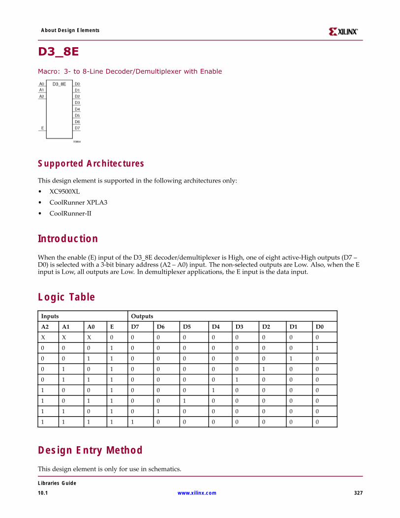
About Design Elements
D3_8E
Macro: 3- to 8-Line Decoder/Demultiplexer with Enable
Supported Architectures
This design element is supported in the following architectures only:
• XC9500XL
• CoolRunner XPLA3
• CoolRunner-II
IntroductionWhen the enable (E) input of the D3_8E decoder/demultiplexer is High, one of eight active-High outputs (D7 –D0) is selected with a 3-bit binary address (A2 – A0) input. The non-selected outputs are Low. Also, when the Einput is Low, all outputs are Low. In demultiplexer applications, the E input is the data input.
Logic TableInputs Outputs
A2 A1 A0 E D7 D6 D5 D4 D3 D2 D1 D0
X X X 0 0 0 0 0 0 0 0 0
0 0 0 1 0 0 0 0 0 0 0 1
0 0 1 1 0 0 0 0 0 0 1 0
0 1 0 1 0 0 0 0 0 1 0 0
0 1 1 1 0 0 0 0 1 0 0 0
1 0 0 1 0 0 0 1 0 0 0 0
1 0 1 1 0 0 1 0 0 0 0 0
1 1 0 1 0 1 0 0 0 0 0 0
1 1 1 1 1 0 0 0 0 0 0 0
Design Entry MethodThis design element is only for use in schematics.
Libraries Guide
10.1 www.xilinx.com 327

About Design Elements
For More Information• See the appropriate CPLD User Guide.
• See the appropriate CPLD Data Sheets.
Libraries Guide
328 www.xilinx.com 10.1

About Design Elements
D4_16E
Macro: 4- to 16-Line Decoder/Demultiplexer with Enable
Supported Architectures
This design element is supported in the following architectures only:
• XC9500XL
• CoolRunner XPLA3
• CoolRunner-II
IntroductionThis design element is a decoder/demultiplexer. When the enable (E) input of this design element is High, oneof 16 active-High outputs (D15 – D0) is selected with a 4-bit binary address (A3 – A0) input. The non-selectedoutputs are Low. Also, when the E input is Low, all outputs are Low. In demultiplexer applications, the Einput is the data input.
Design Entry MethodThis design element is only for use in schematics.
For More Information• See the appropriate CPLD User Guide.
• See the appropriate CPLD Data Sheets.
Libraries Guide
10.1 www.xilinx.com 329

About Design Elements
FD
Macro: D Flip-Flop
Supported ArchitecturesThis design element is supported in the following architectures only:• XC9500XL• CoolRunner XPLA3• CoolRunner-II
IntroductionThis design element is a D-type flip-flop with data input (D) and data output (Q). The data on the D inputs isloaded into the flip-flop during the Low-to-High clock (C) transition.
This flip-flop is asynchronously cleared, outputs Low, when power is applied. For CPLD devices, you cansimulate power-on by applying a High-level pulse on the PRLD global net.
Logic TableInputs Outputs
D C Q
0 ↑ 0
1 ↑ 1
Design Entry MethodThis design element is only for use in schematics.
Available AttributesAttribute Type Allowed Values Default Description
INIT Binary 0, 1 0 Sets the initial value of Q output after configuration
For More Information• See the appropriate CPLD User Guide.• See the appropriate CPLD Data Sheets.
Libraries Guide
330 www.xilinx.com 10.1

About Design Elements
FD16
Macro: Multiple D Flip-Flop
Supported Architectures
This design element is supported in the following architectures only:
• XC9500XL
• CoolRunner XPLA3
• CoolRunner-II
IntroductionThis design element is a multiple D-type flip-flops with data inputs (D) and data outputs (Q), with a 16-bitregister, each with a common clock (C). The data on the D inputs is loaded into the flip-flop during theLow-to-High clock (C) transition.
This flip-flop is asynchronously cleared, outputs Low, when power is applied. For CPLD devices, you cansimulate power-on by applying a High-level pulse on the PRLD global net.
Logic TableInputs Outputs
Dz – D0 C Qz – Q0
0 ↑ 0
1 ↑ 1
z = bit-width - 1
Design Entry MethodThis design element is only for use in schematics.
For More Information• See the appropriate CPLD User Guide.
• See the appropriate CPLD Data Sheets.
Libraries Guide
10.1 www.xilinx.com 331

About Design Elements
FD16CE
Macro: 16-Bit Data Register with Clock Enable and Asynchronous Clear
Supported ArchitecturesThis design element is supported in the following architectures only:• XC9500XL• CoolRunner XPLA3• CoolRunner-II
IntroductionThis design element is a 16-bit data register with clock enable and asynchronous clear. When clock enable (CE) isHigh and asynchronous clear (CLR) is Low, the data on the data inputs (D) is transferred to the correspondingdata outputs (Q) during the Low-to-High clock (C) transition. When CLR is High, it overrides all other inputsand resets the data outputs (Q) Low. When CE is Low, clock transitions are ignored.
This register is asynchronously cleared, outputs Low, when power is applied. For CPLD devices, you cansimulate power-on by applying a High-level pulse on the PRLD global net.
Logic TableInputs Outputs
CLR CE Dz – D0 C Qz – Q0
1 X X X 0
0 0 X X No Change
0 1 Dn ↑ Dn
z = bit-width - 1
Design Entry MethodThis design element is only for use in schematics.
Available AttributesAttribute Type Allowed Values Default Description
INIT Binary Any 16-bitValue
All zeros Sets the initial value of Q output after configuration
Libraries Guide
332 www.xilinx.com 10.1

About Design Elements
For More Information• See the appropriate CPLD User Guide.
• See the appropriate CPLD Data Sheets.
Libraries Guide
10.1 www.xilinx.com 333

About Design Elements
FD16RE
Macro: 16-Bit Data Register with Clock Enable and Synchronous Reset
Supported ArchitecturesThis design element is supported in the following architectures only:• XC9500XL• CoolRunner XPLA3• CoolRunner-II
IntroductionThis design element is a 16-bit data registers. When the clock enable (CE) input is High, and the synchronousreset (R) input is Low, the data on the data inputs (D) is transferred to the corresponding data outputs (Q0)during the Low-to-High clock (C) transition. When R is High, it overrides all other inputs and resets the dataoutputs (Q) Low on the Low-to-High clock transition. When CE is Low, clock transitions are ignored.
This register is asynchronously cleared, outputs Low, when power is applied. For CPLD devices, you cansimulate power-on by applying a High-level pulse on the PRLD global net.
Logic TableInputs Outputs
R CE Dz – D0 C Qz – Q0
1 X X ↑ 0
0 0 X X No Change
0 1 Dn ↑ Dn
z = bit-width - 1
Design Entry MethodThis design element is only for use in schematics.
Available AttributesAttribute Type Allowed Values Default Description
INIT Binary Any 16-Bit Value All zeros Sets the initial value of Q output afterconfiguration.
Libraries Guide
334 www.xilinx.com 10.1

About Design Elements
For More Information• See the appropriate CPLD User Guide.
• See the appropriate CPLD Data Sheets.
Libraries Guide
10.1 www.xilinx.com 335
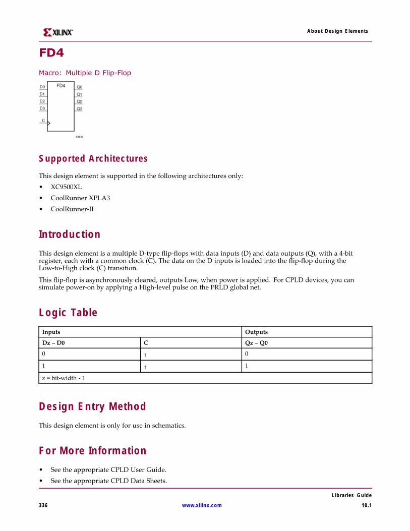
About Design Elements
FD4
Macro: Multiple D Flip-Flop
Supported Architectures
This design element is supported in the following architectures only:• XC9500XL• CoolRunner XPLA3• CoolRunner-II
IntroductionThis design element is a multiple D-type flip-flops with data inputs (D) and data outputs (Q), with a 4-bitregister, each with a common clock (C). The data on the D inputs is loaded into the flip-flop during theLow-to-High clock (C) transition.
This flip-flop is asynchronously cleared, outputs Low, when power is applied. For CPLD devices, you cansimulate power-on by applying a High-level pulse on the PRLD global net.
Logic TableInputs Outputs
Dz – D0 C Qz – Q0
0 ↑ 0
1 ↑ 1
z = bit-width - 1
Design Entry MethodThis design element is only for use in schematics.
For More Information• See the appropriate CPLD User Guide.• See the appropriate CPLD Data Sheets.
Libraries Guide
336 www.xilinx.com 10.1

About Design Elements
FD4CEMacro: 4-Bit Data Register with Clock Enable and Asynchronous Clear
Supported ArchitecturesThis design element is supported in the following architectures only:• XC9500XL• CoolRunner XPLA3• CoolRunner-II
IntroductionThis design element is a 4-bit data register with clock enable and asynchronous clear. When clock enable (CE) isHigh and asynchronous clear (CLR) is Low, the data on the data inputs (D) is transferred to the correspondingdata outputs (Q) during the Low-to-High clock (C) transition. When CLR is High, it overrides all other inputsand resets the data outputs (Q) Low. When CE is Low, clock transitions are ignored.
This register is asynchronously cleared, outputs Low, when power is applied. For CPLD devices, you cansimulate power-on by applying a High-level pulse on the PRLD global net.
Logic TableInputs Outputs
CLR CE Dz – D0 C Qz – Q0
1 X X X 0
0 0 X X No Change
0 1 Dn ↑ Dn
z = bit-width - 1
Design Entry MethodThis design element is only for use in schematics.
Available AttributesAttribute Type Allowed Values Default Description
INIT Binary Any 4-Bit Value All zeros Sets the initial value of Q output afterconfiguration.
Libraries Guide
10.1 www.xilinx.com 337

About Design Elements
For More Information• See the appropriate CPLD User Guide.
• See the appropriate CPLD Data Sheets.
Libraries Guide
338 www.xilinx.com 10.1
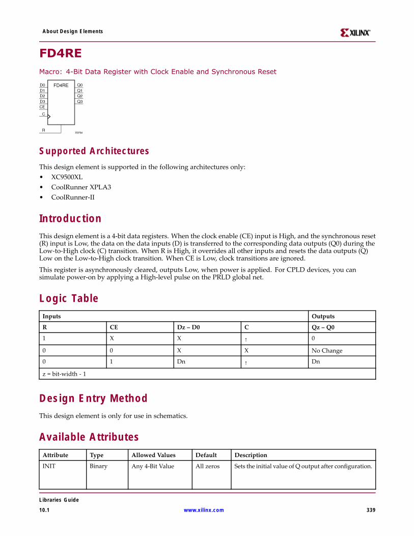
About Design Elements
FD4REMacro: 4-Bit Data Register with Clock Enable and Synchronous Reset
Supported ArchitecturesThis design element is supported in the following architectures only:• XC9500XL• CoolRunner XPLA3• CoolRunner-II
IntroductionThis design element is a 4-bit data registers. When the clock enable (CE) input is High, and the synchronous reset(R) input is Low, the data on the data inputs (D) is transferred to the corresponding data outputs (Q0) during theLow-to-High clock (C) transition. When R is High, it overrides all other inputs and resets the data outputs (Q)Low on the Low-to-High clock transition. When CE is Low, clock transitions are ignored.
This register is asynchronously cleared, outputs Low, when power is applied. For CPLD devices, you cansimulate power-on by applying a High-level pulse on the PRLD global net.
Logic TableInputs Outputs
R CE Dz – D0 C Qz – Q0
1 X X ↑ 0
0 0 X X No Change
0 1 Dn ↑ Dn
z = bit-width - 1
Design Entry MethodThis design element is only for use in schematics.
Available AttributesAttribute Type Allowed Values Default Description
INIT Binary Any 4-Bit Value All zeros Sets the initial value of Q output after configuration.
Libraries Guide
10.1 www.xilinx.com 339

About Design Elements
For More Information• See the appropriate CPLD User Guide.
• See the appropriate CPLD Data Sheets.
Libraries Guide
340 www.xilinx.com 10.1

About Design Elements
FD8
Macro: Multiple D Flip-Flop
Supported Architectures
This design element is supported in the following architectures only:
• XC9500XL
• CoolRunner XPLA3
• CoolRunner-II
IntroductionThis design element is a multiple D-type flip-flops with data inputs (D) and data outputs (Q), with a 8-bitregister, each with a common clock (C). The data on the D inputs is loaded into the flip-flop during theLow-to-High clock (C) transition.
This flip-flop is asynchronously cleared, outputs Low, when power is applied. For CPLD devices, you cansimulate power-on by applying a High-level pulse on the PRLD global net.
Logic TableInputs Outputs
Dz – D0 C Qz – Q0
0 ↑ 0
1 ↑ 1
z = bit-width - 1
Design Entry MethodThis design element is only for use in schematics.
For More Information• See the appropriate CPLD User Guide.
• See the appropriate CPLD Data Sheets.
Libraries Guide
10.1 www.xilinx.com 341
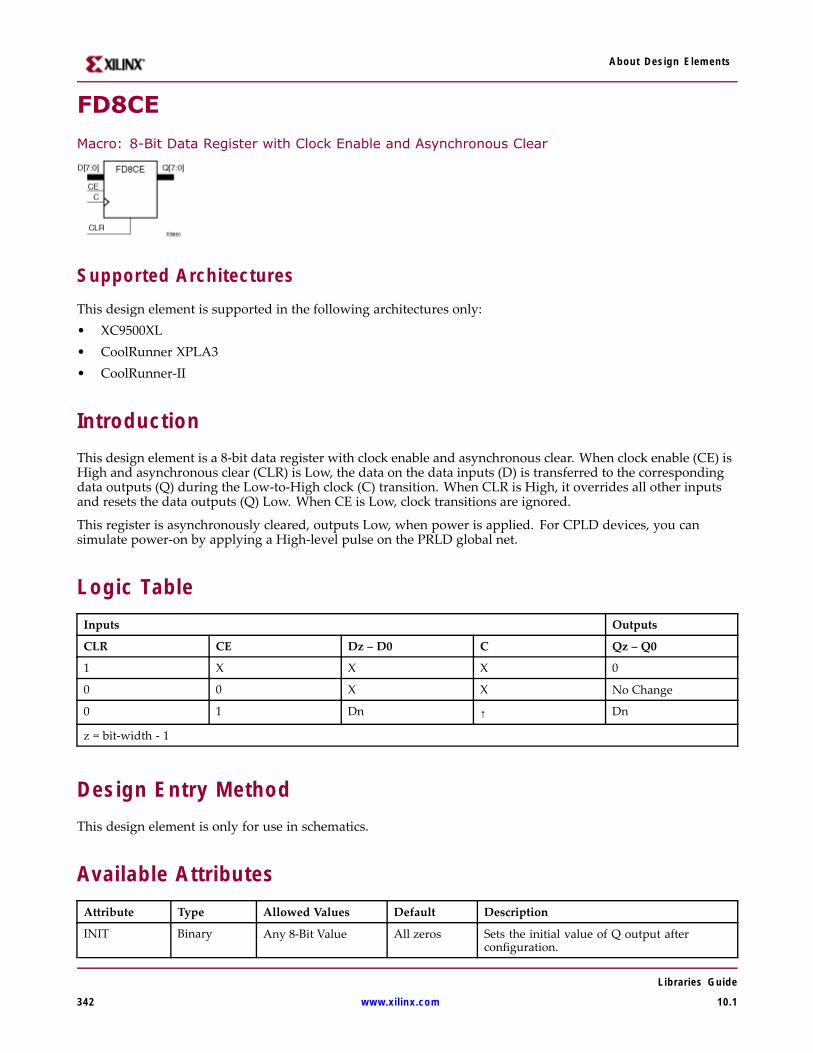
About Design Elements
FD8CE
Macro: 8-Bit Data Register with Clock Enable and Asynchronous Clear
Supported ArchitecturesThis design element is supported in the following architectures only:• XC9500XL• CoolRunner XPLA3• CoolRunner-II
IntroductionThis design element is a 8-bit data register with clock enable and asynchronous clear. When clock enable (CE) isHigh and asynchronous clear (CLR) is Low, the data on the data inputs (D) is transferred to the correspondingdata outputs (Q) during the Low-to-High clock (C) transition. When CLR is High, it overrides all other inputsand resets the data outputs (Q) Low. When CE is Low, clock transitions are ignored.
This register is asynchronously cleared, outputs Low, when power is applied. For CPLD devices, you cansimulate power-on by applying a High-level pulse on the PRLD global net.
Logic TableInputs Outputs
CLR CE Dz – D0 C Qz – Q0
1 X X X 0
0 0 X X No Change
0 1 Dn ↑ Dn
z = bit-width - 1
Design Entry MethodThis design element is only for use in schematics.
Available AttributesAttribute Type Allowed Values Default Description
INIT Binary Any 8-Bit Value All zeros Sets the initial value of Q output afterconfiguration.
Libraries Guide
342 www.xilinx.com 10.1

About Design Elements
For More Information• See the appropriate CPLD User Guide.
• See the appropriate CPLD Data Sheets.
Libraries Guide
10.1 www.xilinx.com 343

About Design Elements
FD8RE
Macro: 8-Bit Data Register with Clock Enable and Synchronous Reset
Supported ArchitecturesThis design element is supported in the following architectures only:• XC9500XL• CoolRunner XPLA3• CoolRunner-II
IntroductionThis design element is an 8-bit data register. When the clock enable (CE) input is High, and the synchronous reset(R) input is Low, the data on the data inputs (D) is transferred to the corresponding data outputs (Q0) during theLow-to-High clock (C) transition. When R is High, it overrides all other inputs and resets the data outputs (Q)Low on the Low-to-High clock transition. When CE is Low, clock transitions are ignored.
This register is asynchronously cleared, outputs Low, when power is applied. For CPLD devices, you cansimulate power-on by applying a High-level pulse on the PRLD global net.
Logic TableInputs Outputs
R CE Dz – D0 C Qz – Q0
1 X X ↑ 0
0 0 X X No Change
0 1 Dn ↑ Dn
z = bit-width - 1
Design Entry MethodThis design element is only for use in schematics.
Available AttributesAttribute Type Allowed Values Default Description
INIT Binary Any 8-Bit Value Allzeros
Sets the initial value of Q output afterconfiguration.
Libraries Guide
344 www.xilinx.com 10.1

About Design Elements
For More Information• See the appropriate CPLD User Guide.
• See the appropriate CPLD Data Sheets.
Libraries Guide
10.1 www.xilinx.com 345

About Design Elements
FDCMacro: D Flip-Flop with Asynchronous Clear
Supported ArchitecturesThis design element is supported in the following architectures only:• XC9500XL• CoolRunner XPLA3• CoolRunner-II
IntroductionThis design element is a single D-type flip-flop with data (D) and asynchronous clear (CLR) inputs and dataoutput (Q). The asynchronous CLR, when High, overrides all other inputs and sets the (Q) output Low. The dataon the (D) input is loaded into the flip-flop when CLR is Low on the Low-to-High clock transition.
This flip-flop is asynchronously cleared, outputs Low, when power is applied. For CPLD devices, you cansimulate power-on by applying a High-level pulse on the PRLD global net.
Logic TableInputs Outputs
CLR D C Q
1 X X 0
0 D ↑ D
Design Entry MethodThis design element is only for use in schematics.
Available AttributesAttribute Type Allowed Values Default Description
INIT Binary 0, 1 0 Sets the initial value of Q output after configuration
For More Information• See the appropriate CPLD User Guide.• See the appropriate CPLD Data Sheets.
Libraries Guide
346 www.xilinx.com 10.1

About Design Elements
FDCEPrimitive: D Flip-Flop with Clock Enable and Asynchronous Clear
Supported ArchitecturesThis design element is supported in the following architectures only:• XC9500XL• CoolRunner XPLA3• CoolRunner-II
IntroductionThis design element is a single D-type flip-flop with clock enable and asynchronous clear. When clock enable(CE) is High and asynchronous clear (CLR) is Low, the data on the data input (D) of this design element istransferred to the corresponding data output (Q) during the Low-to-High clock (C) transition. When CLR is High,it overrides all other inputs and resets the data output (Q) Low. When CE is Low, clock transitions are ignored.
For XC9500XL and XC9500XV devices, logic connected to the clock enable (CE) input may be implemented usingthe clock enable product term (p-term) in the macrocell, provided the logic can be completely implemented usingthe single p-term available for clock enable without requiring feedback from another macrocell. Only FDCE andFDPE flip-flops may take advantage of the clock-enable p-term.
This flip-flop is asynchronously cleared, outputs Low, when power is applied. For CPLD devices, you cansimulate power-on by applying a High-level pulse on the PRLD global net.
Logic TableInputs Outputs
CLR CE D C Q
1 X X X 0
0 0 X X No Change
0 1 D ↑ D
Design Entry MethodInstantiation Yes
Inference Recommended
Coregen and wizards No
Macro support No
This design element can be used in schematics.
Libraries Guide
10.1 www.xilinx.com 347
About Design Elements
Available AttributesAttribute Type Allowed Values Default Description
INIT Binary 0,1 0 Sets the initial value of Q output after configuration.
VHDL Instantiation Template
Unless they already exist, copy the following two statements and paste them before the entity declaration.Library UNISIM;use UNISIM.vcomponents.all;
-- FDCE: Single Data Rate D Flip-Flop with Asynchronous Clear and-- Clock Enable (posedge clk). All families.-- Xilinx HDL Libraries Guide, version 10.1.2
FDCE_inst : FDCEgeneric map (INIT => ’0’) -- Initial value of register (’0’ or ’1’)port map (Q => Q, -- Data outputC => C, -- Clock inputCE => CE, -- Clock enable inputCLR => CLR, -- Asynchronous clear inputD => D -- Data input);
-- End of FDCE_inst instantiation
Verilog Instantiation Template// FDCE: Single Data Rate D Flip-Flop with Asynchronous Clear and// Clock Enable (posedge clk).// All families.// Xilinx HDL Libraries Guide, version 10.1.2
FDCE #(.INIT(1’b0) // Initial value of register (1’b0 or 1’b1)) FDCE_inst (.Q(Q), // Data output.C(C), // Clock input.CE(CE), // Clock enable input.CLR(CLR), // Asynchronous clear input.D(D) // Data input);
// End of FDCE_inst instantiation
For More Information• See the appropriate CPLD User Guide.
• See the appropriate CPLD Data Sheets.
Libraries Guide
348 www.xilinx.com 10.1

About Design Elements
FDCP
Primitive: D Flip-Flop with Asynchronous Preset and Clear
Supported Architectures
This design element is supported in the following architectures only:
• XC9500XL
• CoolRunner XPLA3
• CoolRunner-II
IntroductionThis design element is a single D-type flip-flop with data (D), asynchronous preset (PRE) and clear (CLR)inputs, and data output (Q). The asynchronous PRE, when High, sets the (Q) output High; CLR, when High,resets the output Low. Data on the (D) input is loaded into the flip-flop when PRE and CLR are Low on theLow-to-High clock (C) transition.
This flip-flop is asynchronously cleared, outputs Low, when power is applied. For CPLD devices, you cansimulate power-on by applying a High-level pulse on the PRLD global net.
Logic TableInputs Outputs
CLR PRE D C Q
1 X X X 0
0 1 X X 1
0 0 D ↑ D
Design Entry MethodThis design element is only for use in schematics.
Libraries Guide
10.1 www.xilinx.com 349

About Design Elements
Available AttributesAttribute Type Allowed Values Default Description
INIT Binary 0 or 1 0 Sets the initial value of Q output afterconfiguration.
For More Information• See the appropriate CPLD User Guide.
• See the appropriate CPLD Data Sheets.
Libraries Guide
350 www.xilinx.com 10.1

About Design Elements
FDCPE
Primitive: D Flip-Flop with Clock Enable and Asynchronous Preset and Clear
Supported ArchitecturesThis design element is supported in the following architectures only:• XC9500XL• CoolRunner XPLA3• CoolRunner-II
IntroductionThis design element is a single D-type flip-flop with data (D), clock enable (CE), asynchronous preset (PRE),and asynchronous clear (CLR) inputs. The asynchronous active high PRE sets the Q output High; that activehigh CLR resets the output Low and has precedence over the PRE input. Data on the D input is loaded into theflip-flop when PRE and CLR are Low and CE is High on the Low-to-High clock (C) transition. When CE is Low,the clock transitions are ignored and the previous value is retained. The FDCPE is generally implemented as aslice or IOB register within the device.
For CPLD devices, you can simulate power-on by applying a High-level pulse on the PRLD global net. For FPGAdevices, upon power-up, the initial value of this component is specified by the INIT attribute. If a subsequentGSR (Global Set/Reset) is asserted, the flop is asynchronously set to the INIT value.
Note While this device supports the use of asynchronous set and reset, it is not generally recommended tobe used for in most cases. Use of asynchronous signals pose timing issues within the design that are difficultto detect and control and also have an adverse affect on logic optimization causing a larger design that canconsume more power than if a synchronous set or reset is used.
Logic TableInputs Outputs
CLR PRE CE D C Q
1 X X X X 0
0 1 X X X 1
0 0 0 X X No Change
0 0 1 D ↑ D
Libraries Guide
10.1 www.xilinx.com 351

About Design Elements
Port DescriptionsPort Direction Width Function
Q Output 1 Data output
C Input 1 Clock input
CE Input 1 Clock enable input
CLR Input 1 Asynchronous clear input
D Input 1 Data input
PRE Input 1 Asynchronous set input
Design Entry MethodInstantiation Yes
Inference Recommended
Coregen and wizards No
Macro support No
This design element can be used in schematics.
Available AttributesAttribute Type Allowed Values Default Description
INIT Binary 0,1 0 Sets the initial value of Q output afterconfiguration and on GSR.
VHDL Instantiation Template
Unless they already exist, copy the following two statements and paste them before the entity declaration.Library UNISIM;use UNISIM.vcomponents.all;
-- FDCPE: Single Data Rate D Flip-Flop with Asynchronous Clear, Set and-- Clock Enable (posedge clk). All families.-- Xilinx HDL Libraries Guide, version 10.1.2
FDCPE_inst : FDCPEgeneric map (INIT => ’0’) -- Initial value of register (’0’ or ’1’)port map (Q => Q, -- Data outputC => C, -- Clock inputCE => CE, -- Clock enable inputCLR => CLR, -- Asynchronous clear inputD => D, -- Data inputPRE => PRE -- Asynchronous set input);
-- End of FDCPE_inst instantiation
Libraries Guide
352 www.xilinx.com 10.1

About Design Elements
Verilog Instantiation Template// FDCPE: Single Data Rate D Flip-Flop with Asynchronous Clear, Set and// Clock Enable (posedge clk).// All families.// Xilinx HDL Libraries Guide, version 10.1.2
FDCPE #(.INIT(1’b0) // Initial value of register (1’b0 or 1’b1)) FDCPE_inst (.Q(Q), // Data output.C(C), // Clock input.CE(CE), // Clock enable input.CLR(CLR), // Asynchronous clear input.D(D), // Data input.PRE(PRE) // Asynchronous set input);
// End of FDCPE_inst instantiation
For More Information• See the appropriate CPLD User Guide.
• See the appropriate CPLD Data Sheets.
Libraries Guide
10.1 www.xilinx.com 353

About Design Elements
FDD
Macro: Dual Edge Triggered D Flip-Flop
Supported Architectures
This design element is supported in the following architectures only:
CoolRunner-II
IntroductionThis design element is a single dual edge triggered D-type flip-flop with data input (D) and data output (Q). Thedata on the D input is loaded into the flip-flop during the Low-to-High and the High-to-Low clock (C) transitions.
This flip-flop is asynchronously cleared, outputs Low, when power is applied. For CPLD devices, you cansimulate power-on by applying a High-level pulse on the PRLD global net.
Logic TableInputs Outputs
D C Q
0 ↑ 0
1 ↑ 1
0 ↓ 0
1 ↓ 1
Design Entry MethodThis design element is only for use in schematics.
For More Information• See the appropriate CPLD User Guide.
• See the appropriate CPLD Data Sheets.
Libraries Guide
354 www.xilinx.com 10.1
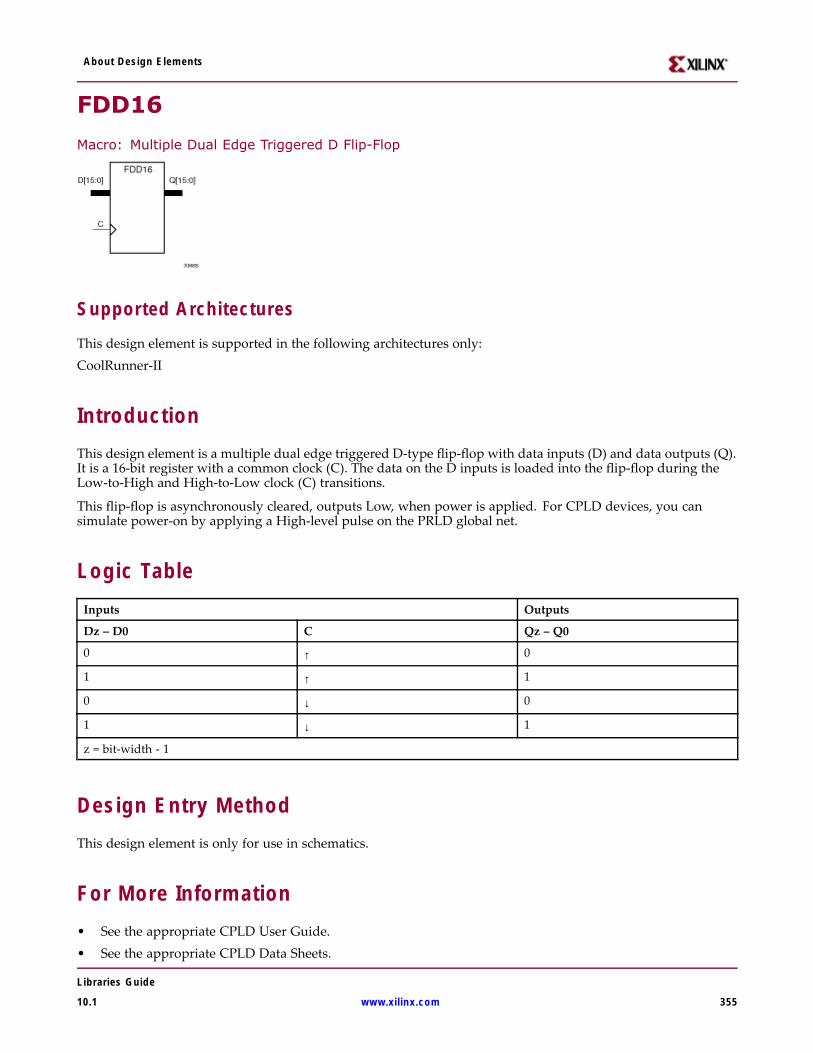
About Design Elements
FDD16
Macro: Multiple Dual Edge Triggered D Flip-Flop
Supported Architectures
This design element is supported in the following architectures only:CoolRunner-II
IntroductionThis design element is a multiple dual edge triggered D-type flip-flop with data inputs (D) and data outputs (Q).It is a 16-bit register with a common clock (C). The data on the D inputs is loaded into the flip-flop during theLow-to-High and High-to-Low clock (C) transitions.
This flip-flop is asynchronously cleared, outputs Low, when power is applied. For CPLD devices, you cansimulate power-on by applying a High-level pulse on the PRLD global net.
Logic TableInputs Outputs
Dz – D0 C Qz – Q0
0 ↑ 0
1 ↑ 1
0 ↓ 0
1 ↓ 1
z = bit-width - 1
Design Entry MethodThis design element is only for use in schematics.
For More Information• See the appropriate CPLD User Guide.• See the appropriate CPLD Data Sheets.
Libraries Guide
10.1 www.xilinx.com 355

About Design Elements
FDD16CE
Macro: 16-Bit Dual Edge Triggered Data Register with Clock Enable and Asynchronous Clear
Supported ArchitecturesThis design element is supported in the following architectures only:CoolRunner-II
IntroductionThis design element is a 16-bit data registers with clock enable and asynchronous clear. When clock enable (CE)is High and asynchronous clear (CLR) is Low, the data on the data inputs (D) is transferred to the correspondingdata outputs (Q) during the Low-to-High and High-to-Low clock (C) transitions. When CLR is High, it overridesall other inputs and resets the data outputs (Q) Low. When CE is Low, clock transitions are ignored.
This register is asynchronously cleared, outputs Low, when power is applied. For CPLD devices, you cansimulate power-on by applying a High-level pulse on the PRLD global net.
Logic TableInputs Outputs
CLR CE Dz – D0 C Qz – Q0
1 X X X 0
0 0 X X No Change
0 1 Dn ↑ Dn
0 1 Dn ↓ Dn
z = bit-width - 1
Design Entry MethodThis design element is only for use in schematics.
For More Information• See the appropriate CPLD User Guide.• See the appropriate CPLD Data Sheets.
Libraries Guide
356 www.xilinx.com 10.1

About Design Elements
FDD16REMacro: 16-Bit Dual Edge Triggered Data Register with Clock Enable and Synchronous Reset
Supported ArchitecturesThis design element is supported in the following architectures only:CoolRunner-II
IntroductionThis design element is a 16-bit data register. When the clock enable (CE) input is High, and the synchronousreset (R) input is Low, the data on the data inputs (D) is transferred to the corresponding data outputs (Q0)during the Low-to-High or High-to-Low clock (C) transition. When R is High, it overrides all other inputs andresets the data outputs (Q) Low on the Low-to-High and High-to-Low clock transitions. When CE is Low,clock transitions are ignored.
This register is asynchronously cleared, outputs Low, when power is applied. For CPLD devices, you cansimulate power-on by applying a High-level pulse on the PRLD global net.
Logic TableInputs Outputs
R CE Dz – D0 C Qz – Q0
1 X X ↑ 0
1 X X ↓ 0
0 0 X X No Change
0 1 Dn ↑ Dn
0 1 Dn ↓ Dn
z = bit-width - 1
Design Entry MethodThis design element is only for use in schematics.
For More Information• See the appropriate CPLD User Guide.• See the appropriate CPLD Data Sheets.
Libraries Guide
10.1 www.xilinx.com 357

About Design Elements
FDD4Macro: Multiple Dual Edge Triggered D Flip-Flop
Supported ArchitecturesThis design element is supported in the following architectures only:CoolRunner-II
IntroductionThis design element is a multiple dual edge triggered D-type flip-flop with data inputs (D) and data outputs (Q).It is a 4-bit register with a common clock (C). The data on the D inputs is loaded into the flip-flop during theLow-to-High and High-to-Low clock (C) transitions.
This flip-flop is asynchronously cleared, outputs Low, when power is applied. For CPLD devices, you cansimulate power-on by applying a High-level pulse on the PRLD global net.
Logic TableInputs Outputs
Dz – D0 C Qz – Q0
0 ↑ 0
1 ↑ 1
0 ↓ 0
1 ↓ 1
z = bit-width - 1
Design Entry MethodThis design element is only for use in schematics.
For More Information• See the appropriate CPLD User Guide.• See the appropriate CPLD Data Sheets.
Libraries Guide
358 www.xilinx.com 10.1

About Design Elements
FDD4CEMacro: 4-Bit Dual Edge Triggered Data Register with Clock Enable and Asynchronous Clear
Supported ArchitecturesThis design element is supported in the following architectures only:CoolRunner-II
IntroductionThis design element is a 4-bit data registers with clock enable and asynchronous clear. When clock enable (CE) isHigh and asynchronous clear (CLR) is Low, the data on the data inputs (D) is transferred to the correspondingdata outputs (Q) during the Low-to-High and High-to-Low clock (C) transitions. When CLR is High, it overridesall other inputs and resets the data outputs (Q) Low. When CE is Low, clock transitions are ignored.
This register is asynchronously cleared, outputs Low, when power is applied. For CPLD devices, you cansimulate power-on by applying a High-level pulse on the PRLD global net.
Logic TableInputs Outputs
CLR CE Dz – D0 C Qz – Q0
1 X X X 0
0 0 X X No Change
0 1 Dn ↑ Dn
0 1 Dn ↓ Dn
z = bit-width - 1
Design Entry MethodThis design element is only for use in schematics.
For More Information• See the appropriate CPLD User Guide.
Libraries Guide
10.1 www.xilinx.com 359

About Design Elements
• See the appropriate CPLD Data Sheets.
Libraries Guide
360 www.xilinx.com 10.1

About Design Elements
FDD4RE
Macro: 4-Bit Dual Edge Triggered Data Register with Clock Enable and Synchronous Reset
Supported Architectures
This design element is supported in the following architectures only:CoolRunner-II
IntroductionThis design element is a 4-bit data register. When the clock enable (CE) input is High, and the synchronous reset(R) input is Low, the data on the data inputs (D) is transferred to the corresponding data outputs (Q0) duringthe Low-to-High or High-to-Low clock (C) transition. When R is High, it overrides all other inputs and resetsthe data outputs (Q) Low on the Low-to-High and High-to-Low clock transitions. When CE is Low, clocktransitions are ignored.
This register is asynchronously cleared, outputs Low, when power is applied. For CPLD devices, you cansimulate power-on by applying a High-level pulse on the PRLD global net.
Logic TableInputs Outputs
R CE Dz – D0 C Qz – Q0
1 X X ↑ 0
1 X X ↓ 0
0 0 X X No Change
0 1 Dn ↑ Dn
0 1 Dn ↓ Dn
z = bit-width - 1
Design Entry MethodThis design element is only for use in schematics.
Libraries Guide
10.1 www.xilinx.com 361
About Design Elements
For More Information• See the appropriate CPLD User Guide.
• See the appropriate CPLD Data Sheets.
Libraries Guide
362 www.xilinx.com 10.1

About Design Elements
FDD8
Macro: Multiple Dual Edge Triggered D Flip-Flop
Supported Architectures
This design element is supported in the following architectures only:CoolRunner-II
IntroductionThis design element is a multiple dual edge triggered D-type flip-flop with data inputs (D) and data outputs (Q).It is an 8-bit register with a common clock (C). The data on the D inputs is loaded into the flip-flop during theLow-to-High and High-to-Low clock (C) transitions.
This flip-flop is asynchronously cleared, outputs Low, when power is applied. For CPLD devices, you cansimulate power-on by applying a High-level pulse on the PRLD global net.
Logic TableInputs Outputs
Dz – D0 C Qz – Q0
0 ↑ 0
1 ↑ 1
0 ↓ 0
1 ↓ 1
z = bit-width - 1
Design Entry MethodThis design element is only for use in schematics.
For More Information• See the appropriate CPLD User Guide.• See the appropriate CPLD Data Sheets.
Libraries Guide
10.1 www.xilinx.com 363

About Design Elements
FDD8CE
Macro: 8-Bit Dual Edge Triggered Data Register with Clock Enable and Asynchronous Clear
Supported ArchitecturesThis design element is supported in the following architectures only:CoolRunner-II
IntroductionThis design element is a 8-bit data registers with clock enable and asynchronous clear. When clock enable (CE) isHigh and asynchronous clear (CLR) is Low, the data on the data inputs (D) is transferred to the correspondingdata outputs (Q) during the Low-to-High and High-to-Low clock (C) transitions. When CLR is High, it overridesall other inputs and resets the data outputs (Q) Low. When CE is Low, clock transitions are ignored.
This register is asynchronously cleared, outputs Low, when power is applied. For CPLD devices, you cansimulate power-on by applying a High-level pulse on the PRLD global net.
Logic TableInputs Outputs
CLR CE Dz – D0 C Qz – Q0
1 X X X 0
0 0 X X No Change
0 1 Dn ↑ Dn
0 1 Dn ↓ Dn
z = bit-width - 1
Design Entry MethodThis design element is only for use in schematics.
For More Information• See the appropriate CPLD User Guide.• See the appropriate CPLD Data Sheets.
Libraries Guide
364 www.xilinx.com 10.1

About Design Elements
FDD8REMacro: 8-Bit Dual Edge Triggered Data Register with Clock Enable and Synchronous Reset
Supported ArchitecturesThis design element is supported in the following architectures only:CoolRunner-II
IntroductionThis design element is a 8-bit data register. When the clock enable (CE) input is High, and the synchronous reset(R) input is Low, the data on the data inputs (D) is transferred to the corresponding data outputs (Q0) duringthe Low-to-High or High-to-Low clock (C) transition. When R is High, it overrides all other inputs and resetsthe data outputs (Q) Low on the Low-to-High and High-to-Low clock transitions. When CE is Low, clocktransitions are ignored.
This register is asynchronously cleared, outputs Low, when power is applied. For CPLD devices, you cansimulate power-on by applying a High-level pulse on the PRLD global net.
Logic TableInputs Outputs
R CE Dz – D0 C Qz – Q0
1 X X ↑ 0
1 X X ↓ 0
0 0 X X No Change
0 1 Dn ↑ Dn
0 1 Dn ↓ Dn
z = bit-width - 1
Design Entry MethodThis design element is only for use in schematics.
For More Information• See the appropriate CPLD User Guide.• See the appropriate CPLD Data Sheets.
Libraries Guide
10.1 www.xilinx.com 365

About Design Elements
FDDC
Macro: D Dual Edge Triggered Flip-Flop with Asynchronous Clear
Supported ArchitecturesThis design element is supported in the following architectures only:CoolRunner-II
IntroductionThis design element is a single dual edge triggered D-type flip-flop with data (D) and asynchronous clear(CLR) inputs and data output (Q). The asynchronous CLR, when High, overrides all other inputs and sets theQ output Low. The data on the D input is loaded into the flip-flop when CLR is Low on the Low-to-Highand High-to-Low clock (C) transitions.
This flip-flop is asynchronously cleared, outputs Low, when power is applied. For CPLD devices, you cansimulate power-on by applying a High-level pulse on the PRLD global net.
Logic TableInputs Outputs
CLR D C Q
1 X X 0
0 1 ↑ 1
0 1 ↓ 1
0 0 ↑ 0
0 0 ↓ 0
Design Entry MethodThis design element is only for use in schematics.
For More Information• See the appropriate CPLD User Guide.• See the appropriate CPLD Data Sheets.
Libraries Guide
366 www.xilinx.com 10.1
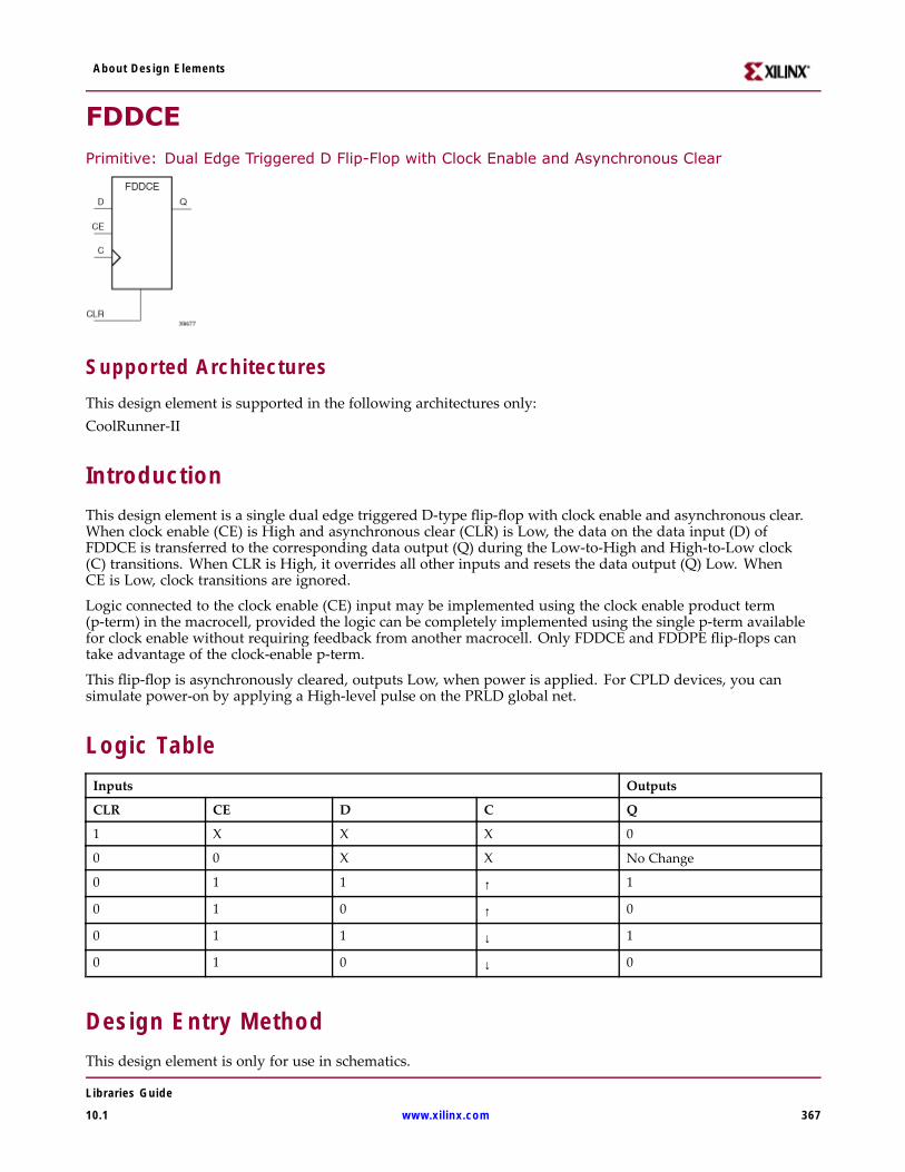
About Design Elements
FDDCEPrimitive: Dual Edge Triggered D Flip-Flop with Clock Enable and Asynchronous Clear
Supported ArchitecturesThis design element is supported in the following architectures only:CoolRunner-II
IntroductionThis design element is a single dual edge triggered D-type flip-flop with clock enable and asynchronous clear.When clock enable (CE) is High and asynchronous clear (CLR) is Low, the data on the data input (D) ofFDDCE is transferred to the corresponding data output (Q) during the Low-to-High and High-to-Low clock(C) transitions. When CLR is High, it overrides all other inputs and resets the data output (Q) Low. WhenCE is Low, clock transitions are ignored.
Logic connected to the clock enable (CE) input may be implemented using the clock enable product term(p-term) in the macrocell, provided the logic can be completely implemented using the single p-term availablefor clock enable without requiring feedback from another macrocell. Only FDDCE and FDDPE flip-flops cantake advantage of the clock-enable p-term.
This flip-flop is asynchronously cleared, outputs Low, when power is applied. For CPLD devices, you cansimulate power-on by applying a High-level pulse on the PRLD global net.
Logic TableInputs Outputs
CLR CE D C Q
1 X X X 0
0 0 X X No Change
0 1 1 ↑ 1
0 1 0 ↑ 0
0 1 1 ↓ 1
0 1 0 ↓ 0
Design Entry MethodThis design element is only for use in schematics.
Libraries Guide
10.1 www.xilinx.com 367

About Design Elements
For More Information• See the appropriate CPLD User Guide.
• See the appropriate CPLD Data Sheets.
Libraries Guide
368 www.xilinx.com 10.1

About Design Elements
FDDCP
Primitive: Dual Edge Triggered D Flip-Flop Asynchronous Preset and Clear
Supported Architectures
This design element is supported in the following architectures only:
CoolRunner-II
IntroductionThis design element is a single dual edge triggered D-type flip-flop with data (D), asynchronous preset (PRE)and clear (CLR) inputs, and data output (Q). The asynchronous PRE, when High, sets the Q output High; CLR,when High, resets the output Low. Data on the D input is loaded into the flip-flop when PRE and CLR are Lowon the Low-to-High and High-to-Low clock (C) transitions.
This flip-flop is asynchronously cleared, outputs Low, when power is applied. For CPLD devices, you cansimulate power-on by applying a High-level pulse on the PRLD global net.
Logic TableInputs Outputs
CLR PRE D C Q
1 X X X 0
0 1 X X 1
0 0 0 ↑ 0
0 0 1 ↑ 1
0 0 0 ↓ 0
0 0 1 ↓ 1
Design Entry MethodThis design element is only for use in schematics.
Libraries Guide
10.1 www.xilinx.com 369

About Design Elements
For More Information• See the appropriate CPLD User Guide.
• See the appropriate CPLD Data Sheets.
Libraries Guide
370 www.xilinx.com 10.1

About Design Elements
FDDCPEMacro: Dual Edge Triggered D Flip-Flop with Clock Enable and Asynchronous Preset and Clear
Supported ArchitecturesThis design element is supported in the following architectures only:CoolRunner-II
IntroductionThis design element is a single dual edge triggered D-type flip-flop with data (D), clock enable (CE),asynchronous preset (PRE), and asynchronous clear (CLR) inputs and data output (Q). The asynchronous PRE,when High, sets the Q output High; CLR, when High, resets the output Low. Data on the D input is loadedinto the flip-flop when PRE and CLR are Low and CE is High on the Low-to-High and High-to-Low clock (C)transitions. When CE is Low, the clock transitions are ignored.
This flip-flop is asynchronously cleared, outputs Low, when power is applied. For CPLD devices, you cansimulate power-on by applying a High-level pulse on the PRLD global net.
Logic TableInputs Outputs
CLR PRE CE D C Q
1 X X X X 0
0 1 X X X 1
0 0 0 X X No Change
0 0 1 0 ↑ 0
0 0 1 1 ↑ 1
0 0 1 0 ↓ 0
0 0 1 1 ↓ 1
Design Entry MethodThis design element is only for use in schematics.
Libraries Guide
10.1 www.xilinx.com 371

About Design Elements
For More Information• See the appropriate CPLD User Guide.
• See the appropriate CPLD Data Sheets.
Libraries Guide
372 www.xilinx.com 10.1

About Design Elements
FDDPMacro: Dual Edge Triggered D Flip-Flop with Asynchronous Preset
Supported ArchitecturesThis design element is supported in the following architectures only:CoolRunner-II
IntroductionThis design element is a single dual edge triggered D-type flip-flop with data (D) and asynchronous preset(PRE) inputs and data output (Q). The asynchronous PRE, when High, overrides all other inputs and presetsthe Q output High. The data on the D input is loaded into the flip-flop when PRE is Low on the Low-to-Highand High-to-Low clock (C) transitions.
This flip-flop is asynchronously cleared, outputs Low, when power is applied. For CPLD devices, you cansimulate power-on by applying a High-level pulse on the PRLD global net.
Logic TableInputs Outputs
PRE C D Q
1 X X 1
0 ↑ 1 1
0 ↑ 0 0
0 ↓ 1 1
0 ↓ 0 0
Design Entry MethodThis design element is only for use in schematics.
For More Information• See the appropriate CPLD User Guide.• See the appropriate CPLD Data Sheets.
Libraries Guide
10.1 www.xilinx.com 373

About Design Elements
FDDPE
Primitive: Dual Edge Triggered D Flip-Flop with Clock Enable and Asynchronous Preset
Supported Architectures
This design element is supported in the following architectures only:
CoolRunner-II
IntroductionThis design element is a single dual edge triggered D-type flip-flop with data (D), clock enable (CE), andasynchronous preset (PRE) inputs and data output (Q). The asynchronous PRE, when High, overrides all otherinputs and sets the Q output High. Data on the D input is loaded into the flip-flop when PRE is Low and CEis High on the Low-to-High and High-to-Low clock (C) transitions. When CE is Low, the clock transitionsare ignored.
Logic connected to the clock enable (CE) input may be implemented using the clock enable product term (p-term)in the macrocell, provided the logic can be completely implemented using the single p-term available for clockenable without requiring feedback from another macrocell. Only FDDCE and FDDPE flip-flops primitives maytake advantage of the clock-enable p-term.
This flip-flop is asynchronously cleared, outputs Low, when power is applied. For CPLD devices, you cansimulate power-on by applying a High-level pulse on the PRLD global net.
Logic TableInputs Outputs
PRE CE D C Q
1 X X X 1
0 0 X X No Change
0 1 0 ↑ 0
0 1 1 ↑ 1
0 1 0 ↓ 0
0 1 1 ↓ 1
Libraries Guide
374 www.xilinx.com 10.1

About Design Elements
Design Entry MethodThis design element is only for use in schematics.
For More Information• See the appropriate CPLD User Guide.
• See the appropriate CPLD Data Sheets.
Libraries Guide
10.1 www.xilinx.com 375
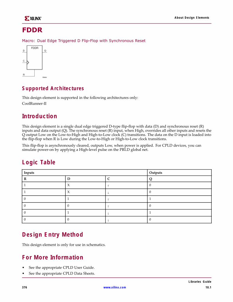
About Design Elements
FDDRMacro: Dual Edge Triggered D Flip-Flop with Synchronous Reset
Supported ArchitecturesThis design element is supported in the following architectures only:CoolRunner-II
IntroductionThis design element is a single dual edge triggered D-type flip-flop with data (D) and synchronous reset (R)inputs and data output (Q). The synchronous reset (R) input, when High, overrides all other inputs and resets theQ output Low on the Low-to-High and High-to-Low clock (C) transitions. The data on the D input is loaded intothe flip-flop when R is Low during the Low-to-High or High-to-Low clock transitions.
This flip-flop is asynchronously cleared, outputs Low, when power is applied. For CPLD devices, you cansimulate power-on by applying a High-level pulse on the PRLD global net.
Logic TableInputs Outputs
R D C Q
1 X ↑ 0
1 X ↓ 0
0 1 ↑ 1
0 0 ↑ 0
0 1 ↓ 1
0 0 ↓ 0
Design Entry MethodThis design element is only for use in schematics.
For More Information• See the appropriate CPLD User Guide.• See the appropriate CPLD Data Sheets.
Libraries Guide
376 www.xilinx.com 10.1
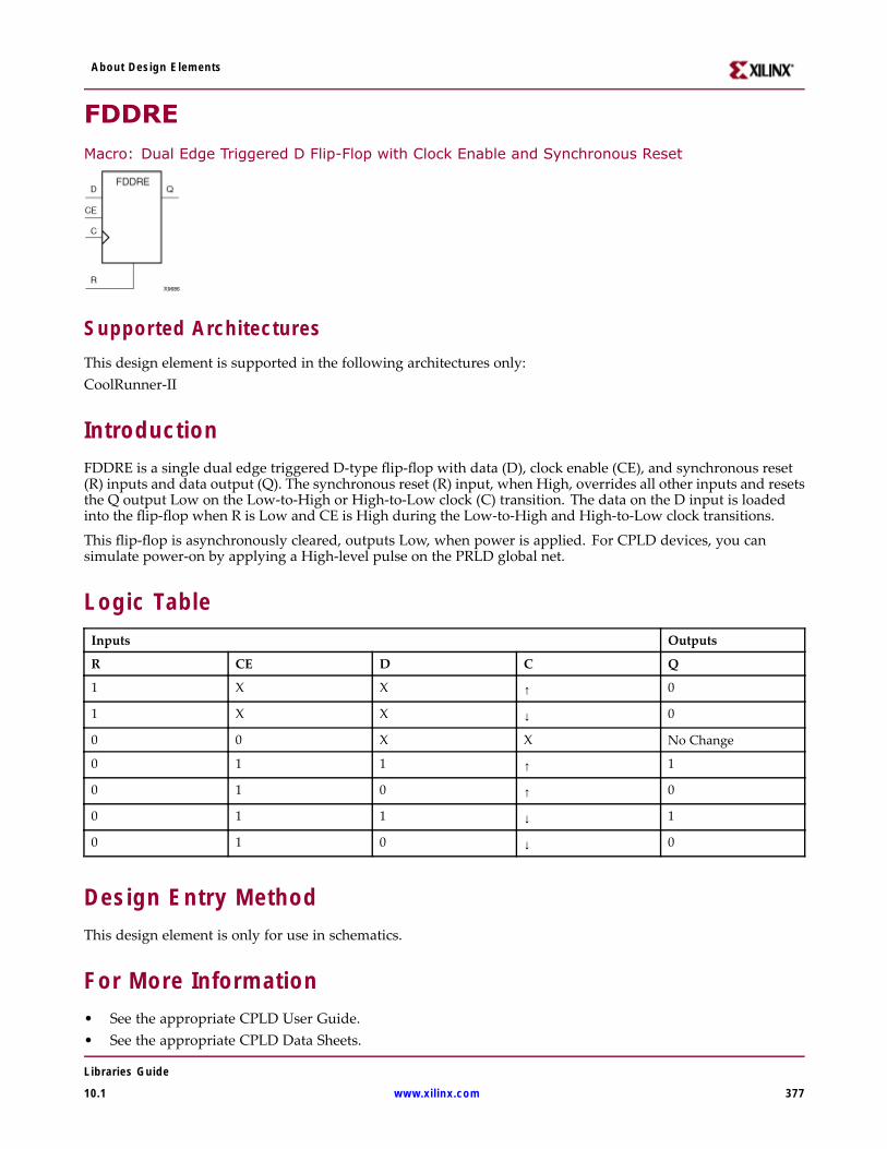
About Design Elements
FDDREMacro: Dual Edge Triggered D Flip-Flop with Clock Enable and Synchronous Reset
Supported ArchitecturesThis design element is supported in the following architectures only:CoolRunner-II
IntroductionFDDRE is a single dual edge triggered D-type flip-flop with data (D), clock enable (CE), and synchronous reset(R) inputs and data output (Q). The synchronous reset (R) input, when High, overrides all other inputs and resetsthe Q output Low on the Low-to-High or High-to-Low clock (C) transition. The data on the D input is loadedinto the flip-flop when R is Low and CE is High during the Low-to-High and High-to-Low clock transitions.
This flip-flop is asynchronously cleared, outputs Low, when power is applied. For CPLD devices, you cansimulate power-on by applying a High-level pulse on the PRLD global net.
Logic TableInputs Outputs
R CE D C Q
1 X X ↑ 0
1 X X ↓ 0
0 0 X X No Change
0 1 1 ↑ 1
0 1 0 ↑ 0
0 1 1 ↓ 1
0 1 0 ↓ 0
Design Entry MethodThis design element is only for use in schematics.
For More Information• See the appropriate CPLD User Guide.• See the appropriate CPLD Data Sheets.
Libraries Guide
10.1 www.xilinx.com 377

About Design Elements
FDDRSMacro: Dual Edge Triggered D Flip-Flop with Synchronous Reset and Set
Supported ArchitecturesThis design element is supported in the following architectures only:CoolRunner-II
IntroductionFDDRS is a single dual edge triggered D-type flip-flop with data (D), synchronous set (S), and synchronous reset(R) inputs and data output (Q). The synchronous reset (R) input, when High, overrides all other inputs and resetsthe Q output Low during the Low-to-High or High-to-Low clock (C) transitions. (Reset has precedence over Set.)When S is High and R is Low, the flip-flop is set, output High, during the Low-to-High or High-to-Low clocktransition. When R and S are Low, data on the (D) input is loaded into the flip-flop during the Low-to-High andHigh-to-Low clock transitions.
This flip-flop is asynchronously cleared, outputs Low, when power is applied. For CPLD devices, you cansimulate power-on by applying a High-level pulse on the PRLD global net.
Logic TableInputs Outputs
R S D C Q
1 X X ↑ 0
1 X X ↓ 0
0 1 X ↑ 1
0 1 X ↓ 1
0 0 1 ↑ 1
0 0 1 ↓ 1
0 0 0 ↑ 0
0 0 0 ↓ 0
Design Entry MethodThis design element is only for use in schematics.
Libraries Guide
378 www.xilinx.com 10.1

About Design Elements
For More Information• See the appropriate CPLD User Guide.
• See the appropriate CPLD Data Sheets.
Libraries Guide
10.1 www.xilinx.com 379

About Design Elements
FDDRSE
Macro: Dual Edge Triggered D Flip-Flop with Synchronous Reset and Set and Clock Enable
Supported Architectures
This design element is supported in the following architectures only:
CoolRunner-II
IntroductionFDDRSE is a single dual edge triggered D-type flip-flop with synchronous reset (R), synchronous set (S), andclock enable (CE) inputs and data output (Q). The reset (R) input, when High, overrides all other inputs andresets the Q output Low during the Low-to-High or High-to-Low clock transitions. (Reset has precedence overSet.) When the set (S) input is High and R is Low, the flip-flop is set, output High, during the Low-to-High orHigh-to-Low clock (C) transition. Data on the D input is loaded into the flip-flop when R and S are Low andCE is High during the Low-to-High and High-to-Low clock transitions.
This flip-flop is asynchronously cleared, outputs Low, when power is applied. For CPLD devices, you cansimulate power-on by applying a High-level pulse on the PRLD global net.
Logic TableInputs Outputs
R S CE D C Q
1 X X X ↑ 0
1 X X X ↓ 0
0 1 X X ↑ 1
0 1 X X ↓ 1
0 0 0 X X No Change
0 0 1 1 ↑ 1
0 0 1 0 ↑ 0
0 0 1 1 ↓ 1
0 0 1 0 ↓ 0
Libraries Guide
380 www.xilinx.com 10.1

About Design Elements
Design Entry MethodThis design element is only for use in schematics.
For More Information• See the appropriate CPLD User Guide.
• See the appropriate CPLD Data Sheets.
Libraries Guide
10.1 www.xilinx.com 381

About Design Elements
FDDSMacro: Dual Edge Triggered D Flip-Flop with Synchronous Set
Supported ArchitecturesThis design element is supported in the following architectures only:CoolRunner-II
IntroductionFDDS is a single dual edge triggered D-type flip-flop with data (D) and synchronous set (S) inputs and dataoutput (Q). The synchronous set input, when High, sets the Q output High on the Low-to-High or High-to-Lowclock (C) transition. The data on the D input is loaded into the flip-flop when S is Low during the Low-to-Highand High-to-Low clock (C) transitions.
This flip-flop is asynchronously cleared, outputs Low, when power is applied. For CPLD devices, you cansimulate power-on by applying a High-level pulse on the PRLD global net.
Logic TableInputs Outputs
S D C Q
1 X ↑ 1
1 X ↓ 1
0 1 ↑ 1
0 0 ↑ 0
0 1 ↓ 1
0 0 ↓ 0
Design Entry MethodThis design element is only for use in schematics.
For More Information• See the appropriate CPLD User Guide.
Libraries Guide
382 www.xilinx.com 10.1

About Design Elements
• See the appropriate CPLD Data Sheets.
Libraries Guide
10.1 www.xilinx.com 383
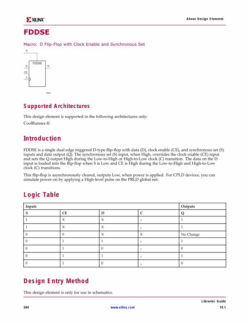
About Design Elements
FDDSE
Macro: D Flip-Flop with Clock Enable and Synchronous Set
Supported Architectures
This design element is supported in the following architectures only:CoolRunner-II
IntroductionFDDSE is a single dual edge triggered D-type flip-flop with data (D), clock enable (CE), and synchronous set (S)inputs and data output (Q). The synchronous set (S) input, when High, overrides the clock enable (CE) inputand sets the Q output High during the Low-to-High or High-to-Low clock (C) transition. The data on the Dinput is loaded into the flip-flop when S is Low and CE is High during the Low-to-High and High-to-Lowclock (C) transitions.
This flip-flop is asynchronously cleared, outputs Low, when power is applied. For CPLD devices, you cansimulate power-on by applying a High-level pulse on the PRLD global net.
Logic TableInputs Outputs
S CE D C Q
1 X X ↑ 1
1 X X ↓ 1
0 0 X X No Change
0 1 1 ↑ 1
0 1 0 ↑ 0
0 1 1 ↓ 1
0 1 0 ↓ 0
Design Entry MethodThis design element is only for use in schematics.
Libraries Guide
384 www.xilinx.com 10.1

About Design Elements
For More Information• See the appropriate CPLD User Guide.
• See the appropriate CPLD Data Sheets.
Libraries Guide
10.1 www.xilinx.com 385
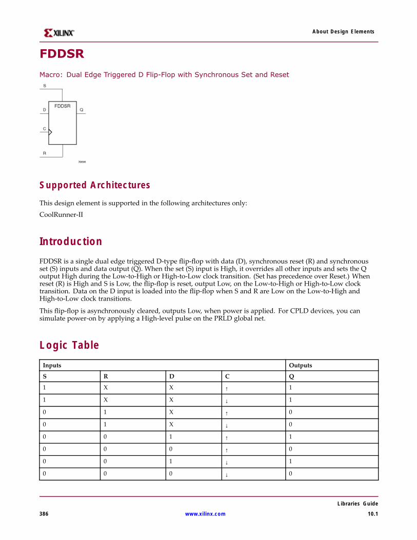
About Design Elements
FDDSR
Macro: Dual Edge Triggered D Flip-Flop with Synchronous Set and Reset
Supported Architectures
This design element is supported in the following architectures only:
CoolRunner-II
IntroductionFDDSR is a single dual edge triggered D-type flip-flop with data (D), synchronous reset (R) and synchronousset (S) inputs and data output (Q). When the set (S) input is High, it overrides all other inputs and sets the Qoutput High during the Low-to-High or High-to-Low clock transition. (Set has precedence over Reset.) Whenreset (R) is High and S is Low, the flip-flop is reset, output Low, on the Low-to-High or High-to-Low clocktransition. Data on the D input is loaded into the flip-flop when S and R are Low on the Low-to-High andHigh-to-Low clock transitions.
This flip-flop is asynchronously cleared, outputs Low, when power is applied. For CPLD devices, you cansimulate power-on by applying a High-level pulse on the PRLD global net.
Logic TableInputs Outputs
S R D C Q
1 X X ↑ 1
1 X X ↓ 1
0 1 X ↑ 0
0 1 X ↓ 0
0 0 1 ↑ 1
0 0 0 ↑ 0
0 0 1 ↓ 1
0 0 0 ↓ 0
Libraries Guide
386 www.xilinx.com 10.1

About Design Elements
Design Entry MethodThis design element is only for use in schematics.
For More Information• See the appropriate CPLD User Guide.
• See the appropriate CPLD Data Sheets.
Libraries Guide
10.1 www.xilinx.com 387

About Design Elements
FDDSRE
Macro: Dual Edge Triggered D Flip-Flop with Synchronous Set and Reset and Clock Enable
Supported Architectures
This design element is supported in the following architectures only:
CoolRunner-II
IntroductionFDDSRE is a single dual edge triggered D-type flip-flop with synchronous set (S), synchronous reset (R), andclock enable (CE) inputs and data output (Q). When synchronous set (S) is High, it overrides all other inputs andsets the Q output High during the Low-to-High or High-to-Low clock transition. (Set has precedence over Reset.)When synchronous reset (R) is High and S is Low, output Q is reset Low during the Low-to-High or High-to-Lowclock transition. Data is loaded into the flip-flop when S and R are Low and CE is High during the Low-to-Highand High-to-Low clock transitions. When CE is Low, clock transitions are ignored.
This flip-flop is asynchronously cleared, outputs Low, when power is applied. For CPLD devices, you cansimulate power-on by applying a High-level pulse on the PRLD global net.
Logic TableInputs Outputs
S R CE D C Q
1 X X X ↑ 1
1 X X X ↓ 1
0 1 X X ↑ 0
0 1 X X ↓ 0
0 0 0 X X No Change
0 0 1 1 ↑ 1
0 0 1 0 ↑ 0
0 0 1 1 ↓ 1
0 0 1 0 ↓ 0
Libraries Guide
388 www.xilinx.com 10.1

About Design Elements
Design Entry MethodThis design element is only for use in schematics.
For More Information• See the appropriate CPLD User Guide.
• See the appropriate CPLD Data Sheets.
Libraries Guide
10.1 www.xilinx.com 389

About Design Elements
FDPMacro: D Flip-Flop with Asynchronous Preset
Supported ArchitecturesThis design element is supported in the following architectures only:• XC9500XL• CoolRunner XPLA3• CoolRunner-II
IntroductionThis design element is a single D-type flip-flop with data (D) and asynchronous preset (PRE) inputs and dataoutput (Q). The asynchronous PRE, when High, overrides all other inputs and presets the (Q) output High. Thedata on the (D) input is loaded into the flip-flop when PRE is Low on the Low-to-High clock (C) transition.
For CPLD devices, this flip-flop is asynchronously cleared, output Low, when power is applied. You can simulatepower-on by applying a High-level pulse on the PRLD global net.
Logic TableInputs Outputs
PRE C D Q
1 X X 1
0 ↑ D D
0 ↑ 0 0
Design Entry MethodThis design element is only for use in schematics.
Available Attributes
Attribute TypeAllowedValues Default Description
INIT Binary 0 or 1 0 Sets the initial value of Q output after configuration.
Libraries Guide
390 www.xilinx.com 10.1

About Design Elements
For More Information• See the appropriate CPLD User Guide.
• See the appropriate CPLD Data Sheets.
Libraries Guide
10.1 www.xilinx.com 391

About Design Elements
FDPE
Primitive: D Flip-Flop with Clock Enable and Asynchronous Preset
Supported Architectures
This design element is supported in the following architectures only:
• XC9500XL
• CoolRunner XPLA3
• CoolRunner-II
IntroductionThis design element is a single D-type flip-flop with data (D), clock enable (CE), and asynchronous preset(PRE) inputs and data output (Q). The asynchronous PRE, when High, overrides all other inputs and sets the(Q) output High. Data on the (D) input is loaded into the flip-flop when PRE is Low and CE is High on theLow-to-High clock (C) transition. When CE is Low, the clock transitions are ignored.
For CPLD devices, this flip-flop is asynchronously cleared, output Low, when power is applied. You can simulatepower-on by applying a High-level pulse on the PRLD global net.
Logic TableInputs Outputs
PRE CE D C Q
1 X X X 1
0 0 X X No Change
0 1 D ↑ D
Design Entry MethodThis design element is only for use in schematics.
Libraries Guide
392 www.xilinx.com 10.1
About Design Elements
Available Attributes
Attribute TypeAllowedValues Default Description
INIT Binary 0 or 1 0 Sets the initial value of Q output after configuration
For More Information• See the appropriate CPLD User Guide.
• See the appropriate CPLD Data Sheets.
Libraries Guide
10.1 www.xilinx.com 393
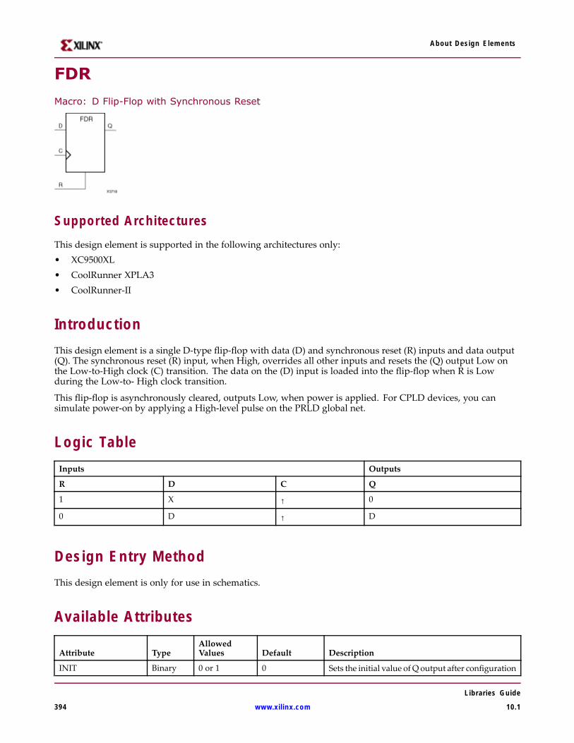
About Design Elements
FDR
Macro: D Flip-Flop with Synchronous Reset
Supported ArchitecturesThis design element is supported in the following architectures only:• XC9500XL• CoolRunner XPLA3• CoolRunner-II
IntroductionThis design element is a single D-type flip-flop with data (D) and synchronous reset (R) inputs and data output(Q). The synchronous reset (R) input, when High, overrides all other inputs and resets the (Q) output Low onthe Low-to-High clock (C) transition. The data on the (D) input is loaded into the flip-flop when R is Lowduring the Low-to- High clock transition.
This flip-flop is asynchronously cleared, outputs Low, when power is applied. For CPLD devices, you cansimulate power-on by applying a High-level pulse on the PRLD global net.
Logic TableInputs Outputs
R D C Q
1 X ↑ 0
0 D ↑ D
Design Entry MethodThis design element is only for use in schematics.
Available Attributes
Attribute TypeAllowedValues Default Description
INIT Binary 0 or 1 0 Sets the initial value ofQ output after configuration
Libraries Guide
394 www.xilinx.com 10.1

About Design Elements
For More Information• See the appropriate CPLD User Guide.
• See the appropriate CPLD Data Sheets.
Libraries Guide
10.1 www.xilinx.com 395

About Design Elements
FDRE
Macro: D Flip-Flop with Clock Enable and Synchronous Reset
Supported ArchitecturesThis design element is supported in the following architectures only:• XC9500XL• CoolRunner XPLA3• CoolRunner-II
IntroductionThis design element is a single D-type flip-flop with data (D), clock enable (CE), and synchronous reset (R) inputsand data output (Q). The synchronous reset (R) input, when High, overrides all other inputs and resets the (Q)output Low on the Low-to-High clock (C) transition. The data on the (D) input is loaded into the flip-flop when Ris Low and CE is High during the Low-to-High clock transition.
This flip-flop is asynchronously cleared, outputs Low, when power is applied. For CPLD devices, you cansimulate power-on by applying a High-level pulse on the PRLD global net.
Logic TableInputs Outputs
R CE D C Q
1 X X ↑ 0
0 0 X X No Change
0 1 D ↑ D
Design Entry MethodThis design element is only for use in schematics.
Available AttributesAttribute Type Allowed Values Default Description
INIT Binary 0 or 1 0 Sets the initial value of Q output after configuration.
Libraries Guide
396 www.xilinx.com 10.1

About Design Elements
For More Information• See the appropriate CPLD User Guide.
• See the appropriate CPLD Data Sheets.
Libraries Guide
10.1 www.xilinx.com 397

About Design Elements
FDRS
Macro: D Flip-Flop with Synchronous Reset and Set
Supported Architectures
This design element is supported in the following architectures only:
• XC9500XL
• CoolRunner XPLA3
• CoolRunner-II
IntroductionFDRS is a single D-type flip-flop with data (D), synchronous set (S), and synchronous reset (R) inputs and dataoutput (Q). The synchronous reset (R) input, when High, overrides all other inputs and resets the (Q) output Lowduring the Low-to-High clock (C) transition. (Reset has precedence over Set.) When S is High and R is Low, theflip-flop is set, output High, during the Low-to-High clock transition. When R and S are Low, data on the (D)input is loaded into the flip-flop during the Low-to-High clock transition.
This flip-flop is asynchronously cleared, outputs Low, when power is applied. For CPLD devices, you cansimulate power-on by applying a High-level pulse on the PRLD global net.
Logic TableInputs Outputs
R S D C Q
1 X X ↓ 0
0 1 X ↓ 1
0 0 D ↓ D
Design Entry MethodThis design element is only for use in schematics.
Libraries Guide
398 www.xilinx.com 10.1
About Design Elements
Available Attributes
Attribute TypeAllowedValues Default Description
IN Binary 0 or 1 0 Sets the initial value of Q output after configuration.
Libraries Guide
10.1 www.xilinx.com 399

About Design Elements
For More Information• See the appropriate CPLD User Guide.
• See the appropriate CPLD Data Sheets.
Libraries Guide
400 www.xilinx.com 10.1
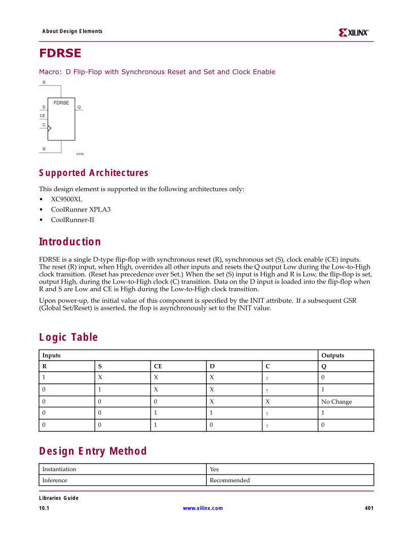
About Design Elements
FDRSEMacro: D Flip-Flop with Synchronous Reset and Set and Clock Enable
Supported ArchitecturesThis design element is supported in the following architectures only:• XC9500XL• CoolRunner XPLA3• CoolRunner-II
IntroductionFDRSE is a single D-type flip-flop with synchronous reset (R), synchronous set (S), clock enable (CE) inputs.The reset (R) input, when High, overrides all other inputs and resets the Q output Low during the Low-to-Highclock transition. (Reset has precedence over Set.) When the set (S) input is High and R is Low, the flip-flop is set,output High, during the Low-to-High clock (C) transition. Data on the D input is loaded into the flip-flop whenR and S are Low and CE is High during the Low-to-High clock transition.
Upon power-up, the initial value of this component is specified by the INIT attribute. If a subsequent GSR(Global Set/Reset) is asserted, the flop is asynchronously set to the INIT value.
Logic TableInputs Outputs
R S CE D C Q
1 X X X ↑ 0
0 1 X X ↑ 1
0 0 0 X X No Change
0 0 1 1 ↑ 1
0 0 1 0 ↑ 0
Design Entry MethodInstantiation Yes
Inference Recommended
Libraries Guide
10.1 www.xilinx.com 401

About Design Elements
Coregen and wizards No
Macro support No
This design element can be used in schematics.
Available AttributesAttribute Type Allowed Values Default Description
INIT Binary 0 or 1 0 Sets the initial value of Q output after configuration and on GSR.
VHDL Instantiation TemplateUnless they already exist, copy the following two statements and paste them before the entity declaration.Library UNISIM;use UNISIM.vcomponents.all;
-- FDRSE: Single Data Rate D Flip-Flop with Synchronous Clear, Set and-- Clock Enable (posedge clk). All families.-- Xilinx HDL Libraries Guide, version 10.1.2
FDRSE_inst : FDRSEgeneric map (INIT => ’0’) -- Initial value of register (’0’ or ’1’)port map (Q => Q, -- Data outputC => C, -- Clock inputCE => CE, -- Clock enable inputD => D, -- Data inputR => R, -- Synchronous reset inputS => S -- Synchronous set input);
-- End of FDRSE_inst instantiation
Verilog Instantiation Template// FDRSE: Single Data Rate D Flip-Flop with Synchronous Clear, Set and// Clock Enable (posedge clk).// All families.// Xilinx HDL Libraries Guide, version 10.1.2
FDRSE #(.INIT(1’b0) // Initial value of register (1’b0 or 1’b1)) FDRSE_inst (.Q(Q), // Data output.C(C), // Clock input.CE(CE), // Clock enable input.D(D), // Data input.R(R), // Synchronous reset input.S(S) // Synchronous set input);
// End of FDRSE_inst instantiation
For More Information• See the appropriate CPLD User Guide.
Libraries Guide
402 www.xilinx.com 10.1

About Design Elements
• See the appropriate CPLD Data Sheets.
Libraries Guide
10.1 www.xilinx.com 403

About Design Elements
FDSMacro: D Flip-Flop with Synchronous Set
Supported ArchitecturesThis design element is supported in the following architectures only:• XC9500XL• CoolRunner XPLA3• CoolRunner-II
IntroductionFDS is a single D-type flip-flop with data (D) and synchronous set (S) inputs and data output (Q). Thesynchronous set input, when High, sets the Q output High on the Low-to-High clock (C) transition. The data onthe D input is loaded into the flip-flop when S is Low during the Low-to-High clock (C) transition.
For CPLD devices, this flip-flop is asynchronously cleared, output Low, when power is applied. You can simulatepower-on by applying a High-level pulse on the PRLD global net.
Logic Table
Inputs Outputs
S D C Q
1 X ↑ 1
0 D ↑ D
Design Entry MethodThis design element is only for use in schematics.
Available Attributes
Attribute TypeAllowedValues Default Description
INIT Binary 0 or 1 0 Sets the initial value of Q output after configuration.
Libraries Guide
404 www.xilinx.com 10.1

About Design Elements
For More Information• See the appropriate CPLD User Guide.
• See the appropriate CPLD Data Sheets.
Libraries Guide
10.1 www.xilinx.com 405
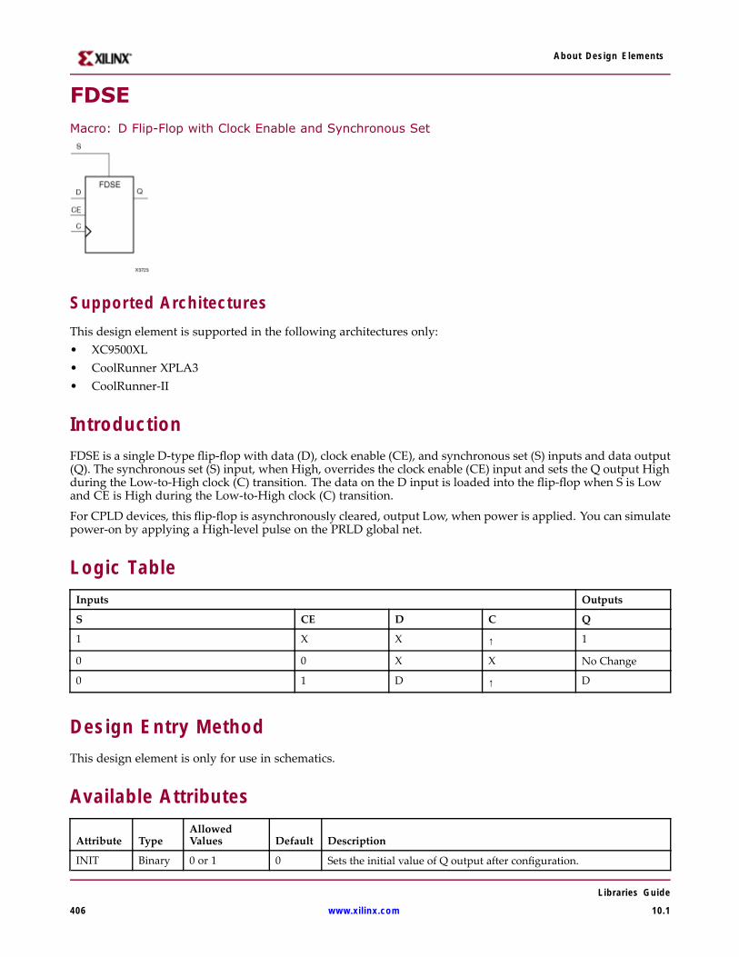
About Design Elements
FDSEMacro: D Flip-Flop with Clock Enable and Synchronous Set
Supported ArchitecturesThis design element is supported in the following architectures only:• XC9500XL• CoolRunner XPLA3• CoolRunner-II
IntroductionFDSE is a single D-type flip-flop with data (D), clock enable (CE), and synchronous set (S) inputs and data output(Q). The synchronous set (S) input, when High, overrides the clock enable (CE) input and sets the Q output Highduring the Low-to-High clock (C) transition. The data on the D input is loaded into the flip-flop when S is Lowand CE is High during the Low-to-High clock (C) transition.
For CPLD devices, this flip-flop is asynchronously cleared, output Low, when power is applied. You can simulatepower-on by applying a High-level pulse on the PRLD global net.
Logic TableInputs Outputs
S CE D C Q
1 X X ↑ 1
0 0 X X No Change
0 1 D ↑ D
Design Entry MethodThis design element is only for use in schematics.
Available Attributes
Attribute TypeAllowedValues Default Description
INIT Binary 0 or 1 0 Sets the initial value of Q output after configuration.
Libraries Guide
406 www.xilinx.com 10.1

About Design Elements
For More Information• See the appropriate CPLD User Guide.
• See the appropriate CPLD Data Sheets.
Libraries Guide
10.1 www.xilinx.com 407

About Design Elements
FDSR
Macro: D Flip-Flop with Synchronous Set and Reset
Supported Architectures
This design element is supported in the following architectures only:
• XC9500XL
• CoolRunner XPLA3
• CoolRunner-II
IntroductionFDSR is a single D-type flip-flop with data (D), synchronous reset (R) and synchronous set (S) inputs and dataoutput (Q). When the set (S) input is High, it overrides all other inputs and sets the Q output High during theLow-to-High clock transition. (Set has precedence over Reset.) When reset (R) is High and S is Low, the flip-flopis reset, output Low, on the Low-to-High clock transition. Data on the D input is loaded into the flip-flop when Sand R are Low on the Low-to-High clock transition.
This flip-flop is asynchronously cleared, outputs Low, when power is applied. For CPLD devices, you cansimulate power-on by applying a High-level pulse on the PRLD global net.
Logic TableInputs Outputs
S R D C Q
1 X X ↑ 1
0 1 X ↑ 0
0 0 1 ↑ 1
0 0 0 ↑ 0
Design Entry MethodThis design element is only for use in schematics.
Libraries Guide
408 www.xilinx.com 10.1

About Design Elements
For More Information• See the appropriate CPLD User Guide.
• See the appropriate CPLD Data Sheets.
Libraries Guide
10.1 www.xilinx.com 409

About Design Elements
FDSRE
Macro: D Flip-Flop with Synchronous Set and Reset and Clock Enable
Supported ArchitecturesThis design element is supported in the following architectures only:• XC9500XL• CoolRunner XPLA3• CoolRunner-II
IntroductionFDSRE is a single D-type flip-flop with synchronous set (S), synchronous reset (R), and clock enable (CE) inputsand data output (Q). When synchronous set (S) is High, it overrides all other inputs and sets the Q outputHigh during the Low-to-High clock transition. (Set has precedence over Reset.) When synchronous reset (R)is High and S is Low, output Q is reset Low during the Low-to-High clock transition. Data is loaded into theflip-flop when S and R are Low and CE is High during the Low-to-high clock transition. When CE is Low,clock transitions are ignored.
This flip-flop is asynchronously cleared, outputs Low, when power is applied. For CPLD devices, you cansimulate power-on by applying a High-level pulse on the PRLD global net.
Logic TableInputs Outputs
S R CE D C Q
1 X X X ↑ 1
0 1 X X ↑ 0
0 0 0 X X No Change
0 0 1 1 ↑ 1
0 0 1 0 ↑ 0
Design Entry MethodThis design element is only for use in schematics.
Libraries Guide
410 www.xilinx.com 10.1

About Design Elements
For More Information• See the appropriate CPLD User Guide.
• See the appropriate CPLD Data Sheets.
Libraries Guide
10.1 www.xilinx.com 411
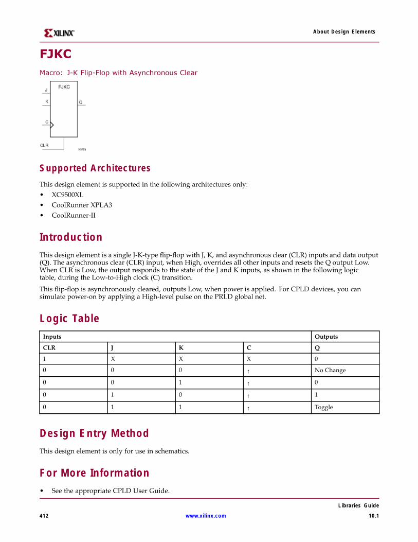
About Design Elements
FJKCMacro: J-K Flip-Flop with Asynchronous Clear
Supported ArchitecturesThis design element is supported in the following architectures only:• XC9500XL• CoolRunner XPLA3• CoolRunner-II
IntroductionThis design element is a single J-K-type flip-flop with J, K, and asynchronous clear (CLR) inputs and data output(Q). The asynchronous clear (CLR) input, when High, overrides all other inputs and resets the Q output Low.When CLR is Low, the output responds to the state of the J and K inputs, as shown in the following logictable, during the Low-to-High clock (C) transition.
This flip-flop is asynchronously cleared, outputs Low, when power is applied. For CPLD devices, you cansimulate power-on by applying a High-level pulse on the PRLD global net.
Logic TableInputs Outputs
CLR J K C Q
1 X X X 0
0 0 0 ↑ No Change
0 0 1 ↑ 0
0 1 0 ↑ 1
0 1 1 ↑ Toggle
Design Entry MethodThis design element is only for use in schematics.
For More Information• See the appropriate CPLD User Guide.
Libraries Guide
412 www.xilinx.com 10.1

About Design Elements
• See the appropriate CPLD Data Sheets.
Libraries Guide
10.1 www.xilinx.com 413

About Design Elements
FJKCE
Macro: J-K Flip-Flop with Clock Enable and Asynchronous Clear
Supported Architectures
This design element is supported in the following architectures only:• XC9500XL• CoolRunner XPLA3• CoolRunner-II
IntroductionThis design element is a single J-K-type flip-flop with J, K, clock enable (CE), and asynchronous clear (CLR)inputs and data output (Q). The asynchronous clear (CLR), when High, overrides all other inputs and resets theQ output Low. When CLR is Low and CE is High, Q responds to the state of the J and K inputs, as shown in thefollowing logic table, during the Low-to-High clock transition. When CE is Low, the clock transitions are ignored.
This flip-flop is asynchronously cleared, outputs Low, when power is applied. For CPLD devices, you cansimulate power-on by applying a High-level pulse on the PRLD global net.
Logic TableInputs Outputs
CLR CE J K C Q
1 X X X X 0
0 0 X X X No Change
0 1 0 0 X No Change
0 1 0 1 ↑ 0
0 1 1 0 ↑ 1
0 1 1 1 ↑ Toggle
Design Entry MethodThis design element is only for use in schematics.
Libraries Guide
414 www.xilinx.com 10.1

About Design Elements
For More Information• See the appropriate CPLD User Guide.
• See the appropriate CPLD Data Sheets.
Libraries Guide
10.1 www.xilinx.com 415
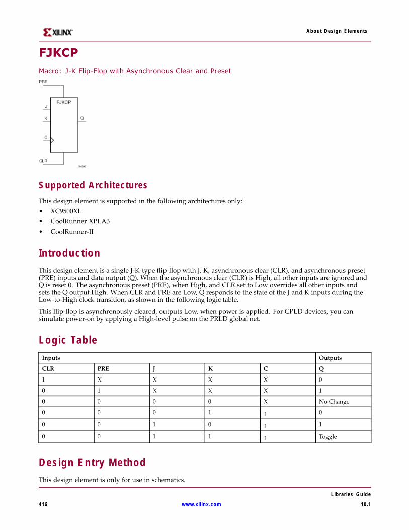
About Design Elements
FJKCPMacro: J-K Flip-Flop with Asynchronous Clear and Preset
Supported ArchitecturesThis design element is supported in the following architectures only:• XC9500XL• CoolRunner XPLA3• CoolRunner-II
IntroductionThis design element is a single J-K-type flip-flop with J, K, asynchronous clear (CLR), and asynchronous preset(PRE) inputs and data output (Q). When the asynchronous clear (CLR) is High, all other inputs are ignored andQ is reset 0. The asynchronous preset (PRE), when High, and CLR set to Low overrides all other inputs andsets the Q output High. When CLR and PRE are Low, Q responds to the state of the J and K inputs during theLow-to-High clock transition, as shown in the following logic table.
This flip-flop is asynchronously cleared, outputs Low, when power is applied. For CPLD devices, you cansimulate power-on by applying a High-level pulse on the PRLD global net.
Logic TableInputs Outputs
CLR PRE J K C Q
1 X X X X 0
0 1 X X X 1
0 0 0 0 X No Change
0 0 0 1 ↑ 0
0 0 1 0 ↑ 1
0 0 1 1 ↑ Toggle
Design Entry MethodThis design element is only for use in schematics.
Libraries Guide
416 www.xilinx.com 10.1

About Design Elements
For More Information• See the appropriate CPLD User Guide.
• See the appropriate CPLD Data Sheets.
Libraries Guide
10.1 www.xilinx.com 417

About Design Elements
FJKCPE
Macro: J-K Flip-Flop with Asynchronous Clear and Preset and Clock Enable
Supported Architectures
This design element is supported in the following architectures only:• XC9500XL• CoolRunner XPLA3• CoolRunner-II
IntroductionThis design element is a single J-K-type flip-flop with J, K, asynchronous clear (CLR), asynchronous preset(PRE), and clock enable (CE) inputs and data output (Q). When the asynchronous clear (CLR) is High, all otherinputs are ignored and Q is reset 0. The asynchronous preset (PRE), when High, and CLR set to Low overridesall other inputs and sets the Q output High. When CLR and PRE are Low and CE is High, Q responds to thestate of the J and K inputs, as shown in the following logic table, during the Low-to-High clock transition. Clocktransitions are ignored when CE is Low.
This flip-flop is asynchronously cleared, outputs Low, when power is applied. For CPLD devices, you cansimulate power-on by applying a High-level pulse on the PRLD global net.
Logic TableInputs Outputs
CLR PRE CE J K C Q
1 X X X X X 0
0 1 X X X X 1
0 0 0 0 X X No Change
0 0 1 0 0 X No Change
0 0 1 0 1 ¦ 0
0 0 1 1 0 ¦ 1
0 0 1 1 1 ¦ Toggle
Libraries Guide
418 www.xilinx.com 10.1

About Design Elements
Design Entry MethodThis design element is only for use in schematics.
For More Information• See the appropriate CPLD User Guide.
• See the appropriate CPLD Data Sheets.
Libraries Guide
10.1 www.xilinx.com 419

About Design Elements
FJKP
Macro: J-K Flip-Flop with Asynchronous Preset
Supported Architectures
This design element is supported in the following architectures only:• XC9500XL• CoolRunner XPLA3• CoolRunner-II
IntroductionThis design element is a single J-K-type flip-flop with J, K, and asynchronous preset (PRE) inputs and dataoutput (Q). The asynchronous preset (PRE) input, when High, overrides all other inputs and sets the (Q) outputHigh. When (PRE) is Low, the (Q) output responds to the state of the J and K inputs, as shown in the followinglogic table, during the Low-to-High clock transition.
For CPLD devices, this flip-flop is asynchronously cleared, output Low, when power is applied. You can simulatepower-on by applying a High-level pulse on the PRLD global net.
Logic TableInputs Outputs
PRE J K C Q
1 X X X 1
0 0 0 X No Change
0 0 1 ↑ 0
0 1 0 ↑ 1
0 1 1 ↑ Toggle
Design Entry MethodThis design element is only for use in schematics.
Libraries Guide
420 www.xilinx.com 10.1

About Design Elements
For More Information• See the appropriate CPLD User Guide.
• See the appropriate CPLD Data Sheets.
Libraries Guide
10.1 www.xilinx.com 421
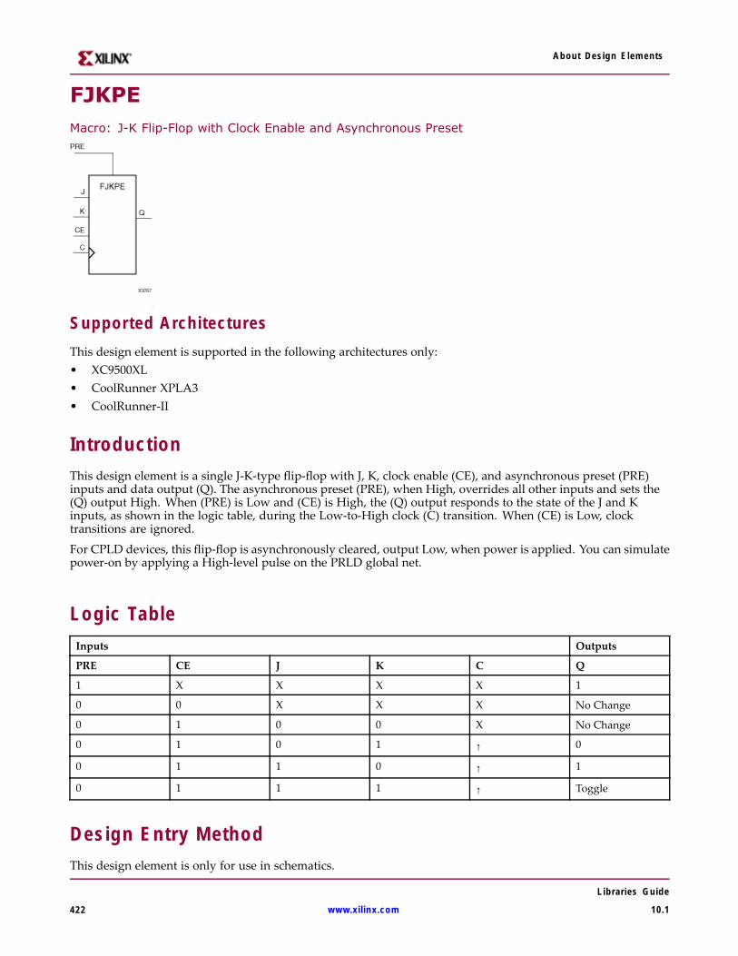
About Design Elements
FJKPEMacro: J-K Flip-Flop with Clock Enable and Asynchronous Preset
Supported ArchitecturesThis design element is supported in the following architectures only:• XC9500XL• CoolRunner XPLA3• CoolRunner-II
IntroductionThis design element is a single J-K-type flip-flop with J, K, clock enable (CE), and asynchronous preset (PRE)inputs and data output (Q). The asynchronous preset (PRE), when High, overrides all other inputs and sets the(Q) output High. When (PRE) is Low and (CE) is High, the (Q) output responds to the state of the J and Kinputs, as shown in the logic table, during the Low-to-High clock (C) transition. When (CE) is Low, clocktransitions are ignored.
For CPLD devices, this flip-flop is asynchronously cleared, output Low, when power is applied. You can simulatepower-on by applying a High-level pulse on the PRLD global net.
Logic TableInputs Outputs
PRE CE J K C Q
1 X X X X 1
0 0 X X X No Change
0 1 0 0 X No Change
0 1 0 1 ↑ 0
0 1 1 0 ↑ 1
0 1 1 1 ↑ Toggle
Design Entry MethodThis design element is only for use in schematics.
Libraries Guide
422 www.xilinx.com 10.1

About Design Elements
For More Information• See the appropriate CPLD User Guide.
• See the appropriate CPLD Data Sheets.
Libraries Guide
10.1 www.xilinx.com 423

About Design Elements
FJKRSE
Macro: J-K Flip-Flop with Clock Enable and Synchronous Reset and Set
Supported Architectures
This design element is supported in the following architectures only:• XC9500XL• CoolRunner XPLA3• CoolRunner-II
IntroductionThis design element is a single J-K-type flip-flop with J, K, synchronous reset (R), synchronous set (S), and clockenable (CE) inputs and data output (Q). When synchronous reset (R) is High during the Low-to-High clock (C)transition, all other inputs are ignored and output (Q) is reset Low. When synchronous set (S) is High and (R) isLow, output (Q) is set High. When (R) and (S) are Low and (CE) is High, output (Q) responds to the state ofthe J and K inputs, according to the following logic table, during the Low-to-High clock (C) transition. When(CE) is Low, clock transitions are ignored.
This flip-flop is asynchronously cleared, outputs Low, when power is applied. For CPLD devices, you cansimulate power-on by applying a High-level pulse on the PRLD global net.
Logic TableInputs Outputs
R S CE J K C Q
1 X X X X ↑ 0
0 1 X X X ↑ 1
0 0 0 X X X No Change
0 0 1 0 0 X No Change
0 0 1 0 1 ↑ 0
0 0 1 1 1 ↑ Toggle
0 0 1 1 0 ↑ 1
Libraries Guide
424 www.xilinx.com 10.1

About Design Elements
Design Entry MethodThis design element is only for use in schematics.
For More Information• See the appropriate CPLD User Guide.
• See the appropriate CPLD Data Sheets.
Libraries Guide
10.1 www.xilinx.com 425
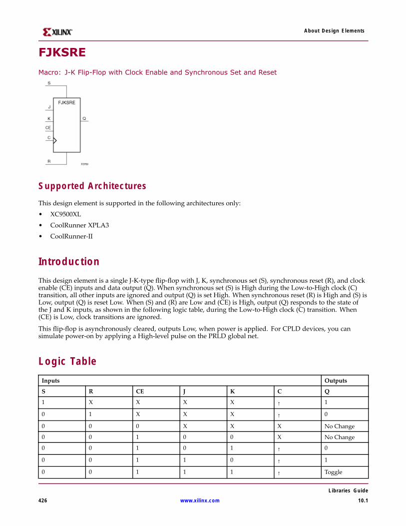
About Design Elements
FJKSRE
Macro: J-K Flip-Flop with Clock Enable and Synchronous Set and Reset
Supported Architectures
This design element is supported in the following architectures only:• XC9500XL• CoolRunner XPLA3• CoolRunner-II
IntroductionThis design element is a single J-K-type flip-flop with J, K, synchronous set (S), synchronous reset (R), and clockenable (CE) inputs and data output (Q). When synchronous set (S) is High during the Low-to-High clock (C)transition, all other inputs are ignored and output (Q) is set High. When synchronous reset (R) is High and (S) isLow, output (Q) is reset Low. When (S) and (R) are Low and (CE) is High, output (Q) responds to the state ofthe J and K inputs, as shown in the following logic table, during the Low-to-High clock (C) transition. When(CE) is Low, clock transitions are ignored.
This flip-flop is asynchronously cleared, outputs Low, when power is applied. For CPLD devices, you cansimulate power-on by applying a High-level pulse on the PRLD global net.
Logic TableInputs Outputs
S R CE J K C Q
1 X X X X ↑ 1
0 1 X X X ↑ 0
0 0 0 X X X No Change
0 0 1 0 0 X No Change
0 0 1 0 1 ↑ 0
0 0 1 1 0 ↑ 1
0 0 1 1 1 ↑ Toggle
Libraries Guide
426 www.xilinx.com 10.1

About Design Elements
Design Entry MethodThis design element is only for use in schematics.
For More Information• See the appropriate CPLD User Guide.
• See the appropriate CPLD Data Sheets.
Libraries Guide
10.1 www.xilinx.com 427

About Design Elements
FTC
Primitive: Toggle Flip-Flop with Asynchronous Clear
Supported Architectures
This design element is supported in the following architectures only:• XC9500XL• CoolRunner XPLA3• CoolRunner-II
IntroductionThis design element is a synchronous, resettable toggle flip-flop. The asynchronous clear (CLR) input, whenHigh, overrides all other inputs and resets the data output (Q) Low. The (Q) output toggles, or changes state,when the toggle enable (T) input is High and (CLR) is Low during the Low-to-High clock transition.
This flip-flop is asynchronously cleared, outputs Low, when power is applied. For CPLD devices, you cansimulate power-on by applying a High-level pulse on the PRLD global net.
Logic TableInputs Outputs
CLR T C Q
1 X X 0
0 0 X No Change
0 1 ↑ Toggle
Design Entry MethodYou can instantiate this element when targeting a CPLD, but not when you are targeting an FPGA.
For More Information• See the appropriate CPLD User Guide.• See the appropriate CPLD Data Sheets.
Libraries Guide
428 www.xilinx.com 10.1

About Design Elements
FTCE
Macro: Toggle Flip-Flop with Clock Enable and Asynchronous Clear
Supported ArchitecturesThis design element is supported in the following architectures only:• XC9500XL• CoolRunner XPLA3• CoolRunner-II
IntroductionThis design element is a toggle flip-flop with toggle and clock enable and asynchronous clear. When theasynchronous clear (CLR) input is High, all other inputs are ignored and the data output (Q) is reset Low. WhenCLR is Low and toggle enable (T) and clock enable (CE) are High, Q output toggles, or changes state, during theLow-to-High clock (C) transition. When CE is Low, clock transitions are ignored.
This flip-flop is asynchronously cleared, outputs Low, when power is applied. For CPLD devices, you cansimulate power-on by applying a High-level pulse on the PRLD global net.
Logic TableInputs Outputs
CLR CE T C Q
1 X X X 0
0 0 X X No Change
0 1 0 X No Change
0 1 1 ↑ Toggle
Design Entry MethodThis design element is only for use in schematics.
For More Information• See the appropriate CPLD User Guide.• See the appropriate CPLD Data Sheets.
Libraries Guide
10.1 www.xilinx.com 429

About Design Elements
FTCLE
Macro: Toggle/Loadable Flip-Flop with Clock Enable and Asynchronous Clear
Supported ArchitecturesThis design element is supported in the following architectures only:• XC9500XL• CoolRunner XPLA3• CoolRunner-II
IntroductionThis design element is a toggle/loadable flip-flop with toggle and clock enable and asynchronous clear. Whenthe asynchronous clear input (CLR) is High, all other inputs are ignored and output Q is reset Low. When loadenable input (L) is High and CLR is Low, clock enable (CE) is overridden and the data on data input (D) isloaded into the flip-flop during the Low-to-High clock (C) transition. When toggle enable (T) and CE are Highand L and CLR are Low, output Q toggles, or changes state, during the Low- to-High clock transition. WhenCE is Low, clock transitions are ignored.
This flip-flop is asynchronously cleared, outputs Low, when power is applied. For CPLD devices, you cansimulate power-on by applying a High-level pulse on the PRLD global net.
Logic TableInputs Outputs
CLR L CE T D C Q
1 X X X X X 0
0 1 X X D ↑ D
0 0 0 X X X No Change
0 0 1 0 X X No Change
0 0 1 1 X ↑ Toggle
Design Entry MethodThis design element is only for use in schematics.
Libraries Guide
430 www.xilinx.com 10.1

About Design Elements
For More Information• See the appropriate CPLD User Guide.
• See the appropriate CPLD Data Sheets.
Libraries Guide
10.1 www.xilinx.com 431

About Design Elements
FTCLEXMacro: Toggle/Loadable Flip-Flop with Clock Enable and Asynchronous Clear
Supported ArchitecturesThis design element is supported in the following architectures only:• XC9500XL• CoolRunner XPLA3• CoolRunner-II
IntroductionThis design element is a toggle/loadable flip-flop with toggle and clock enable and asynchronous clear. Whenthe asynchronous clear input (CLR) is High, all other inputs are ignored and output Q is reset Low. When loadenable input (L) is High, CLR is Low, and CE is High, the data on data input (D) is loaded into the flip-flop duringthe Low-to-High clock (C) transition. When toggle enable (T) and CE are High and L and CLR are Low, output Qtoggles, or changes state, during the Low- to-High clock transition. When CE is Low, clock transitions are ignored.
This flip-flop is asynchronously cleared, outputs Low, when power is applied. For CPLD devices, you cansimulate power-on by applying a High-level pulse on the PRLD global net.
Logic TableInputs Outputs
CLR L CE T D C Q
1 X X X X X 0
0 1 X X D ↑ D
0 0 0 X X X No Change
0 0 1 0 X X No Change
0 0 1 1 X ↑ Toggle
Design Entry MethodThis design element is only for use in schematics.
Libraries Guide
432 www.xilinx.com 10.1

About Design Elements
For More Information• See the appropriate CPLD User Guide.
• See the appropriate CPLD Data Sheets.
Libraries Guide
10.1 www.xilinx.com 433

About Design Elements
FTCPPrimitive: Toggle Flip-Flop with Asynchronous Clear and Preset
Supported ArchitecturesThis design element is supported in the following architectures only:• XC9500XL• CoolRunner XPLA3• CoolRunner-II
IntroductionThis design element is a toggle flip-flop with toggle enable and asynchronous clear and preset. When theasynchronous clear (CLR) input is High, all other inputs are ignored and the output (Q) is reset Low. Whenthe asynchronous preset (PRE) is High and CLR is Low, all other inputs are ignored and Q is set High. Whenthe toggle enable input (T) is High and CLR and PRE are Low, output Q toggles, or changes state, during theLow-to-High clock (C) transition.
This flip-flop is asynchronously cleared, outputs Low, when power is applied. For CPLD devices, you cansimulate power-on by applying a High-level pulse on the PRLD global net.
Logic TableInputs Outputs
CLR PRE T C Q
1 X X X 0
0 1 X X 1
0 0 0 X No Change
0 0 1 ↑ Toggle
Design Entry MethodThis design element is only for use in schematics.
Libraries Guide
434 www.xilinx.com 10.1

About Design Elements
For More Information• See the appropriate CPLD User Guide.
• See the appropriate CPLD Data Sheets.
Libraries Guide
10.1 www.xilinx.com 435

About Design Elements
FTCPEMacro: Toggle Flip-Flop with Clock Enable and Asynchronous Clear and Preset
Supported ArchitecturesThis design element is supported in the following architectures only:• XC9500XL• CoolRunner XPLA3• CoolRunner-II
IntroductionThis design element is a toggle flip-flop with toggle and clock enable and asynchronous clear and preset. Whenthe asynchronous clear (CLR) input is High, all other inputs are ignored and the output (Q) is reset Low. Whenthe asynchronous preset (PRE) is High and CLR is Low, all other inputs are ignored and Q is set High. When thetoggle enable input (T) and the clock enable input (CE) are High and CLR and PRE are Low, output Q toggles, orchanges state, during the Low-to-High clock (C) transition. Clock transitions are ignored when CE is Low.
This flip-flop is asynchronously cleared, outputs Low, when power is applied. For CPLD devices, you cansimulate power-on by applying a High-level pulse on the PRLD global net.
Logic TableInputs Outputs
CLR PRE CE T C Q
1 X X X X 0
0 1 X X X 1
0 0 0 X X No Change
0 0 1 0 X No Change
0 0 1 1 ↑ Toggle
Design Entry MethodThis design element is only for use in schematics.
For More Information• See the appropriate CPLD User Guide.• See the appropriate CPLD Data Sheets.
Libraries Guide
436 www.xilinx.com 10.1
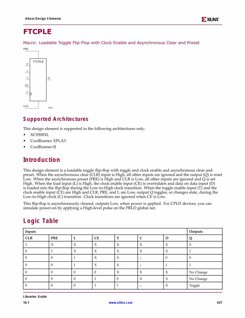
About Design Elements
FTCPLEMacro: Loadable Toggle Flip-Flop with Clock Enable and Asynchronous Clear and Preset
Supported ArchitecturesThis design element is supported in the following architectures only:• XC9500XL• CoolRunner XPLA3• CoolRunner-II
IntroductionThis design element is a loadable toggle flip-flop with toggle and clock enable and asynchronous clear andpreset. When the asynchronous clear (CLR) input is High, all other inputs are ignored and the output (Q) is resetLow. When the asynchronous preset (PRE) is High and CLR is Low, all other inputs are ignored and Q is setHigh. When the load input (L) is High, the clock enable input (CE) is overridden and data on data input (D)is loaded into the flip-flop during the Low-to-High clock transition. When the toggle enable input (T) and theclock enable input (CE) are High and CLR, PRE, and L are Low, output Q toggles, or changes state, during theLow-to-High clock (C) transition. Clock transitions are ignored when CE is Low.
This flip-flop is asynchronously cleared, outputs Low, when power is applied. For CPLD devices, you cansimulate power-on by applying a High-level pulse on the PRLD global net.
Logic TableInputs Outputs
CLR PRE L CE T C D Q
1 X X X X X X 0
0 1 X X X X X 1
0 0 1 X X ↑ 0 0
0 0 1 X X ↑ 1 1
0 0 0 0 X X X No Change
0 0 0 1 0 X X No Change
0 0 0 1 1 ↑ X Toggle
Libraries Guide
10.1 www.xilinx.com 437

About Design Elements
Design Entry MethodThis design element is only for use in schematics.
For More Information• See the appropriate CPLD User Guide.
• See the appropriate CPLD Data Sheets.
Libraries Guide
438 www.xilinx.com 10.1

About Design Elements
FTDCE
Macro: Dual-Edge Triggered Toggle Flip-Flop with Clock Enable and Asynchronous Clear
Supported ArchitecturesThis design element is supported in the following architectures only:CoolRunner-II
IntroductionThis design element is a dual edge triggered toggle flip-flop with toggle and clock enable and asynchronous clear.When the asynchronous clear (CLR) input is High, all other inputs are ignored and the data output (Q) is resetLow. When CLR is Low and toggle enable (T) and clock enable (CE) are High, Q output toggles, or changes state,during the Low-to-High and High-to-Low clock (C) transitions. When CE is Low, clock transitions are ignored.
This flip-flop is asynchronously cleared, outputs Low, when power is applied. For CPLD devices, you cansimulate power-on by applying a High-level pulse on the PRLD global net.
Logic TableInputs Outputs
CLR CE T C Q
1 X X X 0
0 0 X X No Change
0 1 0 X No Change
0 1 1 ↑ Toggle
0 1 1 ↓ Toggle
Design Entry MethodThis design element is only for use in schematics.
For More Information• See the appropriate CPLD User Guide.• See the appropriate CPLD Data Sheets.
Libraries Guide
10.1 www.xilinx.com 439

About Design Elements
FTDCLE
Macro: Dual-Edge Triggered Toggle/Loadable Flip-Flop with Clock Enable and Asynchronous Clear
Supported Architectures
This design element is supported in the following architectures only:
CoolRunner-II
IntroductionThis design element is a dual edge triggered toggle/loadable flip-flop with toggle and clock enable andasynchronous clear. When the asynchronous clear input (CLR) is High, all other inputs are ignored and output Qis reset Low. When load enable input (L) is High and CLR is Low, clock enable (CE) is overridden and the dataon data input (D) is loaded into the flip-flop during the Low-to-High and High-to-Low clock (C) transitions.When toggle enable (T) and CE are High and L and CLR are Low, output Q toggles, or changes state, during theLow- to-High and High-to-Low clock transitions. When CE is Low, clock transitions are ignored.
This flip-flop is asynchronously cleared, outputs Low, when power is applied. For CPLD devices, you cansimulate power-on by applying a High-level pulse on the PRLD global net.
Logic TableInputs Outputs
CLR L CE T D C Q
1 X X X X X 0
0 1 X X 1 ↑ 1
0 1 X X 1 ↓ 1
0 1 X X 0 ↑ 0
0 1 X X 0 ↓ 0
0 0 0 X X X No Change
0 0 1 0 X X No Change
0 0 1 1 X ↑ Toggle
0 0 1 1 X ↓ Toggle
Libraries Guide
440 www.xilinx.com 10.1

About Design Elements
Design Entry MethodThis design element is only for use in schematics.
For More Information• See the appropriate CPLD User Guide.
• See the appropriate CPLD Data Sheets.
Libraries Guide
10.1 www.xilinx.com 441

About Design Elements
FTDCLEX
Macro: Dual-Edge Triggered Toggle/Loadable Flip-Flop with Clock Enable and Asynchronous Clear
Supported ArchitecturesThis design element is supported in the following architectures only:CoolRunner-II
IntroductionThis design element is a dual edge triggered toggle/loadable flip-flop with toggle and clock enable andasynchronous clear. When the asynchronous clear input (CLR) is High, all other inputs are ignored and output Qis reset Low. When load enable input (L) is High, CLR is Low, and CE is High, the data on data input (D) isloaded into the flip-flop during the Low-to-High and High-to-Low clock (C) transitions. When toggle enable(T) and CE are High and L and CLR are Low, output Q toggles, or changes state, during the Low- to-High andHigh-to-Low clock transitions. When CE is Low, clock transitions are ignored.
This flip-flop is asynchronously cleared, outputs Low, when power is applied. For CPLD devices, you cansimulate power-on by applying a High-level pulse on the PRLD global net.
Logic TableInputs Outputs
CLR L CE T D C Q
1 X X X X X 0
0 1 1 X 1 ↑ 1
0 1 1 X 1 ↓ 1
0 1 1 X 0 ↑ 0
0 1 1 X 0 ↓ 0
0 0 0 X X X No Change
0 0 1 0 X X No Change
0 0 1 1 X ↑ Toggle
0 0 1 1 X ↓ Toggle
Libraries Guide
442 www.xilinx.com 10.1

About Design Elements
Design Entry MethodThis design element is only for use in schematics.
For More Information• See the appropriate CPLD User Guide.
• See the appropriate CPLD Data Sheets.
Libraries Guide
10.1 www.xilinx.com 443
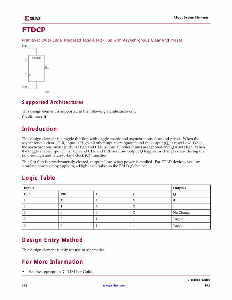
About Design Elements
FTDCPPrimitive: Dual-Edge Triggered Toggle Flip-Flop with Asynchronous Clear and Preset
Supported ArchitecturesThis design element is supported in the following architectures only:CoolRunner-II
IntroductionThis design element is a toggle flip-flop with toggle enable and asynchronous clear and preset. When theasynchronous clear (CLR) input is High, all other inputs are ignored and the output (Q) is reset Low. Whenthe asynchronous preset (PRE) is High and CLR is Low, all other inputs are ignored and Q is set High. Whenthe toggle enable input (T) is High and CLR and PRE are Low, output Q toggles, or changes state, during theLow-to-High and High-to-Low clock (C) transition.
This flip-flop is asynchronously cleared, outputs Low, when power is applied. For CPLD devices, you cansimulate power-on by applying a High-level pulse on the PRLD global net.
Logic TableInputs Outputs
CLR PRE T C Q
1 X X X 0
0 1 X X 1
0 0 0 X No Change
0 0 1 ↑ Toggle
0 0 1 ↓ Toggle
Design Entry MethodThis design element is only for use in schematics.
For More Information• See the appropriate CPLD User Guide.
Libraries Guide
444 www.xilinx.com 10.1
About Design Elements
• See the appropriate CPLD Data Sheets.
Libraries Guide
10.1 www.xilinx.com 445

About Design Elements
FTDRSEMacro: Dual-Edge Triggered Toggle Flip-Flop with Synchronous Reset, Set, and Clock Enable
Supported ArchitecturesThis design element is supported in the following architectures only:CoolRunner-II
IntroductionThis design element is a dual edge triggered toggle flip-flop with toggle and clock enable and synchronous resetand set. When the synchronous reset input (R) is High, it overrides all other inputs and the data output (Q) isreset Low. When the synchronous set input (S) is High and R is Low, clock enable input (CE) is overridden andoutput Q is set High. (Reset has precedence over Set.) When toggle enable input (T) and CE are High and R andS are Low, output Q toggles, or changes state, during the Low-to-High and High-to-Low clock transitions.
This flip-flop is asynchronously cleared, outputs Low, when power is applied. For CPLD devices, you cansimulate power-on by applying a High-level pulse on the PRLD global net.
Logic TableInputs Outputs
R S CE T C Q
1 X X X ↑ 0
1 X X X ↓ 0
0 1 X X ↑ 1
0 1 X X ↓ 1
0 0 0 X X No Change
0 0 1 0 X No Change
0 0 1 1 ↑ Toggle
0 0 1 1 ↓ Toggle
Design Entry MethodThis design element is only for use in schematics.
Libraries Guide
446 www.xilinx.com 10.1

About Design Elements
For More Information• See the appropriate CPLD User Guide.
• See the appropriate CPLD Data Sheets.
Libraries Guide
10.1 www.xilinx.com 447
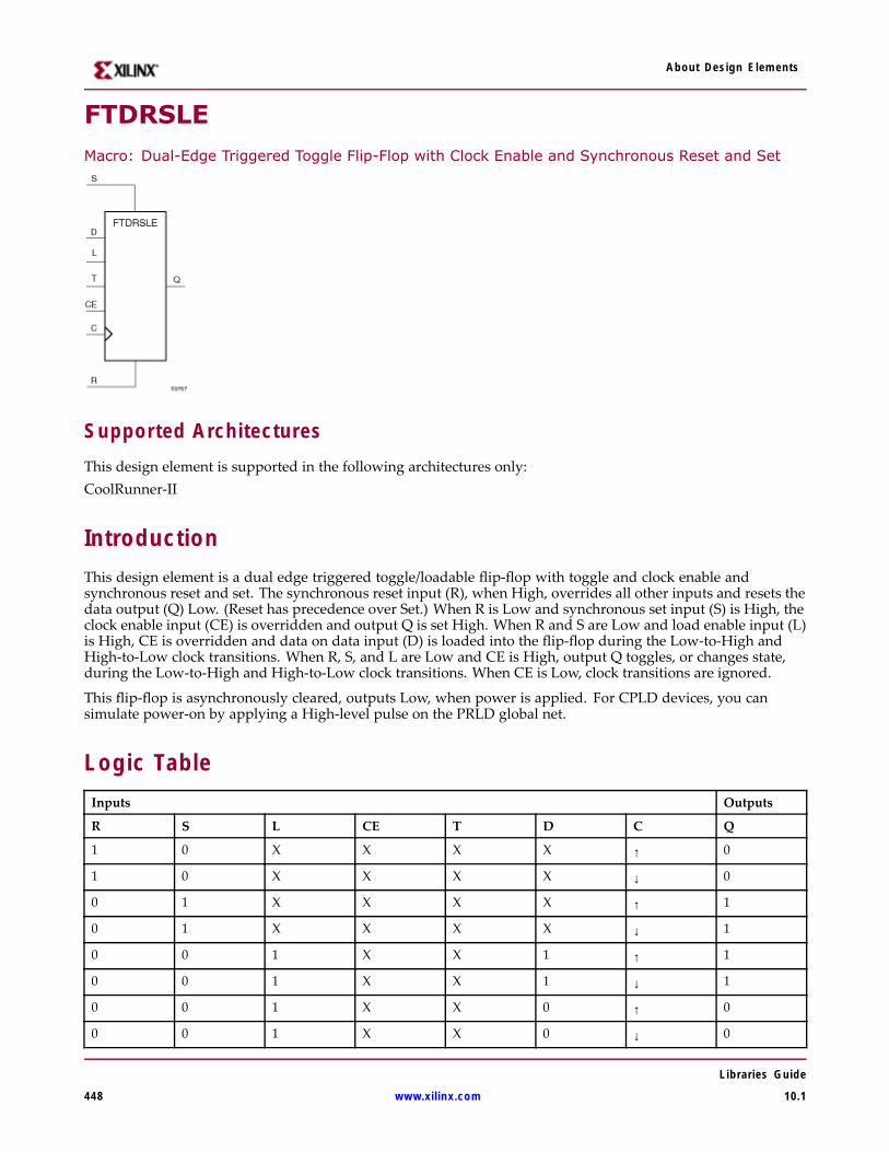
About Design Elements
FTDRSLEMacro: Dual-Edge Triggered Toggle Flip-Flop with Clock Enable and Synchronous Reset and Set
Supported ArchitecturesThis design element is supported in the following architectures only:CoolRunner-II
IntroductionThis design element is a dual edge triggered toggle/loadable flip-flop with toggle and clock enable andsynchronous reset and set. The synchronous reset input (R), when High, overrides all other inputs and resets thedata output (Q) Low. (Reset has precedence over Set.) When R is Low and synchronous set input (S) is High, theclock enable input (CE) is overridden and output Q is set High. When R and S are Low and load enable input (L)is High, CE is overridden and data on data input (D) is loaded into the flip-flop during the Low-to-High andHigh-to-Low clock transitions. When R, S, and L are Low and CE is High, output Q toggles, or changes state,during the Low-to-High and High-to-Low clock transitions. When CE is Low, clock transitions are ignored.
This flip-flop is asynchronously cleared, outputs Low, when power is applied. For CPLD devices, you cansimulate power-on by applying a High-level pulse on the PRLD global net.
Logic TableInputs Outputs
R S L CE T D C Q
1 0 X X X X ↑ 0
1 0 X X X X ↓ 0
0 1 X X X X ↑ 1
0 1 X X X X ↓ 1
0 0 1 X X 1 ↑ 1
0 0 1 X X 1 ↓ 1
0 0 1 X X 0 ↑ 0
0 0 1 X X 0 ↓ 0
Libraries Guide
448 www.xilinx.com 10.1
About Design Elements
Inputs Outputs
R S L CE T D C Q
0 0 0 0 X X X No Change
0 0 0 1 0 X X No Change
0 0 0 1 1 X ↑ Toggle
0 0 0 1 1 X ↓ Toggle
Design Entry MethodThis design element is only for use in schematics.
For More Information• See the appropriate CPLD User Guide.
• See the appropriate CPLD Data Sheets.
Libraries Guide
10.1 www.xilinx.com 449
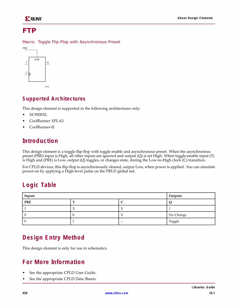
About Design Elements
FTP
Macro: Toggle Flip-Flop with Asynchronous Preset
Supported ArchitecturesThis design element is supported in the following architectures only:• XC9500XL• CoolRunner XPLA3• CoolRunner-II
IntroductionThis design element is a toggle flip-flop with toggle enable and asynchronous preset. When the asynchronouspreset (PRE) input is High, all other inputs are ignored and output (Q) is set High. When toggle-enable input (T)is High and (PRE) is Low, output (Q) toggles, or changes state, during the Low-to-High clock (C) transition.
For CPLD devices, this flip-flop is asynchronously cleared, output Low, when power is applied. You can simulatepower-on by applying a High-level pulse on the PRLD global net.
Logic TableInputs Outputs
PRE T C Q
1 X X 1
0 0 X No Change
0 1 ↑ Toggle
Design Entry MethodThis design element is only for use in schematics.
For More Information• See the appropriate CPLD User Guide.• See the appropriate CPLD Data Sheets.
Libraries Guide
450 www.xilinx.com 10.1

About Design Elements
FTPEMacro: Toggle Flip-Flop with Clock Enable and Asynchronous Preset
Supported ArchitecturesThis design element is supported in the following architectures only:• XC9500XL• CoolRunner XPLA3• CoolRunner-II
IntroductionThis design element is a toggle flip-flop with toggle and clock enable and asynchronous preset. When theasynchronous preset (PRE) input is High, all other inputs are ignored and output (Q) is set High. When thetoggle enable input (T) is High, clock enable (CE) is High, and (PRE) is Low, output (Q) toggles, or changes state,during the Low-to-High clock transition. When (CE) is Low, clock transitions are ignored.
For CPLD devices, this flip-flop is asynchronously cleared, output Low, when power is applied. You can simulatepower-on by applying a High-level pulse on the PRLD global net.
Logic TableInputs Outputs
PRE CE T C Q
1 X X X 1
0 0 X X No Change
0 1 0 X No Change
0 1 1 ↑ Toggle
Design Entry MethodThis design element is only for use in schematics.
For More Information• See the appropriate CPLD User Guide.• See the appropriate CPLD Data Sheets.
Libraries Guide
10.1 www.xilinx.com 451

About Design Elements
FTPLE
Macro: Toggle/Loadable Flip-Flop with Clock Enable and Asynchronous Preset
Supported Architectures
This design element is supported in the following architectures only:
• XC9500XL
• CoolRunner XPLA3
• CoolRunner-II
IntroductionThis design element is a toggle/loadable flip-flop with toggle and clock enable and asynchronous preset. Whenthe asynchronous preset input (PRE) is High, all other inputs are ignored and output (Q) is set High. When theload enable input (L) is High and (PRE) is Low, the clock enable (CE) is overridden and the data (D) is loadedinto the flip-flop during the Low-to-High clock transition. When L and PRE are Low and toggle-enable input(T) and (CE) are High, output (Q) toggles, or changes state, during the Low-to-High clock transition. When(CE) is Low, clock transitions are ignored.
For CPLD devices, this flip-flop is asynchronously cleared, output Low, when power is applied. You can simulatepower-on by applying a High-level pulse on the PRLD global net.
Logic TableInputs Outputs
PRE L CE T D C Q
1 X X X X X 1
0 1 X X D ↑ D
0 0 0 X X X No Change
0 0 1 0 X X No Change
0 0 1 1 X ↑ Toggle
Libraries Guide
452 www.xilinx.com 10.1

About Design Elements
Design Entry MethodThis design element is only for use in schematics.
For More Information• See the appropriate CPLD User Guide.
• See the appropriate CPLD Data Sheets.
Libraries Guide
10.1 www.xilinx.com 453
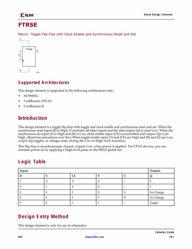
About Design Elements
FTRSE
Macro: Toggle Flip-Flop with Clock Enable and Synchronous Reset and Set
Supported Architectures
This design element is supported in the following architectures only:• XC9500XL• CoolRunner XPLA3• CoolRunner-II
IntroductionThis design element is a toggle flip-flop with toggle and clock enable and synchronous reset and set. When thesynchronous reset input (R) is High, it overrides all other inputs and the data output (Q) is reset Low. When thesynchronous set input (S) is High and (R) is Low, clock enable input (CE) is overridden and output (Q) is setHigh. (Reset has precedence over Set.) When toggle enable input (T) and (CE) are High and (R) and (S) are Low,output (Q) toggles, or changes state, during the Low-to-High clock transition.
This flip-flop is asynchronously cleared, outputs Low, when power is applied. For CPLD devices, you cansimulate power-on by applying a High-level pulse on the PRLD global net.
Logic TableInputs Outputs
R S CE T C Q
1 X X X ↑ 0
0 1 X X ↑ 1
0 0 0 X X No Change
0 0 1 0 X No Change
0 0 1 1 ↑ Toggle
Design Entry MethodThis design element is only for use in schematics.
Libraries Guide
454 www.xilinx.com 10.1

About Design Elements
For More Information• See the appropriate CPLD User Guide.
• See the appropriate CPLD Data Sheets.
Libraries Guide
10.1 www.xilinx.com 455

About Design Elements
FTRSLEMacro: Toggle/Loadable Flip-Flop with Clock Enable and Synchronous Reset and Set
Supported ArchitecturesThis design element is supported in the following architectures only:• XC9500XL• CoolRunner XPLA3• CoolRunner-II
IntroductionThis design element is a toggle/loadable flip-flop with toggle and clock enable and synchronous reset and set.The synchronous reset input (R), when High, overrides all other inputs and resets the data output (Q) Low.(Reset has precedence over Set.) When R is Low and synchronous set input (S) is High, the clock enable input(CE) is overridden and output Q is set High. When R and S are Low and load enable input (L) is High, CE isoverridden and data on data input (D) is loaded into the flip-flop during the Low-to-High clock transition. WhenR, S, and L are Low, CE is High and T is High, output Q toggles, or changes state, during the Low-to-High clocktransition. When CE is Low, clock transitions are ignored.
This flip-flop is asynchronously cleared, outputs Low, when power is applied. For CPLD devices, you cansimulate power-on by applying a High-level pulse on the PRLD global net.
Logic TableInputs Outputs
R S L CE T D C Q
1 0 X X X X ↑ 0
0 1 X X X X ↑ 1
0 0 1 X X 1 ↑ 1
0 0 1 X X 0 ↑ 0
0 0 0 0 X X X No Change
0 0 0 1 0 X X No Change
0 0 0 1 1 X ↑ Toggle
Libraries Guide
456 www.xilinx.com 10.1
About Design Elements
Design Entry MethodThis design element is only for use in schematics.
For More Information• See the appropriate CPLD User Guide.
• See the appropriate CPLD Data Sheets.
Libraries Guide
10.1 www.xilinx.com 457

About Design Elements
FTSRE
Macro: Toggle Flip-Flop with Clock Enable and Synchronous Set and Reset
Supported Architectures
This design element is supported in the following architectures only:• XC9500XL• CoolRunner XPLA3• CoolRunner-II
IntroductionThis design element is a toggle flip-flop with toggle and clock enable and synchronous set and reset. Thesynchronous set input, when High, overrides all other inputs and sets data output (Q) High. (Set has precedenceover Reset.) When synchronous reset input (R) is High and S is Low, clock enable input (CE) is overridden andoutput Q is reset Low. When toggle enable input (T) and CE are High and S and R are Low, output Q toggles, orchanges state, during the Low-to-High clock transition. When CE is Low, clock transitions are ignored.
This flip-flop is asynchronously cleared, outputs Low, when power is applied. For CPLD devices, you cansimulate power-on by applying a High-level pulse on the PRLD global net.
Logic TableInputs Outputs
S R CE T C Q
1 X X X ↑ 1
0 1 X X ↑ 0
0 0 0 X X No Change
0 0 1 0 X No Change
0 0 1 1 ↑ Toggle
Design Entry MethodThis design element is only for use in schematics.
Libraries Guide
458 www.xilinx.com 10.1

About Design Elements
For More Information• See the appropriate CPLD User Guide.
• See the appropriate CPLD Data Sheets.
Libraries Guide
10.1 www.xilinx.com 459
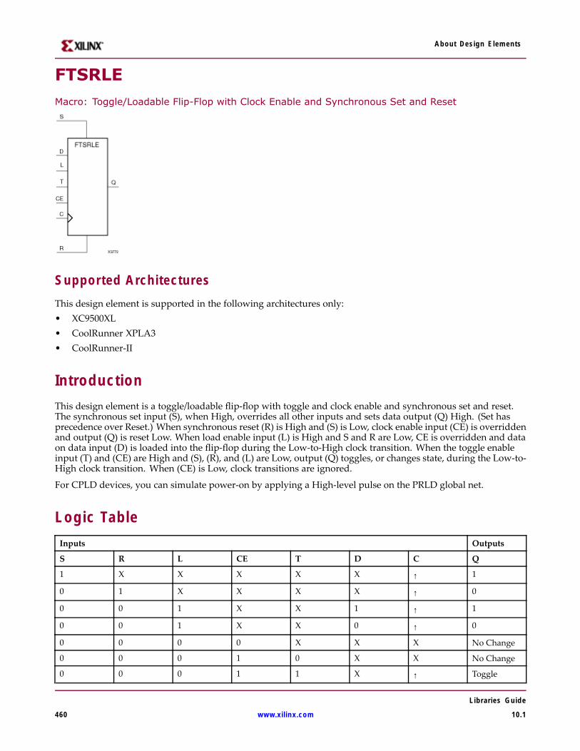
About Design Elements
FTSRLEMacro: Toggle/Loadable Flip-Flop with Clock Enable and Synchronous Set and Reset
Supported ArchitecturesThis design element is supported in the following architectures only:• XC9500XL• CoolRunner XPLA3• CoolRunner-II
IntroductionThis design element is a toggle/loadable flip-flop with toggle and clock enable and synchronous set and reset.The synchronous set input (S), when High, overrides all other inputs and sets data output (Q) High. (Set hasprecedence over Reset.) When synchronous reset (R) is High and (S) is Low, clock enable input (CE) is overriddenand output (Q) is reset Low. When load enable input (L) is High and S and R are Low, CE is overridden and dataon data input (D) is loaded into the flip-flop during the Low-to-High clock transition. When the toggle enableinput (T) and (CE) are High and (S), (R), and (L) are Low, output (Q) toggles, or changes state, during the Low-to-High clock transition. When (CE) is Low, clock transitions are ignored.
For CPLD devices, you can simulate power-on by applying a High-level pulse on the PRLD global net.
Logic TableInputs Outputs
S R L CE T D C Q
1 X X X X X ↑ 1
0 1 X X X X ↑ 0
0 0 1 X X 1 ↑ 1
0 0 1 X X 0 ↑ 0
0 0 0 0 X X X No Change
0 0 0 1 0 X X No Change
0 0 0 1 1 X ↑ Toggle
Libraries Guide
460 www.xilinx.com 10.1

About Design Elements
Design Entry MethodThis design element is only for use in schematics.
For More Information• See the appropriate CPLD User Guide.
• See the appropriate CPLD Data Sheets.
Libraries Guide
10.1 www.xilinx.com 461

About Design Elements
GND
Primitive: Ground-Connection Signal Tag
Supported Architectures
This design element is supported in the following architectures only:
• XC9500XL
• CoolRunner XPLA3
• CoolRunner-II
IntroductionThe GND signal tag, or parameter, forces a net or input function to a Low logic level. A net tied to GND cannothave any other source.
When the logic-trimming software or fitter encounters a net or input function tied to GND, it removes any logicthat is disabled by the GND signal. The GND signal is only implemented when the disabled logic cannotbe removed.
Design Entry MethodThis design element is only for use in schematics.
For More Information• See the appropriate CPLD User Guide.
• See the appropriate CPLD Data Sheets.
Libraries Guide
462 www.xilinx.com 10.1

About Design Elements
IBUF
Primitive: Input Buffer
Supported ArchitecturesThis design element is supported in the following architectures only:• XC9500XL• CoolRunner XPLA3• CoolRunner-II
IntroductionThis design element is automatically inserted (inferred) by the synthesis tool to any signal directly connectedto a top-level input or in-out port of the design. You should generally let the synthesis tool infer this buffer.However, it can be instantiated into the design if required. In order to do so, connect the input port (I) directly tothe associated top-level input or in-out port, and connect the output port (O) to the logic sourced by that port.Modify any necessary generic maps (VHDL) or named parameter value assignment (Verilog) in order to changethe default behavior of the component.
Port DescriptionsPort Direction Width Function
O Output 1 Buffer input
I Input 1 Buffer output
Design Entry MethodInstantiation Yes
Inference Recommended
Coregen and wizards No
Macro support No
This design element can be used in schematics.
In general, this element is inferred by the synthesis tool for any specified top-level input port to the design. It isgenerally not necessary to specify them in the source code however if desired, they be manually instantiated byeither copying the instantiation code from the ISE Libraries Guide HDL Template and paste it into the top-levelentity/module of your code. It is recommended to always put all I/O components on the top-level of the design tohelp facilitate hierarchical design methods. Connect the I port directly to the top-level input port of the designand the O port to the logic in which this input is to source. Specify the desired generic/defparam values inorder to configure the proper behavior of the buffer.
Libraries Guide
10.1 www.xilinx.com 463

About Design Elements
Available AttributesAttribute Type Allowed Values Default Description
IOSTANDARD String See Data Sheet "DEFAULT" Assigns an I/O standard to theelement.
VHDL Instantiation Template
Unless they already exist, copy the following two statements and paste them before the entity declaration.Library UNISIM;use UNISIM.vcomponents.all;
-- IBUF: Single-ended Input Buffer-- All devices-- Xilinx HDL Libraries Guide, version 10.1.2
IBUF_inst : IBUFgeneric map (IBUF_DELAY_VALUE => "0", -- Specify the amount of added input delay for buffer, "0"-"16" (Spartan-3E/3A only)IFD_DELAY_VALUE => "AUTO", -- Specify the amount of added delay for input register, "AUTO", "0"-"8" (Spartan-3E/3A only)IOSTANDARD => "DEFAULT")port map (O => O, -- Buffer outputI => I -- Buffer input (connect directly to top-level port));
-- End of IBUF_inst instantiation
Verilog Instantiation Template// IBUF: Single-ended Input Buffer// All devices// Xilinx HDL Libraries Guide, version 10.1.2
IBUF #(.IBUF_DELAY_VALUE("0"), // Specify the amount of added input delay for// the buffer, "0"-"16" (Spartan-3E/3A only).IFD_DELAY_VALUE("AUTO"), // Specify the amount of added delay for input// register, "AUTO", "0"-"8" (Spartan-3E/3A only).IOSTANDARD("DEFAULT") // Specify the input I/O standard)IBUF_inst (.O(O), // Buffer output.I(I) // Buffer input (connect directly to top-level port));
// End of IBUF_inst instantiation
Libraries Guide
464 www.xilinx.com 10.1

About Design Elements
For More Information• See the appropriate CPLD User Guide.
• See the appropriate CPLD Data Sheets.
Libraries Guide
10.1 www.xilinx.com 465

About Design Elements
IBUF16Macro: 16-Bit Input Buffer
Supported ArchitecturesThis design element is supported in the following architectures only:• XC9500XL• CoolRunner XPLA3• CoolRunner-II
IntroductionInput Buffers isolate the internal circuit from the signals coming into the chip. This design element is containedin input/output blocks (IOBs) and allows the specification of the particular I/O Standard to configure the I/O. Ingeneral, an this element should be used for all single-ended data input or bidirectional pins.
Design Entry MethodInstantiation Yes
Inference Recommended
Coregen and wizards No
Macro support No
This design element can be used in schematics.
In general, this element is inferred by the synthesis tool for any specified top-level input port to the design. It isgenerally not necessary to specify them in the source code however if desired, they be manually instantiated byeither copying the instantiation code from the ISE Libraries Guide HDL Template and paste it into the top-levelentity/module of your code. It is recommended to always put all I/O components on the top-level of the design tohelp facilitate hierarchical design methods. Connect the I port directly to the top-level input port of the designand the O port to the logic in which this input is to source. Specify the desired generic/defparam values inorder to configure the proper behavior of the buffer.
Available AttributesAttribute Type Allowed Values Default Description
IOSTANDARD String See Data Sheet "DEFAULT" Assigns an I/O standard to theelement.
For More Information• See the appropriate CPLD User Guide.• See the appropriate CPLD Data Sheets.
Libraries Guide
466 www.xilinx.com 10.1
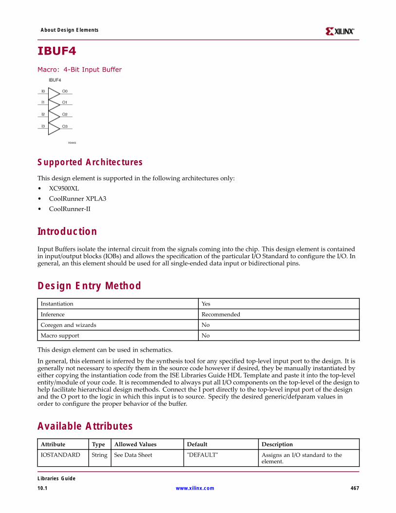
About Design Elements
IBUF4
Macro: 4-Bit Input Buffer
Supported ArchitecturesThis design element is supported in the following architectures only:• XC9500XL• CoolRunner XPLA3• CoolRunner-II
IntroductionInput Buffers isolate the internal circuit from the signals coming into the chip. This design element is containedin input/output blocks (IOBs) and allows the specification of the particular I/O Standard to configure the I/O. Ingeneral, an this element should be used for all single-ended data input or bidirectional pins.
Design Entry MethodInstantiation Yes
Inference Recommended
Coregen and wizards No
Macro support No
This design element can be used in schematics.
In general, this element is inferred by the synthesis tool for any specified top-level input port to the design. It isgenerally not necessary to specify them in the source code however if desired, they be manually instantiated byeither copying the instantiation code from the ISE Libraries Guide HDL Template and paste it into the top-levelentity/module of your code. It is recommended to always put all I/O components on the top-level of the design tohelp facilitate hierarchical design methods. Connect the I port directly to the top-level input port of the designand the O port to the logic in which this input is to source. Specify the desired generic/defparam values inorder to configure the proper behavior of the buffer.
Available AttributesAttribute Type Allowed Values Default Description
IOSTANDARD String See Data Sheet "DEFAULT" Assigns an I/O standard to theelement.
Libraries Guide
10.1 www.xilinx.com 467

About Design Elements
For More Information• See the appropriate CPLD User Guide.
• See the appropriate CPLD Data Sheets.
Libraries Guide
468 www.xilinx.com 10.1

About Design Elements
IBUF8Macro: 8-Bit Input Buffer
Supported ArchitecturesThis design element is supported in the following architectures only:• XC9500XL• CoolRunner XPLA3• CoolRunner-II
IntroductionInput Buffers isolate the internal circuit from the signals coming into the chip. This design element is containedin input/output blocks (IOBs) and allows the specification of the particular I/O Standard to configure the I/O. Ingeneral, an this element should be used for all single-ended data input or bidirectional pins.
Design Entry MethodInstantiation Yes
Inference Recommended
Coregen and wizards No
Macro support No
This design element can be used in schematics.
In general, this element is inferred by the synthesis tool for any specified top-level input port to the design. It isgenerally not necessary to specify them in the source code however if desired, they be manually instantiated byeither copying the instantiation code from the ISE Libraries Guide HDL Template and paste it into the top-levelentity/module of your code. It is recommended to always put all I/O components on the top-level of the design tohelp facilitate hierarchical design methods. Connect the I port directly to the top-level input port of the designand the O port to the logic in which this input is to source. Specify the desired generic/defparam values inorder to configure the proper behavior of the buffer.
Available AttributesAttribute Type Allowed Values Default Description
IOSTANDARD String See Data Sheet "DEFAULT" Assigns an I/O standard to theelement.
For More Information• See the appropriate CPLD User Guide.• See the appropriate CPLD Data Sheets.
Libraries Guide
10.1 www.xilinx.com 469

About Design Elements
INV
Primitive: Inverter
Supported Architectures
This design element is supported in the following architectures only:
• XC9500XL
• CoolRunner XPLA3
• CoolRunner-II
IntroductionThis design element is a single inverter that identifies signal inversions in a schematic.
Design Entry MethodThis design element is only for use in schematics.
For More Information• See the appropriate CPLD User Guide.
• See the appropriate CPLD Data Sheets.
Libraries Guide
470 www.xilinx.com 10.1

About Design Elements
INV16
Macro: 16 Inverters
Supported Architectures
This design element is supported in the following architectures only:
• XC9500XL
• CoolRunner XPLA3
• CoolRunner-II
IntroductionThis design element is a multiple inverter that identifies signal inversions in a schematic.
Design Entry MethodThis design element is only for use in schematics.
For More Information• See the appropriate CPLD User Guide.
• See the appropriate CPLD Data Sheets.
Libraries Guide
10.1 www.xilinx.com 471

About Design Elements
INV4
Macro: Four Inverters
Supported Architectures
This design element is supported in the following architectures only:
• XC9500XL
• CoolRunner XPLA3
• CoolRunner-II
IntroductionThis design element is a multiple inverter that identifies signal inversions in a schematic.
Design Entry MethodThis design element is only for use in schematics.
For More Information• See the appropriate CPLD User Guide.
• See the appropriate CPLD Data Sheets.
Libraries Guide
472 www.xilinx.com 10.1

About Design Elements
INV8
Macro: Eight Inverters
Supported Architectures
This design element is supported in the following architectures only:
• XC9500XL
• CoolRunner XPLA3
• CoolRunner-II
IntroductionThis design element is a multiple inverter that identifies signal inversions in a schematic.
Design Entry MethodThis design element is only for use in schematics.
For More Information• See the appropriate CPLD User Guide.
• See the appropriate CPLD Data Sheets.
Libraries Guide
10.1 www.xilinx.com 473

About Design Elements
IOBUFEPrimitive: Bi-Directional Buffer
Supported ArchitecturesThis design element is supported in the following architectures only:• XC9500XL• CoolRunner XPLA3• CoolRunner-II
IntroductionThis design element is a bi-directional buffer that is a composite of the IBUF and OBUFE elements. The Ooutput is X (unknown) when IO (input/output) is Z. You can also implement IOBUFEs as interconnectionsof their component elements.
Logic TableInputs Bidirectional Outputs
E I IO O
0 0 Z X
0 1 Z X
1 0 0 0
1 1 1 1
Design Entry MethodThis design element is only for use in schematics.
VHDL Instantiation TemplateUnless they already exist, copy the following two statements and paste them before the entity declaration.Library UNISIM;use UNISIM.vcomponents.all;
-- IOBUFE: Bi-Directional Buffer-- XC9500XL/CoolRunner-II/XPLA-3-- Xilinx HDL Language Template, version 10.1
IOBUFE_inst : IOBUFEport map (O => user_O,
Libraries Guide
474 www.xilinx.com 10.1

About Design Elements
IO => user_IO,I => user_I,E => user_E);
-- End of IOBUFE_inst instantiation
Verilog Instantiation Template// IOBUFE: Bi-Directional Buffer// XC9500XL/CoolRunner-II/XPLA-3// Xilinx HDL Language Template, version 10.1
IOBUFE IOBUFE_inst (.O (user_O),.IO (user_IO),.I (user_I),.E (user_E));
// End of IOBUFE_inst instantiation
For More Information• See the appropriate CPLD User Guide.
• See the appropriate CPLD Data Sheets.
Libraries Guide
10.1 www.xilinx.com 475

About Design Elements
KEEPER
Primitive: KEEPER Symbol
Supported ArchitecturesThis design element is supported in the following architectures only:• XC9500XL• CoolRunner-II
IntroductionThe design element is a weak keeper element that retains the value of the net connected to its bidirectional O pin.For example, if a logic 1 is being driven onto the net, KEEPER drives a weak/resistive 1 onto the net. If the netdriver is then 3-stated, KEEPER continues to drive a weak/resistive 1 onto the net.
Port DescriptionsName Direction Width Function
O Output 1-Bit Keeper output
Design Entry MethodInstantiation Yes
Inference Recommended
Coregen and wizards No
Macro support No
This design element can be used in schematics.
This element can be connected to a net in the following locations on a top-level schematic file:• A net connected to an input IO Marker• A net connected to both an output IO Marker and 3-statable IO element, such as an OBUFT.
VHDL Instantiation TemplateUnless they already exist, copy the following two statements and paste them before the entity declaration.Library UNISIM;use UNISIM.vcomponents.all;
Libraries Guide
476 www.xilinx.com 10.1
About Design Elements
-- KEEPER: I/O Buffer Weak Keeper-- All FPGA, CoolRunner-II-- Xilinx HDL Libraries Guide, version 10.1.2
KEEPER_inst : KEEPERport map (O => O -- Keeper output (connect directly to top-level port));
-- End of KEEPER_inst instantiation
Verilog Instantiation Template// KEEPER: I/O Buffer Weak Keeper// All FPGA, CoolRunner-II// Xilinx HDL Libraries Guide, version 10.1.2
KEEPER KEEPER_inst (.O(O) // Keeper output (connect directly to top-level port));
// End of KEEPER_inst instantiation
For More Information• See the appropriate CPLD User Guide.
• See the appropriate CPLD Data Sheets.
Libraries Guide
10.1 www.xilinx.com 477

About Design Elements
LD
Primitive: Transparent Data Latch
Supported Architectures
This design element is supported in the following architectures only:
• XC9500XL
• CoolRunner XPLA3
• CoolRunner-II
IntroductionLD is a transparent data latch. The data output (Q) of the latch reflects the data (D) input while the gate enable(G) input is High. The data on the (D) input during the High-to-Low gate transition is stored in the latch. Thedata on the (Q) output remains unchanged as long as (G) remains Low.
This latch is asynchronously cleared, outputs Low, when power is applied. For CPLD devices, you can simulatepower-on by applying a High-level pulse on the PRLD global net.
Logic TableInputs Outputs
G D Q
1 D D
0 X No Change
↓ D D
Design Entry MethodThis design element is only for use in schematics.
For More Information• See the appropriate CPLD User Guide.
• See the appropriate CPLD Data Sheets.
Libraries Guide
478 www.xilinx.com 10.1

About Design Elements
LD16
Macro: Multiple Transparent Data Latch
Supported ArchitecturesThis design element is supported in the following architectures only:• XC9500XL• CoolRunner XPLA3• CoolRunner-II
IntroductionThis design element has 16 transparent data latches with a common gate enable (G). The data output (Q) of thelatch reflects the data (D) input while the gate enable (G) input is High. The data on the (D) input during theHigh-to-Low gate transition is stored in the latch. The data on the (Q) output remains unchanged as long as(G) remains Low.
This latch is asynchronously cleared, outputs Low, when power is applied. For CPLD devices, you can simulatepower-on by applying a High-level pulse on the PRLD global net.
Logic TableInputs Outputs
G D Q
1 D D
0 X No Change
↓ Dn Dn
Design Entry MethodThis design element is only for use in schematics.
Available AttributesAttribute Type Allowed Values Default Description
INIT Binary Any 16-Bit Value All zeros Sets the initial value of Q output afterconfiguration
Libraries Guide
10.1 www.xilinx.com 479

About Design Elements
For More Information• See the appropriate CPLD User Guide.
• See the appropriate CPLD Data Sheets.
Libraries Guide
480 www.xilinx.com 10.1

About Design Elements
LD4
Macro: Multiple Transparent Data Latch
Supported Architectures
This design element is supported in the following architectures only:
• XC9500XL
• CoolRunner XPLA3
• CoolRunner-II
IntroductionThis design element has four transparent data latches with a common gate enable (G). The data output (Q) of thelatch reflects the data (D) input while the gate enable (G) input is High. The data on the (D) input during theHigh-to-Low gate transition is stored in the latch. The data on the (Q) output remains unchanged as long as(G) remains Low.
This latch is asynchronously cleared, outputs Low, when power is applied. For CPLD devices, you can simulatepower-on by applying a High-level pulse on the PRLD global net.
Logic TableInputs Outputs
G D Q
1 D D
0 X No Change
↓ Dn Dn
Design Entry MethodThis design element is only for use in schematics.
Libraries Guide
10.1 www.xilinx.com 481

About Design Elements
Available Attributes
Attribute TypeAllowedValues Default Description
INIT Binary Any 4-Bit Value All zeros Sets the initial value of Q output after configuration
For More Information• See the appropriate CPLD User Guide.
• See the appropriate CPLD Data Sheets.
Libraries Guide
482 www.xilinx.com 10.1
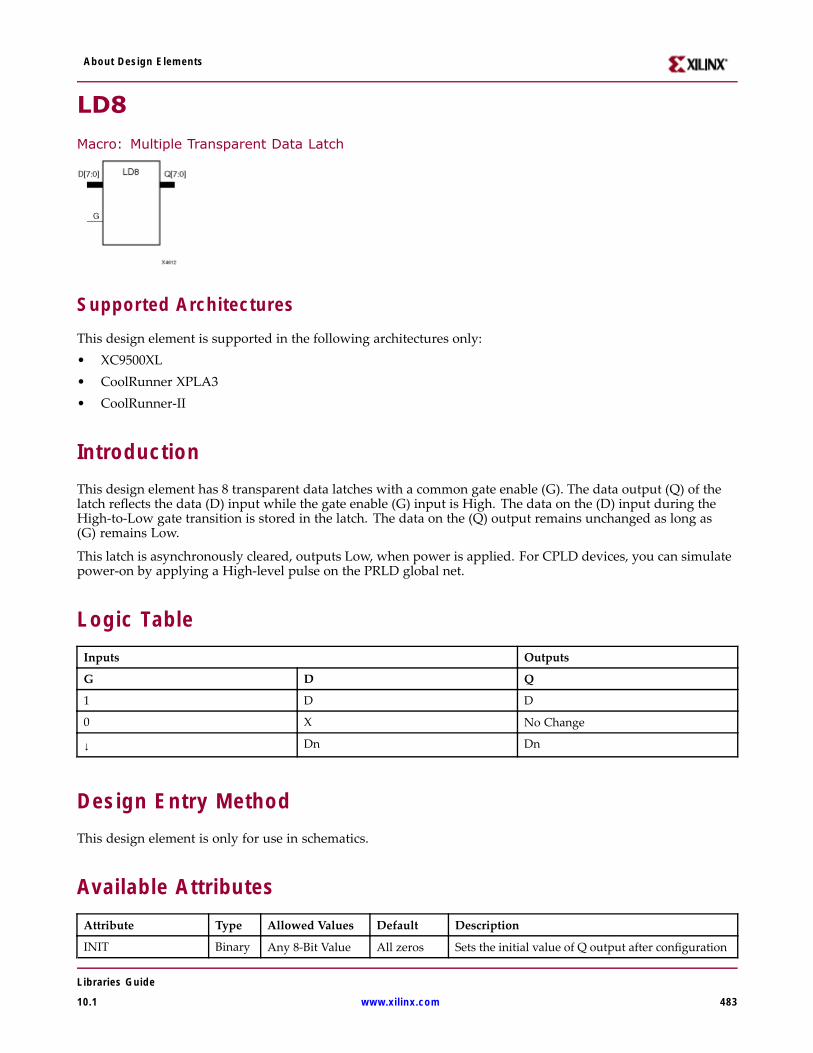
About Design Elements
LD8
Macro: Multiple Transparent Data Latch
Supported ArchitecturesThis design element is supported in the following architectures only:• XC9500XL• CoolRunner XPLA3• CoolRunner-II
IntroductionThis design element has 8 transparent data latches with a common gate enable (G). The data output (Q) of thelatch reflects the data (D) input while the gate enable (G) input is High. The data on the (D) input during theHigh-to-Low gate transition is stored in the latch. The data on the (Q) output remains unchanged as long as(G) remains Low.
This latch is asynchronously cleared, outputs Low, when power is applied. For CPLD devices, you can simulatepower-on by applying a High-level pulse on the PRLD global net.
Logic TableInputs Outputs
G D Q
1 D D
0 X No Change
↓ Dn Dn
Design Entry MethodThis design element is only for use in schematics.
Available AttributesAttribute Type Allowed Values Default Description
INIT Binary Any 8-Bit Value All zeros Sets the initial value of Q output after configuration
Libraries Guide
10.1 www.xilinx.com 483

About Design Elements
For More Information• See the appropriate CPLD User Guide.
• See the appropriate CPLD Data Sheets.
Libraries Guide
484 www.xilinx.com 10.1

About Design Elements
LDCMacro: Transparent Data Latch with Asynchronous Clear
Supported ArchitecturesThis design element is supported in the following architectures only:• XC9500XL• CoolRunner XPLA3• CoolRunner-II
IntroductionThis design element is a transparent data latch with asynchronous clear. When the asynchronous clear input(CLR) is High, it overrides the other inputs and resets the data (Q) output Low. (Q) reflects the data (D) inputwhile the gate enable (G) input is High and (CLR) is Low. The data on the (D) input during the High-to-Low gatetransition is stored in the latch. The data on the (Q) output remains unchanged as long as (G) remains low.
This latch is asynchronously cleared, outputs Low, when power is applied. For CPLD devices, you can simulatepower-on by applying a High-level pulse on the PRLD global net.
Logic TableInputs Outputs
CLR G D Q
1 X X 0
0 1 D D
0 0 X No Change
0 ↓ D D
Design Entry MethodThis design element is only for use in schematics.
Available AttributesAttribute Type Allowed Values Default Description
INIT Integer 0 or 1 0 Sets the initial value of Q output afterconfiguration.
Libraries Guide
10.1 www.xilinx.com 485

About Design Elements
For More Information• See the appropriate CPLD User Guide.
• See the appropriate CPLD Data Sheets.
Libraries Guide
486 www.xilinx.com 10.1
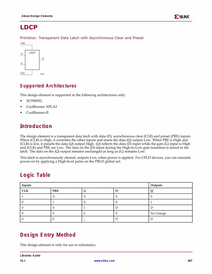
About Design Elements
LDCP
Primitive: Transparent Data Latch with Asynchronous Clear and Preset
Supported Architectures
This design element is supported in the following architectures only:
• XC9500XL
• CoolRunner XPLA3
• CoolRunner-II
IntroductionThe design element is a transparent data latch with data (D), asynchronous clear (CLR) and preset (PRE) inputs.When (CLR) is High, it overrides the other inputs and resets the data (Q) output Low. When PRE is High and(CLR) is low, it presets the data (Q) output High. (Q) reflects the data (D) input while the gate (G) input is Highand (CLR) and PRE are Low. The data on the (D) input during the High-to-Low gate transition is stored in thelatch. The data on the (Q) output remains unchanged as long as (G) remains Low.
This latch is asynchronously cleared, outputs Low, when power is applied. For CPLD devices, you can simulatepower-on by applying a High-level pulse on the PRLD global net.
Logic TableInputs Outputs
CLR PRE G D Q
1 X X X 0
0 1 X X 1
0 0 1 D D
0 0 0 X No Change
0 0 ↓ D D
Design Entry MethodThis design element is only for use in schematics.
Libraries Guide
10.1 www.xilinx.com 487

About Design Elements
Available AttributesAttribute Type Allowed Values Default Description
INIT Integer 0 or 1 0 Specifies the initial value upon power-up or theassertion of GSR for the (Q) port.
For More Information• See the appropriate CPLD User Guide.
• See the appropriate CPLD Data Sheets.
Libraries Guide
488 www.xilinx.com 10.1

About Design Elements
LDGPrimitive: Transparent Datagate Latch
Supported ArchitecturesThis design element is supported in the following architectures only:CoolRunner-II
IntroductionThis design element is a transparent DataGate latch used for gating input signals to decrease power dissipation.The data output (Q) of the latch reflects the data (D) input while the gate enable (G) input is Low. The data onthe D input during the Low-to-High gate transition is stored in the latch. The data on the Q output remainsunchanged as long as G remains High.
The D input(s) of the LDG must be connected to a device input pad(s) and must have no other fan-outs (must notbranch). The CPLD fitter maps the G input to the device’s DataGate Enable control pin (DGE). There must beno more than one DataGate Enable signal in the design. The DataGate Enable signal may be driven either bya device input pin or any on-chip logic source. The DataGate Enable signal may be reused by other ordinarylogic in the design.
This latch is asynchronously cleared, outputs Low, when power is applied. For CPLD devices, you can simulatepower-on by applying a High-level pulse on the PRLD global net.
Logic TableInputs Outputs
G D Q
0 0 0
0 1 1
1 X No Change
↑ D D
Design Entry MethodThis design element is only for use in schematics.
For More Information• See the appropriate CPLD User Guide.• See the appropriate CPLD Data Sheets.
Libraries Guide
10.1 www.xilinx.com 489

About Design Elements
LDG16Macro: 16-bit Transparent Datagate Latch
Supported ArchitecturesThis design element is supported in the following architectures only:CoolRunner-II
IntroductionThis design element has 16 transparent DataGate latches with a common gate enable (G). These latches are usedto gate input signals in order to decrease power dissipation during periods when activity on the input pins isnot of interest to the CPLD. The data output (Q) of the latch reflects the data (D) input while the gate enable(G) input is Low. The data on the D input during the Low-to-High gate transition is stored in the latch. Thedata on the Q output remains unchanged as long as G remains High.
The D input(s) of the LDG must be connected to a device input pad(s) and must have no other fan-outs (must notbranch). The CPLD fitter maps the G input to the device’s DataGate Enable control pin (DGE). There must beno more than one DataGate Enable signal in the design. The DataGate Enable signal may be driven either bya device input pin or any on-chip logic source. The DataGate Enable signal may be reused by other ordinarylogic in the design.
This latch is asynchronously cleared, outputs Low, when power is applied. For CPLD devices, you can simulatepower-on by applying a High-level pulse on the PRLD global net.
Logic TableInputs Outputs
G D Q
0 0 0
0 1 1
1 X No Change
↑ D D
Design Entry MethodThis design element is only for use in schematics.
For More Information• See the appropriate CPLD User Guide.
Libraries Guide
490 www.xilinx.com 10.1

About Design Elements
• See the appropriate CPLD Data Sheets.
Libraries Guide
10.1 www.xilinx.com 491

About Design Elements
LDG4
Macro: 4-Bit Transparent Datagate Latch
Supported ArchitecturesThis design element is supported in the following architectures only:CoolRunner-II
IntroductionThis design element has 4 transparent DataGate latches with a common gate enable (G). These latches are usedto gate input signals in order to decrease power dissipation during periods when activity on the input pins isnot of interest to the CPLD. The data output (Q) of the latch reflects the data (D) input while the gate enable(G) input is Low. The data on the D input during the Low-to-High gate transition is stored in the latch. Thedata on the Q output remains unchanged as long as G remains High.
The D input(s) of the LDG must be connected to a device input pad(s) and must have no other fan-outs (must notbranch). The CPLD fitter maps the G input to the device’s DataGate Enable control pin (DGE). There must beno more than one DataGate Enable signal in the design. The DataGate Enable signal may be driven either bya device input pin or any on-chip logic source. The DataGate Enable signal may be reused by other ordinarylogic in the design.
This latch is asynchronously cleared, outputs Low, when power is applied. For CPLD devices, you can simulatepower-on by applying a High-level pulse on the PRLD global net.
Logic TableInputs Outputs
G D Q
0 0 0
0 1 1
1 X No Change
↑ D D
Design Entry MethodThis design element is only for use in schematics.
Libraries Guide
492 www.xilinx.com 10.1

About Design Elements
For More Information• See the appropriate CPLD User Guide.
• See the appropriate CPLD Data Sheets.
Libraries Guide
10.1 www.xilinx.com 493

About Design Elements
LDG8Macro: 8-Bit Transparent Datagate Latch
Supported ArchitecturesThis design element is supported in the following architectures only:CoolRunner-II
IntroductionThis design element has 8 transparent DataGate latches with a common gate enable (G). These latches are usedto gate input signals in order to decrease power dissipation during periods when activity on the input pins isnot of interest to the CPLD. The data output (Q) of the latch reflects the data (D) input while the gate enable(G) input is Low. The data on the D input during the Low-to-High gate transition is stored in the latch. Thedata on the Q output remains unchanged as long as G remains High.
The D input(s) of the LDG must be connected to a device input pad(s) and must have no other fan-outs (must notbranch). The CPLD fitter maps the G input to the device’s DataGate Enable control pin (DGE). There must beno more than one DataGate Enable signal in the design. The DataGate Enable signal may be driven either bya device input pin or any on-chip logic source. The DataGate Enable signal may be reused by other ordinarylogic in the design.
This latch is asynchronously cleared, outputs Low, when power is applied. For CPLD devices, you can simulatepower-on by applying a High-level pulse on the PRLD global net.
Logic TableInputs Outputs
G D Q
0 0 0
0 1 1
1 X No Change
↑ D D
Design Entry MethodThis design element is only for use in schematics.
For More Information• See the appropriate CPLD User Guide.
Libraries Guide
494 www.xilinx.com 10.1

About Design Elements
• See the appropriate CPLD Data Sheets.
Libraries Guide
10.1 www.xilinx.com 495

About Design Elements
LDPMacro: Transparent Data Latch with Asynchronous Preset
Supported ArchitecturesThis design element is supported in the following architectures only:• XC9500XL• CoolRunner XPLA3• CoolRunner-II
IntroductionThis design element is a transparent data latch with asynchronous preset (PRE). When the (PRE) input is High, itoverrides the other inputs and presets the data (Q) output High. (Q) reflects the data (D) input while gate (G)input is High and (PRE) is Low. The data on the (D) input during the High-to-Low gate transition is stored in thelatch. The data on the (Q) output remains unchanged as long as (G) remains Low.
The latch is asynchronously preset, output High, when power is applied.
Logic TableInputs Outputs
PRE G D Q
1 X X 1
0 1 0 0
0 1 1 1
0 0 X No Change
0 ↓ D D
Design Entry MethodThis design element is only for use in schematics.
Available AttributesAttribute Type Allowed Values Default Description
INIT INTEGER 0 or 1 0 Specifies the initial value upon power-up or theassertion of GSR for the (Q) port.
Libraries Guide
496 www.xilinx.com 10.1

About Design Elements
For More Information• See the appropriate CPLD User Guide.
• See the appropriate CPLD Data Sheets.
Libraries Guide
10.1 www.xilinx.com 497

About Design Elements
M16_1EMacro: 16-to-1 Multiplexer with Enable
Supported ArchitecturesThis design element is supported in the following architectures only:• XC9500XL• CoolRunner XPLA3• CoolRunner-II
IntroductionThis design element is a 16-to-1 multiplexer with enable. When the enable input (E) is High, the M16_1Emultiplexer chooses one data bit from 16 sources (D15 – D0) under the control of the select inputs (S3 – S0). Theoutput (O) reflects the state of the selected input as shown in the logic table. When (E) is Low, the output is Low.
Logic TableInputs Outputs
E S3 S2 S1 S0 D15-D0 O
0 X X X X X 0
1 0 0 0 0 D0 D0
Libraries Guide
498 www.xilinx.com 10.1

About Design Elements
Inputs Outputs
E S3 S2 S1 S0 D15-D0 O
1 0 0 0 1 D1 D1
1 0 0 1 0 D2 D2
1 0 0 1 1 D3 D3...
.
.
.
.
.
.
.
.
.
.
.
.
.
.
.
.
.
.
1 1 1 0 0 D12 D12
1 1 1 0 1 D13 D13
1 1 1 1 0 D14 D14
1 1 1 1 1 D15 D15
Design Entry MethodThis design element is only for use in schematics.
For More Information• See the appropriate CPLD User Guide.
• See the appropriate CPLD Data Sheets.
Libraries Guide
10.1 www.xilinx.com 499

About Design Elements
M2_1
Macro: 2-to-1 Multiplexer
Supported Architectures
This design element is supported in the following architectures only:
• XC9500XL
• CoolRunner XPLA3
• CoolRunner-II
IntroductionThis design element chooses one data bit from two sources (D1 or D0) under the control of the select input (S0).The output (O) reflects the state of the selected data input. When Low, S0 selects D0 and when High, S0 selects D1.
Logic TableInputs Outputs
S0 D1 D0 O
1 D1 X D1
0 X D0 D0
Design Entry MethodThis design element is only for use in schematics.
For More Information• See the appropriate CPLD User Guide.
• See the appropriate CPLD Data Sheets.
Libraries Guide
500 www.xilinx.com 10.1
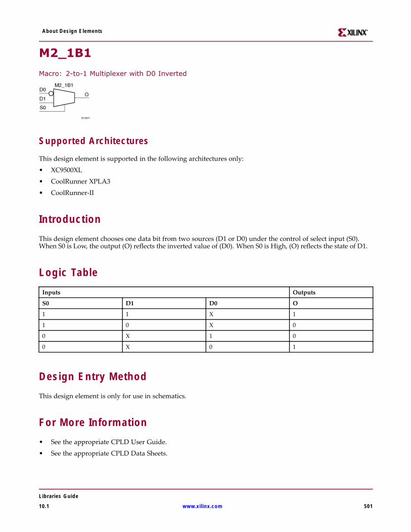
About Design Elements
M2_1B1
Macro: 2-to-1 Multiplexer with D0 Inverted
Supported Architectures
This design element is supported in the following architectures only:
• XC9500XL
• CoolRunner XPLA3
• CoolRunner-II
IntroductionThis design element chooses one data bit from two sources (D1 or D0) under the control of select input (S0).When S0 is Low, the output (O) reflects the inverted value of (D0). When S0 is High, (O) reflects the state of D1.
Logic TableInputs Outputs
S0 D1 D0 O
1 1 X 1
1 0 X 0
0 X 1 0
0 X 0 1
Design Entry MethodThis design element is only for use in schematics.
For More Information• See the appropriate CPLD User Guide.
• See the appropriate CPLD Data Sheets.
Libraries Guide
10.1 www.xilinx.com 501

About Design Elements
M2_1B2
Macro: 2-to-1 Multiplexer with D0 and D1 Inverted
Supported Architectures
This design element is supported in the following architectures only:
• XC9500XL
• CoolRunner XPLA3
• CoolRunner-II
IntroductionThis design element chooses one data bit from two sources (D1 or D0) under the control of select input (S0). WhenS0 is Low, the output (O) reflects the inverted value of D0. When S0 is High, O reflects the inverted value of D1.
Logic TableInputs Outputs
S0 D1 D0 O
1 1 X 0
1 0 X 1
0 X 1 0
0 X 0 1
Design Entry MethodThis design element is only for use in schematics.
For More Information• See the appropriate CPLD User Guide.
• See the appropriate CPLD Data Sheets.
Libraries Guide
502 www.xilinx.com 10.1

About Design Elements
M2_1E
Macro: 2-to-1 Multiplexer with Enable
Supported Architectures
This design element is supported in the following architectures only:
• XC9500XL
• CoolRunner XPLA3
• CoolRunner-II
IntroductionThis design element is a 2-to-1 multiplexer with enable. When the enable input (E) is High, the M2_1E choosesone data bit from two sources (D1 or D0) under the control of select input (S0). When Low, S0 selects D0 andwhen High, S0 selects D1. When (E) is Low, the output is Low.
Logic TableInputs Outputs
E S0 D1 D0 O
0 X X X 0
1 0 X 1 1
1 0 X 0 0
1 1 1 X 1
1 1 0 X 0
Design Entry MethodThis design element is only for use in schematics.
For More Information• See the appropriate CPLD User Guide.
• See the appropriate CPLD Data Sheets.
Libraries Guide
10.1 www.xilinx.com 503

About Design Elements
M4_1E
Macro: 4-to-1 Multiplexer with Enable
Supported ArchitecturesThis design element is supported in the following architectures only:• XC9500XL• CoolRunner XPLA3• CoolRunner-II
IntroductionThis design element is a 4-to-1 multiplexer with enable. When the enable input (E) is High, the M4_1Emultiplexerchooses one data bit from four sources (D3, D2, D1, or D0) under the control of the select inputs (S1 – S0). Theoutput (O) reflects the state of the selected input as shown in the logic table. When (E) is Low, the output is Low.
Logic TableInputs Outputs
E S1 S0 D0 D1 D2 D3 O
0 X X X X X X 0
1 0 0 D0 X X X D0
1 0 1 X D1 X X D1
1 1 0 X X D2 X D2
1 1 1 X X X D3 D3
Design Entry MethodThis design element is only for use in schematics.
For More Information• See the appropriate CPLD User Guide.• See the appropriate CPLD Data Sheets.
Libraries Guide
504 www.xilinx.com 10.1

About Design Elements
M8_1E
Macro: 8-to-1 Multiplexer with Enable
Supported Architectures
This design element is supported in the following architectures only:• XC9500XL• CoolRunner XPLA3• CoolRunner-II
IntroductionThis design element is an 8-to-1 multiplexer with enable. When the enable input (E) is High, the M8_1Emultiplexer chooses one data bit from eight sources (D7 – D0) under the control of the select inputs (S2 – S0). Theoutput (O) reflects the state of the selected input as shown in the logic table. When (E) is Low, the output is Low.
Logic TableInputs Outputs
E S2 S1 S0 D7-D0 O
0 X X X X 0
1 0 0 0 D0 D0
1 0 0 1 D1 D1
1 0 1 0 D2 D2
1 0 1 1 D3 D3
1 1 0 0 D4 D4
1 1 0 1 D5 D5
1 1 1 0 D6 D6
1 1 1 1 D7 D7
Libraries Guide
10.1 www.xilinx.com 505

About Design Elements
Design Entry MethodThis design element is only for use in schematics.
For More Information• See the appropriate CPLD User Guide.
• See the appropriate CPLD Data Sheets.
Libraries Guide
506 www.xilinx.com 10.1
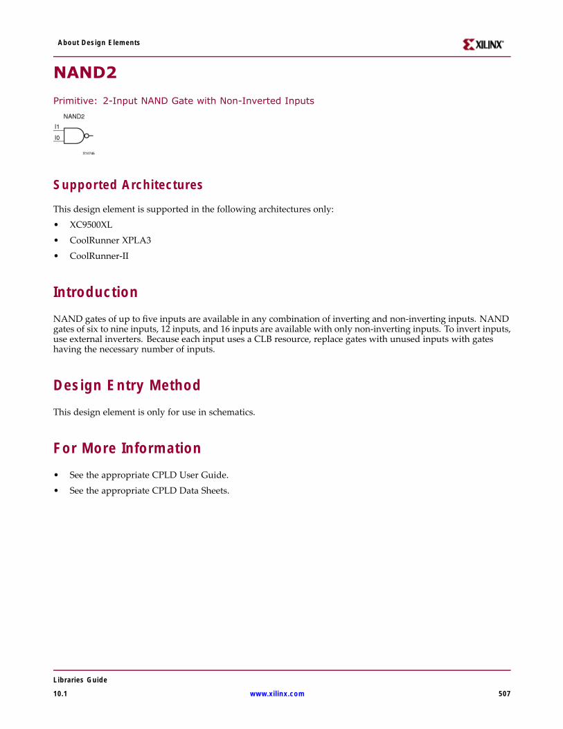
About Design Elements
NAND2
Primitive: 2-Input NAND Gate with Non-Inverted Inputs
Supported Architectures
This design element is supported in the following architectures only:
• XC9500XL
• CoolRunner XPLA3
• CoolRunner-II
IntroductionNAND gates of up to five inputs are available in any combination of inverting and non-inverting inputs. NANDgates of six to nine inputs, 12 inputs, and 16 inputs are available with only non-inverting inputs. To invert inputs,use external inverters. Because each input uses a CLB resource, replace gates with unused inputs with gateshaving the necessary number of inputs.
Design Entry MethodThis design element is only for use in schematics.
For More Information• See the appropriate CPLD User Guide.
• See the appropriate CPLD Data Sheets.
Libraries Guide
10.1 www.xilinx.com 507

About Design Elements
NAND2B1
Primitive: 2-Input NAND Gate with 1 Inverted and 1 Non-Inverted Inputs
Supported Architectures
This design element is supported in the following architectures only:
• XC9500XL
• CoolRunner XPLA3
• CoolRunner-II
IntroductionNAND gates of up to five inputs are available in any combination of inverting and non-inverting inputs. NANDgates of six to nine inputs, 12 inputs, and 16 inputs are available with only non-inverting inputs. To invert inputs,use external inverters. Because each input uses a CLB resource, replace gates with unused inputs with gateshaving the necessary number of inputs.
Design Entry MethodThis design element is only for use in schematics.
For More Information• See the appropriate CPLD User Guide.
• See the appropriate CPLD Data Sheets.
Libraries Guide
508 www.xilinx.com 10.1

About Design Elements
NAND2B2
Primitive: 2-Input NAND Gate with Inverted Inputs
Supported Architectures
This design element is supported in the following architectures only:
• XC9500XL
• CoolRunner XPLA3
• CoolRunner-II
IntroductionNAND gates of up to five inputs are available in any combination of inverting and non-inverting inputs. NANDgates of six to nine inputs, 12 inputs, and 16 inputs are available with only non-inverting inputs. To invert inputs,use external inverters. Because each input uses a CLB resource, replace gates with unused inputs with gateshaving the necessary number of inputs.
Design Entry MethodThis design element is only for use in schematics.
For More Information• See the appropriate CPLD User Guide.
• See the appropriate CPLD Data Sheets.
Libraries Guide
10.1 www.xilinx.com 509

About Design Elements
NAND3
Primitive: 3-Input NAND Gate with Non-Inverted Inputs
Supported Architectures
This design element is supported in the following architectures only:
• XC9500XL
• CoolRunner XPLA3
• CoolRunner-II
IntroductionNAND gates of up to five inputs are available in any combination of inverting and non-inverting inputs. NANDgates of six to nine inputs, 12 inputs, and 16 inputs are available with only non-inverting inputs. To invert inputs,use external inverters. Because each input uses a CLB resource, replace gates with unused inputs with gateshaving the necessary number of inputs.
Design Entry MethodThis design element is only for use in schematics.
For More Information• See the appropriate CPLD User Guide.
• See the appropriate CPLD Data Sheets.
Libraries Guide
510 www.xilinx.com 10.1

About Design Elements
NAND3B1
Primitive: 3-Input NAND Gate with 1 Inverted and 2 Non-Inverted Inputs
Supported Architectures
This design element is supported in the following architectures only:
• XC9500XL
• CoolRunner XPLA3
• CoolRunner-II
IntroductionNAND gates of up to five inputs are available in any combination of inverting and non-inverting inputs. NANDgates of six to nine inputs, 12 inputs, and 16 inputs are available with only non-inverting inputs. To invert inputs,use external inverters. Because each input uses a CLB resource, replace gates with unused inputs with gateshaving the necessary number of inputs.
Design Entry MethodThis design element is only for use in schematics.
For More Information• See the appropriate CPLD User Guide.
• See the appropriate CPLD Data Sheets.
Libraries Guide
10.1 www.xilinx.com 511
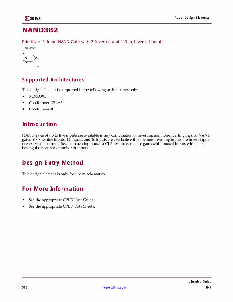
About Design Elements
NAND3B2
Primitive: 3-Input NAND Gate with 2 Inverted and 1 Non-Inverted Inputs
Supported Architectures
This design element is supported in the following architectures only:
• XC9500XL
• CoolRunner XPLA3
• CoolRunner-II
IntroductionNAND gates of up to five inputs are available in any combination of inverting and non-inverting inputs. NANDgates of six to nine inputs, 12 inputs, and 16 inputs are available with only non-inverting inputs. To invert inputs,use external inverters. Because each input uses a CLB resource, replace gates with unused inputs with gateshaving the necessary number of inputs.
Design Entry MethodThis design element is only for use in schematics.
For More Information• See the appropriate CPLD User Guide.
• See the appropriate CPLD Data Sheets.
Libraries Guide
512 www.xilinx.com 10.1

About Design Elements
NAND3B3
Primitive: 3-Input NAND Gate with Inverted Inputs
Supported Architectures
This design element is supported in the following architectures only:
• XC9500XL
• CoolRunner XPLA3
• CoolRunner-II
IntroductionNAND gates of up to five inputs are available in any combination of inverting and non-inverting inputs. NANDgates of six to nine inputs, 12 inputs, and 16 inputs are available with only non-inverting inputs. To invert inputs,use external inverters. Because each input uses a CLB resource, replace gates with unused inputs with gateshaving the necessary number of inputs.
Design Entry MethodThis design element is only for use in schematics.
For More Information• See the appropriate CPLD User Guide.
• See the appropriate CPLD Data Sheets.
Libraries Guide
10.1 www.xilinx.com 513

About Design Elements
NAND4
Primitive: 4-Input NAND Gate with Non-Inverted Inputs
Supported Architectures
This design element is supported in the following architectures only:
• XC9500XL
• CoolRunner XPLA3
• CoolRunner-II
IntroductionNAND gates of up to five inputs are available in any combination of inverting and non-inverting inputs. NANDgates of six to nine inputs, 12 inputs, and 16 inputs are available with only non-inverting inputs. To invert inputs,use external inverters. Because each input uses a CLB resource, replace gates with unused inputs with gateshaving the necessary number of inputs.
Design Entry MethodThis design element is only for use in schematics.
For More Information• See the appropriate CPLD User Guide.
• See the appropriate CPLD Data Sheets.
Libraries Guide
514 www.xilinx.com 10.1

About Design Elements
NAND4B1
Primitive: 4-Input NAND Gate with 1 Inverted and 3 Non-Inverted Inputs
Supported Architectures
This design element is supported in the following architectures only:
• XC9500XL
• CoolRunner XPLA3
• CoolRunner-II
IntroductionNAND gates of up to five inputs are available in any combination of inverting and non-inverting inputs. NANDgates of six to nine inputs, 12 inputs, and 16 inputs are available with only non-inverting inputs. To invert inputs,use external inverters. Because each input uses a CLB resource, replace gates with unused inputs with gateshaving the necessary number of inputs.
Design Entry MethodThis design element is only for use in schematics.
For More Information• See the appropriate CPLD User Guide.
• See the appropriate CPLD Data Sheets.
Libraries Guide
10.1 www.xilinx.com 515

About Design Elements
NAND4B2
Primitive: 4-Input NAND Gate with 2 Inverted and 2 Non-Inverted Inputs
Supported Architectures
This design element is supported in the following architectures only:
• XC9500XL
• CoolRunner XPLA3
• CoolRunner-II
IntroductionNAND gates of up to five inputs are available in any combination of inverting and non-inverting inputs. NANDgates of six to nine inputs, 12 inputs, and 16 inputs are available with only non-inverting inputs. To invert inputs,use external inverters. Because each input uses a CLB resource, replace gates with unused inputs with gateshaving the necessary number of inputs.
Design Entry MethodThis design element is only for use in schematics.
For More Information• See the appropriate CPLD User Guide.
• See the appropriate CPLD Data Sheets.
Libraries Guide
516 www.xilinx.com 10.1

About Design Elements
NAND4B3
Primitive: 4-Input NAND Gate with 3 Inverted and 1 Non-Inverted Inputs
Supported Architectures
This design element is supported in the following architectures only:
• XC9500XL
• CoolRunner XPLA3
• CoolRunner-II
IntroductionNAND gates of up to five inputs are available in any combination of inverting and non-inverting inputs. NANDgates of six to nine inputs, 12 inputs, and 16 inputs are available with only non-inverting inputs. To invert inputs,use external inverters. Because each input uses a CLB resource, replace gates with unused inputs with gateshaving the necessary number of inputs.
Design Entry MethodThis design element is only for use in schematics.
For More Information• See the appropriate CPLD User Guide.
• See the appropriate CPLD Data Sheets.
Libraries Guide
10.1 www.xilinx.com 517
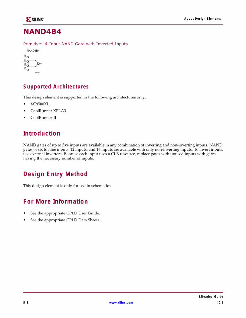
About Design Elements
NAND4B4
Primitive: 4-Input NAND Gate with Inverted Inputs
Supported Architectures
This design element is supported in the following architectures only:
• XC9500XL
• CoolRunner XPLA3
• CoolRunner-II
IntroductionNAND gates of up to five inputs are available in any combination of inverting and non-inverting inputs. NANDgates of six to nine inputs, 12 inputs, and 16 inputs are available with only non-inverting inputs. To invert inputs,use external inverters. Because each input uses a CLB resource, replace gates with unused inputs with gateshaving the necessary number of inputs.
Design Entry MethodThis design element is only for use in schematics.
For More Information• See the appropriate CPLD User Guide.
• See the appropriate CPLD Data Sheets.
Libraries Guide
518 www.xilinx.com 10.1

About Design Elements
NAND5
Primitive: 5-Input NAND Gate with Non-Inverted Inputs
Supported Architectures
This design element is supported in the following architectures only:
• XC9500XL
• CoolRunner XPLA3
• CoolRunner-II
IntroductionNAND gates of up to five inputs are available in any combination of inverting and non-inverting inputs. NANDgates of six to nine inputs, 12 inputs, and 16 inputs are available with only non-inverting inputs. To invert inputs,use external inverters. Because each input uses a CLB resource, replace gates with unused inputs with gateshaving the necessary number of inputs.
Design Entry MethodThis design element is only for use in schematics.
For More Information• See the appropriate CPLD User Guide.
• See the appropriate CPLD Data Sheets.
Libraries Guide
10.1 www.xilinx.com 519
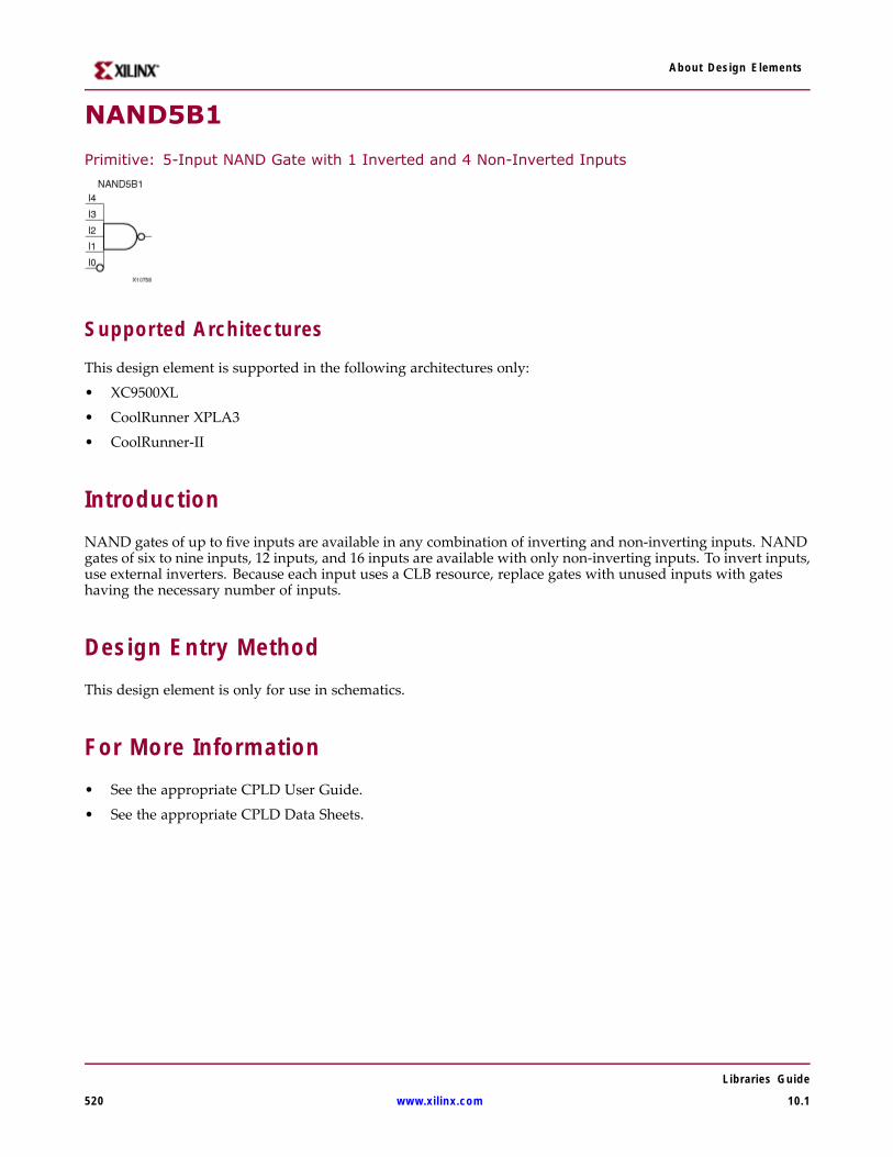
About Design Elements
NAND5B1
Primitive: 5-Input NAND Gate with 1 Inverted and 4 Non-Inverted Inputs
Supported Architectures
This design element is supported in the following architectures only:
• XC9500XL
• CoolRunner XPLA3
• CoolRunner-II
IntroductionNAND gates of up to five inputs are available in any combination of inverting and non-inverting inputs. NANDgates of six to nine inputs, 12 inputs, and 16 inputs are available with only non-inverting inputs. To invert inputs,use external inverters. Because each input uses a CLB resource, replace gates with unused inputs with gateshaving the necessary number of inputs.
Design Entry MethodThis design element is only for use in schematics.
For More Information• See the appropriate CPLD User Guide.
• See the appropriate CPLD Data Sheets.
Libraries Guide
520 www.xilinx.com 10.1

About Design Elements
NAND5B2
Primitive: 5-Input NAND Gate with 2 Inverted and 3 Non-Inverted Inputs
Supported Architectures
This design element is supported in the following architectures only:
• XC9500XL
• CoolRunner XPLA3
• CoolRunner-II
IntroductionNAND gates of up to five inputs are available in any combination of inverting and non-inverting inputs. NANDgates of six to nine inputs, 12 inputs, and 16 inputs are available with only non-inverting inputs. To invert inputs,use external inverters. Because each input uses a CLB resource, replace gates with unused inputs with gateshaving the necessary number of inputs.
Design Entry MethodThis design element is only for use in schematics.
For More Information• See the appropriate CPLD User Guide.
• See the appropriate CPLD Data Sheets.
Libraries Guide
10.1 www.xilinx.com 521

About Design Elements
NAND5B3
Primitive: 5-Input NAND Gate with 3 Inverted and 2 Non-Inverted Inputs
Supported Architectures
This design element is supported in the following architectures only:
• XC9500XL
• CoolRunner XPLA3
• CoolRunner-II
IntroductionNAND gates of up to five inputs are available in any combination of inverting and non-inverting inputs. NANDgates of six to nine inputs, 12 inputs, and 16 inputs are available with only non-inverting inputs. To invert inputs,use external inverters. Because each input uses a CLB resource, replace gates with unused inputs with gateshaving the necessary number of inputs.
Design Entry MethodThis design element is only for use in schematics.
For More Information• See the appropriate CPLD User Guide.
• See the appropriate CPLD Data Sheets.
Libraries Guide
522 www.xilinx.com 10.1

About Design Elements
NAND5B4
Primitive: 5-Input NAND Gate with 4 Inverted and 1 Non-Inverted Inputs
Supported Architectures
This design element is supported in the following architectures only:
• XC9500XL
• CoolRunner XPLA3
• CoolRunner-II
IntroductionNAND gates of up to five inputs are available in any combination of inverting and non-inverting inputs. NANDgates of six to nine inputs, 12 inputs, and 16 inputs are available with only non-inverting inputs. To invert inputs,use external inverters. Because each input uses a CLB resource, replace gates with unused inputs with gateshaving the necessary number of inputs.
Design Entry MethodThis design element is only for use in schematics.
For More Information• See the appropriate CPLD User Guide.
• See the appropriate CPLD Data Sheets.
Libraries Guide
10.1 www.xilinx.com 523

About Design Elements
NAND5B5
Primitive: 5-Input NAND Gate with Inverted Inputs
Supported Architectures
This design element is supported in the following architectures only:
• XC9500XL
• CoolRunner XPLA3
• CoolRunner-II
IntroductionNAND gates of up to five inputs are available in any combination of inverting and non-inverting inputs. NANDgates of six to nine inputs, 12 inputs, and 16 inputs are available with only non-inverting inputs. To invert inputs,use external inverters. Because each input uses a CLB resource, replace gates with unused inputs with gateshaving the necessary number of inputs.
Design Entry MethodThis design element is only for use in schematics.
For More Information• See the appropriate CPLD User Guide.
• See the appropriate CPLD Data Sheets.
Libraries Guide
524 www.xilinx.com 10.1

About Design Elements
NAND6
Macro: 6-Input NAND Gate with Non-Inverted Inputs
Supported Architectures
This design element is supported in the following architectures only:
• XC9500XL
• CoolRunner XPLA3
• CoolRunner-II
IntroductionNAND gates of up to five inputs are available in any combination of inverting and non-inverting inputs. NANDgates of six to nine inputs, 12 inputs, and 16 inputs are available with only non-inverting inputs. To invert inputs,use external inverters. Because each input uses a CLB resource, replace gates with unused inputs with gateshaving the necessary number of inputs.
Design Entry MethodThis design element is only for use in schematics.
For More Information• See the appropriate CPLD User Guide.
• See the appropriate CPLD Data Sheets.
Libraries Guide
10.1 www.xilinx.com 525
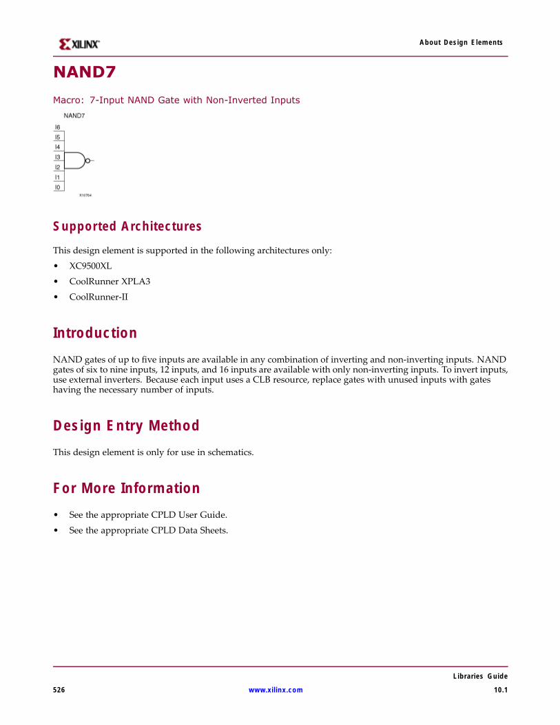
About Design Elements
NAND7
Macro: 7-Input NAND Gate with Non-Inverted Inputs
Supported Architectures
This design element is supported in the following architectures only:
• XC9500XL
• CoolRunner XPLA3
• CoolRunner-II
IntroductionNAND gates of up to five inputs are available in any combination of inverting and non-inverting inputs. NANDgates of six to nine inputs, 12 inputs, and 16 inputs are available with only non-inverting inputs. To invert inputs,use external inverters. Because each input uses a CLB resource, replace gates with unused inputs with gateshaving the necessary number of inputs.
Design Entry MethodThis design element is only for use in schematics.
For More Information• See the appropriate CPLD User Guide.
• See the appropriate CPLD Data Sheets.
Libraries Guide
526 www.xilinx.com 10.1

About Design Elements
NAND8
Macro: 8-Input NAND Gate with Non-Inverted Inputs
Supported Architectures
This design element is supported in the following architectures only:
• XC9500XL
• CoolRunner XPLA3
• CoolRunner-II
IntroductionNAND gates of up to five inputs are available in any combination of inverting and non-inverting inputs. NANDgates of six to nine inputs, 12 inputs, and 16 inputs are available with only non-inverting inputs. To invert inputs,use external inverters. Because each input uses a CLB resource, replace gates with unused inputs with gateshaving the necessary number of inputs.
Design Entry MethodThis design element is only for use in schematics.
For More Information• See the appropriate CPLD User Guide.
• See the appropriate CPLD Data Sheets.
Libraries Guide
10.1 www.xilinx.com 527
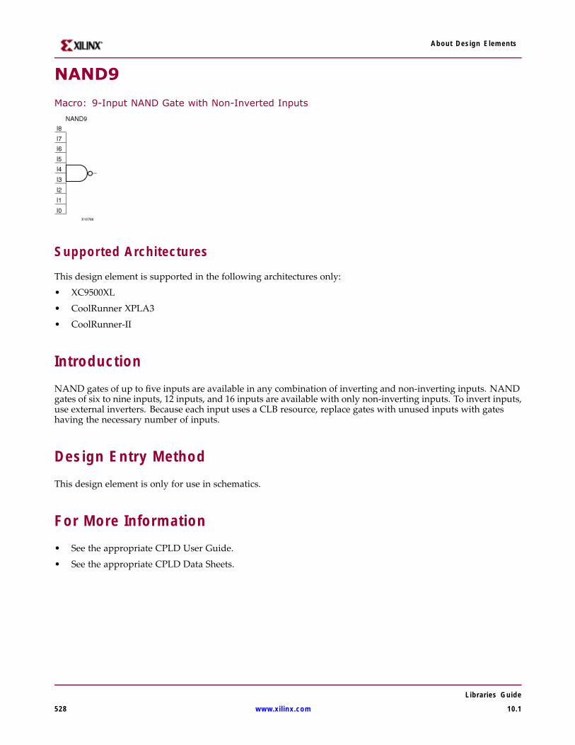
About Design Elements
NAND9
Macro: 9-Input NAND Gate with Non-Inverted Inputs
Supported Architectures
This design element is supported in the following architectures only:
• XC9500XL
• CoolRunner XPLA3
• CoolRunner-II
IntroductionNAND gates of up to five inputs are available in any combination of inverting and non-inverting inputs. NANDgates of six to nine inputs, 12 inputs, and 16 inputs are available with only non-inverting inputs. To invert inputs,use external inverters. Because each input uses a CLB resource, replace gates with unused inputs with gateshaving the necessary number of inputs.
Design Entry MethodThis design element is only for use in schematics.
For More Information• See the appropriate CPLD User Guide.
• See the appropriate CPLD Data Sheets.
Libraries Guide
528 www.xilinx.com 10.1

About Design Elements
NOR2
Primitive: 2-Input NOR Gate with Non-Inverted Inputs
Supported Architectures
This design element is supported in the following architectures only:
• XC9500XL
• CoolRunner XPLA3
• CoolRunner-II
IntroductionNOR gates of up to five inputs are available in any combination of inverting and non-inverting inputs. NORgates of six to nine inputs, 12 inputs, and 16 inputs are available only with non-inverting inputs. To invert someor all inputs, use external inverters. Because each input uses a CLB resource, replace gates with unused inputswith gates having the necessary number of inputs.
Design Entry MethodThis design element is only for use in schematics.
For More Information• See the appropriate CPLD User Guide.
• See the appropriate CPLD Data Sheets.
Libraries Guide
10.1 www.xilinx.com 529

About Design Elements
NOR2B1
Primitive: 2-Input NOR Gate with 1 Inverted and 1 Non-Inverted Inputs
Supported Architectures
This design element is supported in the following architectures only:
• XC9500XL
• CoolRunner XPLA3
• CoolRunner-II
IntroductionNOR gates of up to five inputs are available in any combination of inverting and non-inverting inputs. NORgates of six to nine inputs, 12 inputs, and 16 inputs are available only with non-inverting inputs. To invert someor all inputs, use external inverters. Because each input uses a CLB resource, replace gates with unused inputswith gates having the necessary number of inputs.
Design Entry MethodThis design element is only for use in schematics.
For More Information• See the appropriate CPLD User Guide.
• See the appropriate CPLD Data Sheets.
Libraries Guide
530 www.xilinx.com 10.1

About Design Elements
NOR2B2
Primitive: 2-Input NOR Gate with Inverted Inputs
Supported Architectures
This design element is supported in the following architectures only:
• XC9500XL
• CoolRunner XPLA3
• CoolRunner-II
IntroductionNOR gates of up to five inputs are available in any combination of inverting and non-inverting inputs. NORgates of six to nine inputs, 12 inputs, and 16 inputs are available only with non-inverting inputs. To invert someor all inputs, use external inverters. Because each input uses a CLB resource, replace gates with unused inputswith gates having the necessary number of inputs.
Design Entry MethodThis design element is only for use in schematics.
For More Information• See the appropriate CPLD User Guide.
• See the appropriate CPLD Data Sheets.
Libraries Guide
10.1 www.xilinx.com 531
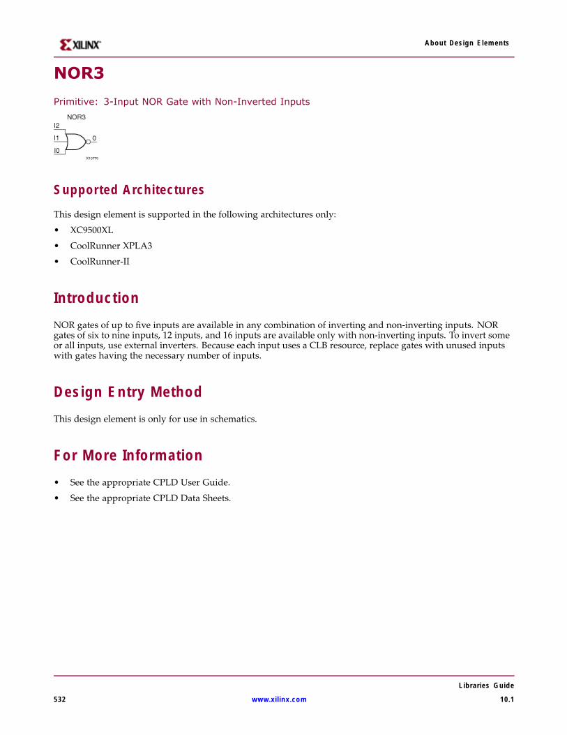
About Design Elements
NOR3
Primitive: 3-Input NOR Gate with Non-Inverted Inputs
Supported Architectures
This design element is supported in the following architectures only:
• XC9500XL
• CoolRunner XPLA3
• CoolRunner-II
IntroductionNOR gates of up to five inputs are available in any combination of inverting and non-inverting inputs. NORgates of six to nine inputs, 12 inputs, and 16 inputs are available only with non-inverting inputs. To invert someor all inputs, use external inverters. Because each input uses a CLB resource, replace gates with unused inputswith gates having the necessary number of inputs.
Design Entry MethodThis design element is only for use in schematics.
For More Information• See the appropriate CPLD User Guide.
• See the appropriate CPLD Data Sheets.
Libraries Guide
532 www.xilinx.com 10.1

About Design Elements
NOR3B1
Primitive: 3-Input NOR Gate with 1 Inverted and 2 Non-Inverted Inputs
Supported Architectures
This design element is supported in the following architectures only:
• XC9500XL
• CoolRunner XPLA3
• CoolRunner-II
IntroductionNOR gates of up to five inputs are available in any combination of inverting and non-inverting inputs. NORgates of six to nine inputs, 12 inputs, and 16 inputs are available only with non-inverting inputs. To invert someor all inputs, use external inverters. Because each input uses a CLB resource, replace gates with unused inputswith gates having the necessary number of inputs.
Design Entry MethodThis design element is only for use in schematics.
For More Information• See the appropriate CPLD User Guide.
• See the appropriate CPLD Data Sheets.
Libraries Guide
10.1 www.xilinx.com 533

About Design Elements
NOR3B2
Primitive: 3-Input NOR Gate with 2 Inverted and 1 Non-Inverted Inputs
Supported Architectures
This design element is supported in the following architectures only:
• XC9500XL
• CoolRunner XPLA3
• CoolRunner-II
IntroductionNOR gates of up to five inputs are available in any combination of inverting and non-inverting inputs. NORgates of six to nine inputs, 12 inputs, and 16 inputs are available only with non-inverting inputs. To invert someor all inputs, use external inverters. Because each input uses a CLB resource, replace gates with unused inputswith gates having the necessary number of inputs.
Design Entry MethodThis design element is only for use in schematics.
For More Information• See the appropriate CPLD User Guide.
• See the appropriate CPLD Data Sheets.
Libraries Guide
534 www.xilinx.com 10.1

About Design Elements
NOR3B3
Primitive: 3-Input NOR Gate with Inverted Inputs
Supported Architectures
This design element is supported in the following architectures only:
• XC9500XL
• CoolRunner XPLA3
• CoolRunner-II
IntroductionNOR gates of up to five inputs are available in any combination of inverting and non-inverting inputs. NORgates of six to nine inputs, 12 inputs, and 16 inputs are available only with non-inverting inputs. To invert someor all inputs, use external inverters. Because each input uses a CLB resource, replace gates with unused inputswith gates having the necessary number of inputs.
Design Entry MethodThis design element is only for use in schematics.
For More Information• See the appropriate CPLD User Guide.
• See the appropriate CPLD Data Sheets.
Libraries Guide
10.1 www.xilinx.com 535

About Design Elements
NOR4
Primitive: 4-Input NOR Gate with Non-Inverted Inputs
Supported Architectures
This design element is supported in the following architectures only:
• XC9500XL
• CoolRunner XPLA3
• CoolRunner-II
IntroductionNOR gates of up to five inputs are available in any combination of inverting and non-inverting inputs. NORgates of six to nine inputs, 12 inputs, and 16 inputs are available only with non-inverting inputs. To invert someor all inputs, use external inverters. Because each input uses a CLB resource, replace gates with unused inputswith gates having the necessary number of inputs.
Design Entry MethodThis design element is only for use in schematics.
For More Information• See the appropriate CPLD User Guide.
• See the appropriate CPLD Data Sheets.
Libraries Guide
536 www.xilinx.com 10.1

About Design Elements
NOR4B1
Primitive: 4-Input NOR Gate with 1 Inverted and 3 Non-Inverted Inputs
Supported Architectures
This design element is supported in the following architectures only:
• XC9500XL
• CoolRunner XPLA3
• CoolRunner-II
IntroductionNOR gates of up to five inputs are available in any combination of inverting and non-inverting inputs. NORgates of six to nine inputs, 12 inputs, and 16 inputs are available only with non-inverting inputs. To invert someor all inputs, use external inverters. Because each input uses a CLB resource, replace gates with unused inputswith gates having the necessary number of inputs.
Design Entry MethodThis design element is only for use in schematics.
For More Information• See the appropriate CPLD User Guide.
• See the appropriate CPLD Data Sheets.
Libraries Guide
10.1 www.xilinx.com 537

About Design Elements
NOR4B2
Primitive: 4-Input NOR Gate with 2 Inverted and 2 Non-Inverted Inputs
Supported Architectures
This design element is supported in the following architectures only:
• XC9500XL
• CoolRunner XPLA3
• CoolRunner-II
IntroductionNOR gates of up to five inputs are available in any combination of inverting and non-inverting inputs. NORgates of six to nine inputs, 12 inputs, and 16 inputs are available only with non-inverting inputs. To invert someor all inputs, use external inverters. Because each input uses a CLB resource, replace gates with unused inputswith gates having the necessary number of inputs.
Design Entry MethodThis design element is only for use in schematics.
For More Information• See the appropriate CPLD User Guide.
• See the appropriate CPLD Data Sheets.
Libraries Guide
538 www.xilinx.com 10.1

About Design Elements
NOR4B3
Primitive: 4-Input NOR Gate with 3 Inverted and 1 Non-Inverted Inputs
Supported Architectures
This design element is supported in the following architectures only:
• XC9500XL
• CoolRunner XPLA3
• CoolRunner-II
IntroductionNOR gates of up to five inputs are available in any combination of inverting and non-inverting inputs. NORgates of six to nine inputs, 12 inputs, and 16 inputs are available only with non-inverting inputs. To invert someor all inputs, use external inverters. Because each input uses a CLB resource, replace gates with unused inputswith gates having the necessary number of inputs.
Design Entry MethodThis design element is only for use in schematics.
For More Information• See the appropriate CPLD User Guide.
• See the appropriate CPLD Data Sheets.
Libraries Guide
10.1 www.xilinx.com 539
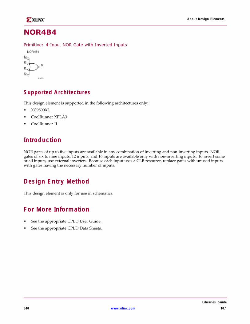
About Design Elements
NOR4B4
Primitive: 4-Input NOR Gate with Inverted Inputs
Supported Architectures
This design element is supported in the following architectures only:
• XC9500XL
• CoolRunner XPLA3
• CoolRunner-II
IntroductionNOR gates of up to five inputs are available in any combination of inverting and non-inverting inputs. NORgates of six to nine inputs, 12 inputs, and 16 inputs are available only with non-inverting inputs. To invert someor all inputs, use external inverters. Because each input uses a CLB resource, replace gates with unused inputswith gates having the necessary number of inputs.
Design Entry MethodThis design element is only for use in schematics.
For More Information• See the appropriate CPLD User Guide.
• See the appropriate CPLD Data Sheets.
Libraries Guide
540 www.xilinx.com 10.1

About Design Elements
NOR5
Primitive: 5-Input NOR Gate with Non-Inverted Inputs
Supported Architectures
This design element is supported in the following architectures only:
• XC9500XL
• CoolRunner XPLA3
• CoolRunner-II
IntroductionNOR gates of up to five inputs are available in any combination of inverting and non-inverting inputs. NORgates of six to nine inputs, 12 inputs, and 16 inputs are available only with non-inverting inputs. To invert someor all inputs, use external inverters. Because each input uses a CLB resource, replace gates with unused inputswith gates having the necessary number of inputs.
Design Entry MethodThis design element is only for use in schematics.
For More Information• See the appropriate CPLD User Guide.
• See the appropriate CPLD Data Sheets.
Libraries Guide
10.1 www.xilinx.com 541

About Design Elements
NOR5B1
Primitive: 5-Input NOR Gate with 1 Inverted and 4 Non-Inverted Inputs
Supported Architectures
This design element is supported in the following architectures only:
• XC9500XL
• CoolRunner XPLA3
• CoolRunner-II
IntroductionNOR gates of up to five inputs are available in any combination of inverting and non-inverting inputs. NORgates of six to nine inputs, 12 inputs, and 16 inputs are available only with non-inverting inputs. To invert someor all inputs, use external inverters. Because each input uses a CLB resource, replace gates with unused inputswith gates having the necessary number of inputs.
Design Entry MethodThis design element is only for use in schematics.
For More Information• See the appropriate CPLD User Guide.
• See the appropriate CPLD Data Sheets.
Libraries Guide
542 www.xilinx.com 10.1

About Design Elements
NOR5B2
Primitive: 5-Input NOR Gate with 2 Inverted and 3 Non-Inverted Inputs
Supported Architectures
This design element is supported in the following architectures only:
• XC9500XL
• CoolRunner XPLA3
• CoolRunner-II
IntroductionNOR gates of up to five inputs are available in any combination of inverting and non-inverting inputs. NORgates of six to nine inputs, 12 inputs, and 16 inputs are available only with non-inverting inputs. To invert someor all inputs, use external inverters. Because each input uses a CLB resource, replace gates with unused inputswith gates having the necessary number of inputs.
Design Entry MethodThis design element is only for use in schematics.
For More Information• See the appropriate CPLD User Guide.
• See the appropriate CPLD Data Sheets.
Libraries Guide
10.1 www.xilinx.com 543

About Design Elements
NOR5B3
Primitive: 5-Input NOR Gate with 3 Inverted and 2 Non-Inverted Inputs
Supported Architectures
This design element is supported in the following architectures only:
• XC9500XL
• CoolRunner XPLA3
• CoolRunner-II
IntroductionNOR gates of up to five inputs are available in any combination of inverting and non-inverting inputs. NORgates of six to nine inputs, 12 inputs, and 16 inputs are available only with non-inverting inputs. To invert someor all inputs, use external inverters. Because each input uses a CLB resource, replace gates with unused inputswith gates having the necessary number of inputs.
Design Entry MethodThis design element is only for use in schematics.
For More Information• See the appropriate CPLD User Guide.
• See the appropriate CPLD Data Sheets.
Libraries Guide
544 www.xilinx.com 10.1
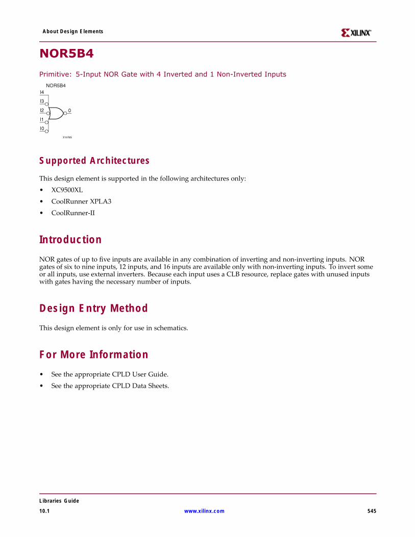
About Design Elements
NOR5B4
Primitive: 5-Input NOR Gate with 4 Inverted and 1 Non-Inverted Inputs
Supported Architectures
This design element is supported in the following architectures only:
• XC9500XL
• CoolRunner XPLA3
• CoolRunner-II
IntroductionNOR gates of up to five inputs are available in any combination of inverting and non-inverting inputs. NORgates of six to nine inputs, 12 inputs, and 16 inputs are available only with non-inverting inputs. To invert someor all inputs, use external inverters. Because each input uses a CLB resource, replace gates with unused inputswith gates having the necessary number of inputs.
Design Entry MethodThis design element is only for use in schematics.
For More Information• See the appropriate CPLD User Guide.
• See the appropriate CPLD Data Sheets.
Libraries Guide
10.1 www.xilinx.com 545

About Design Elements
NOR5B5
Primitive: 5-Input NOR Gate with Inverted Inputs
Supported Architectures
This design element is supported in the following architectures only:
• XC9500XL
• CoolRunner XPLA3
• CoolRunner-II
IntroductionNOR gates of up to five inputs are available in any combination of inverting and non-inverting inputs. NORgates of six to nine inputs, 12 inputs, and 16 inputs are available only with non-inverting inputs. To invert someor all inputs, use external inverters. Because each input uses a CLB resource, replace gates with unused inputswith gates having the necessary number of inputs.
Design Entry MethodThis design element is only for use in schematics.
For More Information• See the appropriate CPLD User Guide.
• See the appropriate CPLD Data Sheets.
Libraries Guide
546 www.xilinx.com 10.1
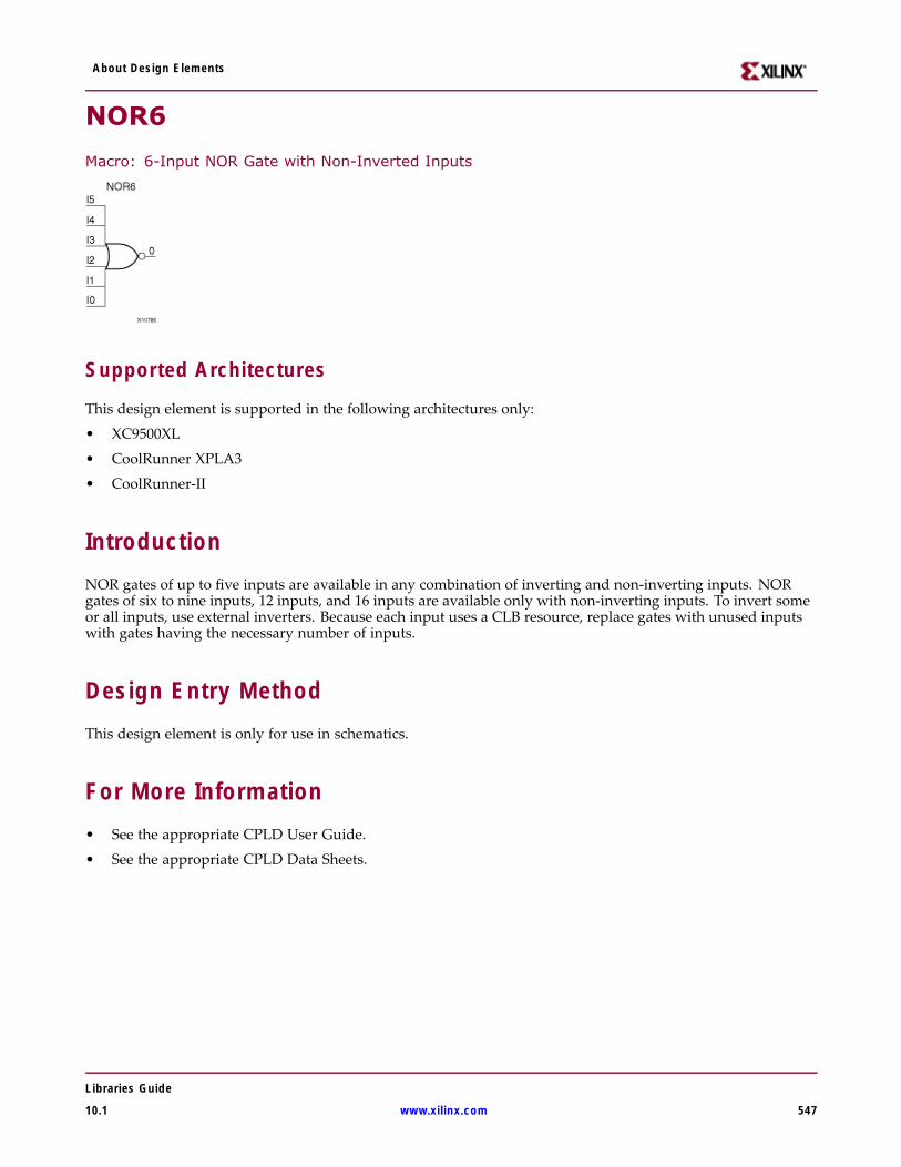
About Design Elements
NOR6
Macro: 6-Input NOR Gate with Non-Inverted Inputs
Supported Architectures
This design element is supported in the following architectures only:
• XC9500XL
• CoolRunner XPLA3
• CoolRunner-II
IntroductionNOR gates of up to five inputs are available in any combination of inverting and non-inverting inputs. NORgates of six to nine inputs, 12 inputs, and 16 inputs are available only with non-inverting inputs. To invert someor all inputs, use external inverters. Because each input uses a CLB resource, replace gates with unused inputswith gates having the necessary number of inputs.
Design Entry MethodThis design element is only for use in schematics.
For More Information• See the appropriate CPLD User Guide.
• See the appropriate CPLD Data Sheets.
Libraries Guide
10.1 www.xilinx.com 547

About Design Elements
NOR7
Macro: 7-Input NOR Gate with Non-Inverted Inputs
Supported Architectures
This design element is supported in the following architectures only:
• XC9500XL
• CoolRunner XPLA3
• CoolRunner-II
IntroductionNOR gates of up to five inputs are available in any combination of inverting and non-inverting inputs. NORgates of six to nine inputs, 12 inputs, and 16 inputs are available only with non-inverting inputs. To invert someor all inputs, use external inverters. Because each input uses a CLB resource, replace gates with unused inputswith gates having the necessary number of inputs.
Design Entry MethodThis design element is only for use in schematics.
For More Information• See the appropriate CPLD User Guide.
• See the appropriate CPLD Data Sheets.
Libraries Guide
548 www.xilinx.com 10.1

About Design Elements
NOR8
Macro: 8-Input NOR Gate with Non-Inverted Inputs
Supported Architectures
This design element is supported in the following architectures only:
• XC9500XL
• CoolRunner XPLA3
• CoolRunner-II
IntroductionNOR gates of up to five inputs are available in any combination of inverting and non-inverting inputs. NORgates of six to nine inputs, 12 inputs, and 16 inputs are available only with non-inverting inputs. To invert someor all inputs, use external inverters. Because each input uses a CLB resource, replace gates with unused inputswith gates having the necessary number of inputs.
Design Entry MethodThis design element is only for use in schematics.
For More Information• See the appropriate CPLD User Guide.
• See the appropriate CPLD Data Sheets.
Libraries Guide
10.1 www.xilinx.com 549

About Design Elements
NOR9
Macro: 9-Input NOR Gate with Non-Inverted Inputs
Supported Architectures
This design element is supported in the following architectures only:
• XC9500XL
• CoolRunner XPLA3
• CoolRunner-II
IntroductionNOR gates of up to five inputs are available in any combination of inverting and non-inverting inputs. NORgates of six to nine inputs, 12 inputs, and 16 inputs are available only with non-inverting inputs. To invert someor all inputs, use external inverters. Because each input uses a CLB resource, replace gates with unused inputswith gates having the necessary number of inputs.
Design Entry MethodThis design element is only for use in schematics.
For More Information• See the appropriate CPLD User Guide.
• See the appropriate CPLD Data Sheets.
Libraries Guide
550 www.xilinx.com 10.1

About Design Elements
OBUFPrimitive: Output Buffer
Supported ArchitecturesThis design element is supported in the following architectures only:• XC9500XL• CoolRunner XPLA3• CoolRunner-II
IntroductionThis design element is a simple output buffer used to drive output signals to the FPGA device pins that do notneed to be 3-stated (constantly driven). Either an OBUF, OBUFT, OBUFDS, or OBUFTDS must be connected toevery output port in the design.
This element isolates the internal circuit and provides drive current for signals leaving a chip. It exists ininput/output blocks (IOB). Its output (O) is connected to an OPAD or an IOPAD. The interface standard usedby this element is LVTTL. Also, this element has selectable drive and slew rates using the DRIVE and SLOWor FAST constraints. The defaults are DRIVE=12 mA and SLOW slew.
Port DescriptionsPort Direction Width Function
O Output 1 Output of OBUF to be connected directly to top-level outputport.
I Input 1 Input of OBUF. Connect to the logic driving the output port.
Design Entry MethodInstantiation Yes
Inference Recommended
Coregen and wizards No
Macro support No
This design element can be used in schematics.
Available AttributesAttribute Type Allowed Values Default Description
IOSTANDARD String See Data Sheet "DEFAULT" Assigns an I/O standard to the element.
Libraries Guide
10.1 www.xilinx.com 551

About Design Elements
VHDL Instantiation Template
Unless they already exist, copy the following two statements and paste them before the entity declaration.Library UNISIM;use UNISIM.vcomponents.all;
-- OBUF: Single-ended Output Buffer-- All devices-- Xilinx HDL Libraries Guide, version 10.1.2
OBUF_inst : OBUFgeneric map (DRIVE => 12,IOSTANDARD => "DEFAULT",SLEW => "SLOW")port map (O => O, -- Buffer output (connect directly to top-level port)I => I -- Buffer input);
-- End of OBUF_inst instantiation
Verilog Instantiation Template// OBUF: Single-ended Output Buffer// All devices// Xilinx HDL Libraries Guide, version 10.1.2
OBUF #(.DRIVE(12), // Specify the output drive strength.IOSTANDARD("DEFAULT"), // Specify the output I/O standard.SLEW("SLOW") // Specify the output slew rate) OBUF_inst (.O(O), // Buffer output (connect directly to top-level port).I(I) // Buffer input);
// End of OBUF_inst instantiation
For More Information• See the appropriate CPLD User Guide.
• See the appropriate CPLD Data Sheets.
Libraries Guide
552 www.xilinx.com 10.1

About Design Elements
OBUF16
Macro: 16-Bit Output Buffer
Supported Architectures
This design element is supported in the following architectures only:
• XC9500XL
• CoolRunner XPLA3
• CoolRunner-II
IntroductionThis design element is a multiple output buffer.
This element isolates the internal circuit and provides drive current for signals leaving a chip. It exists ininput/output blocks (IOB). Its output (O) is connected to an OPAD or an IOPAD. The interface standard usedby this element is LVTTL. Also, this element has selectable drive and slew rates using the DRIVE and SLOWor FAST constraints. The defaults are DRIVE=12 mA and SLOW slew.
Design Entry MethodInstantiation Yes
Inference Recommended
Coregen and wizards No
Macro support No
This design element can be used in schematics.
Available AttributesAttribute Type Allowed Values Default Description
IOSTANDARD String See Data Sheet "DEFAULT" Assigns an I/O standard to the element.
For More Information• See the appropriate CPLD User Guide.
• See the appropriate CPLD Data Sheets.
Libraries Guide
10.1 www.xilinx.com 553
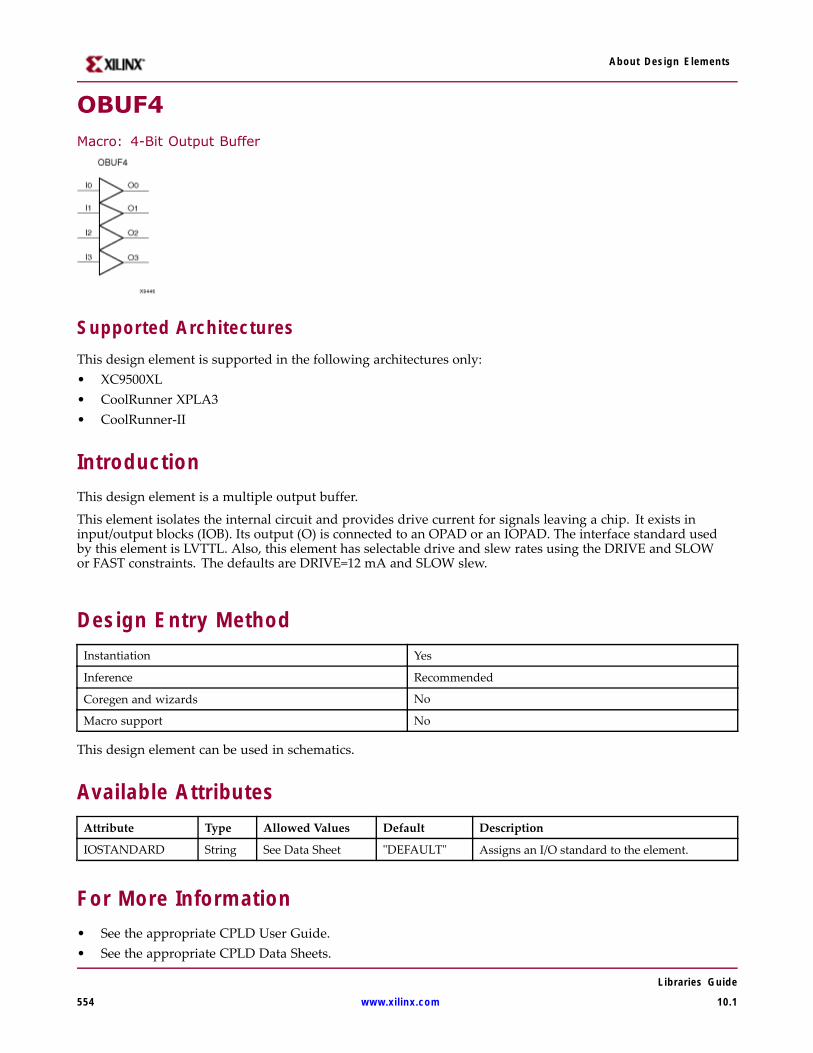
About Design Elements
OBUF4Macro: 4-Bit Output Buffer
Supported ArchitecturesThis design element is supported in the following architectures only:• XC9500XL• CoolRunner XPLA3• CoolRunner-II
IntroductionThis design element is a multiple output buffer.
This element isolates the internal circuit and provides drive current for signals leaving a chip. It exists ininput/output blocks (IOB). Its output (O) is connected to an OPAD or an IOPAD. The interface standard usedby this element is LVTTL. Also, this element has selectable drive and slew rates using the DRIVE and SLOWor FAST constraints. The defaults are DRIVE=12 mA and SLOW slew.
Design Entry MethodInstantiation Yes
Inference Recommended
Coregen and wizards No
Macro support No
This design element can be used in schematics.
Available AttributesAttribute Type Allowed Values Default Description
IOSTANDARD String See Data Sheet "DEFAULT" Assigns an I/O standard to the element.
For More Information• See the appropriate CPLD User Guide.• See the appropriate CPLD Data Sheets.
Libraries Guide
554 www.xilinx.com 10.1
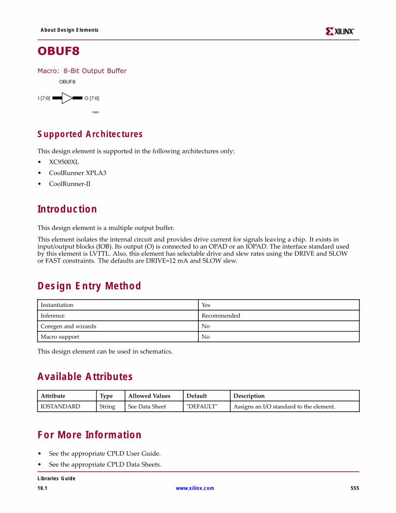
About Design Elements
OBUF8
Macro: 8-Bit Output Buffer
Supported Architectures
This design element is supported in the following architectures only:
• XC9500XL
• CoolRunner XPLA3
• CoolRunner-II
IntroductionThis design element is a multiple output buffer.
This element isolates the internal circuit and provides drive current for signals leaving a chip. It exists ininput/output blocks (IOB). Its output (O) is connected to an OPAD or an IOPAD. The interface standard usedby this element is LVTTL. Also, this element has selectable drive and slew rates using the DRIVE and SLOWor FAST constraints. The defaults are DRIVE=12 mA and SLOW slew.
Design Entry MethodInstantiation Yes
Inference Recommended
Coregen and wizards No
Macro support No
This design element can be used in schematics.
Available AttributesAttribute Type Allowed Values Default Description
IOSTANDARD String See Data Sheet "DEFAULT" Assigns an I/O standard to the element.
For More Information• See the appropriate CPLD User Guide.
• See the appropriate CPLD Data Sheets.
Libraries Guide
10.1 www.xilinx.com 555

About Design Elements
OBUFE
Macro: 3-State Output Buffer with Active-High Output Enable
Supported Architectures
This design element is supported in the following architectures only:
• XC9500XL
• CoolRunner XPLA3
• CoolRunner-II
IntroductionThis design element is a 3-state buffer with input I, output O, and active-High output enable (E).
When E is High, data on the inputs of the buffers is transferred to the corresponding outputs. When E is Low,the output is High impedance (off or Z state). This design element isolates the internal circuit and providesdrive current for signals leaving a chip. It is connected to an OPAD or an IOPAD, and its input is connected tothe internal circuit.
Logic TableInputs Outputs
E I O
0 X Z
1 1 1
1 0 0
Design Entry MethodThis design element is only for use in schematics.
For More Information• See the appropriate CPLD User Guide.
• See the appropriate CPLD Data Sheets.
Libraries Guide
556 www.xilinx.com 10.1

About Design Elements
OBUFE16
Macro: 16-Bit 3-State Output Buffer with Active-High Output Enable
Supported Architectures
This design element is supported in the following architectures only:
• XC9500XL
• CoolRunner XPLA3
• CoolRunner-II
IntroductionThis design element is a 3-state buffer with input I15-I0, output O15-O0, and active-High output enable (E).
When E is High, data on the inputs of the buffers is transferred to the corresponding outputs. When E is Low,the output is High impedance (off or Z state). This design element isolates the internal circuit and providesdrive current for signals leaving a chip. It is connected to an OPAD or an IOPAD, and its input is connected tothe internal circuit.
Logic TableInputs Outputs
E I O
0 X Z
1 1 1
1 0 0
Design Entry MethodThis design element is only for use in schematics.
For More Information• See the appropriate CPLD User Guide.
• See the appropriate CPLD Data Sheets.
Libraries Guide
10.1 www.xilinx.com 557

About Design Elements
OBUFE4Macro: 4-Bit 3-State Output Buffer with Active-High Output Enable
Supported ArchitecturesThis design element is supported in the following architectures only:• XC9500XL• CoolRunner XPLA3• CoolRunner-II
IntroductionThis design element is a 3-state buffer with input I3-I0, output O3-O0, and active-High output enable (E).
When E is High, data on the inputs of the buffers is transferred to the corresponding outputs. When E is Low,the output is High impedance (off or Z state). This design element isolates the internal circuit and providesdrive current for signals leaving a chip. It is connected to an OPAD or an IOPAD, and its input is connected tothe internal circuit.
Logic TableInputs Outputs
E I O
0 X Z
1 1 1
1 0 0
Design Entry MethodThis design element is only for use in schematics.
For More Information• See the appropriate CPLD User Guide.• See the appropriate CPLD Data Sheets.
Libraries Guide
558 www.xilinx.com 10.1

About Design Elements
OBUFE8
Macro: 8-Bit 3-State Output Buffer with Active-High Output Enable
Supported Architectures
This design element is supported in the following architectures only:
• XC9500XL
• CoolRunner XPLA3
• CoolRunner-II
IntroductionThis design element is a 3-state buffer with input I7-I0, output O7-O0, and active-High output enable (E).
When E is High, data on the inputs of the buffers is transferred to the corresponding outputs. When E is Low,the output is High impedance (off or Z state). This design element isolates the internal circuit and providesdrive current for signals leaving a chip. It is connected to an OPAD or an IOPAD, and its input is connected tothe internal circuit.
Logic TableInputs Outputs
E I O
0 X Z
1 1 1
1 0 0
Design Entry MethodThis design element is only for use in schematics.
For More Information• See the appropriate CPLD User Guide.
• See the appropriate CPLD Data Sheets.
Libraries Guide
10.1 www.xilinx.com 559

About Design Elements
OBUFTPrimitive: 3-State Output Buffer with Active Low Output Enable
Supported ArchitecturesThis design element is supported in the following architectures only:• XC9500XL• CoolRunner XPLA3• CoolRunner-II
IntroductionThis design element is a single, 3-state output buffer with input I, output O, and active-Low output enables (T).This element uses the LVTTL standard and has selectable drive and slew rates using the DRIVE and SLOW orFAST constraints. The defaults are DRIVE=12 mA and SLOW slew.
When T is Low, data on the inputs of the buffers is transferred to the corresponding outputs. When T is High, theoutput is high impedance (off or Z state). OBUFTs are generally used when a single-ended output is neededwith a 3-state capability, such as the case when building bidirectional I/O.
Logic TableInputs Outputs
T I O
1 X Z
0 I F
Port DescriptionsPort Direction Width Function
O Output 1 Buffer output (connect directly to top-level port)
I Input 1 Buffer input
T Input 1 3-state enable input
Design Entry MethodInstantiation Yes
Inference Recommended
Libraries Guide
560 www.xilinx.com 10.1

About Design Elements
Coregen and wizards No
Macro support No
This design element can be used in schematics.
Available AttributesAttribute Type Allowed Values Default Description
IOSTANDARD String See Data Sheet "DEFAULT" Assigns an I/O standard to the element.
VHDL Instantiation TemplateUnless they already exist, copy the following two statements and paste them before the entity declaration.Library UNISIM;use UNISIM.vcomponents.all;
-- OBUFT: Single-ended 3-state Output Buffer-- All devices-- Xilinx HDL Libraries Guide, version 10.1.2
OBUFT_inst : OBUFTgeneric map (DRIVE => 12,IOSTANDARD => "DEFAULT",SLEW => "SLOW")port map (O => O, -- Buffer output (connect directly to top-level port)I => I, -- Buffer inputT => T -- 3-state enable input);
-- End of OBUFT_inst instantiation
Verilog Instantiation Template// OBUFT: Single-ended 3-state Output Buffer// All devices// Xilinx HDL Libraries Guide, version 10.1.2
OBUFT #(.DRIVE(12), // Specify the output drive strength.IOSTANDARD("DEFAULT"), // Specify the output I/O standard.SLEW("SLOW") // Specify the output slew rate) OBUFT_inst (.O(O), // Buffer output (connect directly to top-level port).I(I), // Buffer input.T(T) // 3-state enable input);
// End of OBUFT_inst instantiation
For More Information• See the appropriate CPLD User Guide.• See the appropriate CPLD Data Sheets.
Libraries Guide
10.1 www.xilinx.com 561

About Design Elements
OBUFT16Macro: 16-Bit 3-State Output Buffer with Active Low Output Enable
Supported ArchitecturesThis design element is supported in the following architectures only:• XC9500XL• CoolRunner XPLA3• CoolRunner-II
IntroductionThis design element is a multiple, 3-state output buffer with input I, output O, and active-Low output enables(T). This element uses the LVTTL standard and has selectable drive and slew rates using the DRIVE and SLOWor FAST constraints. The defaults are DRIVE=12 mA and SLOW slew.
When T is Low, data on the inputs of the buffers is transferred to the corresponding outputs. When T is High, theoutput is high impedance (off or Z state). OBUFTs are generally used when a single-ended output is neededwith a 3-state capability, such as the case when building bidirectional I/O.
Logic TableInputs Outputs
T I O
1 X Z
0 I F
Design Entry MethodThis design element is only for use in schematics.
Available AttributesAttribute Type Allowed Values Default Description
IOSTANDARD String See Data Sheet "DEFAULT" Assigns an I/O standard to the element.
For More Information• See the appropriate CPLD User Guide.
Libraries Guide
562 www.xilinx.com 10.1

About Design Elements
• See the appropriate CPLD Data Sheets.
Libraries Guide
10.1 www.xilinx.com 563

About Design Elements
OBUFT4Macro: 4-Bit 3-State Output Buffers with Active-Low Output Enable
Supported ArchitecturesThis design element is supported in the following architectures only:• XC9500XL• CoolRunner XPLA3• CoolRunner-II
IntroductionThis design element is a multiple, 3-state output buffer with input I, output O, and active-Low output enables(T). This element uses the LVTTL standard and has selectable drive and slew rates using the DRIVE and SLOWor FAST constraints. The defaults are DRIVE=12 mA and SLOW slew.
When T is Low, data on the inputs of the buffers is transferred to the corresponding outputs. When T is High, theoutput is high impedance (off or Z state). OBUFTs are generally used when a single-ended output is neededwith a 3-state capability, such as the case when building bidirectional I/O.
Logic TableInputs Outputs
T I O
1 X Z
0 I F
Design Entry MethodThis design element is only for use in schematics.
Available AttributesAttribute Type Allowed Values Default Description
IOSTANDARD String See Data Sheet "DEFAULT" Assigns an I/O standard to the element.
Libraries Guide
564 www.xilinx.com 10.1

About Design Elements
For More Information• See the appropriate CPLD User Guide.
• See the appropriate CPLD Data Sheets.
Libraries Guide
10.1 www.xilinx.com 565

About Design Elements
OBUFT8Macro: 8-Bit 3-State Output Buffers with Active-Low Output Enable
Supported ArchitecturesThis design element is supported in the following architectures only:• XC9500XL• CoolRunner XPLA3• CoolRunner-II
IntroductionThis design element is a multiple, 3-state output buffer with input I, output O, and active-Low output enables(T). This element uses the LVTTL standard and has selectable drive and slew rates using the DRIVE and SLOWor FAST constraints. The defaults are DRIVE=12 mA and SLOW slew.
When T is Low, data on the inputs of the buffers is transferred to the corresponding outputs. When T is High, theoutput is high impedance (off or Z state). OBUFTs are generally used when a single-ended output is neededwith a 3-state capability, such as the case when building bidirectional I/O.
Logic TableInputs Outputs
T I O
1 X Z
0 I F
Design Entry MethodThis design element is only for use in schematics.
Available AttributesAttribute Type Allowed Values Default Description
IOSTANDARD String See Data Sheet "DEFAULT" Assigns an I/O standard to the element.
For More Information• See the appropriate CPLD User Guide.
Libraries Guide
566 www.xilinx.com 10.1

About Design Elements
• See the appropriate CPLD Data Sheets.
Libraries Guide
10.1 www.xilinx.com 567

About Design Elements
OR2
Primitive: 2-Input OR Gate with Non-Inverted Inputs
Supported Architectures
This design element is supported in the following architectures only:
• XC9500XL
• CoolRunner XPLA3
• CoolRunner-II
IntroductionOR functions of up to five inputs are available in any combination of inverting and non-inverting inputs. ORfunctions of six to nine inputs, 12 inputs, and 16 inputs are available with only non-inverting inputs. To invertsome or all inputs, use external inverters. Because each input uses a CLB resource, replace functions with unusedinputs with functions having the necessary number of inputs.
Design Entry MethodThis design element is only for use in schematics.
For More Information• See the appropriate CPLD User Guide.
• See the appropriate CPLD Data Sheets.
Libraries Guide
568 www.xilinx.com 10.1

About Design Elements
OR2B1
Primitive: 2-Input OR Gate with 1 Inverted and 1 Non-Inverted Inputs
Supported Architectures
This design element is supported in the following architectures only:
• XC9500XL
• CoolRunner XPLA3
• CoolRunner-II
IntroductionOR functions of up to five inputs are available in any combination of inverting and non-inverting inputs. ORfunctions of six to nine inputs, 12 inputs, and 16 inputs are available with only non-inverting inputs. To invertsome or all inputs, use external inverters. Because each input uses a CLB resource, replace functions with unusedinputs with functions having the necessary number of inputs.
Design Entry MethodThis design element is only for use in schematics.
For More Information• See the appropriate CPLD User Guide.
• See the appropriate CPLD Data Sheets.
Libraries Guide
10.1 www.xilinx.com 569

About Design Elements
OR2B2
Primitive: 2-Input OR Gate with Inverted Inputs
Supported Architectures
This design element is supported in the following architectures only:
• XC9500XL
• CoolRunner XPLA3
• CoolRunner-II
IntroductionOR functions of up to five inputs are available in any combination of inverting and non-inverting inputs. ORfunctions of six to nine inputs, 12 inputs, and 16 inputs are available with only non-inverting inputs. To invertsome or all inputs, use external inverters. Because each input uses a CLB resource, replace functions with unusedinputs with functions having the necessary number of inputs.
Design Entry MethodThis design element is only for use in schematics.
For More Information• See the appropriate CPLD User Guide.
• See the appropriate CPLD Data Sheets.
Libraries Guide
570 www.xilinx.com 10.1

About Design Elements
OR3
Primitive: 3-Input OR Gate with Non-Inverted Inputs
Supported Architectures
This design element is supported in the following architectures only:
• XC9500XL
• CoolRunner XPLA3
• CoolRunner-II
IntroductionOR functions of up to five inputs are available in any combination of inverting and non-inverting inputs. ORfunctions of six to nine inputs, 12 inputs, and 16 inputs are available with only non-inverting inputs. To invertsome or all inputs, use external inverters. Because each input uses a CLB resource, replace functions with unusedinputs with functions having the necessary number of inputs.
Design Entry MethodThis design element is only for use in schematics.
For More Information• See the appropriate CPLD User Guide.
• See the appropriate CPLD Data Sheets.
Libraries Guide
10.1 www.xilinx.com 571

About Design Elements
OR3B1
Primitive: 3-Input OR Gate with 1 Inverted and 2 Non-Inverted Inputs
Supported Architectures
This design element is supported in the following architectures only:
• XC9500XL
• CoolRunner XPLA3
• CoolRunner-II
IntroductionOR functions of up to five inputs are available in any combination of inverting and non-inverting inputs. ORfunctions of six to nine inputs, 12 inputs, and 16 inputs are available with only non-inverting inputs. To invertsome or all inputs, use external inverters. Because each input uses a CLB resource, replace functions with unusedinputs with functions having the necessary number of inputs.
Design Entry MethodThis design element is only for use in schematics.
For More Information• See the appropriate CPLD User Guide.
• See the appropriate CPLD Data Sheets.
Libraries Guide
572 www.xilinx.com 10.1

About Design Elements
OR3B2
Primitive: 3-Input OR Gate with 2 Inverted and 1 Non-Inverted Inputs
Supported Architectures
This design element is supported in the following architectures only:
• XC9500XL
• CoolRunner XPLA3
• CoolRunner-II
IntroductionOR functions of up to five inputs are available in any combination of inverting and non-inverting inputs. ORfunctions of six to nine inputs, 12 inputs, and 16 inputs are available with only non-inverting inputs. To invertsome or all inputs, use external inverters. Because each input uses a CLB resource, replace functions with unusedinputs with functions having the necessary number of inputs.
Design Entry MethodThis design element is only for use in schematics.
For More Information• See the appropriate CPLD User Guide.
• See the appropriate CPLD Data Sheets.
Libraries Guide
10.1 www.xilinx.com 573

About Design Elements
OR3B3
Primitive: 3-Input OR Gate with Inverted Inputs
Supported Architectures
This design element is supported in the following architectures only:
• XC9500XL
• CoolRunner XPLA3
• CoolRunner-II
IntroductionOR functions of up to five inputs are available in any combination of inverting and non-inverting inputs. ORfunctions of six to nine inputs, 12 inputs, and 16 inputs are available with only non-inverting inputs. To invertsome or all inputs, use external inverters. Because each input uses a CLB resource, replace functions with unusedinputs with functions having the necessary number of inputs.
Design Entry MethodThis design element is only for use in schematics.
For More Information• See the appropriate CPLD User Guide.
• See the appropriate CPLD Data Sheets.
Libraries Guide
574 www.xilinx.com 10.1

About Design Elements
OR4
Primitive: 4-Input OR Gate with Non-Inverted Inputs
Supported Architectures
This design element is supported in the following architectures only:
• XC9500XL
• CoolRunner XPLA3
• CoolRunner-II
IntroductionOR functions of up to five inputs are available in any combination of inverting and non-inverting inputs. ORfunctions of six to nine inputs, 12 inputs, and 16 inputs are available with only non-inverting inputs. To invertsome or all inputs, use external inverters. Because each input uses a CLB resource, replace functions with unusedinputs with functions having the necessary number of inputs.
Design Entry MethodThis design element is only for use in schematics.
For More Information• See the appropriate CPLD User Guide.
• See the appropriate CPLD Data Sheets.
Libraries Guide
10.1 www.xilinx.com 575

About Design Elements
OR4B1
Primitive: 4-Input OR Gate with 1 Inverted and 3 Non-Inverted Inputs
Supported Architectures
This design element is supported in the following architectures only:
• XC9500XL
• CoolRunner XPLA3
• CoolRunner-II
IntroductionOR functions of up to five inputs are available in any combination of inverting and non-inverting inputs. ORfunctions of six to nine inputs, 12 inputs, and 16 inputs are available with only non-inverting inputs. To invertsome or all inputs, use external inverters. Because each input uses a CLB resource, replace functions with unusedinputs with functions having the necessary number of inputs.
Design Entry MethodThis design element is only for use in schematics.
For More Information• See the appropriate CPLD User Guide.
• See the appropriate CPLD Data Sheets.
Libraries Guide
576 www.xilinx.com 10.1

About Design Elements
OR4B2
Primitive: 4-Input OR Gate with 2 Inverted and 2 Non-Inverted Inputs
Supported Architectures
This design element is supported in the following architectures only:
• XC9500XL
• CoolRunner XPLA3
• CoolRunner-II
IntroductionOR functions of up to five inputs are available in any combination of inverting and non-inverting inputs. ORfunctions of six to nine inputs, 12 inputs, and 16 inputs are available with only non-inverting inputs. To invertsome or all inputs, use external inverters. Because each input uses a CLB resource, replace functions with unusedinputs with functions having the necessary number of inputs.
Design Entry MethodThis design element is only for use in schematics.
For More Information• See the appropriate CPLD User Guide.
• See the appropriate CPLD Data Sheets.
Libraries Guide
10.1 www.xilinx.com 577

About Design Elements
OR4B3
Primitive: 4-Input OR Gate with 3 Inverted and 1 Non-Inverted Inputs
Supported Architectures
This design element is supported in the following architectures only:
• XC9500XL
• CoolRunner XPLA3
• CoolRunner-II
IntroductionOR functions of up to five inputs are available in any combination of inverting and non-inverting inputs. ORfunctions of six to nine inputs, 12 inputs, and 16 inputs are available with only non-inverting inputs. To invertsome or all inputs, use external inverters. Because each input uses a CLB resource, replace functions with unusedinputs with functions having the necessary number of inputs.
Design Entry MethodThis design element is only for use in schematics.
For More Information• See the appropriate CPLD User Guide.
• See the appropriate CPLD Data Sheets.
Libraries Guide
578 www.xilinx.com 10.1
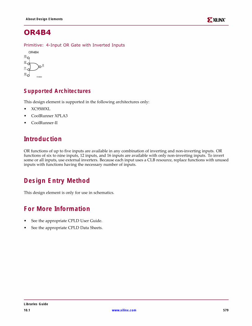
About Design Elements
OR4B4
Primitive: 4-Input OR Gate with Inverted Inputs
Supported Architectures
This design element is supported in the following architectures only:
• XC9500XL
• CoolRunner XPLA3
• CoolRunner-II
IntroductionOR functions of up to five inputs are available in any combination of inverting and non-inverting inputs. ORfunctions of six to nine inputs, 12 inputs, and 16 inputs are available with only non-inverting inputs. To invertsome or all inputs, use external inverters. Because each input uses a CLB resource, replace functions with unusedinputs with functions having the necessary number of inputs.
Design Entry MethodThis design element is only for use in schematics.
For More Information• See the appropriate CPLD User Guide.
• See the appropriate CPLD Data Sheets.
Libraries Guide
10.1 www.xilinx.com 579

About Design Elements
OR5
Primitive: 5-Input OR Gate with Non-Inverted Inputs
Supported Architectures
This design element is supported in the following architectures only:
• XC9500XL
• CoolRunner XPLA3
• CoolRunner-II
IntroductionOR functions of up to five inputs are available in any combination of inverting and non-inverting inputs. ORfunctions of six to nine inputs, 12 inputs, and 16 inputs are available with only non-inverting inputs. To invertsome or all inputs, use external inverters. Because each input uses a CLB resource, replace functions with unusedinputs with functions having the necessary number of inputs.
Design Entry MethodThis design element is only for use in schematics.
For More Information• See the appropriate CPLD User Guide.
• See the appropriate CPLD Data Sheets.
Libraries Guide
580 www.xilinx.com 10.1

About Design Elements
OR5B1
Primitive: 5-Input OR Gate with 1 Inverted and 4 Non-Inverted Inputs
Supported Architectures
This design element is supported in the following architectures only:
• XC9500XL
• CoolRunner XPLA3
• CoolRunner-II
IntroductionOR functions of up to five inputs are available in any combination of inverting and non-inverting inputs. ORfunctions of six to nine inputs, 12 inputs, and 16 inputs are available with only non-inverting inputs. To invertsome or all inputs, use external inverters. Because each input uses a CLB resource, replace functions with unusedinputs with functions having the necessary number of inputs.
Design Entry MethodThis design element is only for use in schematics.
For More Information• See the appropriate CPLD User Guide.
• See the appropriate CPLD Data Sheets.
Libraries Guide
10.1 www.xilinx.com 581
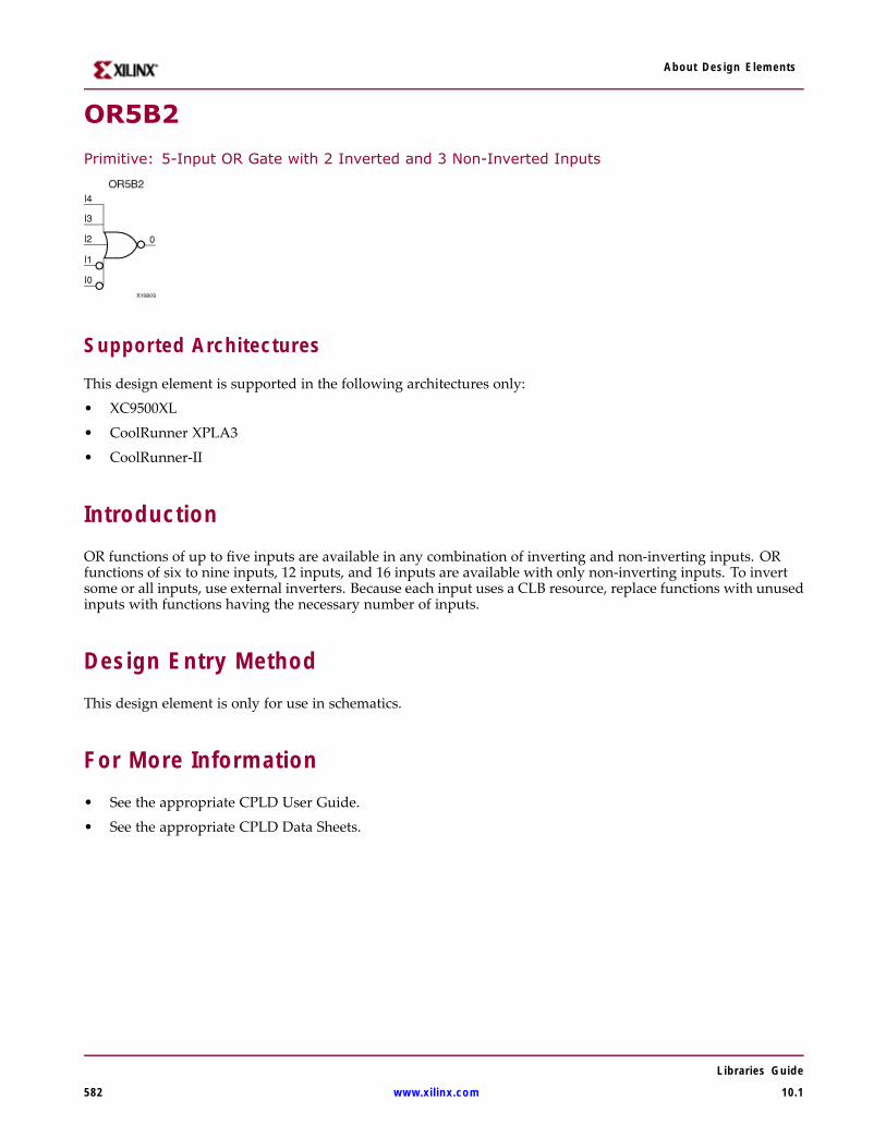
About Design Elements
OR5B2
Primitive: 5-Input OR Gate with 2 Inverted and 3 Non-Inverted Inputs
Supported Architectures
This design element is supported in the following architectures only:
• XC9500XL
• CoolRunner XPLA3
• CoolRunner-II
IntroductionOR functions of up to five inputs are available in any combination of inverting and non-inverting inputs. ORfunctions of six to nine inputs, 12 inputs, and 16 inputs are available with only non-inverting inputs. To invertsome or all inputs, use external inverters. Because each input uses a CLB resource, replace functions with unusedinputs with functions having the necessary number of inputs.
Design Entry MethodThis design element is only for use in schematics.
For More Information• See the appropriate CPLD User Guide.
• See the appropriate CPLD Data Sheets.
Libraries Guide
582 www.xilinx.com 10.1

About Design Elements
OR5B3
Primitive: 5-Input OR Gate with 3 Inverted and 2 Non-Inverted Inputs
Supported Architectures
This design element is supported in the following architectures only:
• XC9500XL
• CoolRunner XPLA3
• CoolRunner-II
IntroductionOR functions of up to five inputs are available in any combination of inverting and non-inverting inputs. ORfunctions of six to nine inputs, 12 inputs, and 16 inputs are available with only non-inverting inputs. To invertsome or all inputs, use external inverters. Because each input uses a CLB resource, replace functions with unusedinputs with functions having the necessary number of inputs.
Design Entry MethodThis design element is only for use in schematics.
For More Information• See the appropriate CPLD User Guide.
• See the appropriate CPLD Data Sheets.
Libraries Guide
10.1 www.xilinx.com 583

About Design Elements
OR5B4
Primitive: 5-Input OR Gate with 4 Inverted and 1 Non-Inverted Inputs
Supported Architectures
This design element is supported in the following architectures only:
• XC9500XL
• CoolRunner XPLA3
• CoolRunner-II
IntroductionOR functions of up to five inputs are available in any combination of inverting and non-inverting inputs. ORfunctions of six to nine inputs, 12 inputs, and 16 inputs are available with only non-inverting inputs. To invertsome or all inputs, use external inverters. Because each input uses a CLB resource, replace functions with unusedinputs with functions having the necessary number of inputs.
Design Entry MethodThis design element is only for use in schematics.
For More Information• See the appropriate CPLD User Guide.
• See the appropriate CPLD Data Sheets.
Libraries Guide
584 www.xilinx.com 10.1

About Design Elements
OR5B5
Primitive: 5-Input OR Gate with Inverted Inputs
Supported Architectures
This design element is supported in the following architectures only:
• XC9500XL
• CoolRunner XPLA3
• CoolRunner-II
IntroductionOR functions of up to five inputs are available in any combination of inverting and non-inverting inputs. ORfunctions of six to nine inputs, 12 inputs, and 16 inputs are available with only non-inverting inputs. To invertsome or all inputs, use external inverters. Because each input uses a CLB resource, replace functions with unusedinputs with functions having the necessary number of inputs.
Design Entry MethodThis design element is only for use in schematics.
For More Information• See the appropriate CPLD User Guide.
• See the appropriate CPLD Data Sheets.
Libraries Guide
10.1 www.xilinx.com 585

About Design Elements
OR6
Macro: 6-Input OR Gate with Non-Inverted Inputs
Supported Architectures
This design element is supported in the following architectures only:
• XC9500XL
• CoolRunner XPLA3
• CoolRunner-II
IntroductionOR functions of up to five inputs are available in any combination of inverting and non-inverting inputs. ORfunctions of six to nine inputs, 12 inputs, and 16 inputs are available with only non-inverting inputs. To invertsome or all inputs, use external inverters. Because each input uses a CLB resource, replace functions with unusedinputs with functions having the necessary number of inputs.
Design Entry MethodThis design element is only for use in schematics.
For More Information• See the appropriate CPLD User Guide.
• See the appropriate CPLD Data Sheets.
Libraries Guide
586 www.xilinx.com 10.1
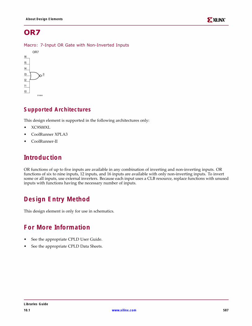
About Design Elements
OR7
Macro: 7-Input OR Gate with Non-Inverted Inputs
Supported Architectures
This design element is supported in the following architectures only:
• XC9500XL
• CoolRunner XPLA3
• CoolRunner-II
IntroductionOR functions of up to five inputs are available in any combination of inverting and non-inverting inputs. ORfunctions of six to nine inputs, 12 inputs, and 16 inputs are available with only non-inverting inputs. To invertsome or all inputs, use external inverters. Because each input uses a CLB resource, replace functions with unusedinputs with functions having the necessary number of inputs.
Design Entry MethodThis design element is only for use in schematics.
For More Information• See the appropriate CPLD User Guide.
• See the appropriate CPLD Data Sheets.
Libraries Guide
10.1 www.xilinx.com 587

About Design Elements
OR8
Macro: 8-Input OR Gate with Non-Inverted Inputs
Supported Architectures
This design element is supported in the following architectures only:
• XC9500XL
• CoolRunner XPLA3
• CoolRunner-II
IntroductionOR functions of up to five inputs are available in any combination of inverting and non-inverting inputs. ORfunctions of six to nine inputs, 12 inputs, and 16 inputs are available with only non-inverting inputs. To invertsome or all inputs, use external inverters. Because each input uses a CLB resource, replace functions with unusedinputs with functions having the necessary number of inputs.
Design Entry MethodThis design element is only for use in schematics.
For More Information• See the appropriate CPLD User Guide.
• See the appropriate CPLD Data Sheets.
Libraries Guide
588 www.xilinx.com 10.1
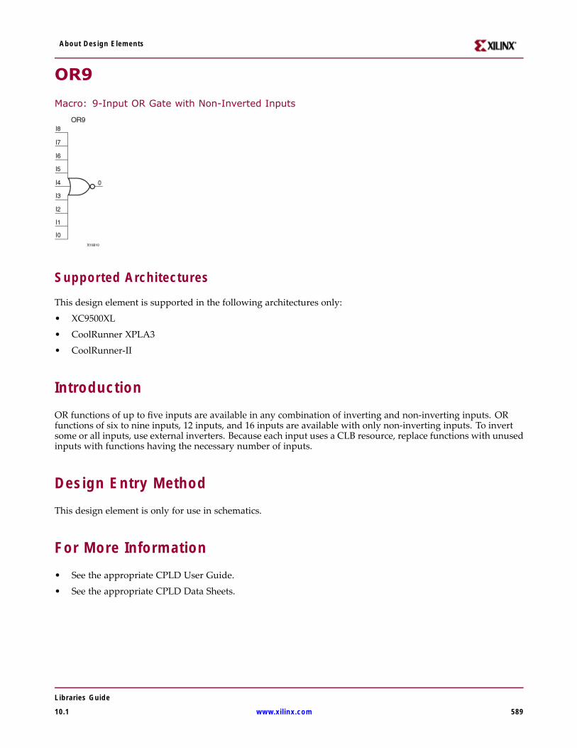
About Design Elements
OR9
Macro: 9-Input OR Gate with Non-Inverted Inputs
Supported Architectures
This design element is supported in the following architectures only:
• XC9500XL
• CoolRunner XPLA3
• CoolRunner-II
IntroductionOR functions of up to five inputs are available in any combination of inverting and non-inverting inputs. ORfunctions of six to nine inputs, 12 inputs, and 16 inputs are available with only non-inverting inputs. To invertsome or all inputs, use external inverters. Because each input uses a CLB resource, replace functions with unusedinputs with functions having the necessary number of inputs.
Design Entry MethodThis design element is only for use in schematics.
For More Information• See the appropriate CPLD User Guide.
• See the appropriate CPLD Data Sheets.
Libraries Guide
10.1 www.xilinx.com 589

About Design Elements
PULLDOWNPrimitive: Resistor to GND for Input Pads, Open-Drain, and 3-State Outputs
Supported ArchitecturesThis design element is supported in the following architectures only:• XC9500XL• CoolRunner XPLA3• CoolRunner-II
IntroductionThis resistor element is connected to input, output, or bidirectional pads to guarantee a logic Low level fornodes that might float.
Port DescriptionsPort Direction Width Function
O Output 1 Pulldown output (connect directly to top level port)
Design Entry MethodInstantiation Yes
Inference Recommended
Coregen and wizards No
Macro support No
This design element can be used in schematics.
This element can be connected to a net in the following locations on a top-level schematic file:• A net connected to an input IO Marker• A net connected to both an output IO Marker and 3-statable IO element, such as an OBUFT.
VHDL Instantiation TemplateUnless they already exist, copy the following two statements and paste them before the entity declaration.Library UNISIM;use UNISIM.vcomponents.all;
-- PULLDOWN: I/O Buffer Weak Pull-down-- All FPGA
Libraries Guide
590 www.xilinx.com 10.1
About Design Elements
-- Xilinx HDL Libraries Guide, version 10.1.2
PULLDOWN_inst : PULLDOWNport map (O => O -- Pulldown output (connect directly to top-level port));
-- End of PULLDOWN_inst instantiation
Verilog Instantiation Template// PULLDOWN: I/O Buffer Weak Pull-down// All FPGA// Xilinx HDL Libraries Guide, version 10.1.2
PULLDOWN PULLDOWN_inst (.O(O) // Pulldown output (connect directly to top-level port));
// End of PULLDOWN_inst instantiation
For More Information• See the appropriate CPLD User Guide.
• See the appropriate CPLD Data Sheets.
Libraries Guide
10.1 www.xilinx.com 591

About Design Elements
PULLUPPrimitive: Resistor to VCC for Input PADs, Open-Drain, and 3-State Outputs
Supported ArchitecturesThis design element is supported in the following architectures only:• CoolRunner XPLA3• CoolRunner-II
IntroductionThis design element allows for an input, 3-state output or bi-directional port to be driven to a weak highvalue when not being driven by an internal or external source. This element establishes a High logic level foropen-drain elements and macros when all the drivers are off.
Port DescriptionsPort Direction Width Function
O Output 1 Pullup output (connect directly to top level port)
Design Entry MethodInstantiation Yes
Inference Recommended
Coregen and wizards No
Macro support No
This design element can be used in schematics.
This element can be connected to a net in the following locations on a top-level schematic file:• A net connected to an input IO Marker• A net connected to both an output IO Marker and 3-statable IO element, such as an OBUFT.
VHDL Instantiation TemplateUnless they already exist, copy the following two statements and paste them before the entity declaration.Library UNISIM;use UNISIM.vcomponents.all;
-- PULLUP: I/O Buffer Weak Pull-up-- All FPGA, CoolRunner-II-- Xilinx HDL Libraries Guide, version 10.1.2
PULLUP_inst : PULLUP
Libraries Guide
592 www.xilinx.com 10.1
About Design Elements
port map (O => O -- Pullup output (connect directly to top-level port));
-- End of PULLUP_inst instantiation
Verilog Instantiation Template// PULLUP: I/O Buffer Weak Pull-up// All FPGA, CoolRunner-II// Xilinx HDL Libraries Guide, version 10.1.2
PULLUP PULLUP_inst (.O(O) // Pullup output (connect directly to top-level port));
// End of PULLUP_inst instantiation
For More Information• See the appropriate CPLD User Guide.
• See the appropriate CPLD Data Sheets.
Libraries Guide
10.1 www.xilinx.com 593
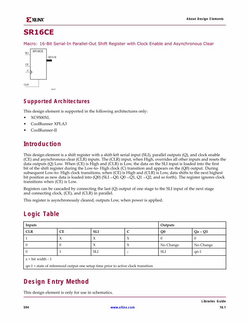
About Design Elements
SR16CEMacro: 16-Bit Serial-In Parallel-Out Shift Register with Clock Enable and Asynchronous Clear
Supported ArchitecturesThis design element is supported in the following architectures only:• XC9500XL• CoolRunner XPLA3• CoolRunner-II
IntroductionThis design element is a shift register with a shift-left serial input (SLI), parallel outputs (Q), and clock enable(CE) and asynchronous clear (CLR) inputs. The (CLR) input, when High, overrides all other inputs and resets thedata outputs (Q) Low. When (CE) is High and (CLR) is Low, the data on the SLI input is loaded into the firstbit of the shift register during the Low-to- High clock (C) transition and appears on the (Q0) output. Duringsubsequent Low-to- High clock transitions, when (CE) is High and (CLR) is Low, data shifts to the next highestbit position as new data is loaded into (Q0) (SLI→Q0, Q0→Q1, Q1→Q2, and so forth). The register ignores clocktransitions when (CE) is Low.
Registers can be cascaded by connecting the last (Q) output of one stage to the SLI input of the next stageand connecting clock, (CE), and (CLR) in parallel.
This register is asynchronously cleared, outputs Low, when power is applied.
Logic TableInputs Outputs
CLR CE SLI C Q0 Qz – Q1
1 X X X 0 0
0 0 X X No Change No Change
0 1 SLI ↑ SLI qn-1
z = bit width - 1
qn-1 = state of referenced output one setup time prior to active clock transition
Design Entry MethodThis design element is only for use in schematics.
Libraries Guide
594 www.xilinx.com 10.1
About Design Elements
For More Information• See the appropriate CPLD User Guide.
• See the appropriate CPLD Data Sheets.
Libraries Guide
10.1 www.xilinx.com 595

About Design Elements
SR16CLEMacro: 16-Bit Loadable Serial/Parallel-In Parallel-Out Shift Register with Clock Enable andAsynchronous Clear
Supported ArchitecturesThis design element is supported in the following architectures only:• XC9500XL• CoolRunner XPLA3• CoolRunner-II
IntroductionThis design element is a shift register with a shift-left serial input (SLI), parallel inputs (D), parallel outputs (Q),and three control inputs: clock enable (CE), load enable (L), and asynchronous clear (CLR) . The register ignoresclock transitions when (L) and (CE) are Low. The asynchronous (CLR), when High, overrides all other inputsand resets the data outputs (Q) Low. When (L) is High and (CLR) is Low, data on the Dn – D0 inputs is loadedinto the corresponding Qn – (Q0) bits of the register.
When (CE) is High and (L) and (CLR) are Low, data on the SLI input is loaded into the first bit of the shiftregister during the Low-to-High clock (C) transition and appears on the (Q0) output. During subsequent clocktransitions, when (CE) is High and (L) and (CLR) are Low, the data shifts to the next highest bit position as newdata is loaded into (Q)0 (for example, SLI→Q0, Q0→Q1, and Q1→Q2).
Registers can be cascaded by connecting the last (Q) output of one stage to the SLI input of the next stage andconnecting clock, (CE), (L), and (CLR) inputs in parallel.
This register is asynchronously cleared, outputs Low, when power is applied.
Logic TableInputs Outputs
CLR L CE SLI Dn – D0 C Q0 Qz – Q1
1 X X X X X 0 0
0 1 X X Dn – D0 ↑ D0 Dn
0 0 1 SLI X ↑ SLI qn-1
Libraries Guide
596 www.xilinx.com 10.1
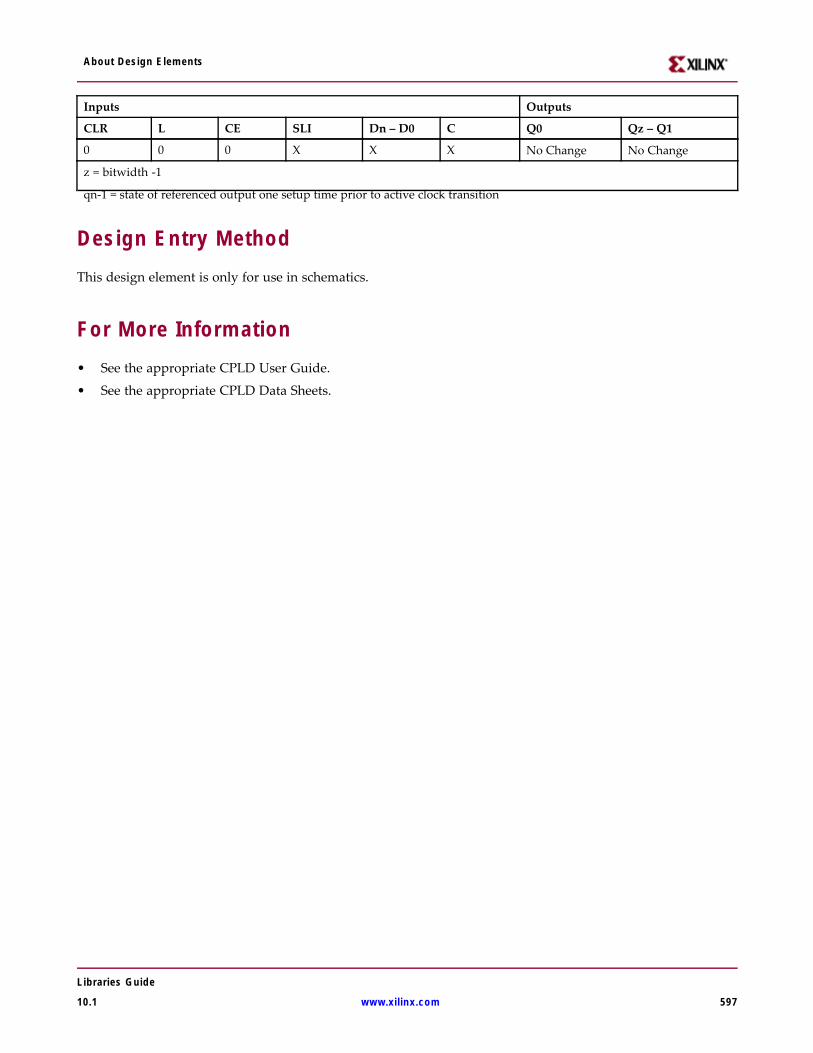
About Design Elements
Inputs Outputs
CLR L CE SLI Dn – D0 C Q0 Qz – Q1
0 0 0 X X X No Change No Change
z = bitwidth -1
qn-1 = state of referenced output one setup time prior to active clock transition
Design Entry MethodThis design element is only for use in schematics.
For More Information• See the appropriate CPLD User Guide.
• See the appropriate CPLD Data Sheets.
Libraries Guide
10.1 www.xilinx.com 597

About Design Elements
SR16CLEDMacro: 16-Bit Shift Register with Clock Enable and Asynchronous Clear
Supported ArchitecturesThis design element is supported in the following architectures only:• XC9500XL• CoolRunner XPLA3• CoolRunner-II
IntroductionThis design element is a shift register with shift-left (SLI) and shift-right (SRI) serial inputs, parallel inputs (D),parallel outputs (Q), and four control inputs: clock enable (CE), load enable (L), shift left/right (LEFT), andasynchronous clear (CLR). The register ignores clock transitions when (CE) and (L) are Low. The asynchronousclear, when High, overrides all other inputs and resets the data outputs (Qn) Low.
When (L) is High and (CLR) is Low, the data on the (D) inputs is loaded into the corresponding (Q) bits of theregister. When (CE) is High and (L) and (CLR) are Low, data is shifted right or left, depending on the state of theLEFT input. If LEFT is High, data on the SLI is loaded into (Q0) during the Low-to-High clock transition andshifted left (for example, to Q1 or Q2) during subsequent clock transitions. If LEFT is Low, data on the SRI isloaded into the last (Q) output during the Low-to-High clock transition and shifted right during subsequentclock transitions. The logic tables indicate the state of the (Q) outputs under all input conditions.
This register is asynchronously cleared, outputs Low, when power is applied.
Logic TableInputs Outputs
CLR L CE LEFT SLI SRID15 –D0 C Q0 Q15
Q14 –Q1
1 X X X X X X X 0 0 0
0 1 X X X X D15 –D0 ↑ D0 D15 Dn
0 0 0 X X X X X NoChange
NoChange
NoChange
Libraries Guide
598 www.xilinx.com 10.1
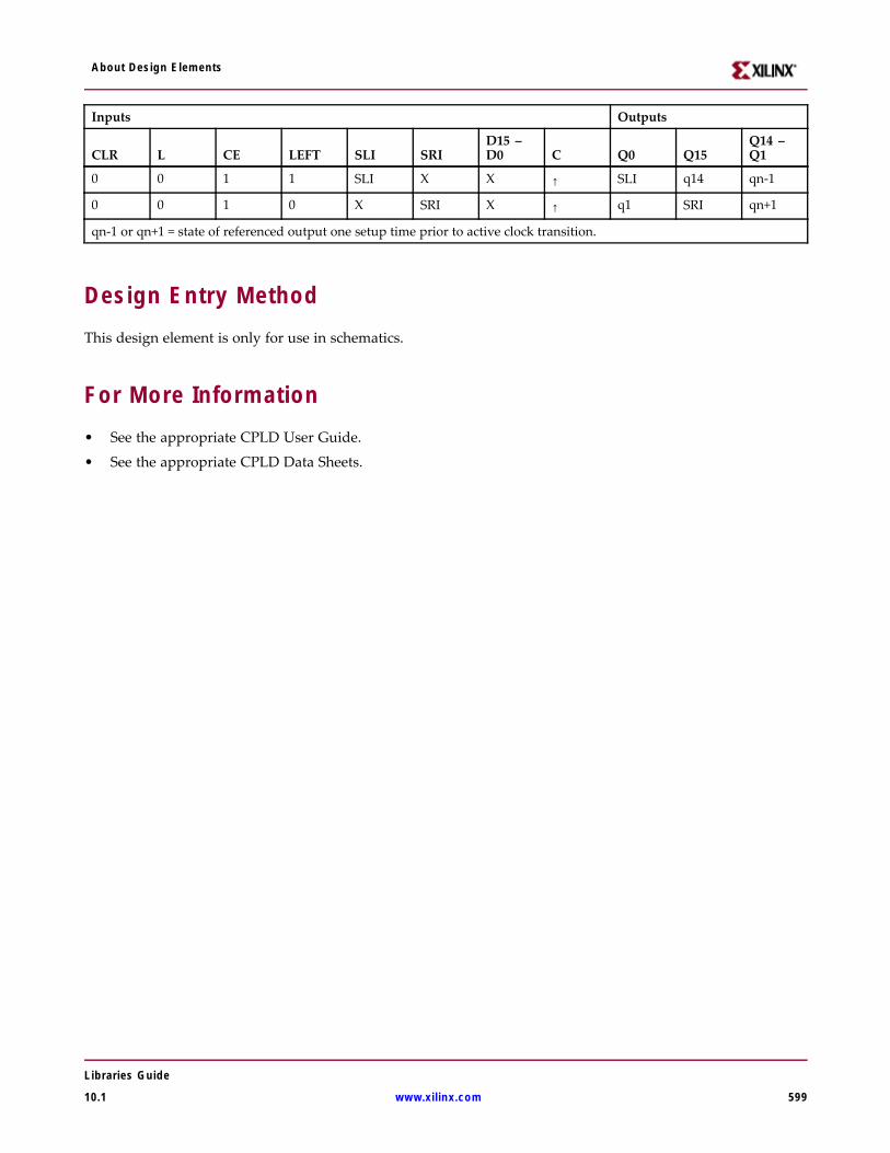
About Design Elements
Inputs Outputs
CLR L CE LEFT SLI SRID15 –D0 C Q0 Q15
Q14 –Q1
0 0 1 1 SLI X X ↑ SLI q14 qn-1
0 0 1 0 X SRI X ↑ q1 SRI qn+1
qn-1 or qn+1 = state of referenced output one setup time prior to active clock transition.
Design Entry MethodThis design element is only for use in schematics.
For More Information• See the appropriate CPLD User Guide.
• See the appropriate CPLD Data Sheets.
Libraries Guide
10.1 www.xilinx.com 599

About Design Elements
SR16REMacro: 16-Bit Serial-In Parallel-Out Shift Register with Clock Enable and Synchronous Reset
Supported ArchitecturesThis design element is supported in the following architectures only:• XC9500XL• CoolRunner XPLA3• CoolRunner-II
IntroductionThis design element is a shift register with shift-left serial input (SLI), parallel outputs (Qn), clock enable (CE),and synchronous reset (R) inputs. The R input, when High, overrides all other inputs during the Low-to-Highclock (C) transition and resets the data outputs (Q) Low.
When (CE) is High and (R) is Low, the data on the (SLI) is loaded into the first bit of the shift register duringthe Low-to-High clock (C) transition and appears on the (Q0) output. During subsequent Low-to-High clocktransitions, when (CE) is High and R is Low, data shifts to the next highest bit position as new data is loaded into(Q0) (for example, SLI→Q0, Q0→Q1, and Q1→Q2). The register ignores clock transitions when (CE) is Low.
Registers can be cascaded by connecting the last (Q) output of one stage to the SLI input of the next stage andconnecting clock, (CE), and (R) in parallel.
This register is asynchronously cleared, outputs Low, when power is applied.
Logic TableInputs Outputs
R CE SLI C Q0 Qz – Q1
1 X X ↑ 0 0
0 0 X X No Change No Change
0 1 SLI ↑ SLI qn-1
z = bitwidth -1
qn-1 = state of referenced output one setup time prior to active clock transition
Design Entry MethodThis design element is only for use in schematics.
Libraries Guide
600 www.xilinx.com 10.1

About Design Elements
For More Information• See the appropriate CPLD User Guide.
• See the appropriate CPLD Data Sheets.
Libraries Guide
10.1 www.xilinx.com 601

About Design Elements
SR16RLEMacro: 16-Bit Loadable Serial/Parallel-In Parallel-Out Shift Register with Clock Enable andSynchronous Reset
Supported ArchitecturesThis design element is supported in the following architectures only:• XC9500XL• CoolRunner XPLA3• CoolRunner-II
IntroductionThis design element is a shift register with shift-left serial input (SLI), parallel inputs (D), parallel outputs (Q),and three control inputs: clock enable (CE), load enable (L), and synchronous reset (R). The register ignores clocktransitions when (L) and (CE) are Low. The synchronous (R), when High, overrides all other inputs during theLow-to-High clock (C) transition and resets the data outputs (Q) Low. When (L) is High and (R) is Low duringthe Low-to-High clock transition, data on the (D) inputs is loaded into the corresponding Q bits of the register.
When (CE) is High and (L) and (R) are Low, data on the (SLI) input is loaded into the first bit of the shiftregister during the Low-to-High clock (C) transition and appears on the Q0 output. During subsequent clocktransitions, when (CE) is High and (L) and (R) are Low, the data shifts to the next highest bit position as newdata is loaded into Q0.
Registers can be cascaded by connecting the last Q output of one stage to the SLI input of the next stage andconnecting clock, (CE), (L), and (R) inputs in parallel.
This register is asynchronously cleared, outputs Low, when power is applied.
Logic TableInputs Outputs
R L CE SLI Dz – D0 C Q0 Qz – Q1
1 X X X X ↑ 0 0
0 1 X X Dz – D0 ↑ D0 Dn
0 0 1 SLI X ↑ SLI qn-1
Libraries Guide
602 www.xilinx.com 10.1

About Design Elements
Inputs Outputs
R L CE SLI Dz – D0 C Q0 Qz – Q1
0 0 0 X X X No Change No Change
z = bitwidth -1
qn-1 = state of referenced output one setup time prior to active clock transition
Design Entry MethodThis design element is only for use in schematics.
For More Information• See the appropriate CPLD User Guide.
• See the appropriate CPLD Data Sheets.
Libraries Guide
10.1 www.xilinx.com 603
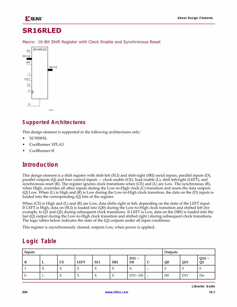
About Design Elements
SR16RLED
Macro: 16-Bit Shift Register with Clock Enable and Synchronous Reset
Supported ArchitecturesThis design element is supported in the following architectures only:• XC9500XL• CoolRunner XPLA3• CoolRunner-II
IntroductionThis design element is a shift register with shift-left (SLI) and shift-right (SRI) serial inputs, parallel inputs (D),parallel outputs (Q) and four control inputs — clock enable (CE), load enable (L), shift left/right (LEFT), andsynchronous reset (R). The register ignores clock transitions when (CE) and (L) are Low. The synchronous (R),when High, overrides all other inputs during the Low-to-High clock (C) transition and resets the data outputs(Q) Low. When (L) is High and (R) is Low during the Low-to-High clock transition, the data on the (D) inputs isloaded into the corresponding (Q) bits of the register.
When (CE) is High and (L) and (R) are Low, data shifts right or left, depending on the state of the LEFT input.If LEFT is High, data on (SLI) is loaded into (Q0) during the Low-to-High clock transition and shifted left (forexample, to Q1 and Q2) during subsequent clock transitions. If LEFT is Low, data on the (SRI) is loaded into thelast (Q) output during the Low-to-High clock transition and shifted right ) during subsequent clock transitions.The logic tables below indicates the state of the (Q) outputs under all input conditions.
This register is asynchronously cleared, outputs Low, when power is applied.
Logic TableInputs Outputs
R L CE LEFT SLI SRID15 –D0 C Q0 Q15
Q14 –Q1
1 X X X X X X ↑ 0 0 0
0 1 X X X X D15 –D0 ↑ D0 D15 Dn
Libraries Guide
604 www.xilinx.com 10.1

About Design Elements
Inputs Outputs
R L CE LEFT SLI SRID15 –D0 C Q0 Q15
Q14 –Q1
0 0 0 X X X X X NoChange
NoChange
NoChange
0 0 1 1 SLI X X ↑ SLI q14 qn-1
0 0 1 0 X SRI X ↑ q1 SRI qn+1
qn-1 or qn+1 = state of referenced output one setup time prior to active clock transition
Design Entry MethodThis design element is only for use in schematics.
For More Information• See the appropriate CPLD User Guide.
• See the appropriate CPLD Data Sheets.
Libraries Guide
10.1 www.xilinx.com 605

About Design Elements
SR4CEMacro: 4-Bit Serial-In Parallel-Out Shift Register with Clock Enable and Asynchronous Clear
Supported ArchitecturesThis design element is supported in the following architectures only:• XC9500XL• CoolRunner XPLA3• CoolRunner-II
IntroductionThis design element is a shift register with a shift-left serial input (SLI), parallel outputs (Q), and clock enable(CE) and asynchronous clear (CLR) inputs. The (CLR) input, when High, overrides all other inputs and resets thedata outputs (Q) Low. When (CE) is High and (CLR) is Low, the data on the SLI input is loaded into the firstbit of the shift register during the Low-to- High clock (C) transition and appears on the (Q0) output. Duringsubsequent Low-to- High clock transitions, when (CE) is High and (CLR) is Low, data shifts to the next highestbit position as new data is loaded into (Q0) (SLI→Q0, Q0→Q1, Q1→Q2, and so forth). The register ignores clocktransitions when (CE) is Low.
Registers can be cascaded by connecting the last (Q) output of one stage to the SLI input of the next stageand connecting clock, (CE), and (CLR) in parallel.
This register is asynchronously cleared, outputs Low, when power is applied.
Logic TableInputs Outputs
CLR CE SLI C Q0 Qz – Q1
1 X X X 0 0
0 0 X X No Change No Change
0 1 SLI ↑ SLI qn-1
z = bit width - 1
qn-1 = state of referenced output one setup time prior to active clock transition
Design Entry MethodThis design element is only for use in schematics.
Libraries Guide
606 www.xilinx.com 10.1

About Design Elements
For More Information• See the appropriate CPLD User Guide.
• See the appropriate CPLD Data Sheets.
Libraries Guide
10.1 www.xilinx.com 607
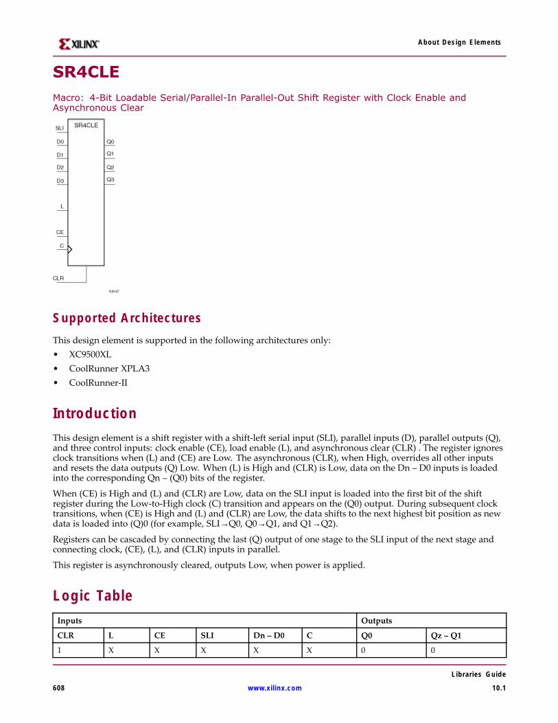
About Design Elements
SR4CLEMacro: 4-Bit Loadable Serial/Parallel-In Parallel-Out Shift Register with Clock Enable andAsynchronous Clear
Supported ArchitecturesThis design element is supported in the following architectures only:• XC9500XL• CoolRunner XPLA3• CoolRunner-II
IntroductionThis design element is a shift register with a shift-left serial input (SLI), parallel inputs (D), parallel outputs (Q),and three control inputs: clock enable (CE), load enable (L), and asynchronous clear (CLR) . The register ignoresclock transitions when (L) and (CE) are Low. The asynchronous (CLR), when High, overrides all other inputsand resets the data outputs (Q) Low. When (L) is High and (CLR) is Low, data on the Dn – D0 inputs is loadedinto the corresponding Qn – (Q0) bits of the register.
When (CE) is High and (L) and (CLR) are Low, data on the SLI input is loaded into the first bit of the shiftregister during the Low-to-High clock (C) transition and appears on the (Q0) output. During subsequent clocktransitions, when (CE) is High and (L) and (CLR) are Low, the data shifts to the next highest bit position as newdata is loaded into (Q)0 (for example, SLI→Q0, Q0→Q1, and Q1→Q2).
Registers can be cascaded by connecting the last (Q) output of one stage to the SLI input of the next stage andconnecting clock, (CE), (L), and (CLR) inputs in parallel.
This register is asynchronously cleared, outputs Low, when power is applied.
Logic TableInputs Outputs
CLR L CE SLI Dn – D0 C Q0 Qz – Q1
1 X X X X X 0 0
Libraries Guide
608 www.xilinx.com 10.1

About Design Elements
Inputs Outputs
CLR L CE SLI Dn – D0 C Q0 Qz – Q1
0 1 X X Dn – D0 ↑ D0 Dn
0 0 1 SLI X ↑ SLI qn-1
0 0 0 X X X No Change No Change
z = bitwidth -1
qn-1 = state of referenced output one setup time prior to active clock transition
Design Entry MethodThis design element is only for use in schematics.
For More Information• See the appropriate CPLD User Guide.
• See the appropriate CPLD Data Sheets.
Libraries Guide
10.1 www.xilinx.com 609

About Design Elements
SR4CLED
Macro: 4-Bit Shift Register with Clock Enable and Asynchronous Clear
Supported ArchitecturesThis design element is supported in the following architectures only:• XC9500XL• CoolRunner XPLA3• CoolRunner-II
IntroductionThis design element is a shift register with shift-left (SLI) and shift-right (SRI) serial inputs, parallel inputs (D),parallel outputs (Q), and four control inputs: clock enable (CE), load enable (L), shift left/right (LEFT), andasynchronous clear (CLR). The register ignores clock transitions when (CE) and (L) are Low. The asynchronousclear, when High, overrides all other inputs and resets the data outputs (Qn) Low.
When (L) is High and (CLR) is Low, the data on the (D) inputs is loaded into the corresponding (Q) bits of theregister. When (CE) is High and (L) and (CLR) are Low, data is shifted right or left, depending on the state of theLEFT input. If LEFT is High, data on the SLI is loaded into (Q0) during the Low-to-High clock transition andshifted left (for example, to Q1 or Q2) during subsequent clock transitions. If LEFT is Low, data on the SRI isloaded into the last (Q) output during the Low-to-High clock transition and shifted right during subsequentclock transitions. The logic tables indicate the state of the (Q) outputs under all input conditions.
This register is asynchronously cleared, outputs Low, when power is applied.
Logic TableInputs Outputs
CLR L CE LEFT SLI SRI D3 – D0 C Q0 Q3 Q2 – Q1
1 X X X X X X X 0 0 0
0 1 X X X X D3– D0 ↑ D0 D3 Dn
Libraries Guide
610 www.xilinx.com 10.1

About Design Elements
Inputs Outputs
CLR L CE LEFT SLI SRI D3 – D0 C Q0 Q3 Q2 – Q1
0 0 0 X X X X X NoChange
NoChange
NoChange
0 0 1 1 SLI X X ↑ SLI q2 qn-1
0 0 1 0 X SRI X ↑ q1 SRI qn+1
qn-1 and qn+1 = state of referenced output one setup time prior to active clock transition.
Design Entry MethodThis design element is only for use in schematics.
For More Information• See the appropriate CPLD User Guide.
• See the appropriate CPLD Data Sheets.
Libraries Guide
10.1 www.xilinx.com 611

About Design Elements
SR4REMacro: 4-Bit Serial-In Parallel-Out Shift Register with Clock Enable and Synchronous Reset
Supported ArchitecturesThis design element is supported in the following architectures only:• XC9500XL• CoolRunner XPLA3• CoolRunner-II
IntroductionThis design element is a shift register with shift-left serial input (SLI), parallel outputs (Qn), clock enable (CE),and synchronous reset (R) inputs. The R input, when High, overrides all other inputs during the Low-to-Highclock (C) transition and resets the data outputs (Q) Low.
When (CE) is High and (R) is Low, the data on the (SLI) is loaded into the first bit of the shift register duringthe Low-to-High clock (C) transition and appears on the (Q0) output. During subsequent Low-to-High clocktransitions, when (CE) is High and R is Low, data shifts to the next highest bit position as new data is loaded into(Q0) (for example, SLI→Q0, Q0→Q1, and Q1→Q2). The register ignores clock transitions when (CE) is Low.
Registers can be cascaded by connecting the last (Q) output of one stage to the SLI input of the next stage andconnecting clock, (CE), and (R) in parallel.
This register is asynchronously cleared, outputs Low, when power is applied.
Logic TableInputs Outputs
R CE SLI C Q0 Qz – Q1
1 X X ↑ 0 0
0 0 X X No Change No Change
0 1 SLI ↑ SLI qn-1
z = bitwidth -1
qn-1 = state of referenced output one setup time prior to active clock transition
Design Entry MethodThis design element is only for use in schematics.
Libraries Guide
612 www.xilinx.com 10.1

About Design Elements
For More Information• See the appropriate CPLD User Guide.
• See the appropriate CPLD Data Sheets.
Libraries Guide
10.1 www.xilinx.com 613
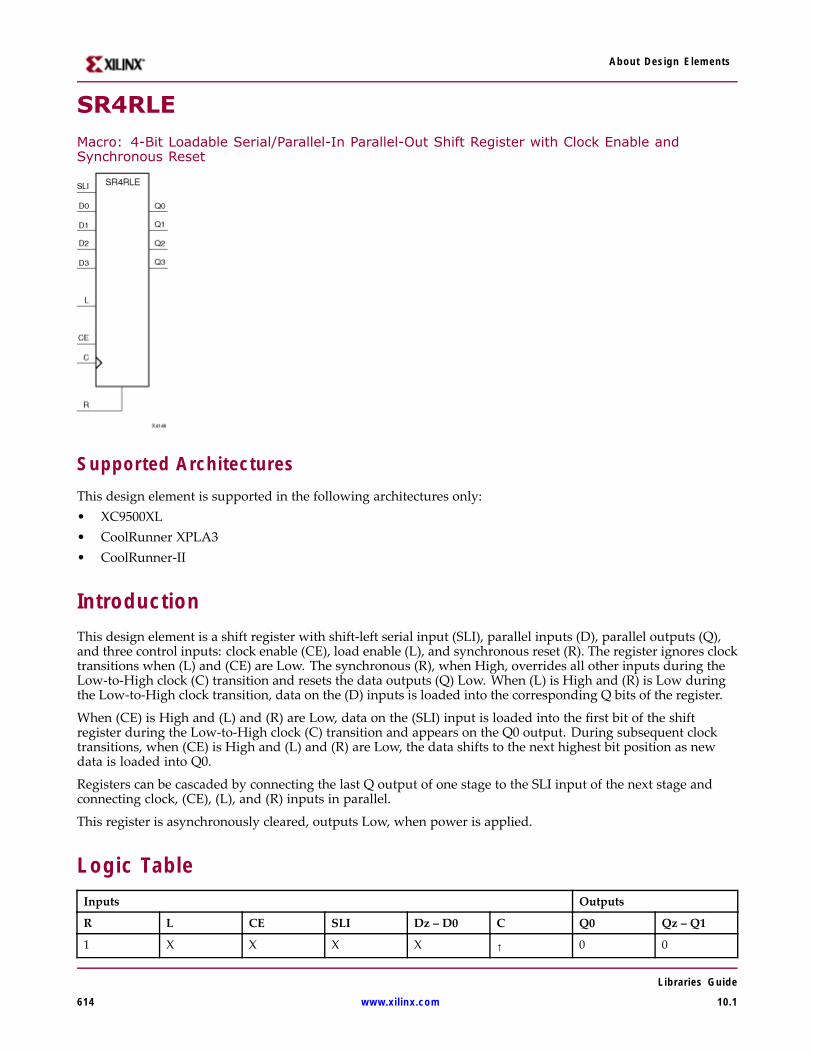
About Design Elements
SR4RLEMacro: 4-Bit Loadable Serial/Parallel-In Parallel-Out Shift Register with Clock Enable andSynchronous Reset
Supported ArchitecturesThis design element is supported in the following architectures only:• XC9500XL• CoolRunner XPLA3• CoolRunner-II
IntroductionThis design element is a shift register with shift-left serial input (SLI), parallel inputs (D), parallel outputs (Q),and three control inputs: clock enable (CE), load enable (L), and synchronous reset (R). The register ignores clocktransitions when (L) and (CE) are Low. The synchronous (R), when High, overrides all other inputs during theLow-to-High clock (C) transition and resets the data outputs (Q) Low. When (L) is High and (R) is Low duringthe Low-to-High clock transition, data on the (D) inputs is loaded into the corresponding Q bits of the register.
When (CE) is High and (L) and (R) are Low, data on the (SLI) input is loaded into the first bit of the shiftregister during the Low-to-High clock (C) transition and appears on the Q0 output. During subsequent clocktransitions, when (CE) is High and (L) and (R) are Low, the data shifts to the next highest bit position as newdata is loaded into Q0.
Registers can be cascaded by connecting the last Q output of one stage to the SLI input of the next stage andconnecting clock, (CE), (L), and (R) inputs in parallel.
This register is asynchronously cleared, outputs Low, when power is applied.
Logic TableInputs Outputs
R L CE SLI Dz – D0 C Q0 Qz – Q1
1 X X X X ↑ 0 0
Libraries Guide
614 www.xilinx.com 10.1

About Design Elements
Inputs Outputs
R L CE SLI Dz – D0 C Q0 Qz – Q1
0 1 X X Dz – D0 ↑ D0 Dn
0 0 1 SLI X ↑ SLI qn-1
0 0 0 X X X No Change No Change
z = bitwidth -1
qn-1 = state of referenced output one setup time prior to active clock transition
Design Entry MethodThis design element is only for use in schematics.
For More Information• See the appropriate CPLD User Guide.
• See the appropriate CPLD Data Sheets.
Libraries Guide
10.1 www.xilinx.com 615
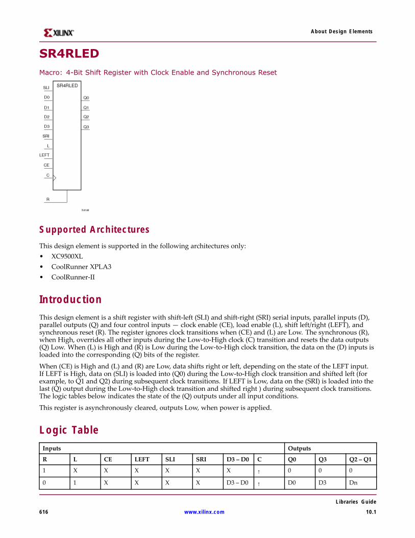
About Design Elements
SR4RLEDMacro: 4-Bit Shift Register with Clock Enable and Synchronous Reset
Supported ArchitecturesThis design element is supported in the following architectures only:• XC9500XL• CoolRunner XPLA3• CoolRunner-II
IntroductionThis design element is a shift register with shift-left (SLI) and shift-right (SRI) serial inputs, parallel inputs (D),parallel outputs (Q) and four control inputs — clock enable (CE), load enable (L), shift left/right (LEFT), andsynchronous reset (R). The register ignores clock transitions when (CE) and (L) are Low. The synchronous (R),when High, overrides all other inputs during the Low-to-High clock (C) transition and resets the data outputs(Q) Low. When (L) is High and (R) is Low during the Low-to-High clock transition, the data on the (D) inputs isloaded into the corresponding (Q) bits of the register.
When (CE) is High and (L) and (R) are Low, data shifts right or left, depending on the state of the LEFT input.If LEFT is High, data on (SLI) is loaded into (Q0) during the Low-to-High clock transition and shifted left (forexample, to Q1 and Q2) during subsequent clock transitions. If LEFT is Low, data on the (SRI) is loaded into thelast (Q) output during the Low-to-High clock transition and shifted right ) during subsequent clock transitions.The logic tables below indicates the state of the (Q) outputs under all input conditions.
This register is asynchronously cleared, outputs Low, when power is applied.
Logic TableInputs Outputs
R L CE LEFT SLI SRI D3 – D0 C Q0 Q3 Q2 – Q1
1 X X X X X X ↑ 0 0 0
0 1 X X X X D3 – D0 ↑ D0 D3 Dn
Libraries Guide
616 www.xilinx.com 10.1
About Design Elements
Inputs Outputs
R L CE LEFT SLI SRI D3 – D0 C Q0 Q3 Q2 – Q1
0 0 0 X X X X X NoChange
NoChange
NoChange
0 0 1 1 SLI X X ↑ SLI q2 qn-1
0 0 1 0 X SRI X ↑ q1 SRI qn+1
qn-1 or qn+1 = state of referenced output one setup time prior to active clock transition
Design Entry MethodThis design element is only for use in schematics.
For More Information• See the appropriate CPLD User Guide.
• See the appropriate CPLD Data Sheets.
Libraries Guide
10.1 www.xilinx.com 617
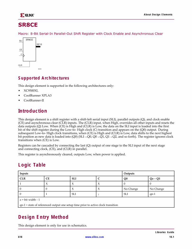
About Design Elements
SR8CEMacro: 8-Bit Serial-In Parallel-Out Shift Register with Clock Enable and Asynchronous Clear
Supported ArchitecturesThis design element is supported in the following architectures only:• XC9500XL• CoolRunner XPLA3• CoolRunner-II
IntroductionThis design element is a shift register with a shift-left serial input (SLI), parallel outputs (Q), and clock enable(CE) and asynchronous clear (CLR) inputs. The (CLR) input, when High, overrides all other inputs and resets thedata outputs (Q) Low. When (CE) is High and (CLR) is Low, the data on the SLI input is loaded into the firstbit of the shift register during the Low-to- High clock (C) transition and appears on the (Q0) output. Duringsubsequent Low-to- High clock transitions, when (CE) is High and (CLR) is Low, data shifts to the next highestbit position as new data is loaded into (Q0) (SLI→Q0, Q0→Q1, Q1→Q2, and so forth). The register ignores clocktransitions when (CE) is Low.
Registers can be cascaded by connecting the last (Q) output of one stage to the SLI input of the next stageand connecting clock, (CE), and (CLR) in parallel.
This register is asynchronously cleared, outputs Low, when power is applied.
Logic TableInputs Outputs
CLR CE SLI C Q0 Qz – Q1
1 X X X 0 0
0 0 X X No Change No Change
0 1 SLI ↑ SLI qn-1
z = bit width - 1
qn-1 = state of referenced output one setup time prior to active clock transition
Design Entry MethodThis design element is only for use in schematics.
Libraries Guide
618 www.xilinx.com 10.1

About Design Elements
For More Information• See the appropriate CPLD User Guide.
• See the appropriate CPLD Data Sheets.
Libraries Guide
10.1 www.xilinx.com 619

About Design Elements
SR8CLEMacro: 8-Bit Loadable Serial/Parallel-In Parallel-Out Shift Register with Clock Enable andAsynchronous Clear
Supported ArchitecturesThis design element is supported in the following architectures only:• XC9500XL• CoolRunner XPLA3• CoolRunner-II
IntroductionThis design element is a shift register with a shift-left serial input (SLI), parallel inputs (D), parallel outputs (Q),and three control inputs: clock enable (CE), load enable (L), and asynchronous clear (CLR) . The register ignoresclock transitions when (L) and (CE) are Low. The asynchronous (CLR), when High, overrides all other inputsand resets the data outputs (Q) Low. When (L) is High and (CLR) is Low, data on the Dn – D0 inputs is loadedinto the corresponding Qn – (Q0) bits of the register.
When (CE) is High and (L) and (CLR) are Low, data on the SLI input is loaded into the first bit of the shiftregister during the Low-to-High clock (C) transition and appears on the (Q0) output. During subsequent clocktransitions, when (CE) is High and (L) and (CLR) are Low, the data shifts to the next highest bit position as newdata is loaded into (Q)0 (for example, SLI→Q0, Q0→Q1, and Q1→Q2).
Registers can be cascaded by connecting the last (Q) output of one stage to the SLI input of the next stage andconnecting clock, (CE), (L), and (CLR) inputs in parallel.
This register is asynchronously cleared, outputs Low, when power is applied.
Logic TableInputs Outputs
CLR L CE SLI Dn – D0 C Q0 Qz – Q1
1 X X X X X 0 0
0 1 X X Dn – D0 ↑ D0 Dn
0 0 1 SLI X ↑ SLI qn-1
Libraries Guide
620 www.xilinx.com 10.1

About Design Elements
Inputs Outputs
CLR L CE SLI Dn – D0 C Q0 Qz – Q1
0 0 0 X X X No Change No Change
z = bitwidth -1
qn-1 = state of referenced output one setup time prior to active clock transition
Design Entry MethodThis design element is only for use in schematics.
For More Information• See the appropriate CPLD User Guide.
• See the appropriate CPLD Data Sheets.
Libraries Guide
10.1 www.xilinx.com 621

About Design Elements
SR8CLEDMacro: 8-Bit Shift Register with Clock Enable and Asynchronous Clear
Supported ArchitecturesThis design element is supported in the following architectures only:• XC9500XL• CoolRunner XPLA3• CoolRunner-II
IntroductionThis design element is a shift register with shift-left (SLI) and shift-right (SRI) serial inputs, parallel inputs (D),parallel outputs (Q), and four control inputs: clock enable (CE), load enable (L), shift left/right (LEFT), andasynchronous clear (CLR). The register ignores clock transitions when (CE) and (L) are Low. The asynchronousclear, when High, overrides all other inputs and resets the data outputs (Qn) Low.
When (L) is High and (CLR) is Low, the data on the (D) inputs is loaded into the corresponding (Q) bits of theregister. When (CE) is High and (L) and (CLR) are Low, data is shifted right or left, depending on the state of theLEFT input. If LEFT is High, data on the SLI is loaded into (Q0) during the Low-to-High clock transition andshifted left (for example, to Q1 or Q2) during subsequent clock transitions. If LEFT is Low, data on the SRI isloaded into the last (Q) output during the Low-to-High clock transition and shifted right during subsequentclock transitions. The logic tables indicate the state of the (Q) outputs under all input conditions.
This register is asynchronously cleared, outputs Low, when power is applied.
Logic TableInputs Outputs
CLR L CE LEFT SLI SRI D7 – D0 C Q0 Q7 Q6 – Q1
1 X X X X X X X 0 0 0
0 1 X X X X D7 – D0 ↑ D0 D7 Dn
0 0 0 X X X X X NoChange
NoChange
NoChange
0 0 1 1 SLI X X ↑ SLI q6 qn-1
Libraries Guide
622 www.xilinx.com 10.1

About Design Elements
Inputs Outputs
CLR L CE LEFT SLI SRI D7 – D0 C Q0 Q7 Q6 – Q1
0 0 1 0 X SRI X ↑ q1 SRI qn+1
qn-1 or qn+1 = state of referenced output one setup time prior to active clock transition.
Design Entry MethodThis design element is only for use in schematics.
For More Information• See the appropriate CPLD User Guide.
• See the appropriate CPLD Data Sheets.
Libraries Guide
10.1 www.xilinx.com 623

About Design Elements
SR8REMacro: 8-Bit Serial-In Parallel-Out Shift Register with Clock Enable and Synchronous Reset
Supported ArchitecturesThis design element is supported in the following architectures only:• XC9500XL• CoolRunner XPLA3• CoolRunner-II
IntroductionThis design element is a shift register with shift-left serial input (SLI), parallel outputs (Qn), clock enable (CE),and synchronous reset (R) inputs. The R input, when High, overrides all other inputs during the Low-to-Highclock (C) transition and resets the data outputs (Q) Low.
When (CE) is High and (R) is Low, the data on the (SLI) is loaded into the first bit of the shift register duringthe Low-to-High clock (C) transition and appears on the (Q0) output. During subsequent Low-to-High clocktransitions, when (CE) is High and R is Low, data shifts to the next highest bit position as new data is loaded into(Q0) (for example, SLI→Q0, Q0→Q1, and Q1→Q2). The register ignores clock transitions when (CE) is Low.
Registers can be cascaded by connecting the last (Q) output of one stage to the SLI input of the next stage andconnecting clock, (CE), and (R) in parallel.
This register is asynchronously cleared, outputs Low, when power is applied.
Logic TableInputs Outputs
R CE SLI C Q0 Qz – Q1
1 X X ↑ 0 0
0 0 X X No Change No Change
0 1 SLI ↑ SLI qn-1
z = bitwidth -1
qn-1 = state of referenced output one setup time prior to active clock transition
Design Entry MethodThis design element is only for use in schematics.
Libraries Guide
624 www.xilinx.com 10.1

About Design Elements
For More Information• See the appropriate CPLD User Guide.
• See the appropriate CPLD Data Sheets.
Libraries Guide
10.1 www.xilinx.com 625

About Design Elements
SR8RLEMacro: 8-Bit Loadable Serial/Parallel-In Parallel-Out Shift Register with Clock Enable andSynchronous Reset
Supported ArchitecturesThis design element is supported in the following architectures only:• XC9500XL• CoolRunner XPLA3• CoolRunner-II
IntroductionThis design element is a shift register with shift-left serial input (SLI), parallel inputs (D), parallel outputs (Q),and three control inputs: clock enable (CE), load enable (L), and synchronous reset (R). The register ignores clocktransitions when (L) and (CE) are Low. The synchronous (R), when High, overrides all other inputs during theLow-to-High clock (C) transition and resets the data outputs (Q) Low. When (L) is High and (R) is Low duringthe Low-to-High clock transition, data on the (D) inputs is loaded into the corresponding Q bits of the register.
When (CE) is High and (L) and (R) are Low, data on the (SLI) input is loaded into the first bit of the shiftregister during the Low-to-High clock (C) transition and appears on the Q0 output. During subsequent clocktransitions, when (CE) is High and (L) and (R) are Low, the data shifts to the next highest bit position as newdata is loaded into Q0.
Registers can be cascaded by connecting the last Q output of one stage to the SLI input of the next stage andconnecting clock, (CE), (L), and (R) inputs in parallel.
This register is asynchronously cleared, outputs Low, when power is applied.
Logic TableInputs Outputs
R L CE SLI Dz – D0 C Q0 Qz – Q1
1 X X X X ↑ 0 0
0 1 X X Dz – D0 ↑ D0 Dn
0 0 1 SLI X ↑ SLI qn-1
Libraries Guide
626 www.xilinx.com 10.1
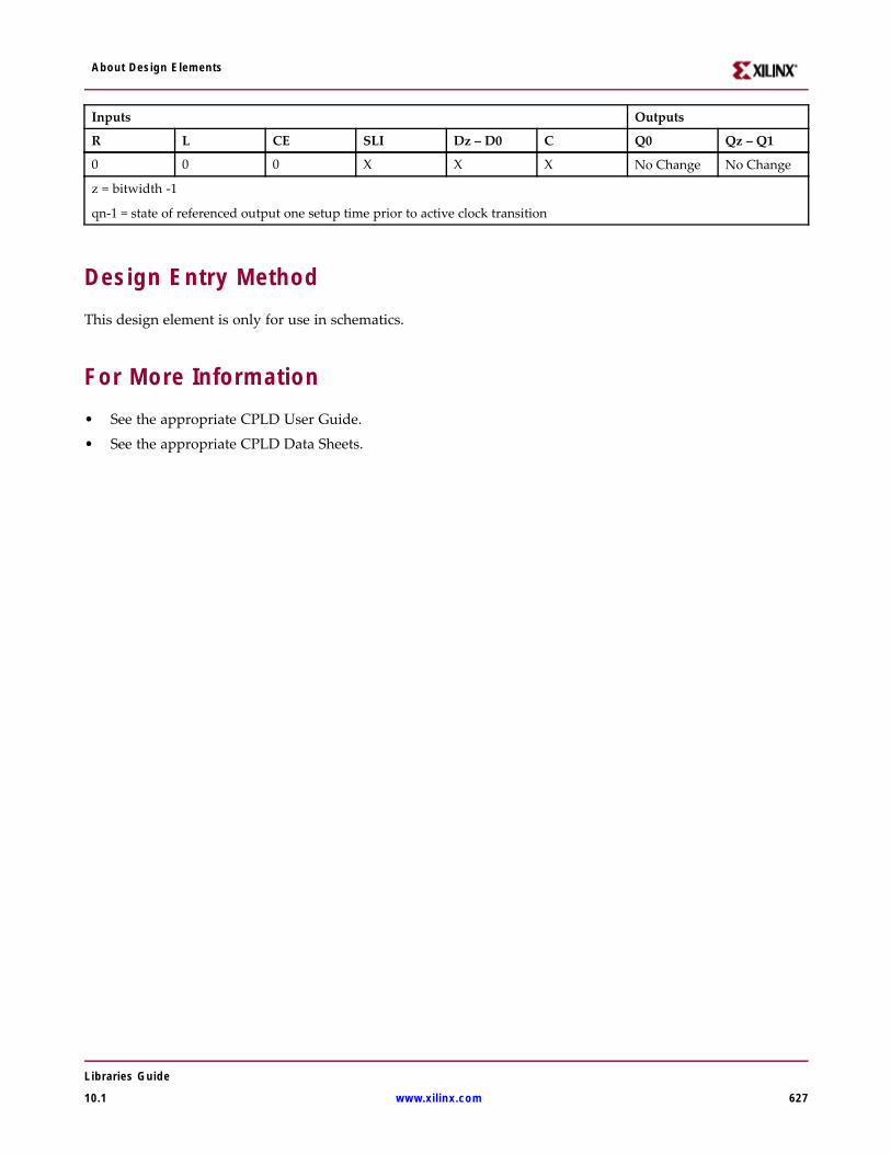
About Design Elements
Inputs Outputs
R L CE SLI Dz – D0 C Q0 Qz – Q1
0 0 0 X X X No Change No Change
z = bitwidth -1
qn-1 = state of referenced output one setup time prior to active clock transition
Design Entry MethodThis design element is only for use in schematics.
For More Information• See the appropriate CPLD User Guide.
• See the appropriate CPLD Data Sheets.
Libraries Guide
10.1 www.xilinx.com 627

About Design Elements
SR8RLEDMacro: 8-Bit Shift Register with Clock Enable and Synchronous Reset
Supported ArchitecturesThis design element is supported in the following architectures only:• XC9500XL• CoolRunner XPLA3• CoolRunner-II
IntroductionThis design element is a shift register with shift-left (SLI) and shift-right (SRI) serial inputs, parallel inputs (D),parallel outputs (Q) and four control inputs — clock enable (CE), load enable (L), shift left/right (LEFT), andsynchronous reset (R). The register ignores clock transitions when (CE) and (L) are Low. The synchronous (R),when High, overrides all other inputs during the Low-to-High clock (C) transition and resets the data outputs(Q) Low. When (L) is High and (R) is Low during the Low-to-High clock transition, the data on the (D) inputs isloaded into the corresponding (Q) bits of the register.
When (CE) is High and (L) and (R) are Low, data shifts right or left, depending on the state of the LEFT input.If LEFT is High, data on (SLI) is loaded into (Q0) during the Low-to-High clock transition and shifted left (forexample, to Q1 and Q2) during subsequent clock transitions. If LEFT is Low, data on the (SRI) is loaded into thelast (Q) output during the Low-to-High clock transition and shifted right ) during subsequent clock transitions.The logic tables below indicates the state of the (Q) outputs under all input conditions.
This register is asynchronously cleared, outputs Low, when power is applied.
Logic TableInputs Outputs
R L CE LEFT SLI SRI D7– D0 C Q0 Q7 Q6 – Q1
1 X X X X X X ↑ 0 0 0
0 1 X X X X D7 – D0 ↑ D0 D7 Dn
0 0 0 X X X X X NoChange
NoChange
NoChange
Libraries Guide
628 www.xilinx.com 10.1

About Design Elements
Inputs Outputs
R L CE LEFT SLI SRI D7– D0 C Q0 Q7 Q6 – Q1
0 0 1 1 SLI X X ↑ SLI q6 qn-1
0 0 1 0 X SRI X ↑ q1 SRI qn+1
qn-1 or qn+1 = state of referenced output one setup time prior to active clock transition
Design Entry MethodThis design element is only for use in schematics.
For More Information• See the appropriate CPLD User Guide.
• See the appropriate CPLD Data Sheets.
Libraries Guide
10.1 www.xilinx.com 629

About Design Elements
SRD16CE
Macro: 16-Bit Serial-In Parallel-Out Dual Edge Triggered Shift Register with Clock Enable andAsynchronous Clear
Supported Architectures
This design element is supported in the following architectures only:CoolRunner-II
IntroductionThis design element is a dual edge triggered shift register with a shift-left serial input (SLI), parallel outputs (Q),clock enable (CE) and asynchronous clear (CLR) inputs. The CLR input, when High, overrides all other inputsand resets the data outputs (Q) Low. When CE is High and CLR is Low, the data on the SLI input is loaded intothe first bit of the shift register during the Low-to-High (or High-to-Low) clock (C) transition and appears on theQ0 output. During subsequent clock transitions, when CE is High and CLR is Low, data shifts to the next highestbit position as new data is loaded into Q0. The register ignores clock transitions when CE is Low.
Registers can be cascaded by connecting the last Q output of one stage to the SLI input of the next stage andconnecting clock, CE, and CLR in parallel.
This register is asynchronously cleared, outputs Low, when power is applied. .
The power-on condition can be simulated by applying a High-level pulse on the PRLD global net.
Logic TableInputs Outputs
CLR CE SLI C Q0 Qz – Q1
1 X X X 0 0
0 0 X X No Change No Change
0 1 1 ↑ 1 qn-1
0 1 1 ↓ 1 qn-1
0 1 0 ↑ 0 qn-1
0 1 0 ↓ 0 qn-1
z = bitwidth -1
qn-1 = state of referenced output one setup time prior to active clock transition
Libraries Guide
630 www.xilinx.com 10.1

About Design Elements
Design Entry MethodThis design element is only for use in schematics.
For More Information• See the appropriate CPLD User Guide.
• See the appropriate CPLD Data Sheets.
Libraries Guide
10.1 www.xilinx.com 631
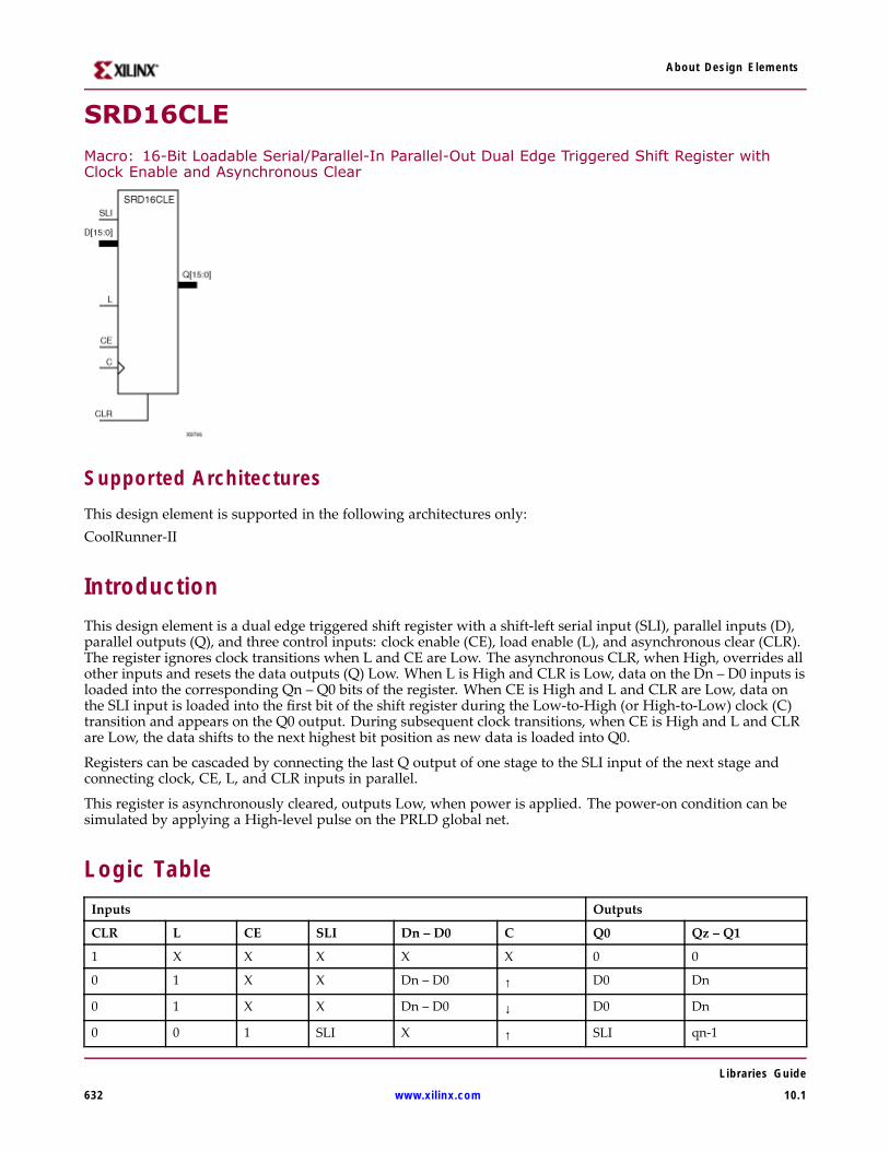
About Design Elements
SRD16CLEMacro: 16-Bit Loadable Serial/Parallel-In Parallel-Out Dual Edge Triggered Shift Register withClock Enable and Asynchronous Clear
Supported ArchitecturesThis design element is supported in the following architectures only:CoolRunner-II
IntroductionThis design element is a dual edge triggered shift register with a shift-left serial input (SLI), parallel inputs (D),parallel outputs (Q), and three control inputs: clock enable (CE), load enable (L), and asynchronous clear (CLR).The register ignores clock transitions when L and CE are Low. The asynchronous CLR, when High, overrides allother inputs and resets the data outputs (Q) Low. When L is High and CLR is Low, data on the Dn – D0 inputs isloaded into the corresponding Qn – Q0 bits of the register. When CE is High and L and CLR are Low, data onthe SLI input is loaded into the first bit of the shift register during the Low-to-High (or High-to-Low) clock (C)transition and appears on the Q0 output. During subsequent clock transitions, when CE is High and L and CLRare Low, the data shifts to the next highest bit position as new data is loaded into Q0.
Registers can be cascaded by connecting the last Q output of one stage to the SLI input of the next stage andconnecting clock, CE, L, and CLR inputs in parallel.
This register is asynchronously cleared, outputs Low, when power is applied. The power-on condition can besimulated by applying a High-level pulse on the PRLD global net.
Logic TableInputs Outputs
CLR L CE SLI Dn – D0 C Q0 Qz – Q1
1 X X X X X 0 0
0 1 X X Dn – D0 ↑ D0 Dn
0 1 X X Dn – D0 ↓ D0 Dn
0 0 1 SLI X ↑ SLI qn-1
Libraries Guide
632 www.xilinx.com 10.1

About Design Elements
Inputs Outputs
CLR L CE SLI Dn – D0 C Q0 Qz – Q1
0 0 1 SLI X ↓ SLI qn-1
0 0 0 X X X No Change No Change
z = bitwidth -1
qn-1 = state of referenced output one setup time prior to active clock transition
Design Entry MethodThis design element is only for use in schematics.
For More Information• See the appropriate CPLD User Guide.
• See the appropriate CPLD Data Sheets.
Libraries Guide
10.1 www.xilinx.com 633

About Design Elements
SRD16CLEDMacro: 16-Bit Dual Edge Triggered Shift Register with Clock Enable and Asynchronous Clear
Supported ArchitecturesThis design element is supported in the following architectures only:CoolRunner-II
IntroductionThis design element is a dual edge triggered shift register with shift-left (SLI) and shift-right (SRI) serial inputs,parallel inputs (D), parallel outputs (Q), and four control inputs: clock enable (CE), load enable (L), shift left/right(LEFT), and asynchronous clear (CLR). The register ignores clock transitions when CE and L are Low. Theasynchronous clear, when High, overrides all other inputs and resets the data outputs (Qn) Low. When L is Highand CLR is Low, the data on the D inputs is loaded into the corresponding Q bits of the register. When CE isHigh and L and CLR are Low, data is shifted right or left, depending on the state of the LEFT input. If LEFT isHigh, data on the SLI is loaded into Q0 during the Low-to-High or High-to-Low clock transition and shifted leftduring subsequent clock transitions. If LEFT is Low, data on the SRI is loaded into the last Q output duringthe Low-to-High or High-to-Low clock transition and shifted right during subsequent clock transitions. Thelogic table indicates the state of the Q outputs under all input conditions.
This register is asynchronously cleared, outputs Low, when power is applied. The power-on condition can besimulated by applying a High-level pulse on the PRLD global net.
Logic TableInputs Outputs
CLR L CE LEFT SLI SRID15 –D0 C Q0 Q15
Q14 –Q1
1 X X X X X X X 0 0 0
0 1 X X X X D15 –D0 ↑ D0 D15 Dn
0 1 X X X X D15 –D0 ↓ D0 D15 Dn
0 0 0 X X X X X NoChange
NoChange
NoChange
0 0 1 1 SLI X X ↑ SLI q14 qn-1
Libraries Guide
634 www.xilinx.com 10.1

About Design Elements
Inputs Outputs
CLR L CE LEFT SLI SRID15 –D0 C Q0 Q15
Q14 –Q1
0 0 1 1 SLI X X ↓ SLI q14 qn-1
0 0 1 0 X SRI X ↑ q1 SRI qn+1
0 0 1 0 X SRI X ↓ q1 SRI qn+1
qn-1 or qn+1 = state of referenced output one setup time prior to active clock transition.
Design Entry MethodThis design element is only for use in schematics.
For More Information• See the appropriate CPLD User Guide.
• See the appropriate CPLD Data Sheets.
Libraries Guide
10.1 www.xilinx.com 635

About Design Elements
SRD16REMacro: 16-Bit Serial-In Parallel-Out Dual Edge Triggered Shift Register with Clock Enable andSynchronous Reset
Supported ArchitecturesThis design element is supported in the following architectures only:CoolRunner-II
IntroductionThis design element is a dual edge triggered shift register with shift-left serial input (SLI), parallel outputs (Qn),clock enable (CE), and synchronous reset (R) inputs. The R input, when High, overrides all other inputs duringthe Low-to-High or High-to-Low clock (C) transition and resets the data outputs (Q) Low. When CE is Highand R is Low, the data on the SLI is loaded into the first bit of the shift register during the Low-to-High clock orHigh-to-Low (C) transition and appears on the Q0 output. During subsequent clock transitions, when CE isHigh and R is Low, data shifts to the next highest bit position as new data is loaded into Q0. The registerignores clock transitions when CE is Low.
Registers can be cascaded by connecting the last Q output of one stage to the SLI input of the next stage andconnecting clock, CE, and R in parallel.
This register is asynchronously cleared, outputs Low, when power is applied. The power-on condition can besimulated by applying a High-level pulse on the PRLD global net.
Logic TableInputs Outputs
R CE SLI C Q0 Qz – Q1
1 X X ↑ 0 0
1 X X ↓ 0 0
0 0 X X No Change No Change
0 1 1 ↑ 1 qn-1
0 1 1 ↓ 1 qn-1
0 1 0 ↑ 0 qn-1
0 1 0 ↓ 0 qn-1
z = bitwidth -1
qn-1 = state of referenced output one setup time prior to active clock transition
Libraries Guide
636 www.xilinx.com 10.1

About Design Elements
Design Entry MethodThis design element is only for use in schematics.
For More Information• See the appropriate CPLD User Guide.
• See the appropriate CPLD Data Sheets.
Libraries Guide
10.1 www.xilinx.com 637

About Design Elements
SRD16RLEMacro: 16-Bit Loadable Serial/Parallel-In Parallel-Out Dual Edge Triggered Shift Register withClock Enable and Synchronous Reset
Supported ArchitecturesThis design element is supported in the following architectures only:CoolRunner-II
IntroductionThis design element is a dual edge triggered shift register with shift-left serial input (SLI), parallel inputs (D),parallel outputs (Q), and three control inputs: clock enable (CE), load enable (L), and synchronous reset (R). Theregister ignores clock transitions when L and CE are Low. The synchronous R, when High, overrides all otherinputs during the Low-to-High or High-to-Low clock (C) transition and resets the data outputs (Q) Low. When Lis High and R is Low, data on the D inputs is loaded into the corresponding Q bits of the register. When CE is Highand L and R are Low, data on the SLI input is loaded into the first bit of the shift register during the Low-to-Highor High-to-Low clock (C) transition and appears on the Q0 output. During subsequent clock transitions, whenCE is High and L and R are Low, the data shifts to the next highest bit position as new data is loaded into Q0.
Registers can be cascaded by connecting the last Q output of one stage to the SLI input of the next stage andconnecting clock, CE, L, and R inputs in parallel.
This register is asynchronously cleared, outputs Low, when power is applied. The power-on condition can besimulated by applying a High-level pulse on the PRLD global net.
Logic TableInputs Outputs
R L CE SLI Dz – D0 C Q0 Qz – Q1
1 X X X X ↑ 0 0
1 X X X X ↓ 0 0
0 1 X X Dz – D0 ↑ D0 Dn
0 1 X X Dz – D0 ↓ D0 Dn
0 0 1 SLI X ↑ SLI qn-1
Libraries Guide
638 www.xilinx.com 10.1

About Design Elements
Inputs Outputs
R L CE SLI Dz – D0 C Q0 Qz – Q1
0 0 1 SLI X ↓ SLI qn-1
0 0 0 X X X No Change No Change
z = bitwidth -1
Design Entry MethodThis design element is only for use in schematics.
For More Information• See the appropriate CPLD User Guide.
• See the appropriate CPLD Data Sheets.
Libraries Guide
10.1 www.xilinx.com 639

About Design Elements
SRD16RLED
Macro: 16-Bit Dual Edge Triggered Shift Register with Clock Enable and Synchronous Reset
Supported ArchitecturesThis design element is supported in the following architectures only:CoolRunner-II
IntroductionThis design element is a dual edge triggered shift register with shift-left (SLI) and shift-right (SRDI) serialinputs, parallel inputs (D), parallel outputs (Q), and four control inputs — clock enable (CE), load enable (L),shift left/right (LEFT), and synchronous reset (R). The register ignores clock transitions when CE and L areLow. The synchronous R, when High, overrides all other inputs during the Low-to-High or High-to-Lowclock (C) transition and resets the data outputs (Q) Low. When L is High and R is Low, the data on the Dinputs is loaded into the corresponding Q bits of the register. When CE is High and L and R are Low, data isshifted right or left, depending on the state of the LEFT input. If LEFT is High, data on SLI is loaded into Q0during the Low-to-High or High-to-Low clock transition and shifted left (to Q1, Q2, etc.) during subsequentclock transitions. If LEFT is Low, data on the SRDI is loaded into the last Q output during the Low-to-High orHigh-to-Low clock transition and shifted right during subsequent clock transitions. The logic table indicatesthe state of the Q outputs under all input conditions.
This register is asynchronously cleared, outputs Low, when power is applied. The power-on condition can besimulated by applying a High-level pulse on the PRLD global net.
Logic TableInputs Outputs
R L CE LEFT SLI SRDID15 –D0 C Q0 Q15
Q14 –Q1
1 X X X X X X ↑ 0 0 0
1 X X X X X X ↓ 0 0 0
0 1 X X X X D15 –D0 ↑ D0 D15 Dn
0 1 X X X X D15 –D0 ↓ D0 D15 Dn
Libraries Guide
640 www.xilinx.com 10.1

About Design Elements
Inputs Outputs
R L CE LEFT SLI SRDID15 –D0 C Q0 Q15
Q14 –Q1
0 0 0 X X X X X NoChange
NoChange
NoChange
0 0 1 1 SLI X X ↑ SLI q14 qn-1
0 0 1 1 SLI X X ↓ SLI q14 qn-1
0 0 1 0 X SRDI X ↑ q1 SRDI qn+1
0 0 1 0 X SRDI X ↓ q1 SRDI qn+1
qn-1 or qn+1 = state of referenced output one setup time prior to active clock transition
Design Entry MethodThis design element is only for use in schematics.
For More Information• See the appropriate CPLD User Guide.
• See the appropriate CPLD Data Sheets.
Libraries Guide
10.1 www.xilinx.com 641

About Design Elements
SRD4CE
Macro: 4-Bit Serial-In Parallel-Out Dual Edge Triggered Shift Register with Clock Enable andAsynchronous Clear
Supported ArchitecturesThis design element is supported in the following architectures only:CoolRunner-II
IntroductionThis design element is a dual edge triggered shift register with a shift-left serial input (SLI), parallel outputs (Q),clock enable (CE) and asynchronous clear (CLR) inputs. The CLR input, when High, overrides all other inputsand resets the data outputs (Q) Low. When CE is High and CLR is Low, the data on the SLI input is loaded intothe first bit of the shift register during the Low-to-High (or High-to-Low) clock (C) transition and appears on theQ0 output. During subsequent clock transitions, when CE is High and CLR is Low, data shifts to the next highestbit position as new data is loaded into Q0. The register ignores clock transitions when CE is Low.
Registers can be cascaded by connecting the last Q output of one stage to the SLI input of the next stage andconnecting clock, CE, and CLR in parallel.
This register is asynchronously cleared, outputs Low, when power is applied. .
The power-on condition can be simulated by applying a High-level pulse on the PRLD global net.
Logic TableInputs Outputs
CLR CE SLI C Q0 Qz – Q1
1 X X X 0 0
0 0 X X No Change No Change
0 1 1 ↑ 1 qn-1
0 1 1 ↓ 1 qn-1
0 1 0 ↑ 0 qn-1
0 1 0 ↓ 0 qn-1
z = bitwidth -1
qn-1 = state of referenced output one setup time prior to active clock transition
Libraries Guide
642 www.xilinx.com 10.1

About Design Elements
Design Entry MethodThis design element is only for use in schematics.
For More Information• See the appropriate CPLD User Guide.
• See the appropriate CPLD Data Sheets.
Libraries Guide
10.1 www.xilinx.com 643

About Design Elements
SRD4CLEMacro: 4-Bit Loadable Serial/Parallel-In Parallel-Out Dual Edge Triggered Shift Register withClock Enable and Asynchronous Clear
Supported ArchitecturesThis design element is supported in the following architectures only:CoolRunner-II
IntroductionThis design element is a dual edge triggered shift register with a shift-left serial input (SLI), parallel inputs (D),parallel outputs (Q), and three control inputs: clock enable (CE), load enable (L), and asynchronous clear (CLR).The register ignores clock transitions when L and CE are Low. The asynchronous CLR, when High, overrides allother inputs and resets the data outputs (Q) Low. When L is High and CLR is Low, data on the Dn – D0 inputs isloaded into the corresponding Qn – Q0 bits of the register. When CE is High and L and CLR are Low, data onthe SLI input is loaded into the first bit of the shift register during the Low-to-High (or High-to-Low) clock (C)transition and appears on the Q0 output. During subsequent clock transitions, when CE is High and L and CLRare Low, the data shifts to the next highest bit position as new data is loaded into Q0.
Registers can be cascaded by connecting the last Q output of one stage to the SLI input of the next stage andconnecting clock, CE, L, and CLR inputs in parallel.
This register is asynchronously cleared, outputs Low, when power is applied. The power-on condition can besimulated by applying a High-level pulse on the PRLD global net.
Logic TableInputs Outputs
CLR L CE SLI Dn – D0 C Q0 Qz – Q1
1 X X X X X 0 0
0 1 X X Dn – D0 ↑ D0 Dn
0 1 X X Dn – D0 ↓ D0 Dn
Libraries Guide
644 www.xilinx.com 10.1

About Design Elements
Inputs Outputs
CLR L CE SLI Dn – D0 C Q0 Qz – Q1
0 0 1 SLI X ↑ SLI qn-1
0 0 1 SLI X ↓ SLI qn-1
0 0 0 X X X No Change No Change
z = bitwidth -1
qn-1 = state of referenced output one setup time prior to active clock transition
Design Entry MethodThis design element is only for use in schematics.
For More Information• See the appropriate CPLD User Guide.
• See the appropriate CPLD Data Sheets.
Libraries Guide
10.1 www.xilinx.com 645

About Design Elements
SRD4CLED
Macro: 4-Bit Dual Edge Triggered Shift Register with Clock Enable and Asynchronous Clear
Supported ArchitecturesThis design element is supported in the following architectures only:CoolRunner-II
IntroductionThis design element is a dual edge triggered shift register with shift-left (SLI) and shift-right (SRI) serial inputs,parallel inputs (D), parallel outputs (Q), and four control inputs: clock enable (CE), load enable (L), shift left/right(LEFT), and asynchronous clear (CLR). The register ignores clock transitions when CE and L are Low. Theasynchronous clear, when High, overrides all other inputs and resets the data outputs (Qn) Low. When L is Highand CLR is Low, the data on the D inputs is loaded into the corresponding Q bits of the register. When CE isHigh and L and CLR are Low, data is shifted right or left, depending on the state of the LEFT input. If LEFT isHigh, data on the SLI is loaded into Q0 during the Low-to-High or High-to-Low clock transition and shifted leftduring subsequent clock transitions. If LEFT is Low, data on the SRI is loaded into the last Q output duringthe Low-to-High or High-to-Low clock transition and shifted right during subsequent clock transitions. Thelogic table indicates the state of the Q outputs under all input conditions.
This register is asynchronously cleared, outputs Low, when power is applied. The power-on condition can besimulated by applying a High-level pulse on the PRLD global net.
Logic TableInputs Outputs
CLR L CE LEFT SLI SRI D3 – D0 C Q0 Q3 Q2 – Q1
1 X X X X X X X 0 0 0
0 1 X X X X D3– D0 ↑ D0 D3 Dn
0 1 X X X X D3– D0 ↓ D0 D3 Dn
Libraries Guide
646 www.xilinx.com 10.1

About Design Elements
Inputs Outputs
CLR L CE LEFT SLI SRI D3 – D0 C Q0 Q3 Q2 – Q1
0 0 0 X X X X X NoChange
NoChange
NoChange
0 0 1 1 SLI X X ↑ SLI q2 qn-1
0 0 1 1 SLI X X ↓ SLI q2 qn-1
0 0 1 0 X SRI X ↑ q1 SRI qn+1
0 0 1 0 X SRI X ↓ q1 SRI qn+1
qn-1 and qn+1 = state of referenced output one setup time prior to active clock transition
Design Entry MethodThis design element is only for use in schematics.
For More Information• See the appropriate CPLD User Guide.
• See the appropriate CPLD Data Sheets.
Libraries Guide
10.1 www.xilinx.com 647

About Design Elements
SRD4REMacro: 4-Bit Serial-In Parallel-Out Dual Edge Triggered Shift Register with Clock Enable andSynchronous Reset
Supported ArchitecturesThis design element is supported in the following architectures only:CoolRunner-II
IntroductionThis design element is a dual edge triggered shift register with shift-left serial input (SLI), parallel outputs (Qn),clock enable (CE), and synchronous reset (R) inputs. The R input, when High, overrides all other inputs duringthe Low-to-High or High-to-Low clock (C) transition and resets the data outputs (Q) Low. When CE is Highand R is Low, the data on the SLI is loaded into the first bit of the shift register during the Low-to-High clock orHigh-to-Low (C) transition and appears on the Q0 output. During subsequent clock transitions, when CE isHigh and R is Low, data shifts to the next highest bit position as new data is loaded into Q0. The registerignores clock transitions when CE is Low.
Registers can be cascaded by connecting the last Q output of one stage to the SLI input of the next stage andconnecting clock, CE, and R in parallel.
This register is asynchronously cleared, outputs Low, when power is applied. The power-on condition can besimulated by applying a High-level pulse on the PRLD global net.
Logic TableInputs Outputs
R CE SLI C Q0 Qz – Q1
1 X X ↑ 0 0
1 X X ↓ 0 0
0 0 X X No Change No Change
0 1 1 ↑ 1 qn-1
0 1 1 ↓ 1 qn-1
0 1 0 ↑ 0 qn-1
0 1 0 ↓ 0 qn-1
z = bitwidth -1
qn-1 = state of referenced output one setup time prior to active clock transition
Libraries Guide
648 www.xilinx.com 10.1

About Design Elements
Design Entry MethodThis design element is only for use in schematics.
For More Information• See the appropriate CPLD User Guide.
• See the appropriate CPLD Data Sheets.
Libraries Guide
10.1 www.xilinx.com 649
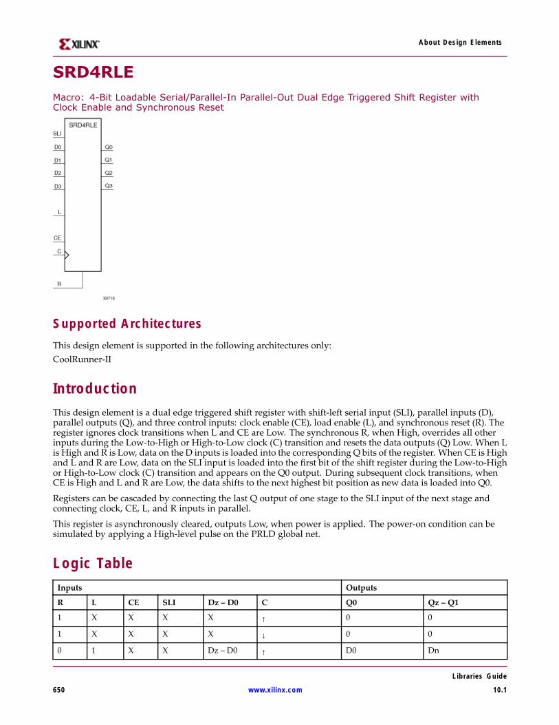
About Design Elements
SRD4RLEMacro: 4-Bit Loadable Serial/Parallel-In Parallel-Out Dual Edge Triggered Shift Register withClock Enable and Synchronous Reset
Supported ArchitecturesThis design element is supported in the following architectures only:CoolRunner-II
IntroductionThis design element is a dual edge triggered shift register with shift-left serial input (SLI), parallel inputs (D),parallel outputs (Q), and three control inputs: clock enable (CE), load enable (L), and synchronous reset (R). Theregister ignores clock transitions when L and CE are Low. The synchronous R, when High, overrides all otherinputs during the Low-to-High or High-to-Low clock (C) transition and resets the data outputs (Q) Low. When Lis High and R is Low, data on the D inputs is loaded into the corresponding Q bits of the register. When CE is Highand L and R are Low, data on the SLI input is loaded into the first bit of the shift register during the Low-to-Highor High-to-Low clock (C) transition and appears on the Q0 output. During subsequent clock transitions, whenCE is High and L and R are Low, the data shifts to the next highest bit position as new data is loaded into Q0.
Registers can be cascaded by connecting the last Q output of one stage to the SLI input of the next stage andconnecting clock, CE, L, and R inputs in parallel.
This register is asynchronously cleared, outputs Low, when power is applied. The power-on condition can besimulated by applying a High-level pulse on the PRLD global net.
Logic TableInputs Outputs
R L CE SLI Dz – D0 C Q0 Qz – Q1
1 X X X X ↑ 0 0
1 X X X X ↓ 0 0
0 1 X X Dz – D0 ↑ D0 Dn
Libraries Guide
650 www.xilinx.com 10.1

About Design Elements
Inputs Outputs
R L CE SLI Dz – D0 C Q0 Qz – Q1
0 1 X X Dz – D0 ↓ D0 Dn
0 0 1 SLI X ↑ SLI qn-1
0 0 1 SLI X ↓ SLI qn-1
0 0 0 X X X No Change No Change
z = bitwidth -1
Design Entry MethodThis design element is only for use in schematics.
For More Information• See the appropriate CPLD User Guide.
• See the appropriate CPLD Data Sheets.
Libraries Guide
10.1 www.xilinx.com 651

About Design Elements
SRD4RLED
Macro: 4-Bit Dual Edge Triggered Shift Register with Clock Enable and Synchronous Reset
Supported ArchitecturesThis design element is supported in the following architectures only:CoolRunner-II
IntroductionThis design element is a dual edge triggered shift register with shift-left (SLI) and shift-right (SRDI) serialinputs, parallel inputs (D), parallel outputs (Q), and four control inputs — clock enable (CE), load enable (L),shift left/right (LEFT), and synchronous reset (R). The register ignores clock transitions when CE and L areLow. The synchronous R, when High, overrides all other inputs during the Low-to-High or High-to-Lowclock (C) transition and resets the data outputs (Q) Low. When L is High and R is Low, the data on the Dinputs is loaded into the corresponding Q bits of the register. When CE is High and L and R are Low, data isshifted right or left, depending on the state of the LEFT input. If LEFT is High, data on SLI is loaded into Q0during the Low-to-High or High-to-Low clock transition and shifted left (to Q1, Q2, etc.) during subsequentclock transitions. If LEFT is Low, data on the SRDI is loaded into the last Q output during the Low-to-High orHigh-to-Low clock transition and shifted right during subsequent clock transitions. The logic table indicatesthe state of the Q outputs under all input conditions.
This register is asynchronously cleared, outputs Low, when power is applied. The power-on condition can besimulated by applying a High-level pulse on the PRLD global net.
Logic TableInputs Outputs
R L CE LEFT SLI SRDI D3 – D0 C Q0 Q3 Q2 – Q1
1 X X X X X X↑ ↑ 0 0 0
1 X X X X X X ↓ 0 0 0
0 1 X X X X D3 – D0 ↑ D0 D3 Dn
Libraries Guide
652 www.xilinx.com 10.1
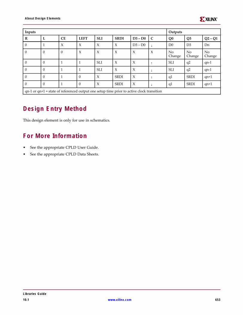
About Design Elements
Inputs Outputs
R L CE LEFT SLI SRDI D3 – D0 C Q0 Q3 Q2 – Q1
0 1 X X X X D3 – D0 ↓ D0 D3 Dn
0 0 0 X X X X X NoChange
NoChange
NoChange
0 0 1 1 SLI X X ↑ SLI q2 qn-1
0 0 1 1 SLI X X ↓ SLI q2 qn-1
0 0 1 0 X SRDI X ↑ q1 SRDI qn+1
0 0 1 0 X SRDI X ↓ q1 SRDI qn+1
qn-1 or qn+1 = state of referenced output one setup time prior to active clock transition
Design Entry MethodThis design element is only for use in schematics.
For More Information• See the appropriate CPLD User Guide.
• See the appropriate CPLD Data Sheets.
Libraries Guide
10.1 www.xilinx.com 653
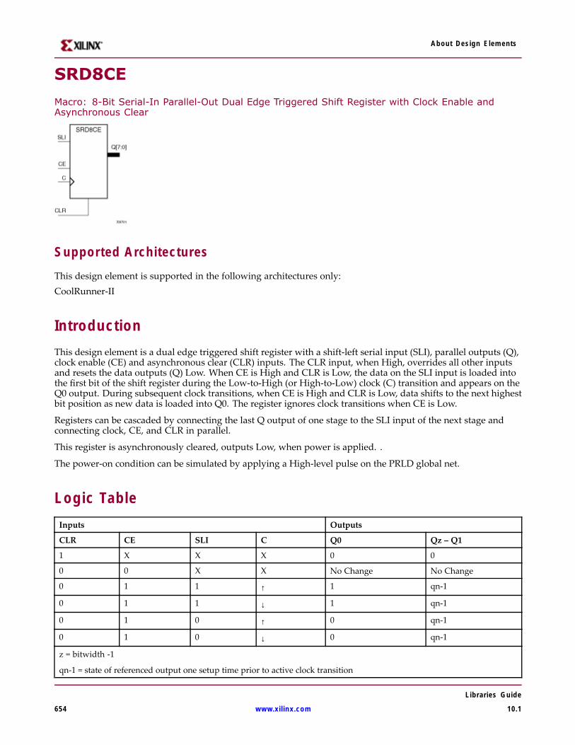
About Design Elements
SRD8CE
Macro: 8-Bit Serial-In Parallel-Out Dual Edge Triggered Shift Register with Clock Enable andAsynchronous Clear
Supported ArchitecturesThis design element is supported in the following architectures only:CoolRunner-II
IntroductionThis design element is a dual edge triggered shift register with a shift-left serial input (SLI), parallel outputs (Q),clock enable (CE) and asynchronous clear (CLR) inputs. The CLR input, when High, overrides all other inputsand resets the data outputs (Q) Low. When CE is High and CLR is Low, the data on the SLI input is loaded intothe first bit of the shift register during the Low-to-High (or High-to-Low) clock (C) transition and appears on theQ0 output. During subsequent clock transitions, when CE is High and CLR is Low, data shifts to the next highestbit position as new data is loaded into Q0. The register ignores clock transitions when CE is Low.
Registers can be cascaded by connecting the last Q output of one stage to the SLI input of the next stage andconnecting clock, CE, and CLR in parallel.
This register is asynchronously cleared, outputs Low, when power is applied. .
The power-on condition can be simulated by applying a High-level pulse on the PRLD global net.
Logic TableInputs Outputs
CLR CE SLI C Q0 Qz – Q1
1 X X X 0 0
0 0 X X No Change No Change
0 1 1 ↑ 1 qn-1
0 1 1 ↓ 1 qn-1
0 1 0 ↑ 0 qn-1
0 1 0 ↓ 0 qn-1
z = bitwidth -1
qn-1 = state of referenced output one setup time prior to active clock transition
Libraries Guide
654 www.xilinx.com 10.1

About Design Elements
Design Entry MethodThis design element is only for use in schematics.
For More Information• See the appropriate CPLD User Guide.
• See the appropriate CPLD Data Sheets.
Libraries Guide
10.1 www.xilinx.com 655

About Design Elements
SRD8CLE
Macro: 8-Bit Loadable Serial/Parallel-In Parallel-Out Dual Edge Triggered Shift Register withClock Enable and Asynchronous Clear
Supported ArchitecturesThis design element is supported in the following architectures only:CoolRunner-II
IntroductionThis design element is a dual edge triggered shift register with a shift-left serial input (SLI), parallel inputs (D),parallel outputs (Q), and three control inputs: clock enable (CE), load enable (L), and asynchronous clear (CLR).The register ignores clock transitions when L and CE are Low. The asynchronous CLR, when High, overrides allother inputs and resets the data outputs (Q) Low. When L is High and CLR is Low, data on the Dn – D0 inputs isloaded into the corresponding Qn – Q0 bits of the register. When CE is High and L and CLR are Low, data onthe SLI input is loaded into the first bit of the shift register during the Low-to-High (or High-to-Low) clock (C)transition and appears on the Q0 output. During subsequent clock transitions, when CE is High and L and CLRare Low, the data shifts to the next highest bit position as new data is loaded into Q0.
Registers can be cascaded by connecting the last Q output of one stage to the SLI input of the next stage andconnecting clock, CE, L, and CLR inputs in parallel.
This register is asynchronously cleared, outputs Low, when power is applied. The power-on condition can besimulated by applying a High-level pulse on the PRLD global net.
Logic TableInputs Outputs
CLR L CE SLI Dn – D0 C Q0 Qz – Q1
1 X X X X X 0 0
0 1 X X Dn – D0 ↑ D0 Dn
0 1 X X Dn – D0 ↓ D0 Dn
0 0 1 SLI X ↑ SLI qn-1
Libraries Guide
656 www.xilinx.com 10.1

About Design Elements
Inputs Outputs
CLR L CE SLI Dn – D0 C Q0 Qz – Q1
0 0 1 SLI X ↓ SLI qn-1
0 0 0 X X X No Change No Change
z = bitwidth -1
qn-1 = state of referenced output one setup time prior to active clock transition
Design Entry MethodThis design element is only for use in schematics.
For More Information• See the appropriate CPLD User Guide.
• See the appropriate CPLD Data Sheets.
Libraries Guide
10.1 www.xilinx.com 657

About Design Elements
SRD8CLEDMacro: 8-Bit Dual Edge Triggered Shift Register with Clock Enable and Asynchronous Clear
Supported ArchitecturesThis design element is supported in the following architectures only:CoolRunner-II
IntroductionThis design element is a dual edge triggered shift register with shift-left (SLI) and shift-right (SRI) serial inputs,parallel inputs (D), parallel outputs (Q), and four control inputs: clock enable (CE), load enable (L), shift left/right(LEFT), and asynchronous clear (CLR). The register ignores clock transitions when CE and L are Low. Theasynchronous clear, when High, overrides all other inputs and resets the data outputs (Qn) Low. When L is Highand CLR is Low, the data on the D inputs is loaded into the corresponding Q bits of the register. When CE isHigh and L and CLR are Low, data is shifted right or left, depending on the state of the LEFT input. If LEFT isHigh, data on the SLI is loaded into Q0 during the Low-to-High or High-to-Low clock transition and shifted leftduring subsequent clock transitions. If LEFT is Low, data on the SRI is loaded into the last Q output duringthe Low-to-High or High-to-Low clock transition and shifted right during subsequent clock transitions. Thelogic table indicates the state of the Q outputs under all input conditions.
This register is asynchronously cleared, outputs Low, when power is applied. The power-on condition can besimulated by applying a High-level pulse on the PRLD global net.
Logic TableInputs Outputs
CLR L CE LEFT SLI SRI D7 – D0 CLK Q0 Q7 Q6 – Q1
1 X X X X X X X 0 0 0
0 1 X X X X D7 – D0 ↑ D0 D7 Dn
0 1 X X X X D7 – D0 ↑ D0 D7 Dn
0 0 0 X X X X X NoChange
NoChange
NoChange
0 0 1 1 SLI X X ↑ SLI q6 qn-1
Libraries Guide
658 www.xilinx.com 10.1

About Design Elements
Inputs Outputs
CLR L CE LEFT SLI SRI D7 – D0 CLK Q0 Q7 Q6 – Q1
0 0 1 1 SLI X X ↓ SLI q6 qn-1
0 0 1 0 X SRI X ↑ q1 SRI qn+1
0 0 1 0 X SRI X ↓ q1 SRI qn+1
qn-1 or qn+1 = state of referenced output one setup time prior to active clock transition
Design Entry MethodThis design element is only for use in schematics.
For More Information• See the appropriate CPLD User Guide.
• See the appropriate CPLD Data Sheets.
Libraries Guide
10.1 www.xilinx.com 659

About Design Elements
SRD8REMacro: 8-Bit Serial-In Parallel-Out Dual Edge Triggered Shift Register with Clock Enable andSynchronous Reset
Supported ArchitecturesThis design element is supported in the following architectures only:CoolRunner-II
IntroductionThis design element is a dual edge triggered shift register with shift-left serial input (SLI), parallel outputs (Qn),clock enable (CE), and synchronous reset (R) inputs. The R input, when High, overrides all other inputs duringthe Low-to-High or High-to-Low clock (C) transition and resets the data outputs (Q) Low. When CE is Highand R is Low, the data on the SLI is loaded into the first bit of the shift register during the Low-to-High clock orHigh-to-Low (C) transition and appears on the Q0 output. During subsequent clock transitions, when CE isHigh and R is Low, data shifts to the next highest bit position as new data is loaded into Q0. The registerignores clock transitions when CE is Low.
Registers can be cascaded by connecting the last Q output of one stage to the SLI input of the next stage andconnecting clock, CE, and R in parallel.
This register is asynchronously cleared, outputs Low, when power is applied. The power-on condition can besimulated by applying a High-level pulse on the PRLD global net.
Logic TableInputs Outputs
R CE SLI C Q0 Qz – Q1
1 X X ↑ 0 0
1 X X ↓ 0 0
0 0 X X No Change No Change
0 1 1 ↑ 1 qn-1
0 1 1 ↓ 1 qn-1
0 1 0 ↑ 0 qn-1
0 1 0 ↓ 0 qn-1
z = bitwidth -1
qn-1 = state of referenced output one setup time prior to active clock transition
Libraries Guide
660 www.xilinx.com 10.1
About Design Elements
Design Entry MethodThis design element is only for use in schematics.
For More Information• See the appropriate CPLD User Guide.
• See the appropriate CPLD Data Sheets.
Libraries Guide
10.1 www.xilinx.com 661

About Design Elements
SRD8RLEMacro: 8-Bit Loadable Serial/Parallel-In Parallel-Out Dual Edge Triggered Shift Register withClock Enable and Synchronous Reset
Supported ArchitecturesThis design element is supported in the following architectures only:CoolRunner-II
IntroductionThis design element is a dual edge triggered shift register with shift-left serial input (SLI), parallel inputs (D),parallel outputs (Q), and three control inputs: clock enable (CE), load enable (L), and synchronous reset (R). Theregister ignores clock transitions when L and CE are Low. The synchronous R, when High, overrides all otherinputs during the Low-to-High or High-to-Low clock (C) transition and resets the data outputs (Q) Low. When Lis High and R is Low, data on the D inputs is loaded into the corresponding Q bits of the register. When CE is Highand L and R are Low, data on the SLI input is loaded into the first bit of the shift register during the Low-to-Highor High-to-Low clock (C) transition and appears on the Q0 output. During subsequent clock transitions, whenCE is High and L and R are Low, the data shifts to the next highest bit position as new data is loaded into Q0.
Registers can be cascaded by connecting the last Q output of one stage to the SLI input of the next stage andconnecting clock, CE, L, and R inputs in parallel.
This register is asynchronously cleared, outputs Low, when power is applied. The power-on condition can besimulated by applying a High-level pulse on the PRLD global net.
Logic TableInputs Outputs
R L CE SLI Dz – D0 C Q0 Qz – Q1
1 X X X X ↑ 0 0
1 X X X X ↓ 0 0
0 1 X X Dz – D0 ↑ D0 Dn
0 1 X X Dz – D0 ↓ D0 Dn
0 0 1 SLI X ↑ SLI qn-1
Libraries Guide
662 www.xilinx.com 10.1
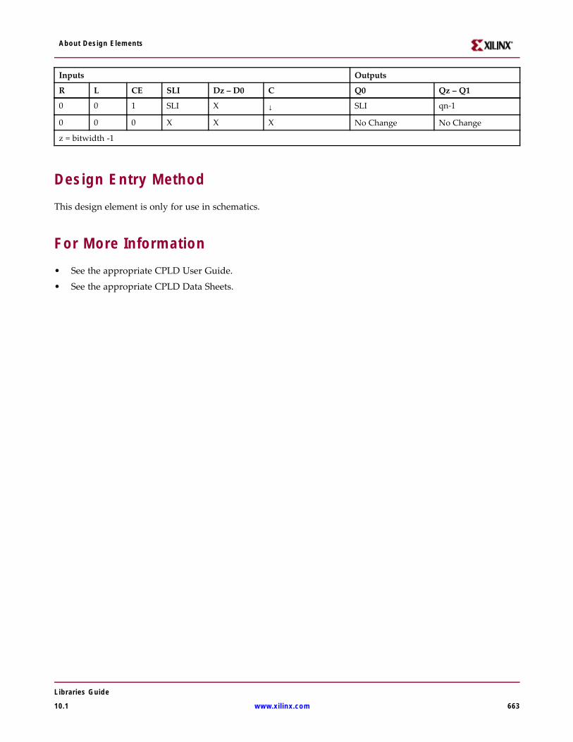
About Design Elements
Inputs Outputs
R L CE SLI Dz – D0 C Q0 Qz – Q1
0 0 1 SLI X ↓ SLI qn-1
0 0 0 X X X No Change No Change
z = bitwidth -1
Design Entry MethodThis design element is only for use in schematics.
For More Information• See the appropriate CPLD User Guide.
• See the appropriate CPLD Data Sheets.
Libraries Guide
10.1 www.xilinx.com 663

About Design Elements
SRD8RLED
Macro: 8-Bit Dual Edge Triggered Shift Register with Clock Enable and Synchronous Reset
Supported ArchitecturesThis design element is supported in the following architectures only:CoolRunner-II
IntroductionThis design element is a dual edge triggered shift register with shift-left (SLI) and shift-right (SRDI) serialinputs, parallel inputs (D), parallel outputs (Q), and four control inputs — clock enable (CE), load enable (L),shift left/right (LEFT), and synchronous reset (R). The register ignores clock transitions when CE and L areLow. The synchronous R, when High, overrides all other inputs during the Low-to-High or High-to-Lowclock (C) transition and resets the data outputs (Q) Low. When L is High and R is Low, the data on the Dinputs is loaded into the corresponding Q bits of the register. When CE is High and L and R are Low, data isshifted right or left, depending on the state of the LEFT input. If LEFT is High, data on SLI is loaded into Q0during the Low-to-High or High-to-Low clock transition and shifted left (to Q1, Q2, etc.) during subsequentclock transitions. If LEFT is Low, data on the SRDI is loaded into the last Q output during the Low-to-High orHigh-to-Low clock transition and shifted right during subsequent clock transitions. The logic table indicatesthe state of the Q outputs under all input conditions.
This register is asynchronously cleared, outputs Low, when power is applied. The power-on condition can besimulated by applying a High-level pulse on the PRLD global net.
Logic TableInputs Outputs
R L CE LEFT SLI SRDI D7– D0 C Q0 Q7 Q6 – Q1
1 X X X X X X ↑ 0 0 0
1 X X X X X X ↓ 0 0 0
0 1 X X X X D7 – D0 ↑ D0 D7 Dn
0 1 X X X X D7 – D0 ↓ D0 D7 Dn
Libraries Guide
664 www.xilinx.com 10.1

About Design Elements
Inputs Outputs
R L CE LEFT SLI SRDI D7– D0 C Q0 Q7 Q6 – Q1
0 0 0 X X X X X NoChange
NoChange
NoChange
0 0 1 1 SLI X X ↑ SLI q6 qn-1
0 0 1 1 SLI X X ↓ SLI q6 qn-1
0 0 1 0 X SRDI X ↑ q1 SRDI qn+1
0 0 1 0 X SRDI X ↓ q1 SRDI qn+1
qn-1 or qn+1 = state of referenced output one setup time prior to active clock transition
Design Entry MethodThis design element is only for use in schematics.
For More Information• See the appropriate CPLD User Guide.
• See the appropriate CPLD Data Sheets.
Libraries Guide
10.1 www.xilinx.com 665

About Design Elements
VCC
Primitive: VCC-Connection Signal Tag
Supported Architectures
This design element is supported in the following architectures only:
• XC9500XL
• CoolRunner XPLA3
• CoolRunner-II
IntroductionThis design element serves as a signal tag, or parameter, that forces a net or input function to a logic High level.A net tied to this element cannot have any other source.
When the placement and routing software encounters a net or input function tied to this element, it removes anylogic that is disabled by the Vcc signal, which is only implemented when the disabled logic cannot be removed.
Design Entry MethodThis design element is only for use in schematics.
For More Information• See the appropriate CPLD User Guide.
• See the appropriate CPLD Data Sheets.
Libraries Guide
666 www.xilinx.com 10.1

About Design Elements
XNOR2
Primitive: 2-Input XNOR Gate with Non-Inverted Inputs
Supported Architectures
This design element is supported in the following architectures only:
• XC9500XL
• CoolRunner XPLA3
• CoolRunner-II
IntroductionXNOR functions of up to nine inputs are available. All inputs are non-inverting. Because each input uses a CLBresource, replace functions with unused inputs with functions having the necessary number of inputs.
Logic TableInput Output
I0 ... Iz O
Odd number of 1 0
Even number of 1 1
Design Entry MethodThis design element is only for use in schematics.
For More Information• See the appropriate CPLD User Guide.
• See the appropriate CPLD Data Sheets.
Libraries Guide
10.1 www.xilinx.com 667

About Design Elements
XNOR3
Primitive: 3-Input XNOR Gate with Non-Inverted Inputs
Supported Architectures
This design element is supported in the following architectures only:
• XC9500XL
• CoolRunner XPLA3
• CoolRunner-II
IntroductionXNOR functions of up to nine inputs are available. All inputs are non-inverting. Because each input uses a CLBresource, replace functions with unused inputs with functions having the necessary number of inputs.
Logic TableInput Output
I0 ... Iz O
Odd number of 1 0
Even number of 1 1
Design Entry MethodThis design element is only for use in schematics.
For More Information• See the appropriate CPLD User Guide.
• See the appropriate CPLD Data Sheets.
Libraries Guide
668 www.xilinx.com 10.1

About Design Elements
XNOR4
Primitive: 4-Input XNOR Gate with Non-Inverted Inputs
Supported Architectures
This design element is supported in the following architectures only:
• XC9500XL
• CoolRunner XPLA3
• CoolRunner-II
IntroductionXNOR functions of up to nine inputs are available. All inputs are non-inverting. Because each input uses a CLBresource, replace functions with unused inputs with functions having the necessary number of inputs.
Logic TableInput Output
I0 ... Iz O
Odd number of 1 0
Even number of 1 1
Design Entry MethodThis design element is only for use in schematics.
For More Information• See the appropriate CPLD User Guide.
• See the appropriate CPLD Data Sheets.
Libraries Guide
10.1 www.xilinx.com 669

About Design Elements
XNOR5
Primitive: 5-Input XNOR Gate with Non-Inverted Inputs
Supported Architectures
This design element is supported in the following architectures only:
• XC9500XL
• CoolRunner XPLA3
• CoolRunner-II
IntroductionXNOR functions of up to nine inputs are available. All inputs are non-inverting. Because each input uses a CLBresource, replace functions with unused inputs with functions having the necessary number of inputs.
Logic TableInput Output
I0 ... Iz O
Odd number of 1 0
Even number of 1 1
Design Entry MethodThis design element is only for use in schematics.
For More Information• See the appropriate CPLD User Guide.
• See the appropriate CPLD Data Sheets.
Libraries Guide
670 www.xilinx.com 10.1

About Design Elements
XNOR6
Macro: 6-Input XNOR Gate with Non-Inverted Inputs
Supported Architectures
This design element is supported in the following architectures only:
• XC9500XL
• CoolRunner XPLA3
• CoolRunner-II
IntroductionXNOR functions of up to nine inputs are available. All inputs are non-inverting. Because each input uses a CLBresource, replace functions with unused inputs with functions having the necessary number of inputs.
Logic TableInput Output
I0 ... Iz O
Odd number of 1 0
Even number of 1 1
Design Entry MethodThis design element is only for use in schematics.
For More Information• See the appropriate CPLD User Guide.
• See the appropriate CPLD Data Sheets.
Libraries Guide
10.1 www.xilinx.com 671

About Design Elements
XNOR7
Macro: 7-Input XNOR Gate with Non-Inverted Inputs
Supported Architectures
This design element is supported in the following architectures only:
• XC9500XL
• CoolRunner XPLA3
• CoolRunner-II
IntroductionXNOR functions of up to nine inputs are available. All inputs are non-inverting. Because each input uses a CLBresource, replace functions with unused inputs with functions having the necessary number of inputs.
Logic TableInput Output
I0 ... Iz O
Odd number of 1 0
Even number of 1 1
Design Entry MethodThis design element is only for use in schematics.
For More Information• See the appropriate CPLD User Guide.
• See the appropriate CPLD Data Sheets.
Libraries Guide
672 www.xilinx.com 10.1

About Design Elements
XNOR8
Macro: 8-Input XNOR Gate with Non-Inverted Inputs
Supported Architectures
This design element is supported in the following architectures only:
• XC9500XL
• CoolRunner XPLA3
• CoolRunner-II
IntroductionXNOR functions of up to nine inputs are available. All inputs are non-inverting. Because each input uses a CLBresource, replace functions with unused inputs with functions having the necessary number of inputs.
Logic TableInput Output
I0 ... Iz O
Odd number of 1 0
Even number of 1 1
Design Entry MethodThis design element is only for use in schematics.
For More Information• See the appropriate CPLD User Guide.
• See the appropriate CPLD Data Sheets.
Libraries Guide
10.1 www.xilinx.com 673

About Design Elements
XNOR9
Macro: 9-Input XNOR Gate with Non-Inverted Inputs
Supported Architectures
This design element is supported in the following architectures only:
• XC9500XL
• CoolRunner XPLA3
• CoolRunner-II
IntroductionXNOR functions of up to nine inputs are available. All inputs are non-inverting. Because each input uses a CLBresource, replace functions with unused inputs with functions having the necessary number of inputs.
Logic TableInput Output
I0 ... Iz O
Odd number of 1 0
Even number of 1 1
Design Entry MethodThis design element is only for use in schematics.
For More Information• See the appropriate CPLD User Guide.
• See the appropriate CPLD Data Sheets.
Libraries Guide
674 www.xilinx.com 10.1

About Design Elements
XOR2
Primitive: 2-Input XOR Gate with Non-Inverted Inputs
Supported Architectures
This design element is supported in the following architectures only:
• XC9500XL
• CoolRunner XPLA3
• CoolRunner-II
IntroductionXOR functions of up to nine inputs are available. All inputs are non-inverting. Because each input uses a CLBresource, replace functions with unused inputs with functions having the necessary number of inputs.
Design Entry MethodThis design element is only for use in schematics.
For More Information• See the appropriate CPLD User Guide.
• See the appropriate CPLD Data Sheets.
Libraries Guide
10.1 www.xilinx.com 675

About Design Elements
XOR3
Primitive: 3-Input XOR Gate with Non-Inverted Inputs
Supported Architectures
This design element is supported in the following architectures only:
• XC9500XL
• CoolRunner XPLA3
• CoolRunner-II
IntroductionXOR functions of up to nine inputs are available. All inputs are non-inverting. Because each input uses a CLBresource, replace functions with unused inputs with functions having the necessary number of inputs.
Design Entry MethodThis design element is only for use in schematics.
For More Information• See the appropriate CPLD User Guide.
• See the appropriate CPLD Data Sheets.
Libraries Guide
676 www.xilinx.com 10.1

About Design Elements
XOR4
Primitive: 4-Input XOR Gate with Non-Inverted Inputs
Supported Architectures
This design element is supported in the following architectures only:
• XC9500XL
• CoolRunner XPLA3
• CoolRunner-II
IntroductionXOR functions of up to nine inputs are available. All inputs are non-inverting. Because each input uses a CLBresource, replace functions with unused inputs with functions having the necessary number of inputs.
Design Entry MethodThis design element is only for use in schematics.
For More Information• See the appropriate CPLD User Guide.
• See the appropriate CPLD Data Sheets.
Libraries Guide
10.1 www.xilinx.com 677
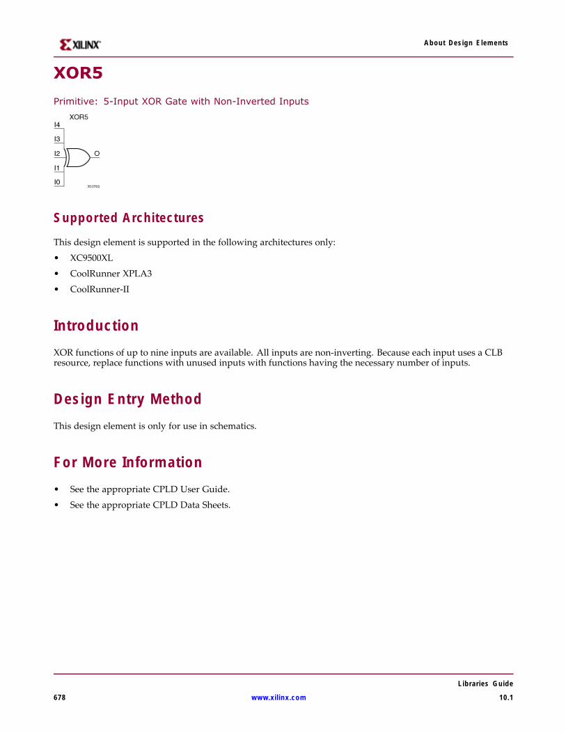
About Design Elements
XOR5
Primitive: 5-Input XOR Gate with Non-Inverted Inputs
Supported Architectures
This design element is supported in the following architectures only:
• XC9500XL
• CoolRunner XPLA3
• CoolRunner-II
IntroductionXOR functions of up to nine inputs are available. All inputs are non-inverting. Because each input uses a CLBresource, replace functions with unused inputs with functions having the necessary number of inputs.
Design Entry MethodThis design element is only for use in schematics.
For More Information• See the appropriate CPLD User Guide.
• See the appropriate CPLD Data Sheets.
Libraries Guide
678 www.xilinx.com 10.1

About Design Elements
XOR6
Macro: 6-Input XOR Gate with Non-Inverted Inputs
Supported Architectures
This design element is supported in the following architectures only:
• XC9500XL
• CoolRunner XPLA3
• CoolRunner-II
IntroductionXOR functions of up to nine inputs are available. All inputs are non-inverting. Because each input uses a CLBresource, replace functions with unused inputs with functions having the necessary number of inputs.
Design Entry MethodThis design element is only for use in schematics.
For More Information• See the appropriate CPLD User Guide.
• See the appropriate CPLD Data Sheets.
Libraries Guide
10.1 www.xilinx.com 679
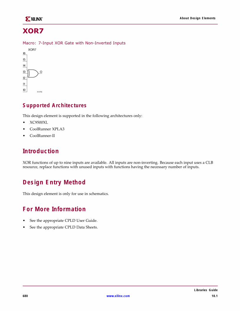
About Design Elements
XOR7
Macro: 7-Input XOR Gate with Non-Inverted Inputs
Supported Architectures
This design element is supported in the following architectures only:
• XC9500XL
• CoolRunner XPLA3
• CoolRunner-II
IntroductionXOR functions of up to nine inputs are available. All inputs are non-inverting. Because each input uses a CLBresource, replace functions with unused inputs with functions having the necessary number of inputs.
Design Entry MethodThis design element is only for use in schematics.
For More Information• See the appropriate CPLD User Guide.
• See the appropriate CPLD Data Sheets.
Libraries Guide
680 www.xilinx.com 10.1

About Design Elements
XOR8
Macro: 8-Input XOR Gate with Non-Inverted Inputs
Supported Architectures
This design element is supported in the following architectures only:
• XC9500XL
• CoolRunner XPLA3
• CoolRunner-II
IntroductionXOR functions of up to nine inputs are available. All inputs are non-inverting. Because each input uses a CLBresource, replace functions with unused inputs with functions having the necessary number of inputs.
Design Entry MethodThis design element is only for use in schematics.
For More Information• See the appropriate CPLD User Guide.
• See the appropriate CPLD Data Sheets.
Libraries Guide
10.1 www.xilinx.com 681

About Design Elements
XOR9
Macro: 9-Input XOR Gate with Non-Inverted Inputs
Supported Architectures
This design element is supported in the following architectures only:
• XC9500XL
• CoolRunner XPLA3
• CoolRunner-II
IntroductionXOR functions of up to nine inputs are available. All inputs are non-inverting. Because each input uses a CLBresource, replace functions with unused inputs with functions having the necessary number of inputs.
Design Entry MethodThis design element is only for use in schematics.
For More Information• See the appropriate CPLD User Guide.
• See the appropriate CPLD Data Sheets.
Libraries Guide
682 www.xilinx.com 10.1