workshop nanoscience on the tip
TRANSCRIPT
WORKSHOP Nanoscience on the Tip
2007LaboratoryProgram/rev 13
LAB UNIT 1: Introduction to Scanning Force Microscopy and Dip-Pen Nanolithography
Specific Assignment: Introduction to Scanning Force Microscopy (SFM) and Dip-Pen Nanolithography (DPN) Gold Etching with DPN-generated Templates and Contact Mode Imaging
Objective The student will become familiar with contact mode
Scanning Force Microscopy (SFM) as an imaging technique, and be introduced with Dip-Pen Nanolithography (DPN).
Outcome At the end of this lab, you will be familiar with the basic
principles and techniques of contact mode SFM and DPN, and you will obtain some familiarity with script-based control of the NanoSurf SFM.
Synopsis In this lab, you will use DPN to generate nanoscale resists
for gold etching, and you will subsequently use SFM to image the patterned structures in contact mode.
Materials 16-mercaptohexadecanoic acid, gold films on silicon oxide
wafers, and gold etchant solution (thiourea and ferric nitrate) Techniques Contact mode SFM and DPN
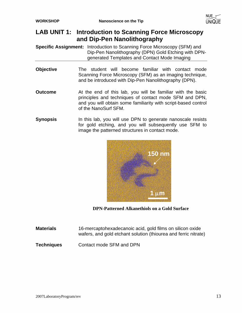
1 μm
150 nm
DPN-Patterned Alkanethiols on a Gold Surface
LAB UNIT 1
14
Table of Contents
1. Assignment ......................................................................................................................... 15 2. Quiz ...................................................................................................................................... 16
2.1 Short Answers ..................................................................................................... 16 3. Experimental Assignment ................................................................................................. 18
3.1 Goal ..................................................................................................................... 18 3.2 Safety .................................................................................................................. 18 3.3 Instrumental Setup .............................................................................................. 19 3.4 Materials ............................................................................................................. 19 3.5 Experimental Procedure ...................................................................................... 20 3.6 Easy Scan 2 AFM system components and tools ............................................... 25 3.7 Easy Scan 2 AFM System Standard Operational Procedure .............................. 27 3.7.1 Startup Procedure ............................................................................................. 27 3.7.2 Shutdown Procedure ........................................................................................ 32
4. Scanning Probe Microscopy and Dip-Pen Nanolithography ......................................... 33 4.1 Historic Perspectives ........................................................................................... 33 4.2 Scanning Force Microscopy (SFM) .................................................................... 34 4.2.1. Contact Mode .................................................................................................. 34 4.2.2. AC Mode Imaging .......................................................................................... 35 4.2.3. Applied Force: Cantilever Deflection and Hooke’s Law ............................... 35 4.2.4. SFM Tips ........................................................................................................ 36 4.3 Dip-Pen Nanolithography (DPN) ....................................................................... 39
References .............................................................................................................................. 40
Scanning Force Microscopy & Dip-Pen Nanolithography
2007LaboratoryProgram/rev 15
1. Assignment In this lab, you will use the Scanning Force Microscope (SFM), also known as Atomic Force Microscope (AFM), as both an imaging tool, and as a writing tool. As an imaging tool, you will use the most basic SFM imaging method: contact mode imaging. You will use the SFM tip as a nanoscale writing tool to deliver chemical “inks” to a surface very much like a nanoscale fountain pen. These inks will serve as etch resists that you will develop into patterns that can be imaged using contact mode SFM. The unpatterned region of gold surface will be etched in a solution of thiourea and ferric nitrate. We will then use SFM in contact mode to image the resulting nanostructures. The steps are outlined here:
1. (pre-lab) Read the Material Safety Data Sheets (MSDS) of all chemicals used in this lab
2. (pre-lab) Read background information of Scanning Probe Microscopy and Dip-Pen Nanolithography in section 4
3. Take the quiz on your theoretical understanding in section 2 4. Generate mercaptohexadecanoic acid patterns on gold surface as negative resists
for gold etching using dip-pen nanolithography 5. Etch the unpatterned gold region to generate nanostructures using wet chemistry 6. Image the resulting gold patterns with atomic force microscopy in contact mode 7. Perform cross-section analysis on the topography of the structures to determine
their diameter and height 8. Compare the feature size as a function of DPN dwell time 9. Compile a report to summarize your findings from this lab. Your report should include the following with a brief discussion:
• Topography image showing your DPN-generated structures with scale bar • Cross-section profile of your structures • Dimensions of your structures (report average diameter and height with
standard deviation) • Compare diameters with those predicted from eq. (4) and plot of dot sizes
vs. dwell time of DPN Chemical Hazards: See Experimental Assignment (section 3)
LAB UNIT 1
16
2. Quiz
2.1 Short Answers
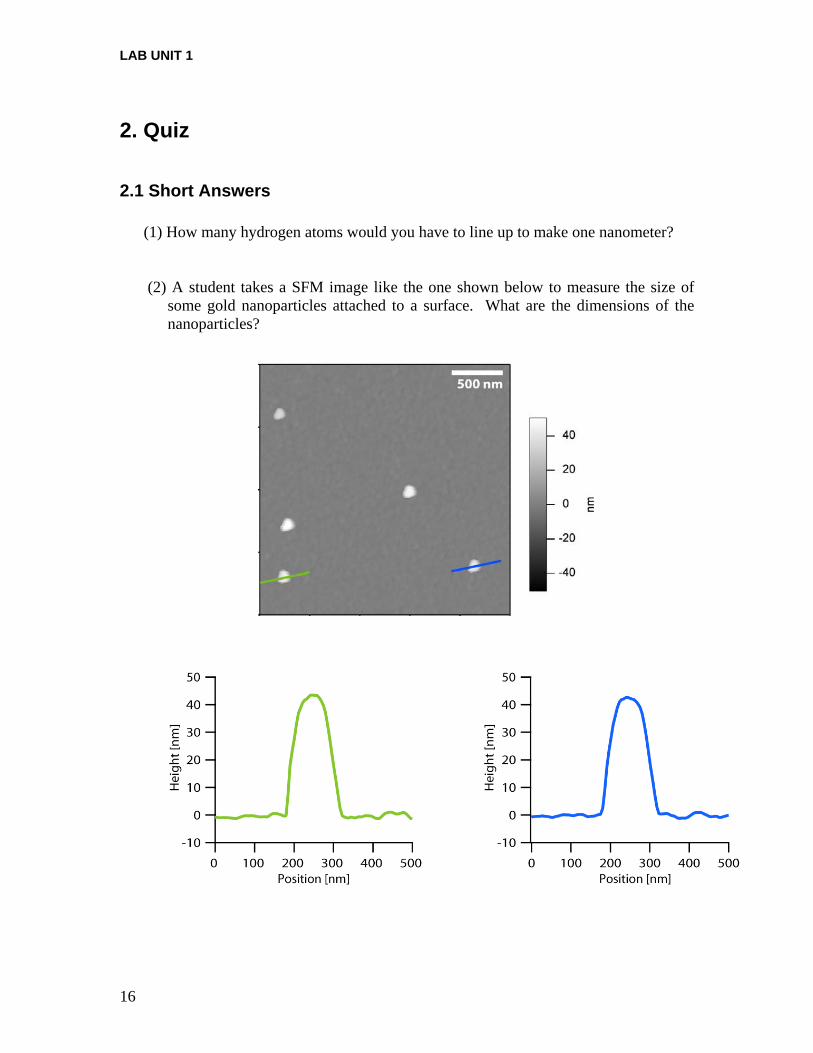
(1) How many hydrogen atoms would you have to line up to make one nanometer? (2) A student takes a SFM image like the one shown below to measure the size of
some gold nanoparticles attached to a surface. What are the dimensions of the nanoparticles?

Scanning Force Microscopy & Dip-Pen Nanolithography
2007LaboratoryProgram/rev 17
(3) A student takes an SFM like the one shown below. Explain what has gone wrong.
(4) A) What is the force constant of the cantilevers you will be using in this lab? B) How much force does it take to deflect such a cantilever by 1nm? C) Provide an order of magnitude estimate of how much force is needed to break
a covalent bond (remember typical ~1 Angstrom long, ~80 kcal/mol). D) Calculate the force that a 1 mW beam of 830 nm photons exerts on a mirror. (5) Using the same SFM cantilever as in problem (4) the deflection set point is set to
10 nN. A) How far is the cantilever deflected from equilibrium? B) What is the pressure beneath the SFM tip if the contact area is 30 nm in
diameter? (6) How does the SFM scan the tip across the surface? (7) If you are scanning an area of 80 μm by 80 μm with 512 lines and 512 points per
line, what is the resolution of your image (specify in both μm and nm)?
LAB UNIT 1
18
3. Experimental Assignment 3.1 Goal At the end of this lab, you should understand the concept and operation of SFM contact mode and able to use DPN to create nanostructures. Specifically perform the following:
(1) Use DPN to generate patterns of thiols on gold surfaces to act as resists in gold etching
(2) Create a few nanometers tall gold structures from the DPN-generated patterns (3) Use SFM in contact mode to obtain topography of the generated gold structures
3.2 Safety - Wear safety glasses and gloves - Use extreme cautious when handling chemicals and be sure you have read the
MSDS - Refer to the General rules in the SFM lab
Chemical Hazards: You will be using a solution of thiourea and ferric nitrate to etch gold films in this lab. This solution is a strong oxidizer. It is toxic and a carcinogen. Not only can it burn your skin, but it can cause a fire if it is brought into contact with combustible material. The solution should be stored away from heat, strong acids, strong bases, and organic materials. Wear goggles, gloves and lab coats when handling the thiourea solutions. Never generate or handle more than 10 mL of etching solution. If you spill the solution on your skin, you should flush the area with copious amounts of water for at least 15 minutes and remove the contaminated clothing and shoes. After that you should contact a physician. If you spill the solution on the bench you should ask the TA for assistance. The area should be evacuated immediately. You should wear a self-contained breathing apparatus, a pair of rubber boots, and heavy rubber gloves to clean. The spills should be absorbed on sand or vermiculite and be placed in a closed container for proper disposal. After the spills have been picked up, you should wash the spilled area and ventilate the area. Always handle the solutions in a well-ventilated area. The solution is highly toxic to aquatic species and must not be poured down the drain. It must be properly disposed at the designated chemical waste jar. Warning: The AFM contains a Class 1 laser (830 nm wavelength). Although class 1 lasers are deemed safe for brief exposure, you should NOT look directly into the laser beam behind the cantilever alignment chip. The laser is infrared, meaning your blink reflex will not protect you.
Scanning Force Microscopy & Dip-Pen Nanolithography
2007LaboratoryProgram/rev 19
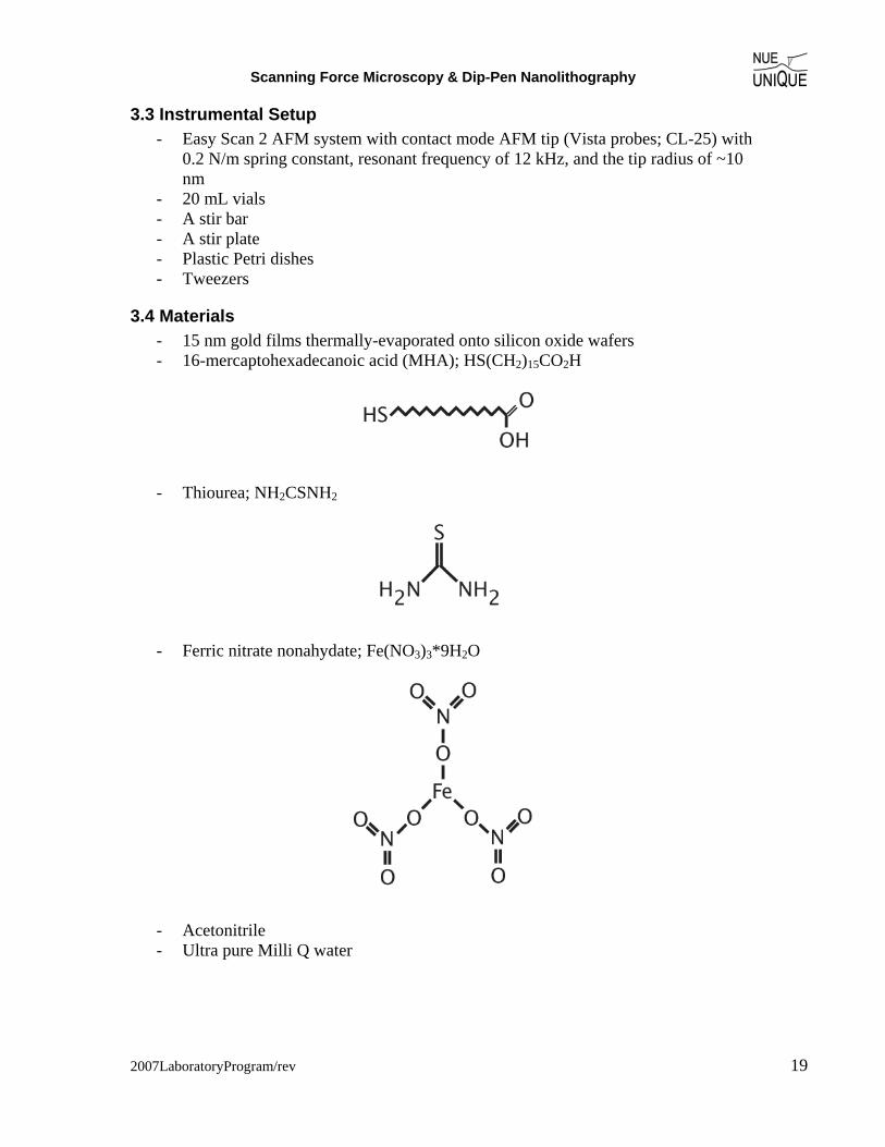
3.3 Instrumental Setup - Easy Scan 2 AFM system with contact mode AFM tip (Vista probes; CL-25) with
0.2 N/m spring constant, resonant frequency of 12 kHz, and the tip radius of ~10 nm
- 20 mL vials - A stir bar - A stir plate - Plastic Petri dishes - Tweezers
3.4 Materials - 15 nm gold films thermally-evaporated onto silicon oxide wafers - 16-mercaptohexadecanoic acid (MHA); HS(CH2)15CO2H
- Thiourea; NH2CSNH2
- Ferric nitrate nonahydate; Fe(NO3)3*9H2O
- Acetonitrile - Ultra pure Milli Q water
LAB UNIT 1
20
3.5 Experimental Procedure Read the instructions below carefully and follow them closely. If you are uncertain
about anything, please consult your TA first.
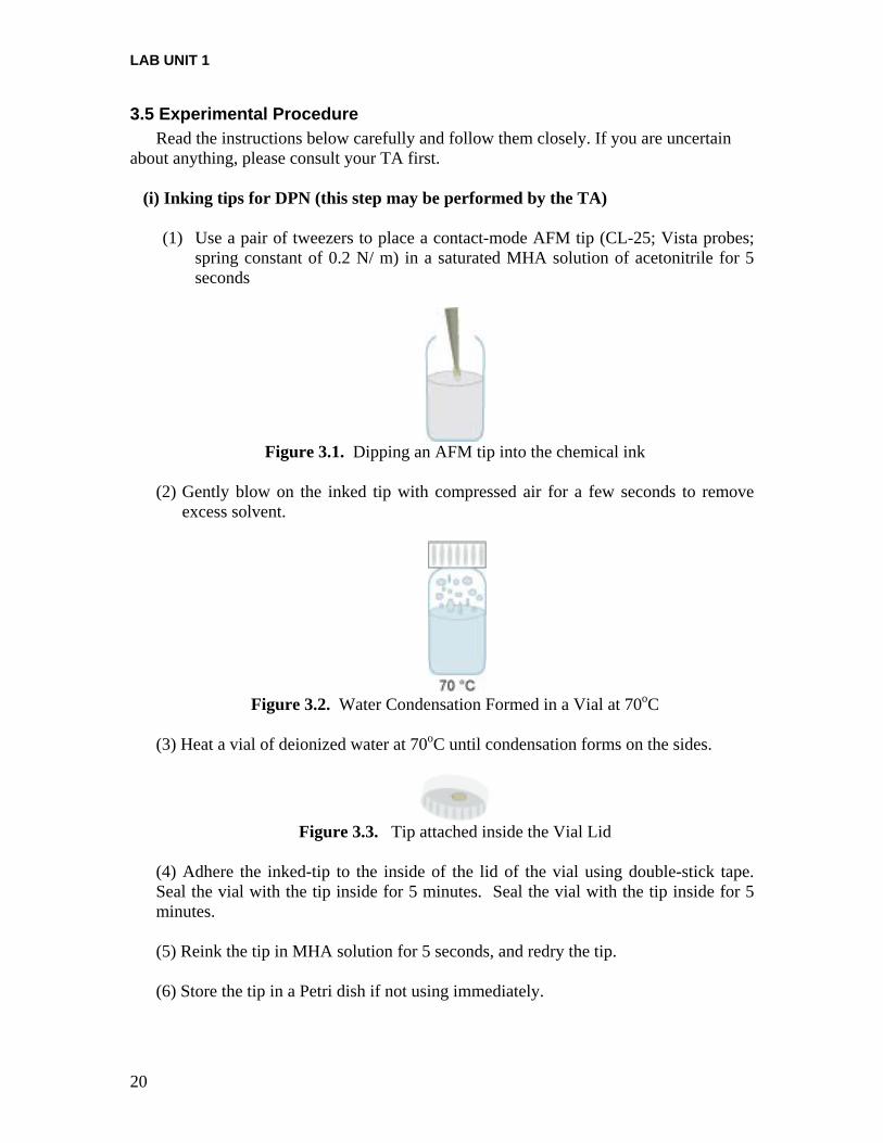
(i) Inking tips for DPN (this step may be performed by the TA)
(1) Use a pair of tweezers to place a contact-mode AFM tip (CL-25; Vista probes; spring constant of 0.2 N/ m) in a saturated MHA solution of acetonitrile for 5 seconds
Figure 3.1. Dipping an AFM tip into the chemical ink
(2) Gently blow on the inked tip with compressed air for a few seconds to remove
excess solvent.
Figure 3.2. Water Condensation Formed in a Vial at 70oC
(3) Heat a vial of deionized water at 70oC until condensation forms on the sides.
Figure 3.3. Tip attached inside the Vial Lid
(4) Adhere the inked-tip to the inside of the lid of the vial using double-stick tape. Seal the vial with the tip inside for 5 minutes. Seal the vial with the tip inside for 5 minutes. (5) Reink the tip in MHA solution for 5 seconds, and redry the tip. (6) Store the tip in a Petri dish if not using immediately.
Scanning Force Microscopy & Dip-Pen Nanolithography
2007LaboratoryProgram/rev 21
(ii) Preparation of the experiment
(1) Scratch an alignment mark by gently scratching a “4” on a gold substrate using a razor blade or the tip of your tweezers. BE GENTLE, you only want to lightly scratch the gold, if you press to hard you will scratch into the silicon oxide layer and create lots of dust which will make the subsequent steps more difficult.
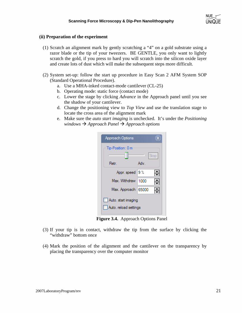
(2) System set-up: follow the start up procedure in Easy Scan 2 AFM System SOP
(Standard Operational Procedure). a. Use a MHA-inked contact-mode cantilever (CL-25) b. Operating mode: static force (contact mode) c. Lower the stage by clicking Advance in the Approach panel until you see
the shadow of your cantilever. d. Change the positioning view to Top View and use the translation stage to
locate the cross area of the alignment mark e. Make sure the auto start imaging is unchecked. It’s under the Positioning
windows Approach Panel Approach options
Figure 3.4. Approach Options Panel
(3) If your tip is in contact, withdraw the tip from the surface by clicking the
“withdraw” bottom once (4) Mark the position of the alignment and the cantilever on the transparency by
placing the transparency over the computer monitor

LAB UNIT 1
22
(iii) Dip-Pen Nanolithography
The goal of this section is to utilize a lithography program to write with AFM a series of dots of different sizes by varying the dwell time, and to compare your data against a theoretical prediction (see background information). The lithography program is written in the script function of the easyScan 2 software.
(1) Open the lithography program by clicking a. Script on the tool bar b. Script Editor c. Load the file from the desktop, DPN.vbs d. The Script will write four 5 × 5 grids of dots, each with a different dwell
time, as shown in Fig. 3.5. The dwell times are stored in an array called, appropriately, diptimes. Change these four diptimes to four different times of your choosing, between 1 and 20 seconds.
Figure 3.5. DPN Patterns
(2) Running DPN a. Make sure the tip is within approaching distance to the surface b. Click run on the Script Editor c. Wait until the script finishes running. A dialog box will pop up that says
“Done writing!”
(3) Removing patterned substrates a. Retract the cantilever by first clicking on the withdraw (in the Approach
panel). When the tip stops moving, click and hold the Retract bottom until there is enough clearance between the tip and the substrate.
b. Remove the AFM scan head c. Remove the gold substrate

Scanning Force Microscopy & Dip-Pen Nanolithography
2007LaboratoryProgram/rev 23
(iv) Gold etching
In this section, we will use the DPN-generated patterns from the previous section as resists in the gold etching to create gold structures. The unpatterned gold regions will be etched first and faster than the MHA-patterned gold areas.
(1) Make a 20 mM ferric nitrate and 30 mM thiourea in DI water and mix the solution well
(2) Pour the solution into a Petri dish with a stir bar on a stir plate (3) Adjust the stir plate to about 200 rpm for gentle mixing
(4) Place the patterned-gold substrate in the solution for 1 minute
(5) Rinse the substrate with DI water for 5 seconds
(6) Blow the substrate with nitrogen
(7) Repeat steps (4) to (6)
(v) AFM imaging of the generated nanostructures
Finally, we use AFM contact mode to image the generated gold structures, determine the diameters of the structures, and perform the cross-section analysis of the structures from the topography images.
(1) Place the substrate on the AFM translation stage (2) Place the AFM scan head on the stage
(3) Follow the Easy Scan 2 AFM System SOP Startup Procedure to approach the tip
(4) Withdraw the tip from the surface by clicking the “withdraw” bottom once
(5) Use the marked transparency from before to locate your patterned region by
adjusting the translation stage
(6) Approach the tip and scan a 110 micron by 110 micron area following the instruction step 9 to 11 on the Easy Scan 2 AFM System SOP Startup Procedure
(7) Save the image by clicking photo and wait until the scan has reached the end
LAB UNIT 1
24
(8) Zoom-in to your DPN-patterned structures by clicking zoom in the imaging bar and use mouse cursor to define the interested area. Then, click zoom on the left side Tool results panel.
(9) Scan the selected area (10)Save the image (11) Process image and perform cross-section analysis using the options under the Tools. Keep in mind that you want to obtain the following information,
• Cross-section profile of your structures • Dimensions of your structures (report average diameter and height with
standard deviation) • Compare diameters with those predicted from eq. (4) and plot of dot sizes
vs. dwell time of DPN
(vi) AFM shut down
(1) Follow the Easy Scan 2 AFM System SOP Shutdown Procedure (2) Dispose all of the chemical waste properly
Scanning Force Microscopy & Dip-Pen Nanolithography
2007LaboratoryProgram/rev 25
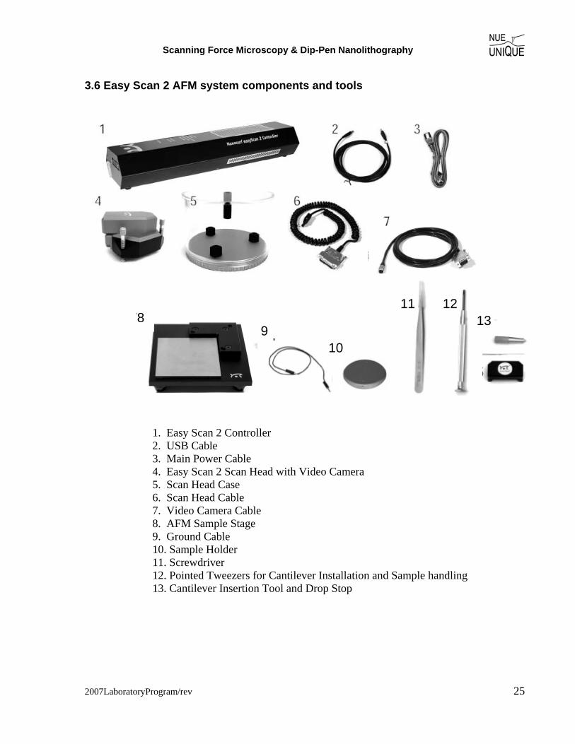
3.6 Easy Scan 2 AFM system components and tools
1. Easy Scan 2 Controller 2. USB Cable 3. Main Power Cable 4. Easy Scan 2 Scan Head with Video Camera 5. Scan Head Case 6. Scan Head Cable 7. Video Camera Cable 8. AFM Sample Stage 9. Ground Cable 10. Sample Holder 11. Screwdriver 12. Pointed Tweezers for Cantilever Installation and Sample handling 13. Cantilever Insertion Tool and Drop Stop
8 9
10
11 12 13
LAB UNIT 1
26
Scanning Force Microscopy & Dip-Pen Nanolithography
2007LaboratoryProgram/rev 27
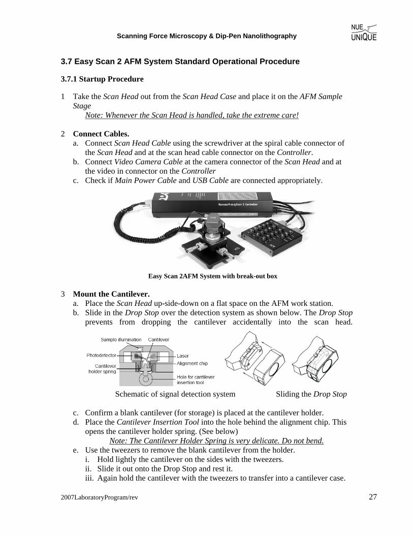
3.7 Easy Scan 2 AFM System Standard Operational Procedure
3.7.1 Startup Procedure
1 Take the Scan Head out from the Scan Head Case and place it on the AFM Sample Stage
Note: Whenever the Scan Head is handled, take the extreme care!
2 Connect Cables. a. Connect Scan Head Cable using the screwdriver at the spiral cable connector of
the Scan Head and at the scan head cable connector on the Controller. b. Connect Video Camera Cable at the camera connector of the Scan Head and at
the video in connector on the Controller c. Check if Main Power Cable and USB Cable are connected appropriately.
Easy Scan 2AFM System with break-out box
3 Mount the Cantilever.
a. Place the Scan Head up-side-down on a flat space on the AFM work station. b. Slide in the Drop Stop over the detection system as shown below. The Drop Stop
prevents from dropping the cantilever accidentally into the scan head.
Schematic of signal detection system Sliding the Drop Stop
c. Confirm a blank cantilever (for storage) is placed at the cantilever holder. d. Place the Cantilever Insertion Tool into the hole behind the alignment chip. This
opens the cantilever holder spring. (See below) Note: The Cantilever Holder Spring is very delicate. Do not bend.
e. Use the tweezers to remove the blank cantilever from the holder. i. Hold lightly the cantilever on the sides with the tweezers. ii. Slide it out onto the Drop Stop and rest it. iii. Again hold the cantilever with the tweezers to transfer into a cantilever case.
LAB UNIT 1
28
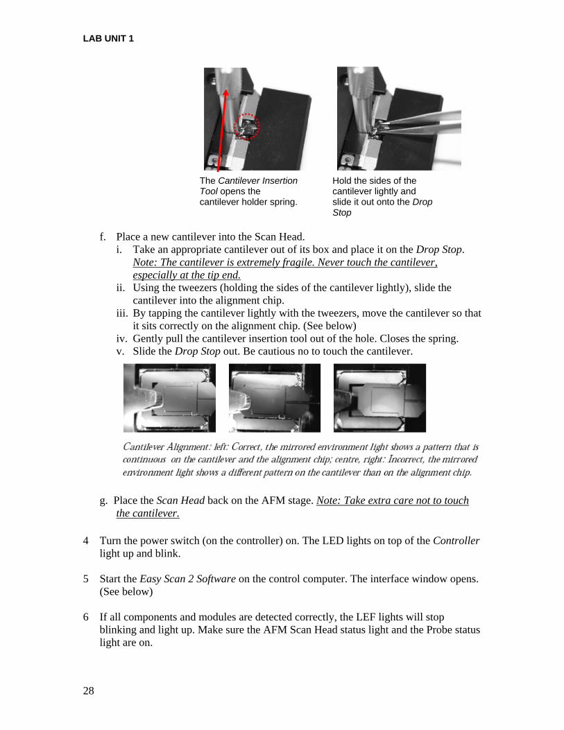
f. Place a new cantilever into the Scan Head.
i. Take an appropriate cantilever out of its box and place it on the Drop Stop. Note: The cantilever is extremely fragile. Never touch the cantilever, especially at the tip end.
ii. Using the tweezers (holding the sides of the cantilever lightly), slide the cantilever into the alignment chip.
iii. By tapping the cantilever lightly with the tweezers, move the cantilever so that it sits correctly on the alignment chip. (See below)
iv. Gently pull the cantilever insertion tool out of the hole. Closes the spring. v. Slide the Drop Stop out. Be cautious no to touch the cantilever.
g. Place the Scan Head back on the AFM stage. Note: Take extra care not to touch the cantilever.
4 Turn the power switch (on the controller) on. The LED lights on top of the Controller
light up and blink.
5 Start the Easy Scan 2 Software on the control computer. The interface window opens. (See below)
6 If all components and modules are detected correctly, the LEF lights will stop
blinking and light up. Make sure the AFM Scan Head status light and the Probe status light are on.
The Cantilever Insertion Tool opens the cantilever holder spring.
Hold the sides of the cantilever lightly and slide it out onto the Drop Stop
Scanning Force Microscopy & Dip-Pen Nanolithography
2007LaboratoryProgram/rev 29
Note: If the Probe Status light blinks red, it does not detect the cantilever in place. In that case, turn off the power switch, and readjust the cantilever following the step in 3.
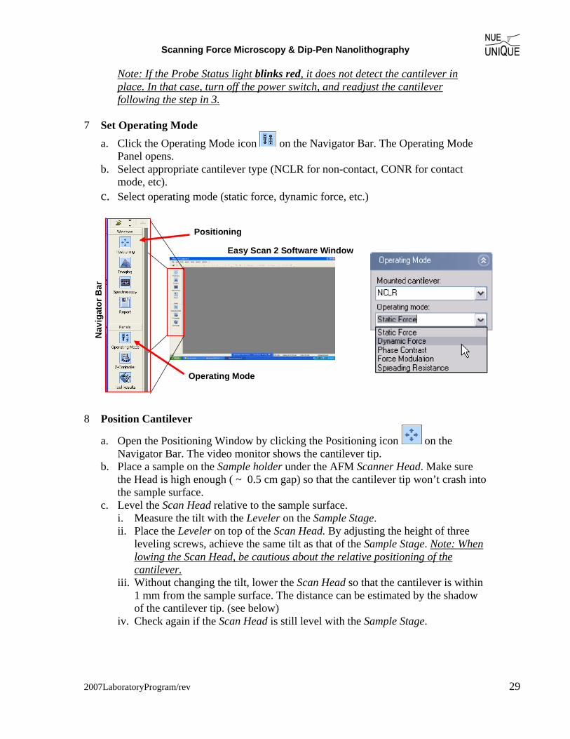
7 Set Operating Mode a. Click the Operating Mode icon on the Navigator Bar. The Operating Mode
Panel opens. b. Select appropriate cantilever type (NCLR for non-contact, CONR for contact
mode, etc). c. Select operating mode (static force, dynamic force, etc.)
Nav
igat
or B
ar
Positioning
Operating Mode
Easy Scan 2 Software Window
8 Position Cantilever
a. Open the Positioning Window by clicking the Positioning icon on the Navigator Bar. The video monitor shows the cantilever tip.
b. Place a sample on the Sample holder under the AFM Scanner Head. Make sure the Head is high enough ( ~ 0.5 cm gap) so that the cantilever tip won’t crash into the sample surface.
c. Level the Scan Head relative to the sample surface. i. Measure the tilt with the Leveler on the Sample Stage. ii. Place the Leveler on top of the Scan Head. By adjusting the height of three
leveling screws, achieve the same tilt as that of the Sample Stage. Note: When lowing the Scan Head, be cautious about the relative positioning of the cantilever.
iii. Without changing the tilt, lower the Scan Head so that the cantilever is within 1 mm from the sample surface. The distance can be estimated by the shadow of the cantilever tip. (see below)
iv. Check again if the Scan Head is still level with the Sample Stage.

LAB UNIT 1
30
Shadow
Too Close~ 1mm gap
9 Automatic Approach of Cantilever
a. Once the cantilever is approximately 1mm from shadow, automatic approach is used to bring the cantilever into contact. i. Open the Z-Controller Panel by clicking the icon in the Navigator bar. ii. Set the set point to be 5 nA(contact)/50%(non-contact). Use the default values
for the P-Gain, I-Gain, and D-Gain. iii. Click the Approach icon in Approach panel on the left side of the Positioning
window. iv. The software lowers the SFM tip till it comes in contact with the sample
surface. b. Once the approach is complete a message ‘Approach done’ appears and the
imaging panel automatically appears in the active window. c. Look at the Probe Status Light on the Controller. If it is NOT green, it is not
operating correctly. Immediately come out of contact by clicking Withdraw in the Approach Panel. Consult to a lab assistant.
d. The set point can be adjusted while the tip is in contact. In contact mode, increase of the value increases the normal force. In non-contact mode, increase of the value (%) decreases degree of tip-sample interaction.
10 Adjust the measurement plane For higher quality imaging and data collection, the sample surface is adjusted to be in parallel to the XY-plane of the SFM Scanner Head. a. Look at the slope of the sample surface on the Topography line graph, located
below the Topography image. b. If the slope of the topography in the imaging window is negative, the X-slope will
need to be increased. Start by increasing the slope by 0.1°. c. Increase the slope till the line is relatively parallel (no general slope) and the mean
fit scale (y-scale) is small.
Automatic Approach
Click off the Auto start imaging

Scanning Force Microscopy & Dip-Pen Nanolithography
2007LaboratoryProgram/rev 31
d. If the slope is positive decrease the slope by -0.1.
e. Once the slope is adjusted, the Y-direction slope is also adjusted. To do so, change the scan direction by typing in 90 ° in Rotation in Imaging Area window in the Imaging panel. Adjust the Y-slope in the same manner as X-slope.
11 Adjust the Controller Settings
Click on the Z-controller icon found on the Navigating bar (see below) and adjust the controller settings to keep tip-sample interactions constant. This is done by adjusting the feedback parameters, P, I, and D gain of the Z-controller.
i. Leave the P-gain at default value. Increase I-gain by 10% of the default value. Check in the topographic image if the contrast improves. If it shows a periodic stripe (shown in figure below), the I-gain is generating noise. Reduce it till the noise disappears.
ii. Increase the P-gain by 10 % of that default value. Stop when increasing the P-gain does not improve.
12 Ready for measurements. Proceed with instrument operational instructions specific to the lab unit.
Image Rotation
Noise
Z-Controller Icon
P and I Gain
X-Slope Y-Slope
Measured slope

LAB UNIT 1
32
3.7.2 Shutdown Procedure (1) Retract the cantilever as far as possible by auto-positioning. (2) Close the Easy Scan 2 soft ware window.
(3) Remove the cantilever (follow the instruction given in the Startup procedure step
(3)), and place the blank cantilever for the storage.
(4) Turn of the power switch on the Controller.
(5) Disconnect the Scan Head Cable and the Video Camera Cable.
(6) Place the Scan Head in the Scan Head Case.

Scanning Force Microscopy & Dip-Pen Nanolithography
2007LaboratoryProgram/rev 33
4. Scanning Probe Microscopy and Dip-Pen Nanolithography
Table of Contents:
4.1 Historic Perspectives ..................................................................................................................... 33 4.2 Scanning Force Microscopy (SFM) .............................................................................................. 34 4.2.1. Contact Mode ......................................................................................................................... 34 4.2.2. AC Mode Imaging ................................................................................................................. 35 4.2.3. Applied Force: Cantilever Deflection and Hooke’s Law ....................................................... 35 4.2.4. SFM Tips ............................................................................................................................... 36 4.3 Dip-Pen Nanolithography (DPN) .................................................................................................. 39
References ........................................................................................................................................... 40
4.1 Historic Perspectives
In 1982, Gerd Binnig and Heinrich Rohrer of IBM in Rüschlikon (Switzerland) invented scanning tunneling microscopy (STM). Although STM is not the focus of this lab, it is the ancestor of all the variations of scanning probe microscopy (SPM) that followed: although the mechanism of image contrast may vary, the idea of building up an image by scanning a very sharp probe across a surface has endured. As the name suggests, STM scans a sharp tip across a surface while recording the quantum mechanical tunneling current to generate the image. STM is capable of making extremely high resolution (atomic resolution) images of surfaces and has been extremely useful in many branches of science and engineering. For their invention, Binnig and Rohrer were awarded the Nobel Prize in Physics in 19861.
Although STM is able to obtain images with better than atomic resolution (some scientists even use it to image the electron orbitals around atoms in molecules), one limitation is that STM can only be used to image conductive surfaces. In an effort to overcome this restriction, Gerd Binnig, Christoph Gerber, and Calvin Quate at IBM and Stanford Univeristy developed scanning force microscopy (SFM), also known as atomic force microscopy (AFM), in 1986. SFM is a surface imaging technique that images both conductive and nonconductive surfaces by literally “feeling the surface”, i.e. measuring the force between a surface and an ultra sharp tip (typically 10 nm in radius). Fig. 4.1 shows a SFM image of a lipid bilayer.
Figure 4.1. SFM Image of Lipid Bilayer (scan size: 10 nm)
LAB UNIT 1
34
4.2 Scanning Force Microscopy (SFM)
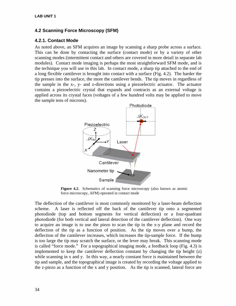
4.2.1. Contact Mode As noted above, an SFM acquires an image by scanning a sharp probe across a surface. This can be done by contacting the surface (contact mode) or by a variety of other scanning modes (intermittent contact and others are covered in more detail in separate lab modules). Contact mode imaging is perhaps the most straightforward SFM mode, and is the technique you will use in this lab. In contact mode, a sharp tip attached to the end of a long flexible cantilever is brought into contact with a surface (Fig. 4.2). The harder the tip presses into the surface, the more the cantilever bends. The tip moves in regardless of the sample in the x-, y- and z-directions using a piezoelectric actuator. The actuator contains a piezoelectric crystal that expands and contracts as an external voltage is applied across its crystal faces (voltages of a few hundred volts may be applied to move the sample tens of microns).
Figure 4.2. Schematics of scanning force microscopy (also known as atomic force microscopy, AFM) operated in contact mode
The deflection of the cantilever is most commonly monitored by a laser-beam deflection scheme. A laser is reflected off the back of the cantilever tip onto a segmented photodiode (top and bottom segments for vertical deflection) or a four-quadrant photodiode (for both vertical and lateral detection of the cantilever deflection). One way to acquire an image is to use the piezo to scan the tip in the x-y plane and record the deflection of the tip as a function of position. As the tip moves over a bump, the deflection of the cantilever increases, which increases the tip-sample force. If the bump is too large the tip may scratch the surface, or the lever may break. This scanning mode is called “force mode.” For a topographical imaging mode, a feedback loop (Fig. 4.3) is implemented to keep the cantilever deflection constant by changing the tip height (z) while scanning in x and y. In this way, a nearly constant force is maintained between the tip and sample, and the topographical image is created by recording the voltage applied to the z-piezo as a function of the x and y position. As the tip is scanned, lateral force are
Nanometer tip

Scanning Force Microscopy & Dip-Pen Nanolithography
2007LaboratoryProgram/rev 35
achieved on the lever on the lever due to friction causing the lever to torque. The motion can be with 4-quadrant segmented photodiodes.
Figure 4.3. Block Diagram of an SFM Feedback Loop. Kc is proportional gain; Ki is the integral gain; Kd is the derivative gain; e is the error.
4.2.2. AC Mode Imaging The SFM can also image a surface without continuously touching the surface. Such imaging modes⎯which can be classified as non-contact or intermittent-contact (Tapping Mode™ imaging by certain manufacturers)⎯are widely used, and are particularly suited to imaging soft surfaces such as polymers or biological samples. AC mode imaging gets its name from the fact that the tip is raised slightly above the surface and the cantilever is driven to vibrate near its resonant frequency (by yet another piezoelectric crystal). The amplitude, phase, and/or frequency of the cantilever are then monitored as the tip is scanned across the surface. The forces between the tip and the sample change the properties of the cantilever resonance, which can be used to generate a feedback signal and thus create an image. AC Mode imaging will be covered further in other lab modules so we will not discuss it further here.
4.2.3. Applied Force: Cantilever Deflection and Hooke’s Law The dimension, shape, and material of the cantilever tip can affect its resolution and sensitivity to different forces. In addition, tips with different coatings can be used in different applications of SPM. A conductive coating is required for electrostatic force microscopy (EFM), conductive atomic force microscopy (c-AFM), and etc. The most common commercial SFM tip is microfabricated from silicon or silicon nitride using conventional photolithography and semiconductor processing techniques, processes similar in many ways to those used to generate silicon computer chips. Hundreds to thousands of cantilever tips can be fabricated on a single wafer at once. The tip (with a tip radius of ~10 nm) is located at the free end of the cantilever that is typically 100 to 200 micron long (refer to Fig. 4.2). Shorter or thicker cantilevers have higher spring

LAB UNIT 1
36
constants and are more stiff. The cantilever acts like a spring and can be described by Hooke’s law:
zkF N−= Eq. (1)
where F is the force, kN is the normal spring constant, and z is the cantilever normal deflection. Typical spring constants available on commercially manufactured SFM cantilevers range from 0.01 N/m to 75 N/m. This enables forces as small as 10-9 N to be measured in liquids or an ultra-dry environment with the SFM. Analogous, lateral forces acting on the lever can be expressed as the product between a lateral spring constant kx and a lateral deflection x.
For a bar-shaped cantilever with length L, width W and thickness t, and an integrated tip of length r, the normal and lateral spring constants, kL and kx, are related to the material stiffnesses, as
3
3
4LEWtkN = and 2
3
3LrGWtk x = . Eq. (2)
where E and G respresent the normal Young’s modulus and the shear modulus, respectively.
The thickness of the cantilever, typically poorly defined by the manufacturers, can be determined from the first resonance frequency of the "free" cantilever using the following empirical equation:2
( ) E
L.
ft ρπ 128751041
2 22
1= . Eq. (3)
The Young's modulus and density of silicon cantilevers are around E = 1.69×10¹¹ N/m2
and ρ=2.33×10³ kg/m3.2
4.2.4. SFM Tips The lateral imaging resolution of SFM is intrinsically limited by the sharpness of the cantilever. Most commercial cantilevers have a tip with a 10 nm radius of curvature, although more exotic probes (such as those tipped with carbon nanotubes) are also available. Keep in mind that the resolution is also limited by the scanning parameters. For instance, if you take a 10 × 10 micron scan with a resolution of only 256 × 256 points, the size of each image pixel represents a lateral distance of 1 × 10⁻⁶ m / 256 = 39 nm.
As SFM images are generated by scanning a physical tip across the surface, this can lead to several image artifacts. One type of imaging artifact results from tip convolution. When the tip size is larger than the imaging feature size, the resulting image will be dominated by the shape of the tip. In this case, the observed features from the topography images will have very similar shapes despite the fact that the real features might be different (think of it as taking a picture of the tip with each of the surface features). Fig 4.4 shows two different sized tips scanned over a substrate with both small and large features. Also, damaged tips can often lead to distorted images. A tip with a piece of dirt stuck to it, or one that has been broken near the end can yield, for instance,

Scanning Force Microscopy & Dip-Pen Nanolithography
2007LaboratoryProgram/rev 37
doubled features as illustrated in Fig 4.5. One way to check for tip-induced artifacts is to rotate the scan angle by 90 degrees. If the shapes you are seeing do not rotate, the tip might be damaged!
Figure 4.4. Limitations of Tip Size. (Top) The large tip is much bigger than the small substrate feature. Each circle on the figure represents the position of the z-piezo recorded by the SFM as it moves across the sample. (Center) A small tip tracks both surface features better. (Bottom) The two line traces (large tip is dashed blue; small tip dotted green) from each tip are shown with the actual surface topography.
LAB UNIT 1
38
Figure 4.5 A minor case of doubled features caused by a damage tip. The image shows salt crystals embedded in polymer matrix.
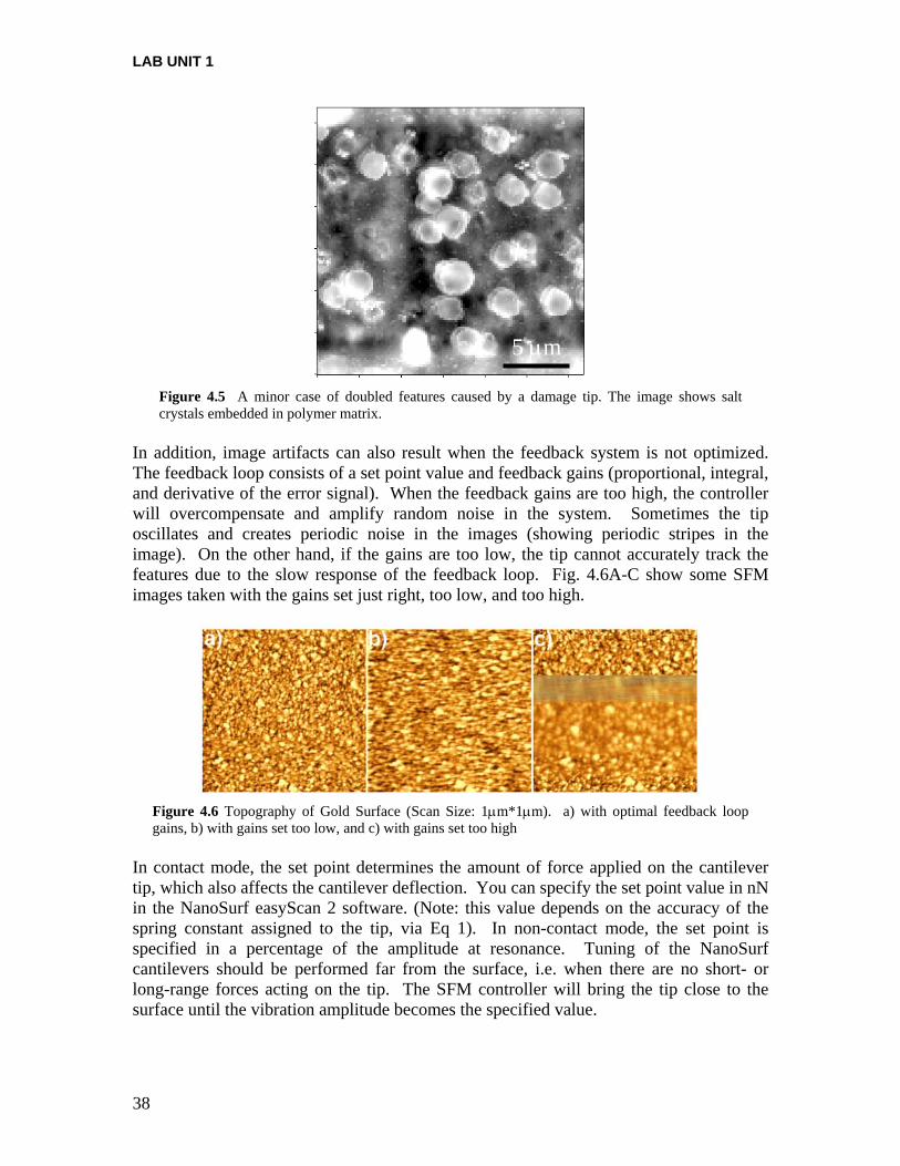
In addition, image artifacts can also result when the feedback system is not optimized. The feedback loop consists of a set point value and feedback gains (proportional, integral, and derivative of the error signal). When the feedback gains are too high, the controller will overcompensate and amplify random noise in the system. Sometimes the tip oscillates and creates periodic noise in the images (showing periodic stripes in the image). On the other hand, if the gains are too low, the tip cannot accurately track the features due to the slow response of the feedback loop. Fig. 4.6A-C show some SFM images taken with the gains set just right, too low, and too high.
Figure 4.6 Topography of Gold Surface (Scan Size: 1μm*1μm). a) with optimal feedback loop gains, b) with gains set too low, and c) with gains set too high
In contact mode, the set point determines the amount of force applied on the cantilever tip, which also affects the cantilever deflection. You can specify the set point value in nN in the NanoSurf easyScan 2 software. (Note: this value depends on the accuracy of the spring constant assigned to the tip, via Eq 1). In non-contact mode, the set point is specified in a percentage of the amplitude at resonance. Tuning of the NanoSurf cantilevers should be performed far from the surface, i.e. when there are no short- or long-range forces acting on the tip. The SFM controller will bring the tip close to the surface until the vibration amplitude becomes the specified value.
5 μm
Scanning Force Microscopy & Dip-Pen Nanolithography
2007LaboratoryProgram/rev 39
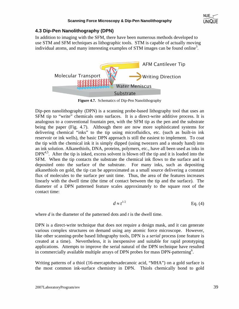
4.3 Dip-Pen Nanolithography (DPN) In addition to imaging with the SFM, there have been numerous methods developed to use STM and SFM techniques as lithographic tools. STM is capable of actually moving individual atoms, and many interesting examples of STM images can be found online3.
Figure 4.7. Schematics of Dip-Pen Nanolithography
Dip-pen nanolithography (DPN) is a scanning probe-based lithography tool that uses an SFM tip to “write” chemicals onto surfaces. It is a direct-write additive process. It is analogous to a conventional fountain pen, with the SFM tip as the pen and the substrate being the paper (Fig. 4.7). Although there are now more sophisticated systems for delivering chemical “inks” to the tip using microfluidics, etc. (such as built-in ink reservoir or ink wells), the basic DPN approach is still the easiest to implement. To coat the tip with the chemical ink it is simply dipped (using tweezers and a steady hand) into an ink solution. Alkanethiols, DNA, proteins, polymers, etc., have all been used as inks in DPN4,5. After the tip is inked, excess solvent is blown off the tip and it is loaded into the SFM. When the tip contacts the substrate the chemical ink flows to the surface and is deposited onto the surface of the substrate. For many inks, such as depositing alkanethiols on gold, the tip can be approximated as a small source delivering a constant flux of molecules to the surface per unit time. Thus, the area of the features increases linearly with the dwell time (the time of contact between the tip and the surface). The diameter of a DPN patterned feature scales approximately to the square root of the contact time: d ≈ t1/2 Eq. (4) where d is the diameter of the patterned dots and t is the dwell time. DPN is a direct-write technique that does not require a design mask, and it can generate various complex structures on demand using any atomic force microscope. However, like other scanning-probe based lithography tools, DPN is a serial process (one feature is created at a time). Nevertheless, it is inexpensive and suitable for rapid prototyping applications. Attempts to improve the serial natural of the DPN technique have resulted in commercially available multiple arrays of DPN probes for mass DPN-patterning6. Writing patterns of a thiol (16-mercaptohexadecanoic acid, “MHA”) on a gold surface is the most common ink-surface chemistry in DPN. Thiols chemically bond to gold
LAB UNIT 1
40
surfaces through their sulfur atom to form a gold-sulfur bond. The chemical reaction is generally accepted to be7:
R − SH + Au → R − S − Au +12
H 2
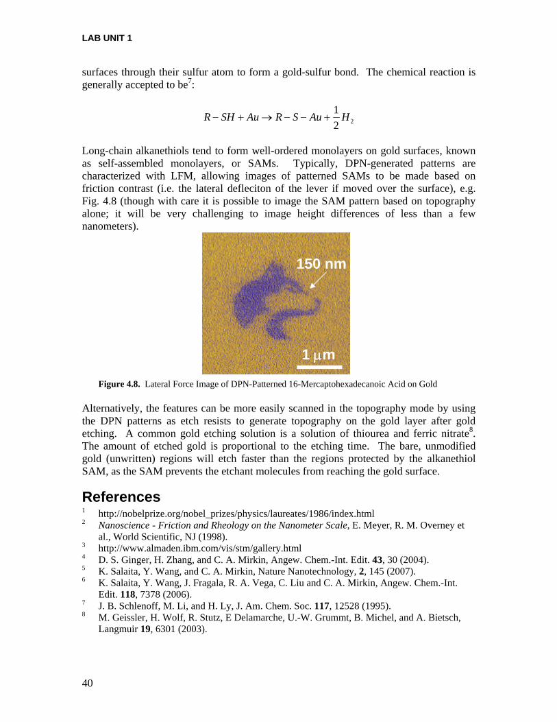
Long-chain alkanethiols tend to form well-ordered monolayers on gold surfaces, known as self-assembled monolayers, or SAMs. Typically, DPN-generated patterns are characterized with LFM, allowing images of patterned SAMs to be made based on friction contrast (i.e. the lateral defleciton of the lever if moved over the surface), e.g. Fig. 4.8 (though with care it is possible to image the SAM pattern based on topography alone; it will be very challenging to image height differences of less than a few nanometers).
Figure 4.8. Lateral Force Image of DPN-Patterned 16-Mercaptohexadecanoic Acid on Gold Alternatively, the features can be more easily scanned in the topography mode by using the DPN patterns as etch resists to generate topography on the gold layer after gold etching. A common gold etching solution is a solution of thiourea and ferric nitrate8. The amount of etched gold is proportional to the etching time. The bare, unmodified gold (unwritten) regions will etch faster than the regions protected by the alkanethiol SAM, as the SAM prevents the etchant molecules from reaching the gold surface.
References 1 http://nobelprize.org/nobel_prizes/physics/laureates/1986/index.html 2 Nanoscience - Friction and Rheology on the Nanometer Scale, E. Meyer, R. M. Overney et
al., World Scientific, NJ (1998). 3 http://www.almaden.ibm.com/vis/stm/gallery.html 4 D. S. Ginger, H. Zhang, and C. A. Mirkin, Angew. Chem.-Int. Edit. 43, 30 (2004). 5 K. Salaita, Y. Wang, and C. A. Mirkin, Nature Nanotechnology, 2, 145 (2007). 6 K. Salaita, Y. Wang, J. Fragala, R. A. Vega, C. Liu and C. A. Mirkin, Angew. Chem.-Int.
Edit. 118, 7378 (2006). 7 J. B. Schlenoff, M. Li, and H. Ly, J. Am. Chem. Soc. 117, 12528 (1995). 8 M. Geissler, H. Wolf, R. Stutz, E Delamarche, U.-W. Grummt, B. Michel, and A. Bietsch,
Langmuir 19, 6301 (2003).
1 μm
150 nm