wideband low noise amplifier design used for rf front end
TRANSCRIPT

IJRECE VOL. 7 ISSUE 2 APR.-JUNE 2019 ISSN: 2393-9028 (PRINT) | ISSN: 2348-2281 (ONLINE)
INTERNATIONAL JOURNAL OF RESEARCH IN ELECTRONICS AND COMPUTER ENGINEERING
A UNIT OF I2OR 2911 | P a g e
Wideband low noise amplifier design used for RF front
end application Tran Van Hoi1, Nguyen Van Thang1
1Faculty of Electrical and Electronic Engineering, Thuyloi University, Ha Noi, Viet Nam (E-mail: [email protected], [email protected])
Abstract— This paper discribes the design and fabrication
of a wideband low noise amplifier (LNA) at 4 - 5 GHz, which
suitable for RF front end application. The design of the LNA uses a single stage amplifier with center frequency 4.5GHz.
The LNA has been fabricated on a PCB board with FR4
subtrate using microstrip technology and pHEMT FET
transistor amplifier. The measured results show that the
maximum overall gain of 14.293 dB and gain flatness of ±0.5
dB over the 4-5 GHz frequency range; the noise figure is
about 1.515 dB; the reverse isolation of -34.5 dB. The LNA
using a 5 V supply voltage respectively and total current
consumptions of 20 mA. All the designed, simulated and
fabricated processes were done using Agilent’ ADS 2009
package and machine LPKF Protomat C40.
Keywords— Low noise amplifier, C band, noise figure,
satellite receiver, ADS.
I. INTRODUCTION
To amplify the very small received signals in satellite receiver systems, a low noise amplifier, which is placed right after the antenna, is required. The main interest of the LNA to the input of the analog processing chain is to amplify the signal without adding significant noise so as to allow a better analog and digital processing of information by following the modules of the LNA [1, 2]. Therefore, the goal of the designer is to design the LNA with gain as high as possible, the lowest noise figure and required wide band.
The general structure of LNA includes an active device characterized by its S-parameters and surrounded on both sides by impedance adaptation networks. The objective of this paper is to model a broadband low noise amplifier based on pHEMT FET transistors in the C-band with adaptation circuits of input and output using quarter wave transformers matching technique. First, we carry out a theoretical study of the circuit to stabilize and adapt it. Then we present some results of the design and simulation of the circuit (S-parameters, stability, gain, noise figure). Finally we discribes the experimental results.
II. MATCHING NETWORK
A. Power Gain
A single-stage amplifier with matching networks at the input and output terminals are shown in Fig.1. To transfer the maximum power from source to load, the source (ZS) and load
impedances (ZL) have to match to the input and output impedances of the transistor. In the figure, ZS and ZL are equal Z0 (50 Ω) [1].
Figure 1: The typical diagram of a single-stage amplifier.
The most useful gain definition for amplifier design is the
transducer power gain, which accounts on both source and load
mismatch. Thus from [4], we can define separate effective gain
factors for the input (Source) matching network, the transistor
itself and the output (Load) matching network as follows:
2
2
11
1
1
S
S
S
GS
(1)
2
0 21G S
(2)
2
2
22
1
1
L
L
L
GS
(3)
The overall transducer gain is GT = GS.G0.GL. The effective gains from GS and GL are due to the impedance matching of the transistor to the impedance Z0.
B. Stability of LNA
The stability of an amplifier, or its resistance to oscillate, is a very important consideration in a design and can be determined from the S parameters, the matching networks, and the terminations. The stability condition of an amplifier circuit is frequency dependent. In the circuit Fig.1, oscillations are possible when either the input or output port presents a
negative resistance. This occurs when |’in| >1 or |’out| >1. This is because and Ґout depends on the source and load matching networks. The stability of the amplifier depends on
S and L as presented by the matching networks. Thus, there are two types of stability.

IJRECE VOL. 7 ISSUE 2 APR.-JUNE 2019 ISSN: 2393-9028 (PRINT) | ISSN: 2348-2281 (ONLINE)
INTERNATIONAL JOURNAL OF RESEARCH IN ELECTRONICS AND COMPUTER ENGINEERING
A UNIT OF I2OR 2912 | P a g e
Unconditional stability: The network is unconditionally stable if |ГIN| < 1 and |ГOUT| < 1 for all passive source and load impedances.
Conditionally stability: The network is unconditionally stable if |ГIN| < 1 and |ГOUT| < 1 for a certain range of passive source and load impedances.
Consider that if the amplifier is unconditionally stable at a given frequency, the below equations must be satisfied:
21 1211
221
Lin
L
S SS
S
< 1 (4)
21 1222
111
sout
S SS
S s
< 1 (5)
Another parameter must take into account the stability factor K [3], defined as:
(6)
Along with the auxiliary condition that
(7)
III. DESIGN OF LNA
The design process adopted in this article is based on three essential steps. First, type of transistor to be used was determined; we opted for the pHEMT GaAs FET transistor spf-3043 of Stanford Microdevices. Then the choice of circuit topology is made. Afterwards, the matching circuit is established.
Design of the low noise amplifier competes with such factors as stability, gain, bandwidth and noise figure. For instance, a minimum noise performance at a maximum gain cannot be obtained. It is therefore, important to optimize characteristics to trade-offs between gain, stability, bandwidth and noise figure.
The noise figure of the amplifier at this frequency is calculated to be as follows [4]:
2
min 2 2
4( )1 (1 )
opt sN
o opt S
RF F
Z
(8)
From the S parameters and noise parameters at 4.5 GHz is provided by NEC we can find the parameters of noise figure as
follows: Minimum noise figure Fmin, opt, the noise resistance RN = 50*rn. In order to obtain the minimum noise figure, the
reflection coefficient S look into the source is matched to opt.
In addition, in is set to be the conjugate of S, the reflection coefficient looking into the load is shown below:
* 22
111
SL
S
S
S
(9)
In order to transfer the maximum power from the input
matching networks to the transistor will occur when S = *in =
S*11 and the maximum power transfer from the transistor to the
output matching network will occur when L = *out = S*
22.
The value of S and L is after that used for the design of the input and output matching networks using smith chart. The matching networks can be designed by some methods such as using lumped components, stubs, quarter-wave transformer or using general transmission line. However, to design a wide band LNA, the quarter-wave transformer matching and general transformer is the best choice.
For a transmission line of the characteristic impedance Z0 and length l, the input impedance Zin can be written as following in [1].
(10)
such as:
(11)
Then, if an intermediate section of transmission line with a
characteristic impedance Z/4 and a quarter wavelength long is connected between the main line and the load, as illustrated in fig. 2.
Figure 2. Quarter wave transformers
The impedance presented to the main line would be equal to [2]:
(12)
The adaptation condition is verified if:
(13)
This implies that: Zin = Z0.
The completed LNA with two-stage was shown in Fig.3. The power supply for spf-3043 is 5V/20 mA and the voltage of biasing point is obtained at -0.7V.
IJRECE VOL. 7 ISSUE 2 APR.-JUNE 2019 ISSN: 2393-9028 (PRINT) | ISSN: 2348-2281 (ONLINE)
INTERNATIONAL JOURNAL OF RESEARCH IN ELECTRONICS AND COMPUTER ENGINEERING
A UNIT OF I2OR 2913 | P a g e
Figure 3: Schematic of the LNA
IV. SIMULATED RESULTS
The initial simulations to test the LNA performance were done with the s-parameter file of the transistor. The results were shown in the bellow Figs.
Fig 4: The S21 and S12 of the LNA.
The Fig.4 displays the parameters which have been achieved: overall gain is greater than 14.93 dB from 4 GHz to 5 GHz and the maximum gain obtains 18.870.54 dB at 4.0GHz. the value of reverse isolation (S12) is very good in working band, and less than -20.6 dB.
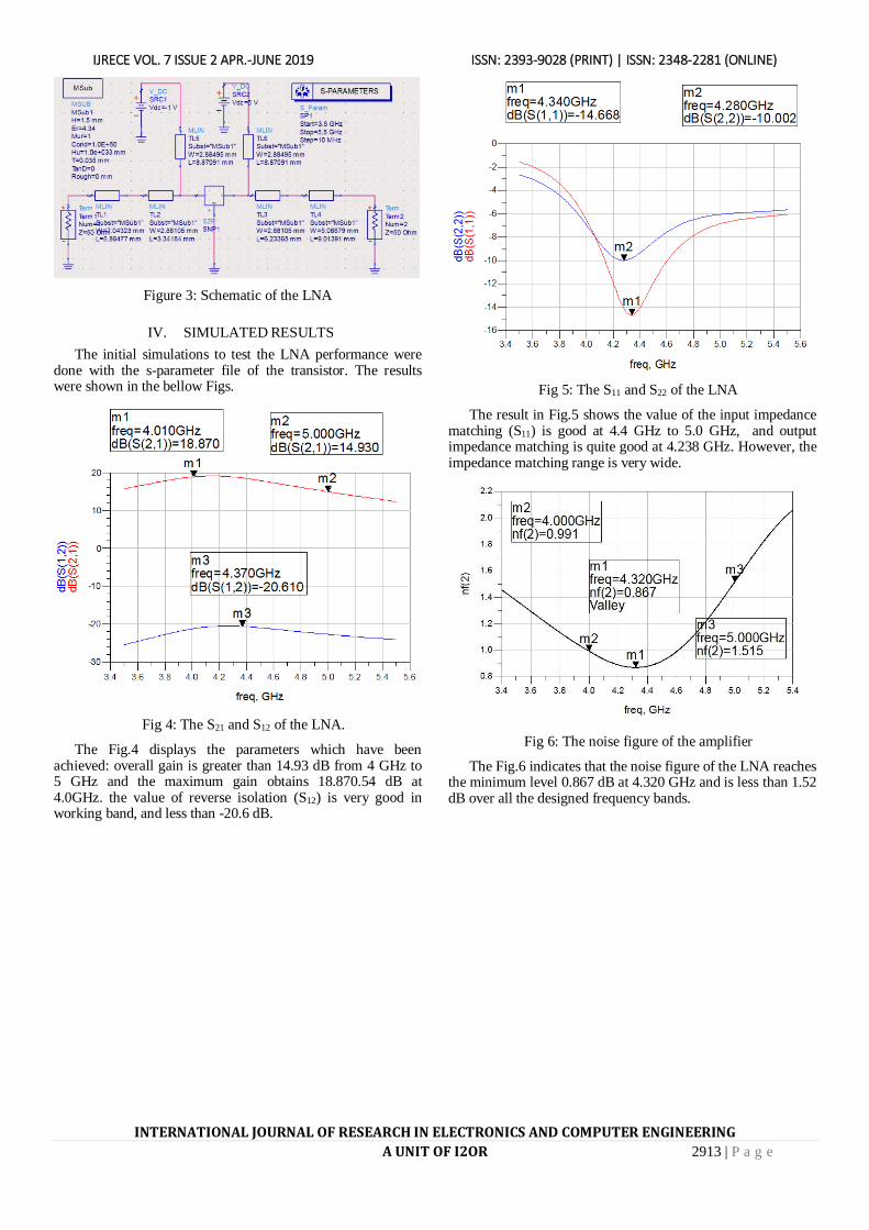
Fig 5: The S11 and S22 of the LNA
The result in Fig.5 shows the value of the input impedance matching (S11) is good at 4.4 GHz to 5.0 GHz, and output impedance matching is quite good at 4.238 GHz. However, the impedance matching range is very wide.
Fig 6: The noise figure of the amplifier
The Fig.6 indicates that the noise figure of the LNA reaches the minimum level 0.867 dB at 4.320 GHz and is less than 1.52 dB over all the designed frequency bands.
IJRECE VOL. 7 ISSUE 2 APR.-JUNE 2019 ISSN: 2393-9028 (PRINT) | ISSN: 2348-2281 (ONLINE)
INTERNATIONAL JOURNAL OF RESEARCH IN ELECTRONICS AND COMPUTER ENGINEERING
A UNIT OF I2OR 2914 | P a g e
Fig. 7: The stability factor of LNA
The gragh in Fig.7 exhibits the K value is greater than 1, it mean that the LNA to be stable at 4 to 5 GHz.
V. EXPERIMENTAL RESULTS
The LNA circuit was fabricated in Laboratory with the aid of the ADS package and machine LPKF Promomat C40. The circuit was supplied Vds and Vgs through the DC pins at the top of the board. The drain current was measured to be about 20 mA. The result was shown in Fig. 8.
Fig 8: The fabricated LNA
The testing results visually are measured on the vector network analyzer 37369D - Anritsu technology up to 40 GHz and the Signal Analyzer FSQ.
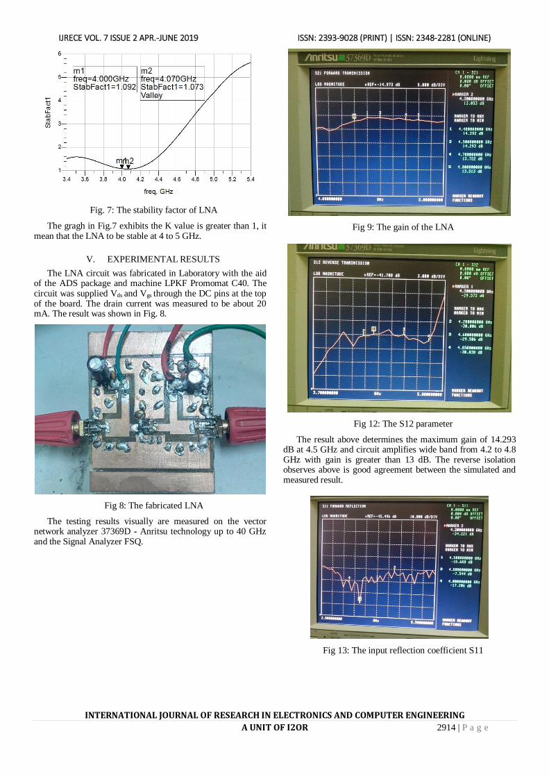
Fig 9: The gain of the LNA
Fig 12: The S12 parameter
The result above determines the maximum gain of 14.293 dB at 4.5 GHz and circuit amplifies wide band from 4.2 to 4.8 GHz with gain is greater than 13 dB. The reverse isolation observes above is good agreement between the simulated and measured result.
Fig 13: The input reflection coefficient S11

IJRECE VOL. 7 ISSUE 2 APR.-JUNE 2019 ISSN: 2393-9028 (PRINT) | ISSN: 2348-2281 (ONLINE)
INTERNATIONAL JOURNAL OF RESEARCH IN ELECTRONICS AND COMPUTER ENGINEERING
A UNIT OF I2OR 2915 | P a g e
Fig 14: The output reflection coefficient
Looking into the results, both simulated and measured results show similar response. Whereas the measured S11 resonates at 4.3 GHz, compared to 4.23 GHz of the simulation and the measured S22 resonates at 4.5 GHz, compared to 4.55 GHz of the simulation. However, the measured results have been observed to be greater than simulation.
VI. CONCLUSION
A single-stage LNA with spf-3043 is designed and demonstrated with simulations in ADS package as well as tuning for the optimum gain, noise figure and bandwidth. The design was fabricated and the board was measured and analyzed together with the simulated results. The benefits of this LNA design are the stability of its performances throughout the wideband frequency range, high gain, low noise and smaller PCB fabrication. Overall, this LNA could be used for the RF front end application working at 4 – 5GHz.
REFERENCES
[1] David M. Pozar, Microwave Engineering, 3nd Edition, John Wiley & Sons, Inc- New York, United State of America, chap 11, 2005.
[2] G. Gonzalez, Microwave transistor amplifiers – analysis and design, second dition, Prentice Hall, Inc, 1997.
[3] A. Abhimanyu, P. Aswathy, D. Athira, G. Gayathry, Design Of Low Noise Amplifier At 4 Ghz, International Conference on Information and Electronics Engineering, 2011, pp 209 – 212.
[4] A. F. Osman and N. Mohd. Noh, Wideband LNA Design for SDR Radio using Balanced Amplifier Topology, 4th Asia Symposium on Quality Electronic Design, 2012, pp.86-90.
[5] Tran Van Hoi, Bach Gia Duong, “Study and design of wideband low noise amplifier operating at C band, Journal of Mathematics
– Physics, Vietnam National University, vol. 29, no. 2, pp.16-24, 2013.
[6] Othman A.R, Ibrahim A.B, Husain M.N, Ahmad M.T, Senon M., “High Gain Low Noise Cascode LNA Using T-Matching Network for Wireless Applications”, IEEE Asia-Pacific Conference on Applied Electromagnetics (APACE 2012), 2012, pp 383 - 387.
[7] Zhihong Dai; Yongzhong Hu; Kunzhi Xu, “Two-stage Low Noise Amplifier for BD-II Receiver Application”, 5th Global Symposium on Millimeter Waves (GSMM 2012), 2012, pp. 303-306.
[8] Z. Abolfazl, A. B. Masih, A. Jafar, D. Masoud, “A 3-5 GHz Ultra Wideband Common-Gate Low Noise Amplifier”, 2012 IEEE International Conference on Circuits and Systems (ICCAS).
[9] Tran Van Hoi, Hoang Duc Long, Bach Gia Duong, “Low noise block downconverter design for satellite receiver system Vinasat 1 operating at C-band”, International Conference on Intergrated Circuits, Design, and Verification, pp.110-115, 2013.
Dr. Tran Van Hoi received the B.S degree in telecommunication techniques from University of Transport and communications (UTC) in 2001. He
obtained M.S degree in electronic wireless and communication from Le Quy Don Technical University in 2004. He received Ph.D degree in Electronics and Communication Technology in University of Engineering and Technology, Viet Nam National University in 2018. Now He has been working in Thuy Loi University. His
research interests involves in RF design, RF chip design, Satellite Communication. Email: [email protected]
Dr. Nguyen Van Thang was born in 1979. He received his B.Sc., degree in Electronics and Telecommunication at the Hanoi University of Transport and
Communications, Hanoi, Vietnam, in 2002 and his M.Sc. degree in Information Engineering from Le Quy Don University, Hanoi, Vietnam, in 2007. He received his PhD. degree in Electronics and Telecommunication at VNU University of Engineering and Technology. Now, he is lecturer at ThuyLoi University. Until now, he is author and coauthor of some papers on
MEMS based sensors and their application.