why this dsp is so sweet! - university of...
TRANSCRIPT


WHY THIS DSP IS SO SWEET!
� Space-saving multiplexer design
� High performance adder topology
� Area-conscious adder-subtractor combination
� Advanced multiplier implementation

MULTIPLEXER � Space-saving! But how?
� By utilizing pass-gate transistor logic, Team NAND was able to cut the amount of transistors down from a standard multiplexer design (8 4-input ANDs and an 8-input OR)
from 104 transistors to only 24! That’s approximately 1/4th the size! � But aren’t there swing issues associated with such an approach?
� Yes! But Team NAND solved this issue by buffering the output (which was
included in the 24 transistor count), providing a fully functional 8x1 MUX! � Are there any other advantages?
� Of course! The lower fanout associated with this topology means less power consumption and less delay. Our tests showed a .02ns delay vs .1ns delay…
that’s 5 times as fast!

STANDARD MUX SCHEMATIC
Input Double Inverter
Load Inverter
Select line inverter
4Input AND Gates
8 Input OR Gate
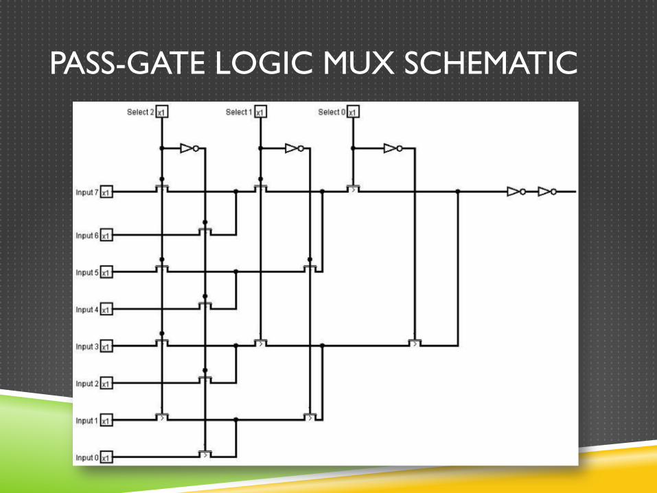
PASS-GATE LOGIC MUX SCHEMATIC

ADDER � High performance! But how?
� Team NAND decided to use the go-to industry-standard adder topology for speed,
speed, speed – the Kogge-Stone parallel prefix adder! � What makes it so fast?
� In a parallel prefix adder (PPA), a prefix operation is constructed that permits the computation of intermediate carries. This allows PPAs to obtain an
advantageous latency of O(log2N) instead of O(N) (like in a Ripple Carry adder), where N is the word length.
� What does that even mean!?
� This means our adder provides blazing fast computations! We put our
Kogge-Stone to the test and found it to be 12 times faster than a standard Ripple Carry when exercising the critical path (.03ns delay vs .36 delay), which would only get faster for increased bit-width!

ADDER � Wouldn’t such an advantageous adder consume equally as much current
and power?
� You’d think so, but nope! Our tests showed only a .05mA increase in
current (1.14mA vs 1.09mA) and only a ~3.5mW increase in power consumption (6.27mW vs 2.55mW)!
� How exactly does it work? � A generate and propagate signal are created in the first stage that are then used to
compute the intermediate carries in parallel. The final sum is an XOR of the carry and propagate signals
� So why specifically a Kogge-Stone? � The attributes associated with a Kogge-Stone are low logic depth, high node count,
and minimal fanout. While a high node count implies a larger area, the low logic depth and minimal fanout allow for faster performance!

ADDER TREE DIAGRAM
ß An example of an 8-bit Kogge-Stone parallel prefix adder
^ The critical path through our 16-bit Kogge-Stone
16-bit K-S Diagram: http://www.aoki.ecei.tohoku.ac.jp/arith/mg/image/ksa.gif

ADDER SCHEMATIC

ADDER-SUBTRACTOR � Area-conscious! How so?
� By realizing that A – B in two’s complement is merely A + B’ + 1, we were able to
utilize our high performance adder topology. This meant speedy subtractions and that instead of having two redundant copies of the adder in
the same DSP, we utilized a 16-bit 2x1 MUX and a 16-bit inverter to switch between the two functions.
� How exactly does that help? � While having a combined adder-subtractor slightly increases delay (.16ns in our
tests), we were able to save 57.6% in area by combining the two (435μm vs 755μm)!
ADDER-SUBTRACTOR � Are there any other advantages?
� Of course! Utilizing a combined adder and subtractor means a multitude of savings in power consumption, as there is no redundant adder topology operating simultaneously!
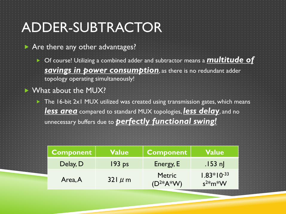
� What about the MUX? � The 16-bit 2x1 MUX utilized was created using transmission gates, which means
less area compared to standard MUX topologies, less delay, and no
unnecessary buffers due to perfectly functional swing!
Component Value Component Value
Delay, D 193 ps Energy, E .153 nJ
Area, A 321μm Metric
(D2*A*W) 1.83*10-33
s2*m*W

MULTIPLIER � Advanced?
� The common go-to multiplier topology is an array multiplier that ANDs the inputs to create partial products, then uses adders to compute the final product. Unfortunately,
due to this multiplying scheme, its functionality is hampered by an O(log2n) computation time. Fortunately, however, a Wallace tree multiplier serves as a much more efficient multiplication scheme.
� What makes it so fast?
� By reducing the number of partial products by two layers of full and half adders, and using a high performance adder to compute the final product, the Wallace tree
multiplier achieves an advantageous computation time of O(log2N). However,
Team NAND was not satisfied with this improvement and decided to go for
an even more advanced topology called the Dadda multiplier.

MULTIPLIER
� Why is the Dadda multiplier better? � The Dadda multiplier is similar to the Wallace
multiplier, but is slightly faster for all operand sizes and requires fewer gates. What this translates to for PICo is a
DSP with a high performance multiplier, which keeps area and power in consideration by requiring fewer gates.
Component Value Component Value
Delay, D 603 ps Energy, E .478 nJ
Area, A 259μm Metric (D2*A*W)
4.50*10-32 s2*m*W
Wallace Diagram: http://en.wikipedia.org/wiki/File:Wallace_tree_8x8.svg Dadda Diagram: http://en.wikipedia.org/wiki/File:Dadda_tree_8x8.svg

DSP RESULTS
Component Value Component Value
Delay, D 196 ps Energy, E .963 nJ
Area, A 435μm Metric (D2*A*W) 1.61*10-32 s2*m*W

DSP FUNCTIONALITY SIMULATION

DSP ENERGY SIMULATION

CONCLUSION � While the DSP had certain requirements, Team NAND took it upon
themselves to implement high performance topologies, space-saving circuits, and a highly advanced multiplier technology
� The pass-gate logic multiplexer utilized, buffered to compensate for swing, serves effective functionality while vastly reducing area, delay, and power consumption when compared to our competitors’ common multiplexer design
� The advanced Kogge-Stone parallel prefix adder provides O(log2N) latency, producing a critical path delay twelve times less than the standard Ripple Carry topology used by our competitors

CONCLUSION
� The combined adder-subtractor allows for greatly reduced area (a savings of 57.6% over having a separate adder and subtractor), while reducing overall power consumption, yet still providing exceedingly fast performance.
� Our Dadda tree multiplier not only surpasses the performance of common array multipliers; but also, is even faster and utilizes less gates than our competitors’ Wallace tree multipliers.
� Thusly, we conclude, that by the implementation of our innovations, Team NAND is the best choice for PICo
Thank you, Kyle, Andrew, Jacob, Izak, and Kenny