w/d-bands single-chip systems in a 0.13μm...
TRANSCRIPT

W/D-Bands Single-Chip Systems in a 0.13μm SiGe
BiCMOS Technology – Dicke Radiometer, and
Frequency Extension Module for VNAs
by
EŞREF TÜRKMEN
Submitted to the Graduate School of Engineering and Natural Sciences
in partial fulfillment of
the requirements for the degree of
Master of Science
Sabanci University,
Summer, 2018

ii

iii
© Esref Turkmen 2018
All Rights Reserved

iv
Acknowledgments
First and foremost, I would like to express my deepest gratitude to my research supervisor
Prof. Yasar Gurbuz, for his invaluable advice, support in many aspects of this work, and
guidance over the past three years.
Besides my advisor, I would also like to thank my committee members, Assoc. Prof.
Meric Ozcan, professor Assoc. Prof. Burak Kelleci for serving as my thesis committee
members and for their insightful comments and valuable feedback.
I am very thankful to my friends and colleagues in the Sabanci University
Microelectronics Research Group (SUMER), Dr. Melik Yazici, Dr. Omer Ceylan, Ilker
Kalyoncu, Abdurrahman Burak, Emre Can Durmaz, Elif Gül Ozkan Arsoy, Alper Guner,
Can Caliskan, Hamza Kandis, Tahsin Alper Ozkan, Isık Berke Gungor, Cerin Ninan
Kunnatharayil, Shahbaz Abbasi, and Atia Shafique for creating such a friendly working
environment, including the past members Barbaros Cetindogan, Berktug Ustundag,
Mesut Inac, and Murat Davulcu. I also thank the laboratory specialist Ali Kasal for his
help and support. In addition, I thank to Ali, Alican, Bahadir, Deniz, Kaan, Oguz, Volkan
and many others for their friendship.
A special thanks to my family. I would like to express my gratitude to my mother Arife,
my father Orhan, and my brother Nazim Eren for their unconditional love, eternal support,
and assurances that they have shown throughout my life. Finally, I would like to express
appreciation to my beloved girlfriend Didem Dilara for her support and patience during
my thesis research and the thesis writing period.

v
W/D-Bands Single-Chip Systems in a 0.13μm SiGe BiCMOS Technology
– Dicke Radiometer, and Frequency Extension Module for VNAs
Esref Turkmen
EE, Master’s Thesis, 2018
Thesis Supervisor: Prof. Dr. Yasar Gurbuz
Keywords: millimeter-wave integrated circuits, passive imaging systems, frequency
extension modules, SiGe BiCMOS.
Abstract
Recent advances in silicon-based process technologies have enabled to build low-cost and
fully-integrated single-chip millimeter-wave systems with a competitive, sometimes even
better, performance with respect to III-V counterparts. As a result of these developments
and the increasing demand for the applications in the millimeter-wave frequency range,
there is a growing research interest in the field of the design and implementation of the
millimeter-wave systems in the recent years. In this thesis, we present two single-chip D-
band front-end receivers for passive imaging systems and a single-chip W-band
frequency extension module for VNAs, which are implemented in IHP’s 0.13μm SiGe
BiCMOS technology, SG13G2, featuring HBTs with 𝑓𝑡/𝑓𝑚𝑎𝑥 of 300GHz/500GHz.
First, the designs, implementations, and measurement results of the sub-blocks of the
radiometers, which are SPDT switch, low-noise amplifier (LNA), and power detector, are
presented. Then, the implementation and experimental test results of the total power and
Dicke radiometers are demonstrated. The total power radiometer has a noise equivalent
temperature difference (NETD) of 0.11K, assuming an external calibration technique. In
addition, the dependence of the NETD of the total power radiometer upon the gain-
fluctuation is demonstrated. The NETD of the total power radiometer is 1.3K assuming a
gain-fluctuation of %0.1. The front-end receiver of the total power radiometer occupies
an area of 1.3 mm2. The Dicke radiometer achieves an NETD of 0.13K, for a Dicke
switching of 10 kHz, and its total chip area is about 1.7 mm2. The quiescent power
consumptions of the total power and Dicke radiometers are 28.5 mW and 33.8 mW,
respectively. The implemented radiometers show the lowest NETD in the literature and
the Dicke switching concept is employed for the first time beyond 100 GHz.
Second, we present the design methodologies, implemantation methods, and results of
the sub-blocks of the frequency extension module, such as down-conversion mixer,
frequency quadrupler, buffer amplifier, Wilkinson power divider, and dual-directional
coupler. Later, the implemantation, characterization and experimental test results of the
single-chip frequency extension module are demonstrated. The frequency extension
module has a dynamic range of about 110 dB, for an IF resolution bandwidth of 10 Hz,
with an output power which varies between -4.25 dBm and -0.3 dBm over the W-band.
It has an input referred 1-dB compression point of about 1.9 dBm. The directivity of the
frequency extension module is better than 10 dB along the entire W-band, and its
maximum value is approximately 23 dB at around 75.5 GHz. Finally, the measured s-
parameters of a W-band horn-antenna, which are performed by either the designed
frequency extension module and a commercial one, are compared. This study is the first
demonstration of a single-chip frequency extension module in a silicon-based
semiconductor technology.

vi
0.13μm SiGe BiCMOS W/D-Band Tek-Çip Sistemler – Dicke
Radyometresi, ve VNA’lar için Frekans Genişletici Modül
Eşref Türkmen
EE, Yüksek Lisans Tezi, 2018
Tez Danışmanı: Prof. Dr. Yaşar Gürbüz
Anahtar Kelimeler: milimetre-dalga frekansı, pasif görüntüleme sistemleri, frekans
genişletici modüller, SiGe BiCMOS.
Özet
Silikon bazlı proses teknolojilerindeki son gelişmeler, düşük maliyetli ve tamamen
entegre tek çipli milimetre-dalga sistemlerinin, III-V muadillerine göre rekabetçi, bazen
daha da iyi bir performansa sahip olmasını sağlamıştır. Bu gelişmeler ve milimetrik dalga
frekansı alanındaki uygulamalara olan artan talebin bir sonucu olarak, son yıllarda
milimetre-dalga sistemlerinin tasarımı ve uygulanması alanında giderek artan bir
araştırma ilgisi bulunmaktadır. Bu tez çalışmasında, IHP'nin 0.13μm SiGe BiCMOS
teknolojisinde gerçeklenen, tekli çipli D-bant ön uç alıcıları (toplam güç ve Dicke
radyometre) ve VNA'lar için tek çipli W-bant frekans uzatma modülü sunulmaktadır.
İlk olarak, SPDT anahtarı, düşük gürültü kuvvetlendirici (LNA) ve güç dedektörü olan
radyometrelerin alt bloklarının tasarımları, uygulamaları ve ölçüm sonuçları
sunulmaktadır. Daha sonra, toplam güç ve Dicke radyometrelerinin gerçeklenmesi ve
deneysel test sonuçları gösterilmiştir. Toplam güç radyometresi, harici bir mekanik
anahtarlama olduğu varsayılarak 0.07K'lık bir gürültü eşdeğer sıcaklık farkına (NETD)
sahiptir. Ek olarak, toplam güç radyometrisinin NETD'nin kazanım-dalgalanması
üzerindeki bağımlılığı gösterilmektedir. Toplam güç radyometresinin NETD'si,% 0.1'lik
bir kazanç dalgalanması varsayılarak 1.3K olarak bulunmuştur. Toplam güç
radyometresinin ön uç alıcısı 1.3 mm2'lik bir alanı kaplar. Dicke radyometresi, 10 kHz'lik
bir Dicke anahtarlaması için 0.13K'lık bir NETD elde eder ve toplam yonga alanı yaklaşık
1.7 mm2'dir. Toplam gücün ve Dicke radyometrelerinin sukunet halinde güç tüketimi
sırasıyla 28.5 mW ve 33.8 mW'dir. Gerçeklenen radyometreler literatürdeki en düşük
NETD performansını gösterir ve Dicke anahtarlama kavramı 100 GHz'nin ötesinde ilk
kez kullanılmıştır.
İkincisi, aşağı-dönüşüm karıştırıcısı, frekans dörtleyici, tampon kuvvetlendirici,
Wilkinson güç bölücü ve çift yönlü kuplör gibi frekans genişletme modülünün alt-
bloklarının tasarım metodolojilerini, gerçeklenme yöntemlerini ve elde edilen sonuçları
sunulmaktadır. Daha sonra, tek çipli frekans uzatma modülünün implemantasyon,
karakterizasyon ve deneysel test sonuçları gösterilmiştir. Frekans uzatma modülü, 10
Hz'lik bir IF çözünürlük bant genişliği için yaklaşık 110 dB'lik bir dinamik aralığa sahiptir
ve W-bandı üzerinde -4.25 dBm ve -0.3 dBm arasında değişen bir çıkış gücü vardır. Girişe
tanımlı 1 dB sıkıştırma noktası yaklaşık 1.9 dBm’dir. Frekans genişletme modülünün
yönelimi tüm W-bandı boyunca 10 dB'den daha iyidir ve maksimum değeri yaklaşık 75.5
GHz'de yaklaşık 23 dB'dir. Son olarak, tasarlanan frekans uzatma modülü ve ticari bir
tanesi tarafından gerçekleştirilen bir W-band horn-anteninin ölçülen s-parametreleri
karşılaştırılır ve tek-çipli frekans uzatma modülünün çalışması bu şekilde doğrulanır. Bu
çalışma, bir silikon tabanlı yarı iletken teknolojisinde uygulanan tek-çip frekans uzatma
modülünün ilk gösterimidir.

vii
Contents
Acknowledgments ........................................................................................................... iv
Abstract ............................................................................................................................. v
Özet .................................................................................................................................. vi
Contents ......................................................................................................................... vii
List of Figures .................................................................................................................. ix
List of Tables .................................................................................................................. xv
List of Abbreviations ..................................................................................................... xvi
1. Introduction ............................................................................................................... 1
1.1. Millimeter-wave Monolithic Integrated Circuits ............................................... 1
1.2. Characterizations of Millimeter-wave Monolithic Integrated Circuits .............. 4
1.3. SiGe BiCMOS Technology................................................................................ 7
1.4. Motivation .......................................................................................................... 8
1.5. Organization ....................................................................................................... 9
2. D-Band Total Power and Dicke Radiometers ......................................................... 11
2.1. Fundamentals of Passive Imaging Systems ..................................................... 11
2.1.1 Detection Principles........................................................................................ 11
2.1.2 Radiometer Architectures and Theoretical Sensitivity Calculations .............. 15
2.2. Power Detector ................................................................................................. 23
2.2.1 Circuit Design and Implementation ................................................................ 23
2.2.2 Simulation and Measurement Results ............................................................ 34
2.2.3 Comparison..................................................................................................... 41
2.3. Low-Noise Amplifier ....................................................................................... 42
2.3.1 Circuit Design and Implementation ................................................................ 42
2.3.2 Simulation and Measurement Results ............................................................ 52
2.3.3 Comparison..................................................................................................... 56
2.4. SPDT Switch .................................................................................................... 57
2.4.1 Circuit Design and Implementation ................................................................ 57
2.4.2 Simulation and Measurement Results ............................................................ 60
2.4.3 Comparison..................................................................................................... 62
2.5. Total Power and Dicke Radiometers ................................................................ 64
2.5.1 Implementation ............................................................................................... 64
2.5.2 Measurement Results...................................................................................... 65

viii
2.5.3 Comparison..................................................................................................... 72
3. W-Band Frequency Extension Module for VNAs .................................................. 74
3.1. S-Parameter Measurements Using Frequency Extension Modules ................. 74
3.1.1 Network Analyzer .......................................................................................... 74
3.1.2 Frequency Extension Module ......................................................................... 81
3.1.3 Single-Chip Frequency Extender and System Simulations ............................ 85
3.2. Down-Conversion Mixer ................................................................................. 87
3.2.1 Circuit Design and Implementation ................................................................ 87
3.2.2 Simulation and Measurement Results ............................................................ 92
3.2.3 Comparison..................................................................................................... 98
3.3. Frequency Quadrupler ...................................................................................... 99
3.3.1 Circuit Design and Implementation ................................................................ 99
3.3.2 Simulation and Measurement Results .......................................................... 102
3.3.3 Comparison................................................................................................... 105
3.4. Buffer Amplifiers ........................................................................................... 105
3.4.1 Circuit Design and Implementation .............................................................. 105
3.4.2 Simulation Results ........................................................................................ 108
3.5. Dual-Directional Coupler ............................................................................... 110
3.5.1 Circuit Design and Implementation .............................................................. 110
3.5.2 Simulation Results ........................................................................................ 111
3.6. Wilkinson Power Divider ............................................................................... 113
3.6.1 Circuit Design and Implementation .............................................................. 113
3.6.2 Simulation Results ........................................................................................ 114
3.7. Frequency Extension Module ........................................................................ 115
3.7.1 Implementation ............................................................................................. 115
3.7.2 Characterization ............................................................................................ 116
3.7.3 Measurement Results.................................................................................... 122
4. Conclusion & Future Work ................................................................................... 125
4.1. Summary of Work .......................................................................................... 125
4.2. Future Work ................................................................................................... 126
APPENDIX ................................................................................................................... 128
REFERENCES ............................................................................................................. 130

ix
List of Figures
Figure 1 Amount of atmospheric attenuation for various relative humidity (RH) values
[12]. ................................................................................................................................... 2
Figure 2 Single-chip millimeter-wave systems: (left) 120 GHz distance sensor [13]
(right) 143-152 GHz radar transceiver with built-in calibration [14]. .............................. 2
Figure 3 Passive millimeter-wave (PMMW) and infrared (IF) images of a concealed
weapon [21]. ..................................................................................................................... 4
Figure 4 Keysight N5247B PNA-X Microwave Network Analyzer, 900 Hz to 67 GHz
[23]. ................................................................................................................................... 6
Figure 5 Anritsu VectorStar ME7838A Millimeter-Wave System, 70 kHz to 125 GHz
[25]. ................................................................................................................................... 6
Figure 6 A detailed cross-section of the IHP’s 0.13μm SiGe BiCMOS process, SG13G2.
.......................................................................................................................................... 9
Figure 7 Spectral radiation of objects at different physical temperatures [33]. ............. 12
Figure 8 Comparison of the Planck’s black-body radiation law and the Rayleigh-Jeans'
approximation [34]. ........................................................................................................ 13
Figure 9 Demonstration of the basic detection operation of a radiometer. .................... 14
Figure 10 Block schematic of a total power radiometer configured as a direct detection
receiver. ........................................................................................................................... 16
Figure 11 Block schematic of a Dicke radiometer configured as a direct detection
receiver. ........................................................................................................................... 17
Figure 12 Block schematic of a total power radiometer configured as a superheterodyne
receiver. ........................................................................................................................... 17
Figure 13 Block schematic of a Dicke radiometer configured as a superheterodyne
receiver. ........................................................................................................................... 18
Figure 14 Circuit schematic of the D-band power detector (Electrical lengths of the
transmission lines are given for 140 GHz). .................................................................... 24
Figure 15 Collector voltage value of the CE transistor (Q1) in stand-alone operation and
in the cascode configuration. .......................................................................................... 25
Figure 16 Output voltage response to the available source power. ............................... 27
Figure 17 Output noise voltage spectral density of the designed power detector
(schematic based result). ................................................................................................. 29

x
Figure 18 Low frequency small-signal equivalent circuit of the cascode configuration.
........................................................................................................................................ 30
Figure 19 NEP and responsivity (𝛽) versus load resistance (𝑅𝐿𝑂𝐴𝐷) (Loss due to the
impedance mismacth between the input of the transistor and the source was de-embedded)
(@140 GHz).................................................................................................................... 30
Figure 20 NEP and responsivity (𝛽) versus the base-emitter voltage of the CE transistor
(Loss due to the impedance mismacth between the input of the transistor and the source
was de-embedded) (@140 GHz). ................................................................................... 31
Figure 21 NEP and responsivity (𝛽) versus the emitter length of the transistor (Loss due
to the impedance mismacth between the input of the transistor and the source was
deembedded) (@140 GHz) ............................................................................................. 32
Figure 22 3D layout view taken from the electromagnetic simulation setup of the D-band
power detector. ................................................................................................................ 34
Figure 23 Chip microphotograph of the designed power detector (0.53 mm × 0.61 mm).
........................................................................................................................................ 35
Figure 24 Simulated and measured s-parameter results of the power detector. ............ 36
Figure 25 Experimental setup for the measurement of the 1/f flicker noise of the power
detector. ........................................................................................................................... 37
Figure 26 Measured 1/𝑓 flicker noise of the power detector. ........................................ 37
Figure 27 Experimental test setup for the measurement of the output voltage waveform
and the responsivity of the power detector. .................................................................... 38
Figure 28 Measured output voltage waveform of the power detector (@140 GHz). .... 39
Figure 29 Simulated and measured responsivity of the power detector. ....................... 39
Figure 30 Simulated and measured NEP of the power detector. ................................... 40
Figure 31 Circuit schematic of the designed D-band LNA (Electrical lengths of the
transmission lines are given for 140 GHz). .................................................................... 43
Figure 32 Calculated NETD versus the gain of the LNA for various NF values. ......... 44
Figure 33 High-frequency small-signal equivalent circuit of the cascode topology
including major noise sources. ........................................................................................ 45
Figure 34 Conventional cascode topology (left) and modified cascode topology with the
shunt-inductor 𝐿𝑥 (right)................................................................................................. 46
Figure 35 Comparison of the conventional and modified cascode topologies in terms of
the minimum noise figure (𝑁𝐹𝑚𝑖𝑛) and maximum stable gain (𝑀𝑆𝐺). ........................ 48

xi
Figure 36 Positions of the poles of Butterworth distribution on the s-plane (for 3-poles).
........................................................................................................................................ 49
Figure 37 Schematic based simulations of each stage and overall amplifier. ............... 50
Figure 38 3D layout view taken from EM simulation setup of D-band low noise amplifier.
........................................................................................................................................ 52
Figure 39 Chip microphotograph of the designed D-band LNA (1.25 mm × 0.8 mm). 52
Figure 40 Simulated and measured s-parameter results of the designed LNA, including
the effects of the RF-pads. .............................................................................................. 53
Figure 41 De-embedded simulated and measured s-parameter results of the designed
LNA. ............................................................................................................................... 54
Figure 42 Measured input referred 1-dB compression point of the LNA. ..................... 54
Figure 43 Experimental test setup to measure the noise figure of the LNA. ................. 55
Figure 44 Simulated and measured noise figure performances of the designed LNA. . 56
Figure 45 Circuit schematic of the designed D-band SPDT switch (Electrical lengths of
the transmission lines are given for 140 GHz). .............................................................. 59
Figure 46 3D layout view taken from EM simulation setup of D-band SPDT switch. . 59
Figure 47 Die microphotograph of the designed SPDT switch (0.46 mm × 0.71 mmm).
........................................................................................................................................ 61
Figure 48 Simulated and measured s-parameter results of the designed SPDT switch,
including the effects of the RF-pads (except isolation performance). ............................ 61
Figure 49 De-embedded simulated and measured s-parameter results of the designed
SPDT switch (except isolation performance). ................................................................ 62
Figure 50 Simulated and measured isolation results of the designed SPDT switch. ..... 63
Figure 51 2D layout view of the D-band Total Power Radiometer. .............................. 65
Figure 52 2D layout view of the D-band Dicke Radiometer. ........................................ 65
Figure 53 Chip micrograph of the total power radiometer (1.55 mm × 0.84 mm). ....... 66
Figure 54 Chip micrograph of the Dicke radiometer (2.04 mm × 0.84 mm). ............... 67
Figure 55 Measured input return losses of the radiometers. .......................................... 67
Figure 56 Measured 1/𝑓 flicker noise of the radiometers. ............................................ 68
Figure 57 Measured responsivities of the total power and Dicke radiometers. ............. 69
Figure 58 Measured NEP of the total power and Dicke radiometers. ........................... 69
Figure 59 NETD of the total power radiometer for various gain-fluctuation ratios. ..... 72
Figure 60 Simplified block-diagram of a typical two-port scalar network analyzer. .... 75
Figure 61 Simplified block-diagram of a typical two-port vector network analyzer. ... 77

xii
Figure 62 One-port three-term error model for the s-parameter measurement. ............ 79
Figure 63 Two-port six-term forward error model for the s-parameter measurements. 79
Figure 64 Two-port six-term reverse error model for the s-parameter measurements. . 79
Figure 65 Simplified block diagram of a frequency extension module. ........................ 81
Figure 66 Detailed block diagram of the designed single-chip frequency extension
module. ........................................................................................................................... 84
Figure 67 2D representative model of the proposed active probe. ................................ 87
Figure 68 3D representative model of the proposed active probe. ................................ 87
Figure 69 Detailed circuit schematic of the w-band direct down-conversion mixer
(Electrical lengths of the transmission lines are given for 94 GHz). .............................. 90
Figure 70 Detailed circuit schematic of the W-band direct down-conversion mixer
inserted into the frequency extension module (Electrical lengths of the transmission lines
are given for 94 GHz). .................................................................................................... 90
Figure 71 Simulated amplitude and phase balances of the designed Marchand balun. . 91
Figure 72 3D layout view taken from EM simulation setup of W-band single-balanced
down-conversion mixer. ................................................................................................. 92
Figure 73 Chip microphotograph of the designed W-band mixer (1.25 mm × 0.8 mm).
........................................................................................................................................ 93
Figure 74 Experimental test setup for the measurements of the designed W-band mixer.
........................................................................................................................................ 93
Figure 75 Simulated and measured conversion gains versus LO port power (IF fixed at
300 MHz, and RF fixed at 92.5 GHz). ............................................................................ 94
Figure 76 Measured IF output power versus RF port power (IF fixed at 300 MHz, RF
fixed at 92.5 GHz, and LO power fixed at -4 dBm). ...................................................... 95
Figure 77 Simulated and measured conversion gains versus RF Frequency (IF fixed at
300 MHz, and LO power fixed at -4 dBm). .................................................................... 96
Figure 78 Simulated and measured s-parameters of the input ports of the designed mixer.
(IF fixed at 300 MHz, and LO power fixed at -4 dBm). ................................................. 97
Figure 79 Simulated and measured LO-to-RF isolation of the designed mixer. (IF fixed
at 300 MHz, and LO power fixed at -4 dBm). ................................................................ 98
Figure 80 Detailed circuit schematic of the designed frequency quadrupler (Electrical
lengths of the transmission lines are given for 94 GHz). .............................................. 100
Figure 81 3D layout view taken from EM simulation setup of the designed K-band
transformed based balun. .............................................................................................. 101

xiii
Figure 82 Simulated amplitude and phase balances of the designed K-band transformed
based balun. .................................................................................................................. 101
Figure 83 3D layout view taken from EM simulation setup of the frequency quadrupler.
...................................................................................................................................... 102
Figure 84 Chip micrograph of the designed frequency quadrupler circuit (0.89 mm × 0.63
mm). .............................................................................................................................. 103
Figure 85 Simulated and measured s-parameter results of the frequency quadrupler. 103
Figure 86 Simulated and measured output power of the frequency quadrupler. ......... 104
Figure 87 Simulated and measured output harmonic levels of the frequency quadrupler.
...................................................................................................................................... 104
Figure 88 Detailed circuit schematic of the single-stage W-band buffer amplifier, which
is at the RF path. (Electrical lengths of the transmission lines are given for 94 GHz).
...................................................................................................................................... 106
Figure 89 Detailed circuit schematic of the double-stage W-band buffer amplifier, which
is at the LO path. (Electrical lengths of the transmission lines are given for 94 GHz).
...................................................................................................................................... 107
Figure 90 3D layout view taken from EM simulation setup of the single-stage W-band
buffer amplifier. ............................................................................................................ 108
Figure 91 Simulated s-parameter results of the single-stage buffer amplifier. ............ 109
Figure 92 Simulated input power versus output power of the single-stage and double-
stage amplifiers. ............................................................................................................ 109
Figure 93 A single-section coupled-line based directional coupler [91]. .................... 111
Figure 94 3D layout view taken from EM simulation setup of the W-band dual-
directional coupler. ....................................................................................................... 111
Figure 95 Simulated insertion loss and coupling performances of the dual-directional
coupler. ......................................................................................................................... 112
Figure 96 Simulated isolation and directivity results of the dual-directional coupler. 112
Figure 97 Circuit schematic of the designed Wilkinson power divider. ...................... 113
Figure 98 3D layout view was taken from the EM simulation setup of the W-band dual
directional coupler. ....................................................................................................... 113
Figure 99 Simulated insertion losses and isolation results of the designed power divider.
...................................................................................................................................... 114
Figure 100 Simulated return losses of the designed power divider. ............................ 115

xiv
Figure 101 2D layout view of the implemented W-band frequency extension module for
VNAs. ........................................................................................................................... 116
Figure 102 Chip micrograph of the frequency extension module (2.75 mm × 2.15 mm).
...................................................................................................................................... 118
Figure 103 Experimental test setup to measure the output power of the designed
frequency extension module. ........................................................................................ 119
Figure 104 Measured output power of the designed frequency extension module. .... 119
Figure 105 Experimental test setup to measure the input referred 1-dB compression point
of the designed frequency extension module. ............................................................... 120
Figure 106 Measured power of the IFtest port versus the power of the DUT port. ..... 120
Figure 107 Measured directivity of the single-chip frequency extension module,
including the WR10 probe. ........................................................................................... 121
Figure 108 Experimental test setup to measure the one-port DUT by the designed
frequency extension module. ........................................................................................ 123
Figure 109 Measured amplitudes of S11 of a W-band horn-antenna using the designed
single-chip frequency extension module and a commercial WR10 frequency extension
module. ......................................................................................................................... 123
Figure 110 Measured phases of S11 of a W-band horn-antenna using the designed single-
chip frequency extension module and a commercial WR10 frequency extension module.
...................................................................................................................................... 124

xv
List of Tables
Table 1 Respective performance summaries of Various Semiconductor
Technologies for Radio Frequency Integrated Circuits [31].
8
Table 2 The effective emissivity values of various materials [35]. 15
Table 3 Summary of performance comparison of the D-band power detector with
previously reported D-band power detectors implemented in silicon
technologies.
42
Table 4 Summary of performance comparison of the designed D-band LNA with
previously reported D-band LNAs implemented in silicon technologies.
56
Table 5 Summary of performance comparison of the designed D-band SPDT
switch with previously reported D-band SPDT switches implemented in silicon
technologies.
63
Table 6 Summary of performance comparison of the implemented radiometers
with previously reported millimeter-wave radiometers.
73
Table 7 Millimeter-wave rectangular waveguides’ physical dimensions and
operating frequency bands.
83
Table 8 Summary of performance comparison of the designed mixer with
previously reported W-band down-conversion mixers implemented in silicon
technologies.
99
Table 9 Summary of performance comparison of the designed frequency
quadrupler with previously reported W-band frequency multipliers implemented
in silicon technologies.
105

xvi
List of Abbreviations
AM Amplitude Modulation
BEOL Back-end-of-line
BJT Bipolar Junction Transistor
BVCEO collector-emitter Breakdown Voltage
CB Common-base
CE Common-emitter
CMOS Complementary Metal-Oxide-Semiconductor
GaAs Gallium Arsenide
HBT Heterojunction Bipolar Transistor
HPBW Half Power Beam Width
IF Intermediate Frequency
ISS Impedance Standard Substrate
LNA Low-noise amplifier
MIM Metal-insulator-metal
NEP Noise Equivalent Power
NETD Noise Equivalent Temperature Difference
PLL Phase-locked-loop
RF Radio-frequency
SiGe Silicon-germanium
SNA Scalar Network Analyzer
SPDT Single-pole Double-throw
SRF Self-resonance frequency
SoC System-on-a-chip
SOL Short-open-load
SOLT Short-open-load-through
TRL Through-reflect-line
WLAN Wireless Local Area Network
VNA Vector Network Analyzer

1
1. Introduction
1.1. Millimeter-wave Monolithic Integrated Circuits
In these days, there is a steadily increasing interest in the millimeter-wave spectrum that
refers to the frequency range of 30 GHz to 300 GHz, thanks to the recent advances in
silicon-based semiconductor technologies [1]. The millimeter-wave frequency band has
significant features that make it convenient and attractive for many applications such as
multi-Gb/s wireless communications [2], automotive RADARs [3], passive imaging
systems [4], and sensors [5]. Operating in the millimeter-wave spectrum promises larger
bandwidth, smaller size, and better resolution than the microwave frequencies (300 MHz
– 30 GHz). However, the millimeter-wave systems suffer from having limited range due
to the very high free-space path-losses.
Figure 1 shows the low-atmospheric attenuation windows in the millimeter-wave
spectrum (35, 77, 94, 140, 220 GHz), and the atmospheric attenuation levels for various
weather conditions. The widest window after 60 GHz is between 75 and 110 GHz, and
this frequency band is known as W-band. This broad low-atmospheric attenuation
window makes W-band suitable for many different applications, including either short-
range and long-range automotive RADARs [6], passive imaging systems [7], and point-
to-point wireless links [8]. Another low-atmospheric attenuation window which is around
the center of the D-band (110-170 GHz) makes this frequency band applicative for several
applications, in particular, radiometers [9], high-speed wireless communications [10], and
radar sensors [11].
The integration capability of SiGe heterojunction bipolar transistor (HBT) technology
with complementary metal-oxide-semiconductor (CMOS) process has enabled to build
the RF front-end and baseband circuits together on a single-chip, and this concept is
named as system-on-a-chip (SoC). In the recent literature, there are several studies that
present fully-integrated millimeter-wave systems. For instance, Figure 2 shows the
millimeter-wave SoCs: a 120 GHz SiGe BiCMOS distance sensor [13] and a 143-152
GHz radar transceiver with built-in calibration [14].

2
Figure 1 Amount of atmospheric attenuation for various relative humidity (RH) values
[12].
Figure 2 Single-chip millimeter-wave systems: (left) 120 GHz distance sensor [13]
(right) 143-152 GHz radar transceiver with built-in calibration [14].

3
One of the primary applications in the millimeter-wave spectrum is the imaging of the
observing targets. Detection and processing of electromagnetic waves make the
observation of an object or a scene possible and allow to build imaging systems in this
way. The microwave or millimeter-wave imaging systems can be grouped into two main
categories, active imaging systems (RADARs) and passive imaging systems
(radiometers). Active imaging systems are capable of acquiring information on the
distance, speed, and direction of the target [15].
An active imaging system radiates electromagnetic signals generated by the signal source
of itself and measuring either the reflected and scattered electromagnetic waves from the
scene. Therefore, they require the signal sources and transmitter channels in addition to
receiver parts, and that would result in high implementing and operating costs.
On the other hand, the passive imaging systems’ operating principle relies on detection
and processing of already existing electromagnetic waves. According to Max Planck’s
black-body radiation law [16], all objects spontaneously and continuously radiates
electromagnetic waves proportional to their physical temperature. In addition to black-
body radiation, the targeted object might reflect electromagnetic waves arising due to
other electromagnetic sources in the background of the targeted object. The power of the
emitted and reflected electromagnetic waves is contingent upon the physical temperature
and the emissivity constant of the object. These dependencies, especially the relationship
between the power of the emitted electromagnetic waves and the physical temperature,
can be processed to create an image of the targeted object and scene [17]. Although the
passive imaging systems do not require to transmit electromagnetic waves to the targeted
object or scene, they need a high-gain and low-noise receivers to detect the weak levels
of the emitted electromagnetic waves by the objects.
The millimeter-wave imaging systems are mainly used to detect the threat materials such
as concealed weapons and explosives. Although the active imaging systems promise
higher scan speed and operation independent of the ambient temperature, the detection of
hidden objects is much more difficult than with the passive imaging systems [18].
Because the specular reflections might occur due to the structures of the fabric surfaces
of the clothes and this would reduce the quality of the images. For this reason, passive
imaging methods, including radiometers and infrared detectors, based on black-body
radiation are preferred instead of active illumination techniques [19]. The operating

4
frequencies of the infrared detectors extend from few tens of THz to the edge of the visible
spectrum (430 THz). Such high-frequency signals can only pass through thin clothes, so
the infrared detectors are not capable to thoroughly detect the hidden threats [20]. Figure
3 shows the passive millimeter-wave and infrared images of a concealed weapon. As can
be seen from the figure, the passive millimeter-wave systems (radiometers) are better than
the infrared detectors in the detection of the hidden objects [21].
1.2. Characterizations of Millimeter-wave Monolithic Integrated Circuits
Scattering parameters (or S-parameters) are very useful in the characterization of the
small-signal behaviors of the RF, microwave and millimeter-wave electronic circuits. The
network analyzers are widely used to measure the s-parameters of the active and passive
circuits. The network analyzers can be grouped under two main titles: scalar network
analyzer (SNA) and vector network analyzer (VNA). Although SNAs can measure only
the amplitude properties of the signals, VNAs are capable of also measuring the phase
relationships between the incident, reflected and transmitted signals in addition to their
Figure 3 Passive millimeter-wave (PMMW) and infrared (IF) images of a concealed
weapon [21].

5
amplitude qualities. For this reason, VNAs are preferred to characterize the small-signal
properties of electronic networks fully.
Three market leaders are operating in the field of VNA manufacturing: Anritsu, Keysight,
and Rohde&Schwarz. The base units of the present state-of-the-art VNAs on the market
operate from hundreds of Hz up to 70 GHz without using any frequency extension module
(Anritsu MS4640B VectorStar [22], Keysight N5247B PNA-X [23], Rohde&Schwarz
ZVA67 [24]). Figure 4 shows the Keysight N5247B PNA-X Microwave Network
Analyzer which is operating across the frequency range of 900 Hz to 67 GHz. However,
they can be configured with frequency extension modules for measurements beyond 70
GHz. The frequency range of a VNA is determined primarily by the lower and upper-
frequency edges of its reflectometer parts. The increasing demand for millimeter-wave
systems has led to significant research efforts in the domain of low-cost and high-
performance millimeter-wave reflectometers. Ulker and Weikle presented a W-band six-
port reflectometer based on the sampled-transmission line implemented by the WR-10
rectangular waveguide and configurated with three GaAs Schottky diodes to reduce the
complexity of the frequency extension modules [26]. After that, Roberts and Noujeim
demonstrated a tethered E-band (60-90 GHz) GaAs reflectometer based on the nonlinear-
transmission-line (NLTL) technology to build frequency extension modules in smaller
sizes [27]. Finally, a W-band single-chip reflectometer implemented in SiGe BiCMOS
technology was successfully presented [28]. Also, a fully-integrated VNA that can
operate from 50 GHz to 100 GHz was implemented in SiGe BiCMOS technology [29].
Despite these efforts to extend the frequency ranges and reduce the sizes of the
reflectometers, the technical trend is to employ the frequency extender modules, which
consists of reflectometers and frequency multiplication chains, to expand the frequency
range of the VNAs, as discussed in detail in Section 3.1. Figure 5 shows the Anritsu
MS4640B VectorStar VNA whose the operating frequency is extended to 145 GHz by
the frequency extension modules which have 0.8mm coaxial outputs. The waveguide-
based frequency extension modules have to be employed beyond 145 GHz since there are
no coaxial standards. Wohlgemuth et al. proposed an inventive solution to the frequency
limitations and expensive and cumbersome structures of the waveguide-based frequency
extension modules, and they successfully demonstrated an active probe that consists of a
GaAs single-chip frequency extension module for on-wafer s-parameter measurements
[30].

6
Figure 4 Keysight N5247B PNA-X Microwave Network Analyzer, 900 Hz to 67 GHz
[23].
Figure 5 Anritsu VectorStar ME7838A Millimeter-Wave System, 70 kHz to 125 GHz
[25].

7
1.3. SiGe BiCMOS Technology
Recent developments and ongoing advances in SiGe BiCMOS technologies have made it
possible to produce low cost, fully integrated single-chip millimeter-wave systems with
a competitive, sometimes even better, performance compared to III-V counterparts. In
addition to its superior high-frequency performance, the integration capability of the RF
front-end and baseband circuits on a single-chip makes the SiGe HBT BiCMOS
technology more convenient and cost-effective solution for millimeter-wave SoCs than
the III-V counterparts. Table 1 summarizes the respective performances of various
semiconductor technologies for RF integrated circuits.
Ge has a smaller bandgap of 0.66 eV than that of Si (1.12 eV). This technology uses
bandgap engineering to form the base region of the transistor. By this way, the base of
the transistor is formed by the SiGe compound, resulting in higher electron injection and
thus higher current gain (𝛽). Moreover, the minority carriers are accelerated across the
base region thanks to the speeded diffusive transport of minority carriers, and this results
in the reduced base transit time (𝜏𝑏) [31]. In addition, the parasitic capacitances and
resistances are reduced by the help of the smaller structure which is vertically and laterally
scaled. There are mainly two figures of merit to evaluate the high-frequency performances
of the semiconductor technologies: the unity current gain cut-off frequency (𝑓𝑇) and
maximum oscillation frequency (𝑓𝑀𝐴𝑋). The unity current gain of a transistor is typically
found by the small-signal current gain for the short-circuited output, and 𝑓𝑇 is the
frequency at where the current gain is equal to unity. The 𝑓𝑇 of a BJT can be found using
equation (1), where 𝜏𝑏 is the base transit time, 𝜏𝑐 is the collector transit time, 𝑔𝑚 is the
transconductance of the transistor, 𝐶𝜋 and 𝐶𝜇 are parasitic capacitances, and 𝑟𝑒 and 𝑟𝑐 are
parasitic resistances. The other important performance metric of a transistor, 𝑓𝑀𝐴𝑋 which
is the frequency where the power gain is equal to one, is given by equation (2). As can be
seen from the equations, the 𝑓𝑇 and 𝑓𝑀𝐴𝑋 can be improved using the SiGe compound’s
advantages which are mentioned above.
𝑓𝑇 =1
2𝜋(𝜏𝑏 + 𝜏𝑐 +
1
𝑔𝑚(𝐶𝜋 + 𝐶𝜇) + (𝑟𝑒 + 𝑟𝑐)𝐶𝜇)
−1
(1)
𝑓𝑀𝐴𝑋 = √𝑓𝑇
8𝜋𝐶𝜇𝑟𝑏 (2)

8
In this thesis study, the IHP’s 0.13μm SiGe BiCMOS technology, SG13G2, featuring
HBTs with 𝑓𝑡/𝑓𝑚𝑎𝑥/𝐵𝑉𝐶𝐸𝑂 of 300GHz/500GHz/1.6V [32]. The all-aluminum BEOL
comprise five thin metallization layers (M1-M5) and two thick layers (TM2-TM1) for
high-quality on-chip inductor and transmission line designs. The BEOL also offers MIM
capacitors and three types of polysilicon resistors. The detailed cross-section of the IHP’s
SiGe BiCMOS process (SG13G2) is depicted in Figure 6.
Table 1 Respective performance summaries of Various Semiconductor
Technologies for Radio Frequency Integrated Circuits [31].
1.4. Motivation
As mentioned in the previous sections, opportunities in the millimeter-wave spectrum and
the latest developments in SiGe BiCMOS technology have led to significant research
efforts and increased interest in low-cost and single-chip millimeter-wave systems.
One of the objectives of this thesis is to design and implement a fully-integrated D-band
front-end receiver based on Dicke radiometer architecture for passive imaging systems.
The temperature resolution of a Dicke radiometer is mainly determined by the
performances of its sub-blocks which are power detector, LNA, and SPDT switch. In
order to develop a state-of-the-art Dicke radiometer, the trade-offs and bottlenecks that
limit the performances of the sub-blocks will be analyzed and

9
investigated. And beyond that, new approaches and existing solutions will be utilized to
find the optimum design points for the trade-offs and to break the bottlenecks.
Another aim of this work is to present the design, implementation, and characterization
of a single-chip W-band frequency extension module for VNAs to make the
characterizations of the millimeter-wave integrated circuits easier and less costly. Within
this scope, the required sub-blocks that are capable of performing the operations of the
frequency extension modules will be designed, and they will be implemented on a single-
chip to build a fully-integrated W-band frequency extension module.
1.5. Organization
This thesis consists of four chapters that are organized as follows.
Chapter 2 begins with the basics of passive imaging systems, including theoretical
calculations and radiometer architectures. Then, design approaches, implementations and
Figure 6 A detailed cross-section of the IHP’s 0.13μm SiGe BiCMOS process, SG13G2.

10
simulation and measurement results of the sub-blocks such as power detector, LNA, and
SPDT switch are presented. Finally, the implementation of the total power and Dicke
radiometers, the measurement results of these implemented radiometers, and the
comparison with similar studies are shown.
Chapter 3 begins with the basics of the s-parameter measurements using frequency
extension modules. Then, design approaches, implementations and simulation and
measurement results of the frequency extension modules’ sub-blocks such as the down-
converter mixer, frequency quadrupler, amplifier, Wilkinson power divider and dual
directional coupler are presented. Finally, the implementation of the single-chip
frequency extension module for vector network analyzers and the comparison of the
measurement results with a commercial frequency extension module are presented.
Chapter 4 concludes the thesis with the summary of work and some additional discussions
on the suggested solutions to solve existing problems and provides information on
possible future studies to improve the work.

11
2. D-Band Total Power and Dicke Radiometers
This section begins with the fundamental operating principles and the basic receiver
architectures, also their theoretical sensitivity calculations, of the passive imaging
systems. Then, the designs, implementations, and measurement results of the sub-blocks
of the passive imaging systems are presented. Also, the comparisons of each sub-block
with the previously reported studies are summarized. After that, the experimental results
of the implemented radiometers are demonstrated. Finally, the comparison of the
implemented radiometers with the studies in the literature are presented.
2.1. Fundamentals of Passive Imaging Systems
2.1.1 Detection Principles
Essentially, radiometers (or passive imaging systems) can be considered as high-sensitive
receivers that are used to detect the electromagnetic radiation emitted by the objects which
have a physical temperature. According to Max Planck’s black-body radiation law [16],
all objects spontaneously and continuously emit electromagnetic waves proportional to
their physical temperature. The spectral brightness of a black body is described by
Planck’s black-body radiation law, as presented in equation (3), where 𝐵𝑓 is the black-
body spectral brightness (W∙ 𝑚−2 ∙ 𝑠𝑟−1 ∙ 𝐻𝑧−1), f is the frequency (Hz), h is Planck’s
constant of 6.63 × 10⁻³⁴ 𝐽 ∙ 𝑠, k is Boltzmann’s constant of 1.38 × 10⁻²³ 𝐽/𝐾, T is the
physical temperature (K), and c is the speed of light of 3 × 10⁸ 𝑚/𝑠. Figure 7 shows the
spectral radiation of objects at different physical temperatures.
𝐵𝑓 =2ℎ𝑓3
𝑐2× (
1
𝑒ℎ𝑓𝑘𝑡 − 1
) (3)
In the millimeter-wave frequency domain (30 – 300 GHz) and below, Planck’s black-
body radiation equation can be approximated to equation (4), which is also known as
Rayleigh-Jeans’s approximation, using Taylor polynomial expansion (ℎ𝑓/𝑘𝑇 ≪ 1).
As can be seen from equation (4), the Rayleigh-Jeans’ approximation points a linear
relationship between the spectral brightness and the physical temperature. This linear
relationship is valid with a less than 3% error for the frequencies below 300 GHz. Thence,
it is very useful to use the Rayleigh-Jeans’s approximation to analyze the amount of the
electromagnetic power emitted by an object, and to calculate the amount of the power
collected by the antenna in a passive imaging system. Figure 8 shows the comparison of

12
the Planck’s black-body radiation law and the Rayleigh-Jeans’s approximation. As also
can be seen from the figure, the discrepancy between the Planck’s black-body radiation
law and the Rayleigh-Jean’s approximation is decreasing with the increase of the
frequency, as expected.
𝐵𝑓 =2𝑓2𝑘𝑇
𝑐2 (4)
Figure 7 Spectral radiation of objects at different physical temperatures [33].
Figure 8 Comparison of the Planck’s black-body radiation law and the Rayleigh-Jeans'
approximation [34].

13
Figure 9 demonstrates a basic detection operation of a passive imaging receiver. The
front-end circuit of the passive imaging receiver is fed by an antenna which has a radiation
pattern symbolized by 𝐴(𝜃, 𝜙). The total area of the observation scene is determined by
the half power beam width (HPBW) of the antenna. The power of the electromagnetic
radiation picked up by the antenna is proportional to the sum of the electromagnetic
radiation emitted by the scene (𝑇𝐵), and the reflected electromagnetic radiation from the
scene (𝑇𝑆𝐶) which arises due to the hot objects at the background. The electromagnetic
signal picked up by the antenna is amplified by a high-gain LNA, and then converted to
DC-voltage information by a power detector. The DC-signal generated by the front-end
circuit of the passive imaging system can be transferred to the digital domain by an ADC
to create an image of the observation scene, after the baseband process.
Figure 9 Demonstration of the basic detection operation of a radiometer.

14
The procedure described in [35] was followed to calculate the amount of the power picked
up by the antenna. Assuming that the brightness is same across the hemisphere and the
incident radiation is same over the surface and ignoring the free space path loss between
the target scene and the antenna, the received power (𝑃𝑟𝑒𝑐) can be expressed by equation
(5) where 𝐵𝑓 is the black-body spectral brightness, 𝑓 is the frequency, 𝐴𝑒 is the effective
area of the antenna, 𝐴(𝜃, 𝜙) is the radiation pattern of the antenna [35].
𝑃𝑟𝑒𝑐 =1
2𝐴𝑒 ∫ ∬ 𝐵𝑓𝐴(𝜃, 𝜙)𝑑𝛺𝑑𝑓
𝛺𝑓
(5)
The brightness temperature (𝑇𝐵) is equal to the multiplication of the physical temperature
(𝑇) of the object by its emissivity (𝑒) which is the measure of the radiating capability of
an object compared to a black-body (𝑇𝐵 = 𝑒𝑇). The emissivity values (𝑒) of the common
objects are briefly presented in Table 2. In addition to the brightness temperature (𝑇𝐵),
the other source that should be taken into account is the electromagnetic radiation (𝑇𝑆𝐶),
which is reflected by the target object, of the other hot objects at the background. This
electromagnetic radiation is equal to the multiplication of the physical temperature of the
hot objects at the background, which is named as illuminator after now, by the reflectivity
(𝑝) of the target object (𝑇𝑆𝐶 = 𝑒𝑇𝑖𝑙𝑙𝑢𝑚𝑖𝑛𝑎𝑡𝑜𝑟). The reflectivity value of an object is equal
to 1 − 𝑒. As a result, the total brightness temperature (𝑇𝑡𝑜𝑡𝑎𝑙) of the target object is equal
to the sum of these two temperatures, and it can be expressed by equation (6).
𝑇𝑡𝑜𝑡𝑎𝑙 = 𝑇𝐵 + 𝑇𝑆𝐶 = 𝑒𝑇 + 𝑝𝑇𝑖𝑙𝑙𝑢𝑚𝑖𝑛𝑎𝑡𝑜𝑟 (6)
Table 2 The effective emissivity values of various materials [35].

15
Assuming a bandwidth of 40 GHz at 140 GHz center frequency, an effective emissivity
of 0.5, a 1 mm2 effective antenna area with an isotropic pattern, a target scene temperature
of 290K, and 5 cm distance between the target and the antenna, the amount of the power
picked up by the antenna is calculated to be 1.2825 × 10⁻¹⁵ 𝑊, which equals to
approximately -119 dBm. Even if a horn antenna with a gain of 23 dBi is used, the input
power of the receiver would be no more than -95 dBm. For this reason, a specially
designed receiver with low noise and high gain is required to amplify the signal picked
up by the antenna.
2.1.2 Radiometer Architectures and Theoretical Sensitivity Calculations
Total power radiometer and Dicke radiometer topologies are two most common
architectures that used in millimeter-wave passive imaging systems. These two
radiometer topologies can be implemented in either two different types of the receiver
architectures: direct detection architecture and superheterodyne architecture. In the direct
detection receiver architecture, which is shown in Figure 10 and Figure 11 for total power
radiometer and Dicke radiometer topologies, respectively, the detection of the power of
the signal is performed at the RF frequencies without performing any down-conversion
operation. On the contrary, in the superheterodyne receiver architecture, which is shown
in Figure 12 and Figure 13 for total power radiometer and Dicke radiometer topologies,
respectively, the detection of the power of the signal is performed at the IF frequencies
after the down-conversion operation. Although the total power radiometer and Dicke
radiometer topologies are very similar to each other, there is a significant difference that
is emerged because of the single-pole-double-throw (SPDT) switch which is placed
between the antenna and the LNA.
Figure 10 Block schematic of a total power radiometer configured as a direct detection
receiver.

16
As shown in Figure 12 and Figure 13 a superheterodyne receiver architecture down-
converts the RF signal to an IF. Before the down-conversion, the signal is amplified by
an LNA since the amplitude of the signal picked up by the antenna is very low. The down-
converted signal is then amplified again by an IF amplifier. The amplification of an IF
signal is much easier and useful than the RF frequencies since the performances of the
active devices, such as noise, power linearity, and gain, are much better in the lower
frequencies. However, adding a mixer and a local oscillator (LO) increases the power
consumption, the chip area, and the level of the complexity. In addition to these
drawbacks, the superheterodyne receiver architecture suffers from an unstable operation
problem due to the local oscillator’s dependence on the temperature. The output power
and the frequency of the LO signal are varying with the temperature, and it would result
in an error of the detection of the power level picked up by the antenna. These stability
issues could be solved by thermal control circuits and phase-locked-loop (PLL)
techniques, but the power consumption, the chip area, and the complexity level would
surge.
Figure 11 Block schematic of a Dicke radiometer configured as a direct detection
receiver.
Figure 12 Block schematic of a total power radiometer configured as a superheterodyne
receiver.

17
On the contrary to the superheterodyne receiver architecture, the direct detection receiver
architecture does not include a mixer and local oscillator so that it does not require the
associated circuitries such as temperature control circuits and PLL networks. Thence, the
power consumption, the chip area and the level of the complexity are significantly
reduced. In the direct detection of radiometer architecture, the power detector operates at
the directly RF frequencies instead of IF frequencies. Therefore, the signal should be very
amplified before the power detector, and so that the main challenge here is to design a
high-gain LNA. Furthermore, the direct detection radiometer architectures promise wider
bandwidth than the superheterodyne radiometer architectures since the available
bandwidth is not limited by the down-conversion operation and the IF amplifier. Thus,
they promise better temperature resolution than the superheterodyne radiometers.
With this comparison in mind, the direct detection receiver architecture was found to be
very useful compared to the superheterodyne receiver architecture for the passive imaging
systems. Therefore, it was decided to build total power radiometer and Dicke radiometer
systems in the direct detection receiver configuration.
2.1.2.1 Total Power Radiometer
Figure 10 shows the detailed block diagram of the direct-detection total power radiometer
architecture. An LNA amplifies the signal picked by the antenna since the amplitude of
the received signal is very low, around -100 dBm as analyzed in Section 2.1.1. After that,
a power detector, which is operating in the square-law region, produces an output voltage
proportional to the power of the signal. Using an integrator, this DC output signal is
averaged over the entire period (𝜏), which is called the back-end integration time, to
minimize the impact of the system noise on the signal as much as possible. The integrated
Figure 13 Block schematic of a Dicke radiometer configured as a superheterodyne
receiver.

18
output signal can be converted to digital form using an ADC and a data acquisition, and
then processed by a computer or a specific digital signal processor (DSP). This radiometer
channel can be considered as a single pixel element, and a two-dimensional (2D) images
can be created either by implementing a 2D radiometer array, by using a mechanical
scanner that enable to scan both in the X- and Y- direction, or by using a hybrid solution
of them.
Passive imaging systems are characterized by their noise equivalent temperature
difference (𝑁𝐸𝑇𝐷), also known as radiometric resolution or thermal resolution. Besides,
in the literature, there are also a few studies that call it as noise equivalent delta
temperature (𝑁𝐸Δ𝑇). The noise equivalent temperature difference, or the thermal
resolution, can be defined as the minimum change in the brightness temperature of the
target capable of generating a detectable voltage change at the output of the radiometer.
The noise equivalent temperature difference of a total power radiometer can be
approximately expressed by equation (7) [36], where 𝑇𝑠 is the overall system equivalent
noise temperature, 𝐵𝑅𝐹 is the effective RF noise bandwidth of the radiometer, 𝜏 is the
back-end integration time, Δ𝐺 is the rms gain-fluctuation of the LNA, and 𝐺 is the gain
of the LNA.
𝑁𝐸𝑇𝐷 = 𝑇𝑆√1
𝐵𝑅𝐹𝜏+ (
Δ𝐺
𝐺)
2
(7)
As can be seen from the equation, one of the limiting factors of the thermal resolution is
the overall system equivalent noise temperature (𝑇𝑆), which is equal to the sum of the
antenna noise temperature (𝑇𝐴) and the equivalent noise temperature of the front-end
receiver (𝑇𝐸−𝑅). The equivalent noise temperature of the front-end receiver can be
calculated using equation (8), where 𝑇𝐸−𝐿𝑁𝐴 is the equivalent noise temperature of the
LNA, and 𝑇𝐸−𝑃𝐷 is the equivalent noise temperature of the power detector. The equivalent
noise temperature of the power detector can be calculated by equation (9) [37]. Herewith,
the equivalent noise temperature of the front-end receiver can be reduced by enhancing
the gain of the LNA, reducing the noise equivalent power (𝑁𝐸𝑃𝑃𝐷) of the power detector,
and enhancing the effective bandwidth of the LNA.
𝑇𝐸−𝑅 = 𝑇𝐸−𝐿𝑁𝐴 +𝑇𝐸−𝑃𝐷
𝐺 (8)

19
𝑇𝐸−𝑃𝐷 =𝑁𝐸𝑃𝑃𝐷
𝑘√𝐵𝑅𝐹
(9)
Similarly, the equivalent noise temperature of the front-end receiver can be directly found
by equation (10), using the noise equivalent power (𝑁𝐸𝑃𝑅) of the overall front-end
receiver circuit that consists of the LNA and the power detector.
𝑇𝐸−𝑅 =𝑁𝐸𝑃𝑅
𝑘√𝐵𝑅𝐹
(10)
Another important factor that dictates the thermal resolution is the effective RF noise
bandwidth of the radiometer which can be calculated using the gain of the LNA (𝐺𝐿𝑁𝐴)
by equation (11) [36]. In addition, the back-end integration time (𝜏), which is typically
30ms for the passive imaging systems, has a significant effect on the NETD of the
radiometer.
𝐵𝑅𝐹 =[∫ 𝐺𝐿𝑁𝐴(𝑓)𝑑𝑓
∞
0]
2
∫ 𝐺𝐿𝑁𝐴2 (𝑓)𝑑𝑓
∞
0
(11)
As can be seen from equation (7), the gain fluctuations term might be the dominant term,
and so that degrades the noise equivalent temperature difference performance
significantly. The gain fluctuations in the system arise because of the 1/f flicker noises of
the active devices. Thence, their periods are much smaller than the back-end integration
time, and so they cannot be eliminated by the integrator. In order to alleviate these gain
fluctuations, periodic calibration techniques based on mechanical scanning can be used
[38], and in this case the noise equivalent temperature difference equation (7) of the
radiometer is reduced to the simple form described by equation (12) since the gain
fluctuation term (Δ𝐺/𝐺) can be neglected because it will be very small relative to the
term of (1/𝐵𝑅𝐹𝜏). However, these type solutions are not usually preferred since they make
the passive imaging system very bulky and costly.
𝑁𝐸𝑇𝐷 = 𝑇𝑆√1
𝐵𝑅𝐹𝜏 (12)
2.1.2.2 Dicke Radiometer
R. Dicke proposed an ingenious solution to evade the problems related to the gain
fluctuations that arise due to 1/𝑓 flicker noises of the active devices [39]. In this solution,
20
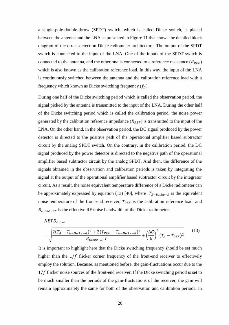
a single-pole-double-throw (SPDT) switch, which is called Dicke switch, is placed
between the antenna and the LNA as presented in Figure 11 that shows the detailed block
diagram of the direct-detection Dicke radiometer architecture. The output of the SPDT
switch is connected to the input of the LNA. One of the inputs of the SPDT switch is
connected to the antenna, and the other one is connected to a reference resistance (𝑅𝑅𝐸𝐹)
which is also known as the calibration reference load. In this way, the input of the LNA
is continuously switched between the antenna and the calibration reference load with a
frequency which known as Dicke switching frequency (𝑓𝐷).
During one half of the Dicke switching period which is called the observation period, the
signal picked by the antenna is transmitted to the input of the LNA. During the other half
of the Dicke switching period which is called the calibration period, the noise power
generated by the calibration reference impedance (𝑅𝑅𝐸𝐹) is transmitted to the input of the
LNA. On the other hand, in the observation period, the DC signal produced by the power
detector is directed to the positive path of the operational amplifier based subtractor
circuit by the analog SPDT switch. On the contrary, in the calibration period, the DC
signal produced by the power detector is directed to the negative path of the operational
amplifier based subtractor circuit by the analog SPDT. And then, the difference of the
signals obtained in the observation and calibration periods is taken by integrating the
signal at the output of the operational amplifier based subtractor circuit by the integrator
circuit. As a result, the noise equivalent temperature difference of a Dicke radiometer can
be approximately expressed by equation (13) [40], where 𝑇𝐸−𝐷𝑖𝑐𝑘𝑒−𝑅 is the equivalent
noise temperature of the front-end receiver, 𝑇𝑅𝐸𝐹 is the calibration reference load, and
𝐵𝐷𝑖𝑐𝑘𝑒−𝑅𝐹 is the effective RF noise bandwidth of the Dicke radiometer.
𝑁𝐸𝑇𝐷𝐷𝑖𝑐𝑘𝑒
= √2(𝑇𝐴 + 𝑇𝐸−𝐷𝑖𝑐𝑘𝑒−𝑅)2 + 2(𝑇𝑅𝐸𝐹 + 𝑇𝐸−𝐷𝑖𝑐𝑘𝑒−𝑅)2
𝐵𝐷𝑖𝑐𝑘𝑒−𝑅𝐹𝜏+ (
Δ𝐺
𝐺)
2
(𝑇𝐴 − 𝑇𝑅𝐸𝐹)2 (13)
It is important to highlight here that the Dicke switching frequency should be set much
higher than the 1/𝑓 flicker corner frequency of the front-end receiver to effectively
employ the solution. Because, as mentioned before, the gain-fluctuations occur due to the
1/𝑓 flicker noise sources of the front-end receiver. If the Dicke switching period is set to
be much smaller than the periods of the gain-fluctuations of the receiver, the gain will
remain approximately the same for both of the observation and calibration periods. In

21
essence, by the Dicke switching technique, the output spectrum of the radiometer is
shifted from DC to the Dicke switching frequency (𝑓𝐷). Therefore, the output signal of
the radiometer, which is a difference of the signals obtained in the observation and
calibration periods, will be not affected by the gain-fluctuations of the front-end receiver
if the physical noise temperature of the calibration reference load (𝑇𝑅𝐸𝐹) is equal to the
antenna noise temperature (𝑇𝐴), as presented in equation (14) where 𝑇𝐷𝑖𝑐𝑘𝑒−𝑆 is the overall
system equivalent noise temperature which is equal to the sum of the antenna noise
temperature (𝑇𝐴) and the equivalent noise temperature of the front-end receiver
(𝑇𝐸−𝐷𝑖𝑐𝑘𝑒−𝑅). As can be seen from the comparison of the NETD equations of the total
power (7) and Dicke radiometers (14), the temperature resolution of the Dicke radiometer
is twice that of the total power radiometer since the effective observation time reduces to
its half (%50 duty cycle). In spite of this penalty factor of 2 in the Dicke radiometer, the
improvement in the NETD performance is very much better than that of the total power
radiometer since it is more than compensated by eliminating the gain-fluctuation term.
𝑁𝐸𝑇𝐷𝐷𝑖𝑐𝑘𝑒 = 2𝑇𝐷𝑖𝑐𝑘𝑒−𝑆√1
𝐵𝐷𝑖𝑐𝑘𝑒−𝑅𝐹𝜏 (14)
The equivalent noise temperature of the front-end receiver of a Dicke radiometer can be
calculated using equation (15), where 𝑇𝐸−𝑆𝑃𝐷𝑇 is the equivalent noise temperature of the
SPDT switch, 𝐺𝑆𝑃𝐷𝑇 is the gain of the SPDT switch, and 𝐺𝐿𝑁𝐴 and is the gain of the LNA
𝑇𝐸−𝐷𝑖𝑐𝑘𝑒−𝑅 = 𝑇𝐸−𝑆𝑃𝐷𝑇 +𝑇𝐸−𝐿𝑁𝐴
𝐺𝑆𝑃𝐷𝑇+
𝑇𝐸−𝑃𝐷
𝐺𝑆𝑃𝐷𝑇𝐺𝐿𝑁𝐴 (15)
Furthermore, the equivalent noise temperature of the front-end receiver of a Dicke
radiometer can be directly found by equation (16), using the noise equivalent power
(𝑁𝐸𝑃𝐷𝑖𝑐𝑘𝑒−𝑅) of the overall front-end receiver circuit that consists of the SPDT switch,
LNA, and the power detector.
𝑇𝐸−𝐷𝑖𝑐𝑘𝑒−𝑅 =𝑁𝐸𝑃𝐷𝑖𝑐𝑘𝑒−𝑅
𝑘√𝐵𝐷𝑖𝑐𝑘𝑒−𝑅𝐹
(16)
The effective RF noise bandwidth of a Dicke radiometer can be calculated by equation
(17) using the pre-detector gain (𝐺𝑝𝑟𝑒−𝑑𝑒𝑡𝑒𝑐𝑡𝑜𝑟).
𝐵𝑅𝐹 =[∫ 𝐺𝑝𝑟𝑒−𝑑𝑒𝑡𝑒𝑐𝑡𝑜𝑟(𝑓)𝑑𝑓
∞
0]
2
∫ 𝐺𝑝𝑟𝑒−𝑑𝑒𝑡𝑒𝑐𝑡𝑜𝑟2 (𝑓)𝑑𝑓
∞
0
(17)

22
Finally, the integrated output signal can be converted to digital form using an ADC and
data acquisition and then processed by a computer or a specific digital signal processor
(DSP). As mentioned for the total power radiometer in Section 2.1.2.1, this radiometer
channel is considered as a single pixel element, and a two-dimensional (2D) images can
be created by using the aforementioned techniques.
2.2. Power Detector
2.2.1 Circuit Design and Implementation
The NETD of a radiometer is determined mainly by the NEP performance of the power
detector. That is why starting with the design of the power detector to build a radiometer
can be considered as a good starting point. The power detector produces an output voltage
proportional to the input power. The relationship between the input power and the output
voltage should be as linear as possible to detect the power difference at the input
accurately. Therefore, the power detector should be operated in the square-law region.
The circuit schematic of the designed power detector is shown in Figure 14. A cascode
like configuration was utilized for the first time beyond 100 GHz to perform power
detection operation, and its NEP performance was analyzed for the first time for SiGe
HBT technology. The CE transistor (Q1) produces a second-order DC current response
to the input power. The first order response is eliminated by the shunt capacitor of 340 fF
placed between the CE (Q1) and CB (Q2) transistors. Moreover, since this shunt capacitor
acts almost perfect AC grounding path for operating frequency range, the input
impedance of the CE transistor is isolated from the rest of the circuit. The CB transistor
(Q2) can be considered as a unity gain current buffer. Although the output noise voltage
is slightly increased by the CB transistor (Q2), it makes easier for the CE transistor (Q1)
to remain in the forward active regime since the CB transistor (Q2) keeps the collector
voltage of the CE (Q1) transistor as constant as possible. This improvement is presented
in Figure 15 using the same load resistor (100 kΩ) and same bias voltage values. As can
be seen from the figure, although the CE transistor (Q1) starts to operate in the saturation
region for input powers larger than -24 dBm when operating stand-alone, it is kept staying
in the forward-active region when configured with the CB transistor (Q2). In addition, it
has been shown that a SiGe HBT biased with a forced emitter current can have a collector-
emitter breakdown voltage (BVCEO) that is twice as high as its nominal value [41].
Thence, the supply voltage VCC of the power detector can be set to higher voltage values,

23
and it makes possible use of larger load resistor which results with larger responsivity and
better NEP performance as will be explained later in this section.
In the cascode topology, the collector current of the whole circuit is determined by the
CE transistor (Q1) since the current gain of the CB transistor is equal to one. Thus,
assuming that the input signal at the base of the CE transistor is a sinusoidal-wave with
an amplitude of Vin, and a frequency of f, the collector current (Ic) can be expressed by
equation (18) neglecting early voltage effect; where Is is the saturation current, VBE is the
base-emitter bias voltage of the CE transistor (Q1), and VT is the thermal voltage which
equals to kT/q. It should be noted that equation (18) is valid for a transistor operating in
the forward-active region.
Figure 14 Circuit schematic of the D-band power detector (Electrical lengths of the
transmission lines are given for 140 GHz).
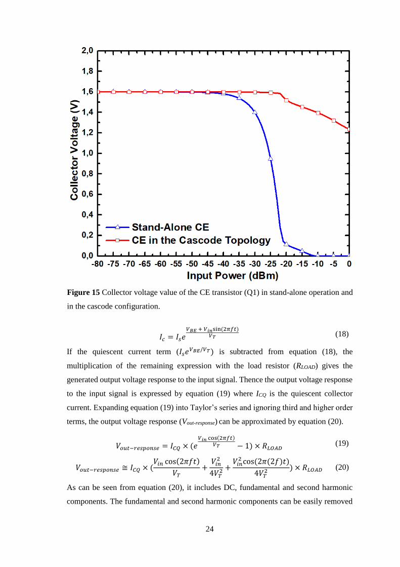
24
𝐼𝑐 = 𝐼𝑠𝑒𝑉𝐵𝐸 + 𝑉𝑖𝑛sin (2𝜋𝑓𝑡)
𝑉𝑇 (18)
If the quiescent current term (𝐼𝑠𝑒𝑉𝐵𝐸/𝑉𝑇) is subtracted from equation (18), the
multiplication of the remaining expression with the load resistor (RLOAD) gives the
generated output voltage response to the input signal. Thence the output voltage response
to the input signal is expressed by equation (19) where ICQ is the quiescent collector
current. Expanding equation (19) into Taylor’s series and ignoring third and higher order
terms, the output voltage response (Vout-response) can be approximated by equation (20).
𝑉𝑜𝑢𝑡−𝑟𝑒𝑠𝑝𝑜𝑛𝑠𝑒 = 𝐼𝐶𝑄 × (𝑒𝑉𝑖𝑛 cos(2𝜋𝑓𝑡)
𝑉𝑇 − 1) × 𝑅𝐿𝑂𝐴𝐷 (19)
𝑉𝑜𝑢𝑡−𝑟𝑒𝑠𝑝𝑜𝑛𝑠𝑒 ≅ 𝐼𝐶𝑄 × (𝑉𝑖𝑛 cos(2𝜋𝑓𝑡)
𝑉𝑇+
𝑉𝑖𝑛2
4𝑉𝑇2 +
𝑉𝑖𝑛2 cos (2𝜋(2𝑓)𝑡)
4𝑉𝑇2 ) × 𝑅𝐿𝑂𝐴𝐷 (20)
As can be seen from equation (20), it includes DC, fundamental and second harmonic
components. The fundamental and second harmonic components can be easily removed
Figure 15 Collector voltage value of the CE transistor (Q1) in stand-alone operation and
in the cascode configuration.

25
using a shunt-capacitor at the output of the CE transistor, as employed in Figure 14.
Therefore, the DC voltage response (Vout-response-dc) to the input signal can be
approximately expressed by equation (21). The DC output voltage response is
proportional to the square of the input voltage of the transistor. This also points why the
power detection operation is called as “square-law operation”.
𝑉𝑜𝑢𝑡−𝑟𝑒𝑠𝑝𝑜𝑛𝑠𝑒−𝑑𝑐 ≅ 𝐼𝐶𝑄 × (𝑉𝑖𝑛
2
4𝑉𝑇2) × 𝑅𝐿𝑂𝐴𝐷 (21)
Rewriting equation (21) in terms of the available power from source (𝑃𝑎𝑣𝑠), the impedance
of the source (𝑍𝑠) and the input impedance (𝑍𝑖𝑛), the voltage response at the output (Vout-
response-dc) to the input signal can be expressed by equation (22). The validity of equation
(22) is demonstrated by comparison of the calculated and simulated result, as shown in
Figure 16. The slight difference between the calculated and simulated curves can be
attributed to the non-idealities of the I-V characteristics of the transistors.
𝑉𝑜𝑢𝑡−𝑟𝑒𝑠𝑝𝑜𝑛𝑠𝑒−𝑑𝑐 ≅ 𝐼𝐶𝑄 × (8𝑃𝑎𝑣𝑠𝑅𝑒𝑍𝑠 |
𝑍𝑖𝑛
𝑍𝑠 + 𝑍𝑖𝑛|
2
4𝑉𝑇2 ) × 𝑅𝐿𝑂𝐴𝐷
(22)
The responsivity of power detector, which defined as the change in dc output voltage per
unit input power, is one of the most crucial performance metrics for radiometer systems.
The responsivity (𝛽) can be calculated by dividing equation (22) by the available source
power (𝑃𝑎𝑣𝑠), as presented in equation (23) where 𝛼 is a function of the input impedance
(𝑍𝑖𝑛) and the impedance of the signal source (𝑍𝑠) (𝛼 = 𝑅𝑒𝑍𝑠|𝑍𝑖𝑛/(𝑍𝑠 + 𝑍𝑖𝑛)|2). As
indicated in equation (23), the responsivity (𝛽) of power detector is proportional to the
quiescent current (ICQ) and the load resistor (RLOAD) of the power detector, and inversely
proportional to the square of its operating temperature. It is quite worth to say here that
the analysis for the responsivity presented above is valid under the condition that the input
power is small enough to guarantee that the transistors are operating in the forward-active
region.
𝛽 = 𝑉𝑜𝑢𝑡−𝑟𝑒𝑠𝑝𝑜𝑛𝑠𝑒−𝑑𝑐
𝑃𝑎𝑣𝑠≅ 𝐼𝐶𝑄 (
8𝑅𝑒𝑍𝑠 |𝑍𝑖𝑛
𝑍𝑠 + 𝑍𝑖𝑛|
2
4𝑉𝑇2 ) 𝑅𝐿𝑂𝐴𝐷 = 𝛼
𝐼𝐶𝑄
𝑉𝑇2 𝑅𝐿𝑂𝐴𝐷 (23)

26
The NEP (in 𝑊/𝐻𝑧1/2) of a power detector, which is defined as the ratio of the output
noise voltage spectral density (𝑆𝑣𝑜) (in 𝑉/𝐻𝑧1/2) to the responsivity (𝛽) as indicated in
equation (24), is considered as the obvious figure-of-merit of the power detectors in the
passive imaging systems.
𝑁𝐸𝑃 = 𝑆𝑣𝑜
𝛽 (24)
The NEP points out the minimum input power that can be detected. In other words, the
NEP defines the required minimum input power to obtain a unity signal-to-noise ratio at
the output of the power detector. In order to find out the expression of the NEP of a power
detector, we first need to figure out the output noise power spectral density (𝑉𝑛2 /Δ𝑓) of
the power detector. There are four major noise sources at low frequencies in a SiGe HBT:
the flicker noise (1/𝑓), the thermal noise of the parasitic base resistance (𝑉𝑟𝑏𝑛), the base
shot noise (𝑖𝑏𝑛), and the collector shot noise (𝑖𝑐𝑛). The flicker noise (or 1/𝑓 noise) can be
ignored since the circuit will be modulated at the Dicke switching frequency (10 kHz)
Figure 16 Output voltage response to the available source power.

27
which is far above the 1/𝑓 corner frequency illustrated in Figure 17 that shows the low-
frequency output noise voltage spectral density of the designed circuit. The low-
frequency small-signal equivalent circuit of the cascode configuration based power
detector including the major noise sources is shown in Figure 18. It should not be
forgotten here that the base-emitter and collector output resistances (𝑟𝑏𝑒 and 𝑟𝑜) represent
real parts of impedances without having thermal noise. The base-emitter, collector-base,
collector-emitter, and collector-substrate capacitances can be ignored because they
behave as open circuits in the frequency of interest (10 kHz). The total output noise power
spectral density (𝑉𝑛𝑜2 /Δ𝑓) was derived by considering Figure 18. The superposition
theorem was applied to calculate the total output noise power spectral density (𝑉𝑛𝑜2 /Δ𝑓)
since the correlation between the presented noise sources can be ignored in the frequency
domain of interest. The output noise power spectral density terms due to each noise source
were derived, as presented in equations (25(32), where k is the Boltzmann constant, 𝐼𝐵𝑄
and 𝐼𝐶𝑄 are quiescent currents. The total output noise power spectral density (𝑉𝑛𝑜2 /Δ𝑓) is
equal to the sum of all these terms. When the parameters in these terms are roughly
evaluated, it is clear that the collector shot noise of the CE transistor (𝑖𝑐𝑛1) and the thermal
noise of the load resistor (𝑣𝑙𝑜𝑎𝑑) are dominant. Thus, the total output noise power spectral
density (𝑉𝑛𝑜2 /Δ𝑓) can be simplified to equation (33).
𝑉𝑛𝑜2
(𝑅𝑠) /Δ𝑓 ≅ 4𝑘𝑇𝑅𝑆 × (
|𝑅𝐵𝐸1|
|𝑅𝐵𝐸1 + 𝑟𝑏𝑛1 + 𝑅𝑠|)
2
× 𝑔𝑚12 × 𝑅𝐿𝑂𝐴𝐷
2 (25)
𝑉𝑛𝑜2
(𝑟𝑏𝑛1) /Δ𝑓 ≅ 4𝑘𝑇𝑟𝑏𝑛1 × (
|𝑅𝐵𝐸1|
|𝑅𝐵𝐸1 + 𝑟𝑏𝑛1 + 𝑅𝑠|)
2
× 𝑔𝑚12 × 𝑅𝐿𝑂𝐴𝐷
2 (26)
𝑉𝑛𝑜2
(𝐼𝑏𝑛1) /Δ𝑓 ≅ 2𝑞𝐼𝐵𝑄1 × (
|𝑟𝑏𝑛1 + 𝑅𝑠|
|𝑅𝐵𝐸1 + 𝑟𝑏𝑛1 + 𝑅𝑠|)
2
× 𝑅𝐵𝐸12 × 𝑔𝑚1
2 × 𝑅𝐿𝑂𝐴𝐷2 (27)
𝑉𝑛𝑜2
(𝐼𝑐𝑛1) /Δ𝑓 ≅ 2𝑞𝐼𝐶𝑄 × 𝑅𝐿𝑂𝐴𝐷
2 (28)
𝑉𝑛𝑜2
(𝑟𝑏𝑛2) /Δ𝑓 ≅ 4𝑘𝑇𝑟𝑏𝑛2 × (
|𝑔𝑚2𝑅𝐵𝐸2|
|𝑟𝑜1(1 + 𝑔𝑚2𝑅𝐵𝐸2)|)
2
× 𝑅𝐿𝑂𝐴𝐷2 (29)
𝑉𝑛𝑜2
(𝐼𝑏𝑛2) /Δ𝑓 ≅ 2𝑞𝐼𝐵𝑄2 × (
|𝑔𝑚2𝑟𝑏𝑛2𝑅𝐵𝐸2|
|𝑟𝑏𝑛2 + (𝑟𝑜1(1 + 𝑔𝑚2𝑅𝐵𝐸2)|)
2
× 𝑅𝐿𝑂𝐴𝐷2 (30)
𝑉𝑛𝑜2
(𝐼𝑐𝑛2) /Δ𝑓 ≅ 2𝑞𝐼𝐶𝑄2 × (
1
|1 + 𝑔𝑚2𝑅𝐵𝐸2|)
2
× 𝑅𝐿𝑂𝐴𝐷2 (31)

28
𝑉𝑛𝑜2
(𝑅𝐿𝑂𝐴𝐷) /Δ𝑓 ≅ 4𝑘𝑇𝑅𝐿𝑂𝐴𝐷 (32)
𝑉𝑛𝑜2 /Δ𝑓 = 2𝑞𝐼𝐶𝑄𝑅𝐿𝑂𝐴𝐷
2 + 4𝑘𝑇𝑅𝐿𝑂𝐴𝐷 (33)
As mentioned earlier, the NEP (in 𝑊/𝐻𝑧1/2) of a power detector is defined as the ratio
of the output noise voltage spectral density (𝑆𝑣𝑜) (in 𝑉/𝐻𝑧1/2) to the responsivity (𝛽). If
the square root of the total output noise power spectral density (𝑉𝑛𝑜2 /Δ𝑓) (33) and the
responsivity (𝛽) (23) expressions are substituted into the equation of the NEP (24), then
the NEP can be expressed by equation (34).
𝑁𝐸𝑃 = 𝑆𝑣𝑜
𝛽=
√𝑉𝑛𝑜2
Δ𝑓
𝛽=
√2𝑞𝐼𝐶𝑄𝑅𝐿𝑂𝐴𝐷2 + 4𝑘𝑇𝑅𝐿𝑂𝐴𝐷
𝛼𝐼𝐶𝑄
𝑉𝑇2 𝑅𝐿𝑂𝐴𝐷
=𝑉𝑇
2
𝛼√
2𝑞
𝐼𝐶𝑄+
4𝑘𝑇
𝐼𝐶𝑄2 𝑅𝐿𝑂𝐴𝐷
(34)
Figure 17 Output noise voltage spectral density of the designed power detector
(schematic based result).

29
Figure 18 Low frequency small-signal equivalent circuit of the cascode configuration.
Figure 19 NEP and responsivity (𝛽) versus load resistance (𝑅𝐿𝑂𝐴𝐷) (Loss due to the
impedance mismacth between the input of the transistor and the source was de-embedded)
(@140 GHz).

30
As can be seen from (34), the NEP performance of a power detector can be improved by
increasing the load resistance (𝑅𝐿𝑂𝐴𝐷) and the quiescent current (𝐼𝐶𝑄). But this
improvement is limited due to two reasons. Firstly, higher quiescent current (𝐼𝐶𝑄) and
larger load resistance (𝑅𝐿𝑂𝐴𝐷) will cause a significant voltage drop between the supply
voltage (𝑉𝐶𝐶) and the collector of the CB transistor (Q2), and it would saturate the both
transistors. Even though this problem will be able to be solved by increasing the supply
voltage (𝑉𝐶𝐶) to a voltage level that will not damage the transistors, a small increase of
the amplitude of the input signal (𝑉𝑖𝑛) would cause a significant voltage drop again. The
second reason is that the maximum current values which can flow through high value
resistances in semiconductor technologies are very limited. For the used semiconductor
process (IHP’s SG13G2), the highest value resistor material, which is made by p-doped
gate polysilicon, can drain a maximum 0.15 mA current, for a width of 0.5 𝜇m.
Figure 20 NEP and responsivity (𝛽) versus the base-emitter voltage of the CE transistor
(Loss due to the impedance mismacth between the input of the transistor and the source
was de-embedded) (@140 GHz).

31
The dependence of the NEP performance on the load resistance (𝑅𝐿𝑂𝐴𝐷) is shown in
Figure 19 for same quiescent current and the same quiescent voltage value at the collector
of the CB transistor. As expected from the equations derived for the NEP and the
responsivity (𝛽), the performance of the power detector circuit increases with increasing
load resistance (𝑅𝐿𝑂𝐴𝐷). Figure 20 shows the dependence of the NEP performance on the
quiescent current (𝐼𝐶𝑄) while using same load resistance (𝑅𝐿𝑂𝐴𝐷) and having the same
quiescent voltage value at the collector of the CB transistor. The quiescent current (𝐼𝐶𝑄)
was increased up to the allowed maximum current value for the used resistor material.
The trade-offs and aforementioned limitations were carefully evaluated, and a higher load
resistor (𝑅𝐿𝑂𝐴𝐷) was chosen instead of higher quiescent current value (𝐼𝐶𝑄) to minimize
NEP of the power detector. In order to improve NEP, the responsivity (𝛽) of the circuit
should be increased, i.e. the second-order dc response of the CE transistor (Q1) should be
enhanced as possible. Therefore, the transistor size should be as small as possible, as
verified by the simulation result shown in Figure 21.
Figure 21 NEP and responsivity (𝛽) versus the emitter length of the transistor (Loss due
to the impedance mismacth between the input of the transistor and the source was
deembedded) (@140 GHz)

32
The available power at the input of the power detector should be transmitted to the input
of the first transistor (Q1) without having losses due to the impedance mismatching to not
degrade the responsivity (𝛽). Thus, the impedance matching between the input of the
power detector and the input of the first transistor (Q1) have a significant effect on the
responsivity (𝛽), so also on the NEP performance of the power detector. It is very
important to have a low NEP value across a broadband frequency range to mimize the
NETD value of the radiometer. As explained before, if the transistor size is set to
minimum value, the NEP performance is obtained. But this results in narrowband
impedance matching because of the very large input impedance of the transistor.
After all these design guidelines had been taken into account and evaluated, the quiescent
current (𝐼𝐶𝑄) was set to 50 μA, a 100 kΩ load resistance (𝑅𝐿𝑂𝐴𝐷) was used, and the emitter
size of the transistor was chosen to be 2x unit.
The transmission line based T-type matching network was used to perform the impedance
matching between the input of the power detector circuit and the input of the first
transistor (Q1). All the transmission lines were implemented as microstrip lines with Top
Metal 2 – Metal 1 configuration and all of them were meandered to reduce the chip area.
A MIM capacitor of 200 fF was employed to perform DC blocking, as well as to
contribute to the input impedance matching slightly. Parasitic capacitance due to the RF
pad was not included in the input impedance matching. Instead, a Through-Reflect-Line
(TRL) de-embedding fixture was utilized to de-embed the effect of RF-pad and shift the
reference plane. The collector of the CE transistor (Q1) was shunted by a MIM capacitor
of 340 fF to remove the fundamental signal component, and to isolate the input impedance
of the CE transistor (Q1) from the rest of the circuit. The load resistance of 100 kΩ was
realized by a p-doped gate polysilicon. Full-chip electromagnetic (EM) simulations were
performed by ADS Momentum. The 3D layout view taken from the electromagnetic
simulation setup of the D-band power detector is shown in Figure 22.
An ideal bias network should provide a very good AC grounding for all frequencies, but
this is not practically possible. For this reason, at least, the bias line network should
provide a very good AC grounding for the frequency range of interest. A capacitor has a
self-resonance frequency (SRF) depending on its geometrical structure and its size. For
instance, the SRF of the 340 fF capacitor which was on the base-bias line is 140 GHz in
the used process technology (IHP’s SG13G2), and it can just provide an acceptable AC

33
grounding between 100 GHz and 180 GHz. Another bypass capacitor should be placed
on the base-bias line to ground smaller frequencies, but if it is connected in parallel to the
first bypass capacitor, their parasitics will be added up, and it would result in unexpected
and undesired frequency response. Therefore, a small value resistor should be placed on
the bias line, between these two-bypass capacitors. That is why a double RC section was
utilized on the base-bias line, as presented in Figure 14.
2.2.2 Simulation and Measurement Results
The chip microphotograph of the designed power detector is shown in Figure 23. The
effective chip area excluding the pads and de-embedding lines is 0.18 mm2, and the total
area of the integrated circuit is 0.32 mm2. The total quiescent power consumption is 0.43
mW.
S-parameters of the power detector were measured by Keysight N5224A PNA whose
frequency extended to 110-170 GHz using a Virginia Diodes Inc. (VDI) WR6.5
frequency extension module. One-port SOL calibration was performed by an ISS from
Cascade-Microtech to move the reference plane to the probe tip. The power at the probe
Figure 22 3D layout view taken from the electromagnetic simulation setup of the D-band
power detector.

34
tip was set to be less than -40 dBm along the D-band to guarantee that the power detector
is operating in the square-law region. Later, one-port SOL de-embedding algorithm on
Cascade WinCal XE software was performed using the data obtained from on-chip de-
embedding structures to remove the parasitic effects of the RF pad. Figure 24 shows the
simulated and measured s-parameters of the power detector. As can be seen from Figure
24, there is a quite good agreement between the simulated and measured s-parameter
results. The return loss of the power detector is better than 10 dB between 123 and 170
GHz with the RF-pad, and better than 10 dB along the D-band without the RF-pad.
Figure 23 Chip microphotograph of the designed power detector (0.53 mm × 0.61 mm).

35
An experimental test setup, which is shown in Figure 25, was set to measure the 1/f
flicker noise of the power detector. The input of the power detector was externally
terminated by a WR6.5 waveguide 50Ω load. The noise voltage at the output of the power
detector was amplified by an external low-noise pre-amplifier (SR-550) and then
measured by Keysight 35670A dynamic signal analyzer between 1 Hz and 10 kHz. Later,
the gain of SR-550 was de-embedded from the measurement.
Figure 24 Simulated and measured s-parameter results of the power detector.
Figure 25 Experimental setup for the measurement of the 1/f flicker noise of the power
detector.

36
The measured low-frequency output noise voltage spectral density of the power detector
is presented in Figure 26. The output noise voltage spectral density is almost constant
(620 nV/√Hz) above 2 kHz which can be also considered as the 1/f corner frequency of
the power detector. As mentioned earlier, the Dicke switching frequency should be set to
be far away from 2 kHz. Therefore, the output noise voltage spectral density (𝑆𝑣𝑜) was
taken as 620 𝑛𝑉/√𝐻𝑧 in the noise equivalent power (NEP) calculations.
Figure 26 Measured 1/𝑓 flicker noise of the power detector.
Figure 27 Experimental test setup for the measurement of the output voltage waveform
and the responsivity of the power detector.

37
Figure 28 Measured output voltage waveform of the power detector (@140 GHz).
Figure 29 Simulated and measured responsivity of the power detector.

38
Figure 27 shows the experimental test setup which was used to observe the output voltage
waveform and to measure the responsivity of the power detector. It is very important to
know exactly the power at the probe tip at the input of the power detector to measure the
responsivity correctly. Therefore, first, the conversion loss between the “a” port of the D-
band directional coupler and the IF port (“b”) of the D-band direct down-conversion
mixer was measured by connecting a D-band power meter to the “a” port of the D-band
directional coupler. It was verified that this conversion loss is constant for all power levels
that would be used during the responsivity measurements. Second, a second probe, which
is identical to the presented probe (at left in the figure), was connected to the D-band
power meter, and in this way, the total insertion loss of the two s-bend waveguides and
two probes was measured using a small through-line on the ISS. By dividing this value
by half, the insertion loss between the “a” port of the D-band directional coupler and the
probe tip was found. The insertion losses figured out above were taken into account while
measuring the responsivity of the power detector.
Figure 30 Simulated and measured NEP of the power detector.

39
An input signal to the input of the power detector which was AM modulated at 10 kHz
with a modulation depth of %100 was applied to emulate the impact of the Dicke switch.
Figure 28 shows the measured output voltage waveform of the power detector while the
power of the input signal varies from -34.2 dBm to -60 dBm at 140 GHz. As mentioned
earlier and presented in equation (23), the responsivity can be calculated by dividing the
change in dc output voltage by the change in input power. This procedure was repeated
with 10 GHz step-size between 110 and 170 GHz. The simulated and measured
responsivity results of the power detector are presented in Figure 29. As can be seen from
the figure, the measured curve matches well with the simulated result. The measured peak
responsivity value of the power detector is about 883 kV/W at 130 GHz. It gradually
decreases after 130 GHz, and its minimum value is about 373 kV/W at 170 GHz.
The NEP of the power detector was calculated by dividing the output noise voltage
spectral density by the responsivity. Figure 30 shows the simulated and measured NEP
of the power detector. The measured NEP is better than 1 𝑝𝑊/𝐻𝑧1/2 over 110-150 GHz
frequency range, and its minimum value is about 0.7 𝑝𝑊/𝐻𝑧1/2 at 130 GHz. The slight
discrepancy between the simulation and measurement results above 120 GHz can be
attributed to that the measured responsivity value is slightly better than the simulation in
at the same frequency range.
2.2.3 Comparison
The performance comparison of the power detector with previously reported D-band
power detectors implemented in silicon technologies is summarized in Table 3. The NEP
performance of a power detector is the most important parameter, which is also
considered as the figure-of-merit (𝐹𝑜𝑀) of the power detectors in the passive imaging
systems. The designed power detector achieves the best noise equivalent power
performance compare to previously reported D-band power detectors implemented in
silicon technologies. Moreover, the designed power detector has the highest responsivity
among the other silicon-based studies in the literature, thanks to higher value load resistor.
Even though the use of high resistance results in a lower power compression point of
approximately -30 dBm, it is not a priority performance criterion for the passive imaging
applications. These results point that the D-band power detector shows the state-of-the-
art performance and emphasize the suitability of the power detector for mm-wave passive
imaging systems to achieve excellent NETD performance.

40
Table 3 Summary of performance comparison of the D-band power detector with
previously reported D-band power detectors implemented in silicon technologies.
Technology
NEP
(𝒑𝑾/𝑯𝒛𝟏/𝟐)
Responsivity
(𝒌𝑽/𝑾)
RLOAD
(𝒌Ω)
S11
<-10
dB
(𝑮𝑯𝒛)
Area
(𝒎𝒎𝟐)
[42] 45nm CMOS
SOI 8 3 1
167-
194 0.20
[43] 90nm SiGe
BiCMOS 2.7 10 1
125-
170 0.21
[44] 90nm SiGe
BiCMOS 0.7 11 0.6
145-
170 0.05*
[44] 90nm SiGe
BiCMOS 1.25 14.5 1 N/A 0.02*
[45] 0.13𝜇m SiGe
BiCMOS 10 10 1 - N/A
This
Work
0.13𝝁m SiGe
BiCMOS 0.7 883 100
110-
170 0.18*
* Excluding the pads
2.3. Low-Noise Amplifier
2.3.1 Circuit Design and Implementation
The circuit schematic of the designed LNA is shown in Figure 31. The designed LNA
consists of four cascode stages. In order to reduce the noise contribution of the CB
transistor, a shunt inductor was placed between the CE and CB transistors, which is based
on the technique proposed in [46] for WLAN applications and CMOS technology. The
effect of this shunt inductor on the noise figure performance of the cascode configuration
was analyzed for the SiGe HBT technology. Furthermore, a Butterworth approximation
based staggered tuning technique was utilized to enhance the bandwidth and improve the
gain flatness of the LNA.
The amplitude of the signal collected by the antenna is expected to be very low, around -
100 dBm, as analyzed in Section 2.1. A high-gain LNA is required to amplify the signal
collected by the antenna and to suppress the noise of the power

41
Figure 31 Circuit schematic of the designed D-band LNA (Electrical lengths of the
transmission lines are given for 140 GHz).

42
detector. Assuming a bandwidth of 40 GHz, an integration time of 30 ms, a NEP of 0.8
𝑝𝑤/𝐻𝑧1/2 for the power detector, and an insertion loss of 2.5 dB for the SPDT switch,
the dependence of the NETD performance of the Dicke radiometer architecture on the
gain and noise figure of the LNA is demonstrated in Figure 32. As could be seen in the
Figure 32, the noise figure of the LNA should be as low as possible, and the LNA should
have a gain of at least 30 dB to suppress the noise of the power detector enough under
aforementioned assumptions. The MATLAB code that was used to figure out the effect
of the gain and noise figure of the LNA on the NETD of the radiometer is given in
Appendix A.
Figure 32 Calculated NETD versus the gain of the LNA for various NF values.
Figure 33 High-frequency small-signal equivalent circuit of the cascode topology
including major noise sources.

43
The CE topology comes out with better noise performance while the cascode
configuration comes to the forefront with higher gain performance. The total noise figures
of the cascaded two identical stages for both CE and cascode topologies were calculated
to figure out which one is appropriate to obtain better noise figure performance, assuming
that each stage provides its maximum available gain and minimum noise figure values
and they are operating at the optimum bias point for minimum noise figure without
trading off too much gain. The result of this calculation is that the gain of the CE is not
enough to suppress the following stage. Therefore, it was decided to use the cascode
configuration. Ulusoy et al. [47] presented a gain-boosting technique to enhance the gain
performance of the SiGe HBT cascode configuration operating at D-band. This gain-
boosting technique can be used to enhance the gain so that the noise contribution from
the following stages can be suppressed better. However, it does not cope with the noise
contribution of the CB transistor which leads to trouble in terms of the noise figure,
especially for above 100 GHz. In order to figure out how to reduce the noise contribution
of the CB transistor, the noise figure of the cascode topology was analyzed including the
major noise sources and parasitics in a SiGe HBT.
There are three major noise sources at high-frequencies in a SiGe HBT: the thermal noise
of the parasitic base resistance (𝑉𝑟𝑏𝑛), the base shot noise (𝑖𝑏𝑛), and the collector shot
noise (𝑖𝑐𝑛). The high-frequency small-signal equivalent circuit of the cascode
configuration including the major noise sources is shown in Figure 33. It should be
highlighted here that the base-emitter and collector output resistances (rbe and 𝑟𝑜)
represent real parts of impedances without having thermal noise and, the collector-base
capacitance was omitted for simplification. In Figure 34, Cx represents all parasitic
capacitances between the node-X and the ground such as the collector-emitter and
collector-substrate capacitances of the CE transistor, and the base-emitter and emitter-
substrate capacitances of the CB transistor.
The method presented in [48] was used to derive the noise factor equation of the cascode
topology. The superposition theorem was applied to calculate the total output noise
current power spectral density (𝐼𝑛𝑜2 /Δ𝑓) since the correlation between the presented noise
sources could be ignored for simplification. The output noise current power spectral
density terms due to each noise source were derived by considering Figure 33 and Figure
34, as presented in equations (35-(41), where k is the Boltzmann constant, T is the

44
temperature, 𝐼𝐵𝑄 is the quiescent base current, 𝐼𝐶𝑄 is the quiescent collector current, and
𝑅𝑠 is the source resistance. The total output noise current power spectral density (𝐼𝑛𝑜2 /Δ𝑓)
is equal to the sum of all these terms. Consequently, the noise factor equation of the
conventional cascode topology (𝐹𝑎) can be found out by dividing the total output noise
current power spectral density (𝐼𝑛𝑜2 /Δ𝑓) by the output noise current power spectral density
due to the source (𝑖𝑛𝑜(𝑠𝑜𝑢𝑟𝑐𝑒)2 /Δ𝑓), as presented in equation (42). At this step, the noise
factor terms were called like as shown in equation (42) to highlight the parts related with
the capacitance 𝐶𝑥 in order to focus its effect on the noise factor.
𝐹𝑟𝑏𝑛1, 𝐹𝑖𝑏𝑛1
, 𝐹𝑖𝑐𝑛1, 𝐹𝑟𝑏𝑛2
, 𝐹𝑖𝑏𝑛2, and 𝐹𝑖𝑐𝑛2
are the noise factor terms due to the thermal
noise voltage of the parasitic base resistances and the shot noise currents of the CE and
CB transistor, respectively. As can be seen from equation (42), the noise contribution of
the collector shot noise of the CB transistor escalates as frequency increases, and the
capacitance 𝐶𝑥 has a significant contribution to this undesired effect.
𝐼𝑛𝑜2
(𝑠𝑜𝑢𝑟𝑐𝑒) /Δ𝑓 ≅ 4𝑘𝑇𝑅𝑆 × (
|𝑍𝜋1|
|𝑅𝑠+𝑍𝜋1|)
2
× 𝑔𝑚12 × (
𝑔𝑚2
|𝑔𝑚2+1
𝑍𝑥|)2 (35)
𝐼𝑛𝑜2
(𝑟𝑏𝑛1) /Δ𝑓 ≅ 4𝑘𝑇𝑟𝑏𝑛1 × (
|𝑍𝜋1|
|𝑅𝑠+𝑍𝜋1|)
2
× 𝑔𝑚12 × (
𝑔𝑚2
|𝑔𝑚2+1
𝑍𝑥|)2 (36)
Figure 34 Conventional cascode topology (left) and modified cascode topology with the
shunt-inductor 𝐿𝑥 (right).

45
𝐼𝑛𝑜2
(𝐼𝑏𝑛1) /Δ𝑓 ≅ 2𝑞𝐼𝐵𝑄1 × (
𝑅𝑠
|𝑅𝑠+𝑍𝜋1|)
2
× |𝑍𝜋1|2 × 𝑔𝑚12 × (
𝑔𝑚2
|𝑔𝑚2+1
𝑍𝑥 |)2 (37)
𝐼𝑛𝑜2
(𝐼𝑐𝑛1) /Δ𝑓 ≅ 2𝑞𝐼𝐶𝑄 × (
𝑔𝑚2
|𝑔𝑚2 +1
𝑍𝑥 |
)2 (38)
𝐼𝑛𝑜2
(𝑟𝑏𝑛2) /Δ𝑓 ≅ 4𝑘𝑇𝑟𝑏𝑛2 × (
|𝑔𝑚2𝑍𝑥|
|(𝑟𝑜1(1 + 𝑔𝑚2𝑍𝑥)|)
2
(39)
𝐼𝑛𝑜2
(𝐼𝑏𝑛2) /Δ𝑓 ≅ 2𝑞𝐼𝐵𝑄2 × (
|𝑔𝑚2𝑟𝑏𝑛2𝑍𝑥|
|𝑟𝑏𝑛2 + (𝑟𝑜1(1 + 𝑔𝑚2𝑍𝑥)|)
2
(40)
𝐼𝑛𝑜2
(𝐼𝑐𝑛2) /Δ𝑓 ≅ 2𝑞𝐼𝐶𝑄 × (
1
|1 + 𝑔𝑚2𝑍𝑥|)
2
(41)
𝐹𝑎 ≅ 1 + 𝐹𝑟𝑏𝑛1+ 𝐹𝑖𝑏𝑛1
+ 𝐹𝑖𝑐𝑛1+ 𝐹𝑟𝑏𝑛2
+ 𝐹𝑖𝑏𝑛2+ 𝐹𝑖𝑐𝑛2
(𝜔𝐶𝑥
𝑔𝑚2)
2
(42)
In order to remove the effect of the capacitance 𝐶𝑥 on the noise figure performance, a
shunt inductor 𝐿𝑥 is placed to parallel to 𝐶𝑥 as shown in Figure 4(b). The noise factor
equation of the modified topology with the shunt inductor 𝐿𝑥 was derived by following
the procedure which is presented above for the conventional topology. In this way, the
noise factor of the modified topology (𝐹𝑏) can be expressed by equation (43). As can be
seen from equation (43) if the value of the shunt inductor 𝐿𝑥 is set to resonate with the
capacitance 𝐶𝑥 at the operating frequency, the collector shot noise of the CB transistor
which is the dominant noise source can be removed completely. Figure 35 compares the
simulated maximum stable gain (𝑀𝑆𝐺) and minimum noise figure (𝑁𝐹𝑚𝑖𝑛) of the
conventional and modified cascode topologies (within the typical case). As seen, this
noise reduction technique reduces the minimum noise figure (𝑁𝐹𝑚𝑖𝑛) about 0.5 dB
across whole D-band frequency range. However, the maximum stable gain (𝑀𝑆𝐺)
remains same for both topologies.
𝑭𝒃 ≅ 𝟏 + 𝑭𝒓𝒃𝒏𝟏+ 𝑭𝒊𝒃𝒏𝟏
+ 𝑭𝒊𝒄𝒏𝟏+ 𝑭𝒓𝒃𝒏𝟐
+ 𝑭𝒊𝒃𝒏𝟐+ 𝑭𝒊𝒄𝒏𝟐
(𝟏 − 𝝎𝟐𝑪𝒙𝑳𝒙
𝒈𝒎𝟐𝝎𝑳𝒙)
𝟐
(43)
Another important performance specification that determines the noise equivalent
temperature difference performance of the radiometer is the bandwidth. Bi et al. [49] used
a staggered tuning technique based on Chebyshev distribution at W-band to obtain broad
bandwidth and thus to improve the noise equivalent temperature difference of the
radiometer. Even though it provides broad bandwidth, it has not flat-gain which is another
important performance criterion for the radiometers. The
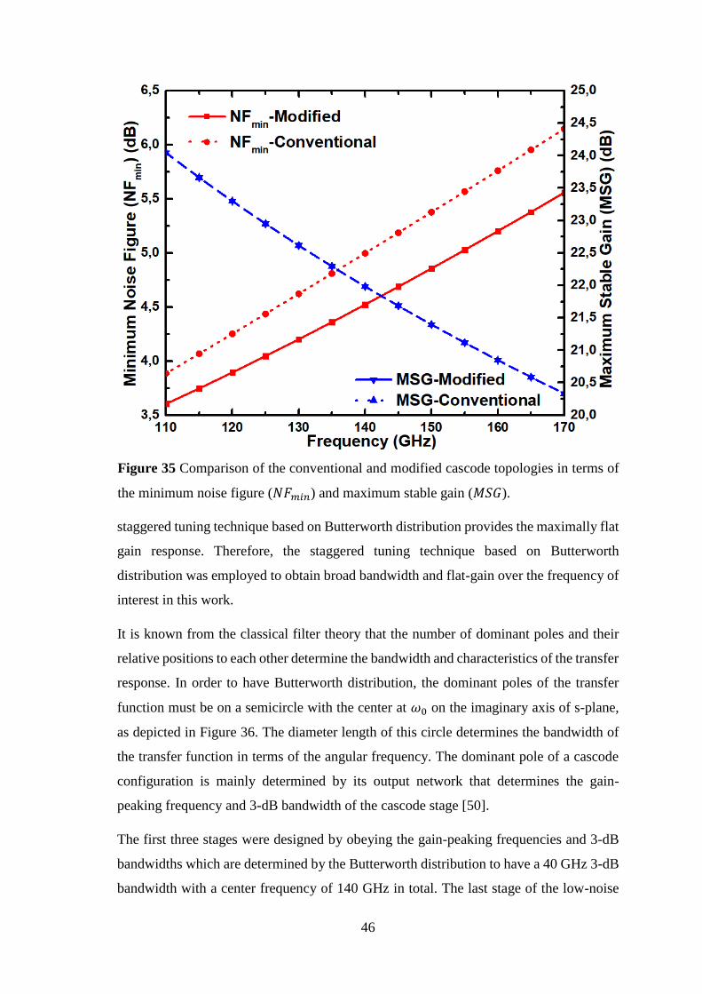
46
staggered tuning technique based on Butterworth distribution provides the maximally flat
gain response. Therefore, the staggered tuning technique based on Butterworth
distribution was employed to obtain broad bandwidth and flat-gain over the frequency of
interest in this work.
It is known from the classical filter theory that the number of dominant poles and their
relative positions to each other determine the bandwidth and characteristics of the transfer
response. In order to have Butterworth distribution, the dominant poles of the transfer
function must be on a semicircle with the center at 𝜔0 on the imaginary axis of s-plane,
as depicted in Figure 36. The diameter length of this circle determines the bandwidth of
the transfer function in terms of the angular frequency. The dominant pole of a cascode
configuration is mainly determined by its output network that determines the gain-
peaking frequency and 3-dB bandwidth of the cascode stage [50].
The first three stages were designed by obeying the gain-peaking frequencies and 3-dB
bandwidths which are determined by the Butterworth distribution to have a 40 GHz 3-dB
bandwidth with a center frequency of 140 GHz in total. The last stage of the low-noise
Figure 35 Comparison of the conventional and modified cascode topologies in terms of
the minimum noise figure (𝑁𝐹𝑚𝑖𝑛) and maximum stable gain (𝑀𝑆𝐺).

47
amplifier was designed to provide wideband output matching without disturbing the
Butterworth characteristic as much as possible. According to Figure 36, the gain-peaking
frequencies of the staggered tuned stages should be 122.7, 140 and 157.3 GHz, and each
stage should have a 3-dB bandwidth of 20 GHz. The gain-peaking frequency of the first
stage was set to 140 GHz to have a noise figure as minimum as possible at the center of
the frequency range. The gain-peaking frequencies of the second and third stages were
optimized to 157.3 and 122.7 GHz, respectively. This order was chosen to avoid a sharp
increase in noise figure as frequency increases. If the second stage had been peaked at
122.7 GHz, the total gain of the first two stages would have been not sufficient to suppress
the noise of the following stages at the higher frequencies since the noise figure naturally
increases with the frequency. Also, the peak-gain of each stage should be the same to
each other to not disturb the Butterworth response. Figure 37 shows the simulated gain of
each stage and the simulated overall gain.
The collector current of the first stage was optimized to obtain a good compromise
between the noise figure (NF) and the maximum available gain (MAG) for the unit
emitter size. The emitter area of the CE transistor (𝑄1) was chosen to enable
Figure 36 Positions of the poles of Butterworth distribution on the s-plane (for 3-poles).

48
simultaneous input power and noise matching. The inductive emitter degeneration
technique was used to keep the peak-gain value same for each stage. If the emitter
degeneration had been used to set the real part of the input impedance to 50Ω as in the
conventional design approach, it would have resulted in different peak-gains for each
stage so that the Butterworth response would have been disturbed. That’s why the
transmission line based T-type matching network was used to perform the input
impedance matching. The electrical lengths and the characteristic impedances of the
transmission lines which are used at the output network were set to have peak-gain at 140
GHz with the calculated 3-dB bandwidth for the Butterworth characteristic. The second
and third stages were designed in the same way but for different peak-gains, and the
collector currents of these stages were increased to allow larger output voltage swing to
achieve better linearity performance.
All the transmission lines were implemented as microstrip lines with Top Metal 2 – Metal
1 configuration and all of them were meandered to reduce the chip area. Parasitic
capacitances due to the RF-pads were not included in the input and output impedance
Figure 37 Schematic based simulations of each stage and overall amplifier.

49
matchings. Instead, a TRL de-embedding fixture was used to de-embed the effect of RF-
pad and shift the reference plane to the input of the LNA. The MIM capacitors were
employed to perform DC-blocking and AC-grounding. The SRF of the 340 fF capacitor
which was used at the bias networks to perform AC-grounding is 140 GHz in the used
process technology (IHP’s SG13G2), and it can just provide an acceptable AC grounding
between 100 GHz and 180 GHz. Another bypass capacitor should be placed on the bias
line to ground smaller frequencies, but if it is connected in parallel to the first bypass
capacitor, their parasitics will be added up, and it would result in unexpected and
undesired frequency response. Therefore, small value resistors were placed on the bias
lines, between two bypass capacitors as shown in Figure 31, and by this way, these R-C
sections on the bias lines help to enhance the low-frequency stability and to improve the
insulation between the stages. ADS momentum was used to perform the full-chip
electromagnetic (EM) simulations. Figure 38 shows the 3D layout view taken from the
electromagnetic simulation setup of the D-band LNA. Isolation walls shown in Figure 38
were employed between the stages to prevent possible unwanted signal leakage between
the stages through the SiO2 layers and the Si-substrate.
2.3.2 Simulation and Measurement Results
The chip microphotograph of the designed D-band LNA is shown in Figure 39. The total
area of the integrated circuit is 1.0 mm2 (1.25 mm × 0.8 mm). The effective chip area,
excluding the pads and lines placed for de-embedding, is 0.6 mm2. The total quiescent
power consumption is 28 mW.
Figure 38 3D layout view taken from EM simulation setup of D-band low noise amplifier.

50
S-parameters of the designed D-band LNA were measured by the Keysight N5224A PNA
whose frequency extended to 110-170 GHz using VDI WR6.5 frequency extension
modules. Two-port SOLT calibration was performed by an ISS from Cascade-Microtech
to move the reference plane to the probe tips. The power at the probe tip was set to be
less than -40 dBm over the D-band to ensure that the designed low-noise amplifier is
operating in the linear region. After that, two-port TRL de-embedding algorithm on
Cascade WinCal XE software was performed using the data obtained from on-chip de-
embedding structures to remove the parasitic effects of the RF pads. The simulated and
measured s-parameter results of the designed low-noise amplifier, including the effects
of the RF-pads, is presented in Figure 40. Figure 41shows the de-embedded simulated
and measured s-parameters of the low-noise amplifier. As can be seen from Figure 41,
there is a quite good agreement between the simulated and measured s-parameter results
of the designed D-band low-noise amplifier. The peak gain of the LNA was measured to
be 33.1 dB at 147 GHz, and the 3-dB bandwidth of the designed LNA is 42 GHz.
Figure 39 Chip microphotograph of the designed D-band LNA (1.25 mm × 0.8 mm).

51
Figure 40 Simulated and measured s-parameter results of the designed LNA, including
the effects of the RF-pads.
Figure 41 De-embedded simulated and measured s-parameter results of the designed
LNA.

52
Figure 42 shows the measured 1-dB compression point. The input referred 1-dB
compression point (𝐼𝑃1𝑑𝐵) was measured to be -37.6 dBm by applying a 140 GHz single-
tone sinusoidal signal to the input of the LNA.
Noise figure measurement of the designed LNA was performed using the experimental
test setup shown in Figure 43. As can be seen from the figure, the input of the LNA was
driven by a D-band ELVA-1 noise source that has an excess-noise-ratio (ENR) of 12-dB.
A D-band faraday isolator was used to avoid the measurement errors that would arise due
to the mismatch between the output of the noise source and the input of the LNA. The
output signal of the LNA was down-converted to an IF frequency by a D-band direct-
down conversion mixer driven by an active multiplication chain configurated with
Agilent E8257C signal generator. The IF signal was amplified by an IF LNA, and then
analyzed by Agilent 8973A noise figure analyzer. Figure 44 shows the simulated and
measured noise figure measurement of the LNA. The extremely low-value points were
not included in the fitted curve. The fitted noise figure is better than 6.1 dB along the D-
band, and the minimum noise figure value of the LNA is 4.8 dB at 127 GHz.
Figure 42 Measured input referred 1-dB compression point of the LNA.

53
Figure 43 Experimental test setup to measure the noise figure of the LNA.
Figure 44 Simulated and measured noise figure performances of the designed LNA.

54
2.3.3 Comparison
The performance comparison of the designed LNA with reported D-band LNAs
implemented in silicon technologies is summarized in Table 4. The figure-of-merit (𝐹𝑜𝑀)
described by equation (44) was used to assess the performance of the LNA.
𝐹𝑜𝑀 = 1000 ×𝐺 ∙ 𝐼𝑃1𝑑𝐵[𝑚𝑊] ∙ 𝐵𝑊3𝑑𝐵[𝐺𝐻𝑧]
(𝐹 − 1) ∙ 𝑃𝐷𝐶[𝑚𝑊] ∙ 𝑓𝑐𝑒𝑛𝑡𝑒𝑟(𝐺𝐻𝑧) (44)
The designed LNA achieves the minimum noise figure, and widest 3-dB bandwidth
compare to previously reported D-band LNAs implemented in silicon technologies.
These results point that the designed D-band LNA shows the state-of-the-art performance,
and it is suitable to be employed in millimeter-wave passive imaging systems to achieve
excellent noise equivalent temperature difference.
Table 4 Summary of performance comparison of the designed D-band LNA with
previously reported D-band LNAs implemented in silicon technologies.
Tech.
Peak
Gain
(dB)
Peaking
Freq.
(GHz)
3-dB
BW
(GHz)
NF
(dB)
IP1dB
(dBm)
PDC
(mW) FoM
[51] 65nm CMOS 13.8 113.7 11.2 10.8 -26.8 40 0.01
[52] 90nm SiGe
BiCMOS 36 138 5.5 N/A N/A 45 --
[43] 90nm SiGe
BiCMOS 30 140 25 6.2 N/A 15 --
[45] 0.13𝜇m SiGe
BiCMOS 35 164 8 11 N/A 92 --
[47] 0.13𝜇m SiGe
BiCMOS 27.5 126 18
5.5-
6.5 -33 12 1.32
[53] 0.13𝜇m SiGe
BiCMOS 24.1 158 40 8.2 -25.9 28 1.07
This
Work
0.13𝜇m SiGe
BiCMOS 33 147 42
4.8-
6.1 -37.6 28 1.78

55
2.4. SPDT Switch
2.4.1 Circuit Design and Implementation
SPDT switch is one of the important sub-blocks in the Dicke radiometer architecture.
Because its insertion loss directly contributes to the overall noise figure of the radiometer
since there is no amplification block before the SPDT switch. At millimeter-wave
frequencies, the quarter-wave shunt switch topology is commonly preferred to avoid the
parasitics of the series devices since these parasitics, especially the parasitic shunt
capacitances, become very costly in terms of the insertion loss performance as frequency
increases. Furthermore, Schmid et al. [54] presented a new mode of operation, which is
named as reverse saturation, that improves the switching performance of the HBT.
The circuit schematic of the designed SPDT based on the quarter-wave shunt switch
topology is shown in Figure 45. When the Vcont is applied, the Q2 is turned “on” and the
Q1 is turned “off”. Thus, the Q2 provides a low impedance (Ron−state and Con−state), and
the quarter-wave (λ/4) transmission line transforms this approximate short-circuit to an
open-circuit. In the meantime, Q1 acts as an open-circuit because of the very high off-
state impedance (𝑅𝑜𝑓𝑓−𝑠𝑡𝑎𝑡𝑒 and 𝐶𝑜𝑓𝑓−𝑠𝑡𝑎𝑡𝑒). In this way, the RF Power at the wanted
input is directed to the output. It should be highlighted here that the length of the
transmission line could be smaller than the quarter-wave length to compensate the non-
ideal short-circuit provided by the on-state-HBT. In addition, an inductive shunt stub is
placed parallel to HBT device to improve the insertion loss performance by resonating
the off-state capacitance (𝐶𝑜𝑓𝑓−𝑠𝑡𝑎𝑡𝑒) at the center of the frequency range of interest.
Thence, the dominant term is the off-state resistance (𝑅𝑜𝑓𝑓−𝑠𝑡𝑎𝑡𝑒), which determines the
insertion loss of the SPDT. Besides, the inductive shunt stub provides the DC-ground for
the collector of the HBT, and also contributes to input impedance matching.
The size of the HBT is the main parameter that determines the insertion loss and isolation
performances of the SPDT. The use of smaller HBT device enables to provide higher
off-state resistance (𝑅𝑜𝑓𝑓−𝑠𝑡𝑎𝑡𝑒) which provides better insertion loss performance.
However, smaller device inherently brings higher on-state resistance (𝑅𝑜𝑛−𝑠𝑡𝑎𝑡𝑒) which
reduces the isolation performance of the SPDT. Therefore, there is a trade-off between
the insertion loss and isolation performances of the SPDT, due to the size of the HBT.
Consequently, the main challenge in the SPDT design using the quarter-wave shunt
switch topology is finding out the optimum device size. The main approach should be to

56
find a way that increases the off-state resistance (𝑅𝑜𝑓𝑓−𝑠𝑡𝑎𝑡𝑒) without increasing the on-
state resistance (𝑅𝑜𝑛−𝑠𝑡𝑎𝑡𝑒) to break this trade-off. There are three different ways to use
Figure 45 Circuit schematic of the designed D-band SPDT switch (Electrical lengths of
the transmission lines are given for 140 GHz).
Figure 46 3D layout view taken from EM simulation setup of D-band SPDT switch.

57
an HBT as an electrical switch: diode-connected, forward-saturation mode, and reverse-
saturation mode. Ulusoy et al. [55] have shown that the HBT operating in forward-
saturation mode achieves superior performance compare to the diode-connected (base
and collector terminals connected) HBT. Because the parasitic capacitances, 𝐶𝐶𝐵 and 𝐶𝐶𝐸,
are parallel connected in the diode-configuration while they are series connected in the
forward-saturation mode. Furthermore, Schmid et al. [56] have revealed that for a same
on-state resistance (𝑅𝑜𝑛−𝑠𝑡𝑎𝑡𝑒) value, the HBT configurated in the reverse-saturation
mode provides a very higher (about eight times larger) off-state resistance (𝑅𝑜𝑓𝑓−𝑠𝑡𝑎𝑡𝑒)
than the forward-saturated HBT. This improvement enables to build SPDTs that have
lower insertion loss but also higher isolation performance, by breaking the trade-off
between the insertion loss and isolation performances.
After all aforementioned design guidelines had been taken into account and evaluated,
the HBTs were configurated in the reverse-saturation mode, and the emitter size of the
transistor was chosen to be 16x unit. The transmission line based T-type matching
network was used to perform the impedance matching between at the input of the SPDT
switch. All the transmission lines were implemented as microstrip lines using Top Metal
2 – Metal 1 configuration, and they were meandered to reduce the area. The DC-blocking
capacitors were implemented by the MIM capacitor of 50 fF. It contributes to the input
impedance matching slightly, as well. Parasitic shunt capacitances due to the RF pads
were not taken into account. Instead of this, a Through-Reflect-Line (TRL) de-embedding
fixture was utilized to de-embed the effect of RF-pad and to shift the reference plane. The
self-resonated bypass capacitors of 500 fF were placed on the bias lines to provide an
AC-grounding as well as possible. Full-chip electromagnetic (EM) simulations were
performed by ADS Momentum. The 3D layout view taken from the electromagnetic
simulation setup of the D-band SPDT switch is shown in Figure 46.
2.4.2 Simulation and Measurement Results
The die microphotograph of the designed SPDT switch is shown in Figure 47. The
effective chip area excluding the pads and de-embedding lines is 0.16 mm2. The overall
integrated circuit occupies an area of 0.33 mm2. The total quiescent power consumption
is 5.3 mW.
S-parameters of the SPDT switch were measured by Rohde&Schwarz ZVA24 vector
network analyzer whose frequency extended to 110-170 GHz using Rohde&Schwarz

58
ZC170 frequency extension modules. Two-port line-reflect-reflect-match (LRRM)
calibration was performed using ISS 138-356 from Cascade-Microtech to move the
reference plane to the probe tip. The power at the probe tip was set to be less than -30
dBm along the D-band to guarantee that the SPDT switch is not compressed. Then, two-
port thru-open-load (TRL) de-embedding algorithm on Cascade WinCal XE software was
run using the measurement data obtained from on-chip de-embedding structures to
Figure 47 Die microphotograph of the designed SPDT switch (0.46 mm × 0.71 mmm).
Figure 48 Simulated and measured s-parameter results of the designed SPDT switch,
including the effects of the RF-pads (except isolation performance).

59
remove the parasitic effects of the RF pads. Figure 48 shows the simulated and measured
s-parameters of the designed SPDT switch, including the effects of the RF-pads. The de-
embedded simulated and measured s-parameters of the designed SPDT switch are
presented in Figure 49. As can be observed from the results, there is a little discrepancy
between the simulations and measurements. This discrepancy can be attributed to that the
simulation program does not solve the full-chip layout of the designed SPDT accurately.
The input and output return losses of the SPDT switch are better than approximately 10
dB over the D-band. The de-embedded insertion loss result is better than 4 dB along the
D-band, and its minimum value is about 2.6 dB at 125 GHz. Figure 50 shows the
simulated and measured isolation results of the SPDT switch, with and without RF-pads.
The de-embedded measurement isolation value is better than 25 dB across the entire D-
band, and its maximum value is 30 dB.
2.4.3 Comparison
The performance comparison of the SPDT switch with previously reported D-band SPDT
switches implemented in silicon technologies is summarized in Table 5. The designed
SPDT switch shows the minimum insertion loss performance with the highest isolation
compared to the other studies implemented in silicon technologies. These results promise
Figure 49 De-embedded simulated and measured s-parameter results of the designed
SPDT switch (except isolation performance).

60
a state-of-the-art operation, and the designed SPDT switch is adequate to be used in
millimeter-wave radiometer applications to accomplish a superior noise equivalent
temperature difference performance.
Table 5 Summary of performance comparison of the designed D-band SPDT
switch with previously reported D-band SPDT switches implemented in silicon
technologies.
Technology Topology
Insertion
Loss
(dB)
Isolation
(dB)
PDC
(mW)
Area
(mm2)
[57] 32nm
CMOS SOI Single-shunt 2.6 22 0 0.21
[58] 65nm
CMOS
Magnetically
Switchable
Artificial Resonator
3.3 23.7 0 0.004*
[55]
0.13𝜇m
SiGe
BiCMOS
Double-shunt
Saturated HBTs 2.6 29 6 0.36
This
Work
0.13𝜇m
SiGe
BiCMOS
Reverse-saturated
Shunt HBTs 2.6 30 5.3 0.16*
* Excluding the pads
Figure 50 Simulated and measured isolation results of the designed SPDT switch.

61
2.5. Total Power and Dicke Radiometers
2.5.1 Implementation
The advantages and disadvantages of the direct detection radiometer architectures are
discussed in Section 2.1.2. Within the scope of this thesis study, the direct detection
architectures were used to build the total power and Dicke radiometers. As presented in
Section 2.1.2, a typical total power radiometer consists of an LNA to amplify the weak
signal collected by the antenna, and a power detector to convert the RF power information
to DC-voltage. The noise equivalent temperature difference (NETD) performance of the
total power radiometer is significantly degenerated by the gain-fluctuation of the LNA.
The effect of the gain-fluctuation of the LNA on the noise equivalent temperature
difference (NETD) of the radiometer can be eliminated by using the Dicke switch.
Therefore, a typical Dicke radiometer includes an SPDT switch before the LNA in
addition to the total power radiometer topology. The performances of the presented sub-
blocks such as SPDT switch, LNA, and power detector were found to be suitable to build
radiometer systems. The layout view of the implemented Total Power and Dicke
radiometers are shown in Figure 51 and Figure 52, respectively. No impedance matching
network was used between these sub-blocks because all of them were designed to match
50Ω. All sub-blocks were placed as close together as possible to keep the insertion losses
due to the interconnection transmission lines as minimum as possible. In this way, the
loading effects of the sub-blocks on each other were kept minimum for both of the
radiometer systems.
Figure 51 2D layout view of the D-band Total Power Radiometer.

62
2.5.2 Measurement Results
The chip photos of the total power and Dicke radiometers are shown in Figure 53 and
Figure 54, respectively. The total chip area of the total power radiometer is 1.3 mm2 (1.55
mm × 0.84 mm), and the Dicke radiometer occupies a chip area of 1.7 mm2 (2.04 mm ×
0.84 mm). The total quiescent power consumption of the total power radiometer is 28.53
mW. The Dicke radiometer consumes a DC power of 33.82 mW in quiescent operation.
One-port s-parameter measurements of the total power and Dicke radiometers were
performed by Keysight N5224A PNA whose frequency extended to D-band using a
Virginia Diodes Inc. (VDI) WR6.5 frequency extension module. One port short-open-
load (SOL) calibration was done by an ISS from Cascade-Microtech to move the
reference plane to the end of the probe. Figure 55 shows the measured input return losses
of the total power and Dicke radiometers. The input return loss of the total power
radiometer is better than 10 dB over the frequency range of 111 to 158 GHz and better
than 8.4 dB across the entire D-band. The input return loss of the Dicke radiometer is
better than 10 dB from 110 to 153 GHz and better than 7.5 dB along the D-band.
The experimental test setup shown in Figure 25 was used to measure the 1/f flicker noise
of the total power and Dicke radiometers. The input ports of the radiometers were
connected to a WR6.5 waveguide 50Ω termination. The external low-noise pre-amplifier
(SR-550) was used to amplify the output noise voltage signals of the radiometers. The
amplified signals were then measured by Keysight 35670A dynamic signal analyzer
operating between 1 Hz and 10 KHz. Later, the gain of the pre-amplifier was subtracted
from the measurements.
Figure 52 2D layout view of the D-band Dicke Radiometer.

63
Figure 56 shows the measured low-frequency output noise voltage spectral density of the
radiometers. The output noise voltage spectral density of the total power radiometer is
almost constant (6.6 𝜇𝑉/√𝐻𝑧) above 1 kHz which can be also considered as the 1/𝑓
corner frequency of the total power radiometer. On the other hand, the output noise
voltage spectral density of the Dicke radiometer remains approximately constant (6.4
𝜇𝑉/√𝐻𝑧) after 1 kHz which can be also considered as the 1/𝑓 corner frequency of the
Dicke radiometer. As mentioned earlier, the Dicke switching frequency should be set to
be far away from 2 kHz. Therefore, the output noise voltage spectral density (𝑆𝑣𝑜) was
taken as 6.4 𝜇𝑉/√𝐻𝑧 in the noise equivalent power (NEP) calculations of the radiometer.
Figure 53 Chip micrograph of the total power radiometer (1.55 mm × 0.84 mm).
Figure 54 Chip micrograph of the Dicke radiometer (2.04 mm × 0.84 mm).

64
Figure 55 Measured input return losses of the radiometers.
Figure 56 Measured 1/𝑓 flicker noise of the radiometers.

65
The experimental test setup shown in Figure 27 was used to measure the responsivities
of the radiometers. The power calibration and measurement procedures presented in
Section 2.2 was followed in the same way to figure out the responsivity performances of
the radiometers. However, the maximum input power was set to -66 dBm and -62 dBm
for the total power radiometer and the Dicke radiometer, respectively, to ensure that they
are operating in the square-law region. Figure 57 shows the measured responsivity
performances of the radiometers. The peak responsivity value of the total power
radiometer was measured to be about 1377 MV/W at 130 GHz, and it is higher than 750
MV/W over the frequency range of 110 to 155 GHz. Therewithal, the peak responsivity
of the Dicke radiometer is 688 MV/W at 130 GHz, and it is minimum value is about 82.6
MV/W at 170 GHz. As can be observed from the figure, the difference between these two
curves is about 3 dB at the center of the frequency range of interest, and it is almost 3.8
dB at the end of the D-band. This difference can be attributed to the insertion loss of the
SPDT switch. The observed difference is between the raw and de-embedded insertion
loss performances of the SPDT switch. This is already expected because one of the RF-
pads is included into the responsivity measurement of the Dicke radiometer.
Figure 57 Measured responsivities of the total power and Dicke radiometers.

66
The measured noise equivalent power performances of the radiometers are illustrated in
Figure 58. Assuming an external calibration technique that completely eliminate the
effect of the gain-fluctuation, the NEP of the total power radiometer is better than 10
𝑓𝑊/𝐻𝑧1/2 from 110 to 155 GHz, and it is much less than 30 𝑓𝑊/𝐻𝑧1/2 along the entire
D-band. Its minimum value was found to be about 4.8 𝑓𝑊/𝐻𝑧1/2 at 130 GHz. In addition,
the NEP of the total power radiometer was determined including the effect of the gain-
fluctuation which arises due to the 1/f noise. In this case, the NEP of the total power
radiometer is higher than 36 𝑓𝑊/𝐻𝑧1/2 over the W-band. On the other hand, the noise
equivalent power of the Dicke radiometer remains below 20 𝑓𝑊/𝐻𝑧1/2 at the frequency
range of 110-155 GHz, and its minimum value is about 9.3 𝑓𝑊/𝐻𝑧1/2 at 130 GHz.
The effective RF noise bandwidth (𝐵𝑅𝐹) of a radiometer can be found by equation (45)
using the measured responsivity (𝛽) performance of the radiometer itself [36]. In this
way, the effective RF noise bandwidths were calculated to be 52.3 GHz and 51.4 GHz
for the total power radiometer and the Dicke radiometer, respectively.
𝐵𝑅𝐹 =[∫ 𝛽
∞
0(𝑓)𝑑𝑓]
2
∫ 𝛽2(𝑓)𝑑𝑓∞
0
(45)
Figure 58 Measured NEP of the total power and Dicke radiometers.

67
The effective responsivity (𝛽𝑒𝑓𝑓) of a radiometer can be calculated by equation (46) using
the measured responsivity (𝛽) values of the radiometer itself [59]. Thus, the effective
responsivity values were found to be 1093 MV/W and 552 MV/W for the total power
radiometer and the Dicke radiometer, respectively.
𝛽𝑒𝑓𝑓 =∫ 𝛽
∞
0
2(𝑓)𝑑𝑓
∫ 𝛽(𝑓)𝑑𝑓∞
0
(46)
Consequently, the noise equivalent temperature difference (NETD) performance of the
total power radiometer was determined by equation (47) as in [60]. It should be noted
that the noise equivalent power (𝑁𝐸𝑃) in equation (3) was derived by dividing the output
rms noise voltage by the effective responsivity value. The external calibration techniques
require a shorter back-end integration time such as 3.125 ms. Therefore, the NETD of the
total power radiometer was calculated for a back-end integration time of 3.125 ms. In the
NETD calculation of the Dicke radiometer, the integration time was taken to be 30 ms
which is a typical value for the passive imaging systems. In addition, the NETD value for
the total power radiometer was calculated assuming an external mechanical switching.
Therefore, the penalty factor of 2 was included to account either for mechanical (total
power radiometer) and electrical (Dicke radiometer) switching, as presented in equation
(48). Moreover, the NETD of the total power radiometer was also calculated for different
normalized gain-fluctuation values, using equation (7). Figure 59 shows the NETD
performance of the total power radiometer respect to various normalized gain-fluctuation
values.
𝑁𝐸𝑇𝐷 =𝑁𝐸𝑃
𝑘𝐵𝑅𝐹√2𝜏 (47)
𝑁𝐸𝑇𝐷 = 2𝑁𝐸𝑃
𝑘𝐵𝑅𝐹√2𝜏 (48)
Finally, the NETD of the total power radiometer was found to be 0.11K, assuming an
external calibration technique and a back-end integration time of 3.125ms. The NETD of
the total power radiometer was also calculated to be 1.3K, assuming a gain-fluctuation of
%0.1. In addition, the NETD of the total power radiometer was found to be 0.07K,
assuming a mechanical switch that has no insertion loss. On the other hand, the NETD of
the Dicke radiometer was determined to be 0.13K for a back-end integration time of 30
ms.

68
2.5.3 Comparison
Table 6 summarizes the performance comparison of the implemented radiometers with
previously reported millimeter-wave radiometers. To the authors’ best knowledge, the
implemented radiometers achieve the best noise equivalent temperature difference
(NETD) performances and widest effective RF noise bandwidths in the literature, even
better than the millimeter-wave radiometers implemented in III-V semiconductor
technologies. The key factor in achieving such a high NETD performance is to be having
widest effective RF noise bandwidth which is almost twice that of the nearest study.
Therefore, it should be also noted that this study highlights the superior potential of the
Butterworth staggered-tuning technique for the millimeter-wave radiometers.
Consequently, the implemented total power and Dicke radiometers show the state-of-the-
art performances, and they are suitable to be employed in millimeter-wave passive
imaging systems by integrating with on-chip or external antennas, and specifically
designed baseband parts.
Figure 59 NETD of the total power radiometer for various gain-fluctuation ratios.

69
Table 6 Summary of performance comparison of the implemented radiometers
with previously reported millimeter-wave radiometers.
Technology Top.
Center
Freq.
GHz
NETD
K
𝑩𝑹𝑭
GHz
𝝉
𝑚𝑠
𝑵𝑬𝑷
𝑓𝑊
/𝐻𝑧1/2
𝜷
𝑀𝑉
/𝑊
PDC
mW
Size
mm2
[61] InP HEMT TPR 92 0.45α
0.30β* 29
3.125
30 N/A 18 40 N/A
[62] InP HEMT TPR 94 0.29α
0.18β* 28
3.125
30 0.9 4.5 N/A N/A
[63] InAlGaAs Dicke 94 0.32 N/A N/A N/A N/A N/A N/A
[7] 65nm CMOS TPR 85 1 10 30 8.8± 16.1 93.2 3
[64] 65nm CMOS Dicke 86 1.1 18 30 36± 0.666¶ 110 0.41
[60] 0.13𝜇m SiGe
BiCMOS TPR 90 0.69* 15 30 20 4.4 34.8 N/A
[60] 0.13𝜇m SiGe
BiCMOS Dicke 90 0.83 15 30 21 4.9 34.8 0.4
[67] 0.18𝜇m SiGe
BiCMOS Dicke 94 0.48 10 30 8.1± 285 197 2.6
[65] 0.18𝜇m SiGe
BiCMOS Dicke 85 0.4 26 30 10 43 200 3.1
[68] 0.13𝜇m SiGe
BiCMOS TPR 97.5
0.45*
0.37β* 21
20
30 0.28 1150 225 N/A
[69] 0.13𝜇m SiGe
BiCMOS Dicke 92 0.78 15 30 37± 27 75 0.32
[70] 0.13𝜇m SiGe
BiCMOS Dicke 90 0.21 8 30
1.9
2.7±
240
166.1¶ 28.5 3.42
[66] 65nm CMOS Dicke 140 1.5 21 30 26 1.2 152 N/A
[4]
SiGe
(270/330
GHz ft/fmax)
TPR 165 0.35α
0.23β* 10
3.125
30 14 28 95 0.4
[52] 90nm SiGe
BiCMOS TPR 136
0.25 α
0.16 β* 11.8
3.125
30 1.4 52 47.2 0.5
This
Work
0.13𝜇m SiGe
BiCMOS TPR 130
0.11
1.3γ
0.07*
52.3
3.125
3.125
30
4.8
6±
1377
1093¶ 28.5 1.3
This
Work
0.13𝜇m SiGe
BiCMOS Dicke 130 0.13 51.4 30
9.3
11.6±
688
552¶ 33.8 1.7
* Assuming an external mechanical switching with a penalty factor of 2. ± Derived NEP value by using the effective responsivity value (or average NEP). ¶ Effective (Average) responsivity value. α Assuming a calibration without reducing the observation time. β Recalculated system performance for 30ms back-end integration time. γ Assuming a gain-fluctuation of %0.1.

70
3. W-Band Frequency Extension Module for VNAs
In this chapter, first, the fundamental operating principle of a VNA, and its basic
architectures are presented. Then, the frequency extension concept and the architecture
of the single-chip frequency extension module are depicted. After that, the design
methodologies, implementation methods, and measurement results of the sub-blocks are
presented. In addition, the comparisons of the significant sub-blocks (down-conversion
mixer and frequency quadrupler) with the previously reported studies are briefly
summarized. Finally, the characterization and the experimental results of the
implemented single-chip frequency extension module are presented.
3.1. S-Parameter Measurements Using Frequency Extension Modules
3.1.1 Network Analyzer
Network Analyzer is the basic measurement equipment which is mostly used for
characterization of RF, microwave and millimeter-wave electronic networks. A network
analyzer measures S-parameters which are capable to completely describe the small-
signal properties of electronic circuits such as active circuits, passive components, and
sensors. SNAs are capable to measure only amplitude qualities of the incident, reflected,
and transmitted waves. In other words, it is not possible to acquire the phase information
of the signals by using an SNA. However, VNAs can also measure the phase relationships
between the incident, reflected, and transmitted signals in addition to the amplitude
properties. Therefore, VNAs have tremendous advantages over SNAs to completely and
precisely figure out the small-signal behaviors of the electronic networks.
A simplified block diagram of a typical two-port SNA is illustrated in Figure 60. As can
be seen from the figure, it uses the amplitude detectors to measures the incident, reflected
and transmitted signals so that it misses the phase relationships between the signals.
Assume that the s-parameters of a device under test are being measuring, as illustrated in
Figure 60. First, the RF signal is directed to the port-1 by the port switch. The RF signal
is sampled by the first directional coupler, and its amplitude (a1') is measured by the
amplitude detector labeled as “reference-1”. At the same time, the reflected signal is
sampled by the second directional coupler, and its amplitude (b1') is measured by the
amplitude detector labeled as “test-1”. In fact, the magnitude of the S11 of the device
under test is found by dividing the amplitude of the reflected signal (b1) by the amplitude

71
of the incident signal (a1), as presented in equation (49). Therefore, an error correction,
which is termed as calibration, should be performed, as discussed later. After that, the
amplitude of the transmitted signal (b2') is determined by the test-2 amplitude detector,
and the amplitude of the incident signal (a1') continues to be measured simultaneously.
In the same way, a calibration should be done because of the fact that the S22 of the
device under test is equal to the quotient of the actual amplitude of the transmitted signal
(b2) and the actual amplitude of the incident signal (a1), as described in equation (50).
|𝑆11| =|𝑏1|
|𝑎1||
𝑎2=0
(49)
|𝑆21| =|𝑏2|
|𝑎1||
𝑎2=0
(50)
Figure 60 Simplified block-diagram of a typical two-port scalar network analyzer.

72
Figure 61 presents a simplified block diagram of a typical two-port VNA. VNAs are
operating as like described above for SNAs. However, as can be seen from the figure, it
employs down-conversion mixers instead of amplitude detectors so that the incident,
reflected, and transmitted signals are down-converted to IF signals. These IF signals are
converted into digital domain by analog-to-digital converters (ADCs), and then divided
to I and Q signals by processing with digital IQ-demodulators. Later, these I and Q signals
are converted to magnitude and phase information for further signal processing. In
practice, multiple frequency down-conversion process might be performed before ADCs.
As can be seen from Figure 61, a two-port VNA comprises two front-end circuits, which
is termed as a reflectometer, that consist of basically two directional couplers, two down-
conversion mixers, and a power divider. In essence, the reflectometers can be considered
as the hearts of the VNAs since they dominantly determine the main performance
specifications of the VNAs such as frequency range, input impedance, dynamic range,
noise floor, etc. In addition, the directivity and the input impedance of the reflectometers
dominate the measurement uncertainty of the performed measurement.
Figure 62 shows the flow graph of the 3-term error model of the one-port s-parameter
measurement which is performed by a VNA, where 𝑒00 is the error that arises due to the
finite directivity of the reflectometer, 𝑒11 is the error due to the port matching, and 𝑒10
and 𝑒01 are the tracking errors (insertion losses etc.). The actual reflection coefficient of
the device under test, which is equal to S11 of the device under test when the other ports
are terminated with match load if they exist, can be determined by dividing the b1
(reflected wave) by the a1 (incident wave), as described in equation (51). However, the
measured reflection coefficient is equal to the division of b0 by a0, as shown in equation
(52). Therefore, an error correction should be performed to remove the errors such as 𝑒00,
𝑒01, 𝑒10, and 𝑒11.
𝛤11 =𝑏1
𝑎1 (51)
𝛤11−𝑀 =𝑏0
𝑎0 (52)
The actual reflection coefficient (𝛤11) can be expressed in terms of the measured reflection
coefficient (𝛤11−𝑀), the directivity error (𝑒00), the port match error (𝑒11), and the overall
tracking error (𝑒01𝑒10) by considering the flow-graph of the one-port three-term error
model shown in Figure 62, as described by equation (53). This equation can be rewritten

73
Figure 61 Simplified block-diagram of a typical two-port vector network analyzer.

74
as shown in equation (54) by leaving the actual reflection coefficient (𝛤11) alone on the
left side. The product of 𝑒10 and 𝑒01 can be considered as one term for the ratio
measurements. That is also why this error model is named as “three-term error model”.
𝛤11−𝑀 = 𝑒00 + (𝑒10𝑒01) ×𝛤11
1 − 𝑒11𝛤11 (53)
This equation can be rewritten as shown in equation (53) by leaving the actual reflection
coefficient (𝛤11) alone on the left side and taking the product of 𝑒10 and 𝑒01 as one term
which is named as the overall tracking error (𝑒𝑇).
𝛤11 =𝛤11−𝑀 − 𝑒00
𝑒𝑇 + 𝛤11−𝑀𝑒11 − 𝑒00𝑒11 (54)
As can be seen from the equation, there are three unknown terms, and it means that we
need to have three independent equations at least to find the actual reflection coefficient.
For this reason, three different measurements must be performed with three independent
standards such as short (𝛤11 = −1), open (𝛤11 = 1), and match load (𝛤11 = 1) to make
error correction (calibration). In fact, this works for any three independent linear
measurement, not just for short-open-load (SOL), but these three standards are very
suitable to build for all frequency range.
The flow graph of the six-term forward error model of the two-port s-parameters
measurement is presented in Figure 63, where e00 is the error that arises due to the finite
directivity of the reflectometer of the port-1, e11 is the error due to the port-1 matching,
e10 and e01 are the reflection tracking errors (insertion losses etc.), e22 is the port-2’s
matching error, e30 is the error because of the signal leakage from the port-1 to the port-
2, and e10 and e01 are the transmission tracking errors. Solving the flowgraph of the two-
port six-term forward error model shown in Figure 63 yields measured S11 (S11m) and
S21 (S21m) as described in equation (55) and equation (56), respectively, in terms of the
errors mentioned above and the actual s-parameters of the device under test
(𝑆11, 𝑆12, 𝑆21, 𝑆22), where Δ𝑠 = 𝑆11𝑆22 − 𝑆21𝑆12.
𝑆11𝑀 =𝑏0
𝑎0= 𝑒00 + (𝑒10𝑒01)
𝑆11 − 𝑒22Δ𝑠
1 − 𝑒11𝑆11 − 𝑒22𝑆22 + 𝑒11𝑒22Δ𝑠 (55)
𝑆21𝑀 =𝑏3
𝑎0= 𝑒30 + (𝑒10𝑒32)
𝑆21
1 − 𝑒11𝑆11 − 𝑒22𝑆22 + 𝑒11𝑒22Δ𝑠 (56)

75
Figure 62 One-port three-term error model for the s-parameter measurement.
Figure 63 Two-port six-term forward error model for the s-parameter measurements.
Figure 64 Two-port six-term reverse error model for the s-parameter measurements.

76
Two-port s-parameters measurement requires a second error model which is the six-term
error mode for the reverse operation. Figure 64 shows the flow graph of the six-term
reverse error model of the two-ports s-parameters measurement, where 𝑒′33 is the error
because of the finite directivity of the port-2’s reflectometer, 𝑒′11 is the error due to the
port-1 matching, 𝑒′10 and 𝑒′01 are the reflection tracking errors (insertion losses etc.), 𝑒′11
is the port-1’s matching error, 𝑒′03 is the error because of the signal leakage from the port-
2 to port-1, and 𝑒′23 and 𝑒′32 are the transmission tracking errors.
Considering the flowgraph of the two-port six-term reverse error model shown in Figure
64, the measured S22 (S22m) and S12 (S12m) can be expressed by equation (57) and
equation (58), respectively, in terms of the errors mentioned above for the reverse
operation, and the actual s-parameters of the device under test (𝑆11, 𝑆12, 𝑆21, 𝑆22), where
Δ𝑠 = 𝑆11𝑆22 − 𝑆21𝑆12.
𝑆22𝑀 =𝑏′3
𝑎′3= 𝑒′33 + (𝑒′23𝑒′32)
𝑆22 − 𝑒′11Δ𝑠
1 − 𝑒′11𝑆11 − 𝑒′22𝑆22 + 𝑒′11𝑒′22Δ𝑠 (57)
𝑆21𝑀 =𝑏′0
𝑎′0= 𝑒′03 + (𝑒′23𝑒′32)
𝑆12
1 − 𝑒′11𝑆11 − 𝑒′22𝑆22 + 𝑒′11𝑒′22Δ𝑠 (58)
The four equations derived above ((55-(58) for the forward and reverse measurement
operations comprise the four-actual s-parameters of the device under test, and total 12
error terms (6+6=12). It should be highlighted here that either the product of 𝑒10 and 𝑒01,
and the product of 𝑒′23 and 𝑒′32 is taken as individually one term because of the ratio
measurements. If these 12 error terms are figured out, the equation system that includes
these four equations can be solved in order to acquire the actual s-parameters of the device
under test. Even though, there are total twelve unknown terms, we have just four
equations. It means that eight more independent linear equations are required to solve the
equation system completely. Therefore, the six error terms in the forward operation are
solved, and then the other six error terms in the reverse operation are figured out using
the same procedure which is used in the solution of the forward equation system.
Let’s start with the error correction of the forward mode. First, the directivity error (𝑒00),
the port-2 matching error (𝑒11), and reflection tracking error (𝑒10𝑒01) are determined
using the same error correction procedure predefined for the one-port three-term error
model (i.e., short-open-load for the port-1). Second, the leakage from the port-1 to the
port-2 (𝑒30) is found by taking the measurement while connecting the match load to each
of the ports. Third step is to figure out the match error of the second port (𝑒22) by

77
measuring directly by the reflectometer of the first port which is already calibrated at the
first step. Lastly, the overall transmission tracking (𝑒10𝑒32) is measured by connecting
the ports to each other.
The procedure which is described for the six-term error correction of the forward mode
can be followed for the reverse mode as well to figure out the six error terms mentioned
before. In this way, total twelve-terms of the two-port error model is determined.
3.1.2 Frequency Extension Module
The main limiting factors that determine the upper-frequency edge of a VNA are the
frequency ranges of the reflectometers and RF&LO sources. Even though there is an
effort to extend the frequency ranges of the reflectometers and RF&LO sources, the trend
is not to integrate them with the base units of the VNAs. Instead, the frequency extension
modules that consist of reflectometers and frequency multiplication components are
employed to extend the frequency range of the s-parameter measurements. The simplified
block diagram of a frequency extension module configured with a VNA is presented in
Figure 65.
Figure 65 Simplified block diagram of a frequency extension module.

78
There are several significant reasons of using the frequency extension modules instead of
extending the frequency ranges of the base units of VNAs. First, the existing coaxial
cables and connectors in the market do not work properly above 110 GHz. However,
0.8mm coaxial cables and connectors, which are capable of operating up to 145 GHz,
have recently begun to appear on the market [71]. Therefore, using the rectangular or
circular waveguides for above 145 GHz measurements is still an imperative, and thereby
it is not possible to manage the connections between the outputs of a VNA and the ports
of a device under test, because of the waveguide’s rigidity structures. Second, the free-
space wavelengths of the signals above 75 GHz are extremely small (<4mm) respect to
the required lengths of the cables that should use to connect the ports of the device under
test to the output connectors of the VNA. It results in intolerance to even small changes
in the positions of the cables that would significantly degrade the accuracy of the
measurement due to severe phase changes. For this reason, the output of the reflectometer
should be as close as possible to the ports of the device under test. Last, there are already
many vector network analyzers available in the customer’s hands which are compatible
with the configuration with frequency extension modules. Thus, many customers tend to
extend the frequency range of their measurement systems by using the frequency
extension modules to avoid high costs of having a new VNA.
Although there are many advantages of using frequency extension modules to extend the
frequency range of the measurements, the frequency extension modules have many
significant drawbacks. First of all, a typical frequency extension module built with
waveguide components may weigh about 2.5 kg or even more, and its physical
dimensions might be as much as 18 cm × 7 cm × 24 cm [71]. It leads to difficulties in
placing the frequency extension modules near to the device under test, and this has a
negative impact on the performance of the measurement. In addition, they need specially
designed holders and positioners which are compatible to integrate with the probe station
because of the bulky and heavy structures of the frequency extension modules, and this
increases costs. Second, the interior height and width sizes of the waveguides which are
compatible with such a frequency extension module are typically a few millimeters or
even less (see Table 7). Discontinuities and erosions at the connection interfaces due to
usage would significantly deteriorate the accuracies of the measurements [72]. In
addition, misalignments at the connections of two waveguides might considerably cause
systematic errors in the error corrections (calibration) of the measurements [73]. Finally,

79
but most importantly, as can be seen from Table 7 and approximately described in
equations (59) and (60), where c is the speed of the light in the free-space, and a is the
physical dimension of the width of the waveguide, for the air filled rectangular
waveguides, the waveguides have both lower and upper cut-off frequencies that
determines their operating frequency range. For this reason, the frequency extension
modules can operate in only the frequency range that they are specifically aimed. In
addition, the frequency extension modules require the waveguide input wafer probes
specially designed for each waveguide frequency band for the on-wafer measurements.
Whereas, the coaxial cables have just one cut-off frequency that determines the upper
limit of their frequency ranges, as described in equation (61) for the air-filled cables so
that they can operate from DC to their cut-off frequencies. Therefore, the frequency
extension modules with the coaxial outputs (1 mm up to 110 GHz and 0.8 mm up to 145
GHz) have recently begun to take place in the market (Anritsu ME7838E/D [74],
Keysight N5290A [75], Rohde&Schwarz [76]). They provide a very broad frequency
range such as from DC to 110 or 145 GHz. Nevertheless, the usage of the coaxial output
is not an ultimate solution for the higher frequencies.
Table 7 Millimeter-wave rectangular waveguides’ physical dimensions and
operating frequency bands.
Waveguide
Standard
Code (EIA)
Recommended
Frequency
Band
(GHz)
Lower
Cutoff
Frequency
(GHz)
(for lowest
order)
Higher
Cutoff
Frequency
(GHz)
(for lowest
order)
Interior
Width
(mm)
Interior
Height
(mm)
WR22 33-50 26.346 52.692 5.6896 2.8448
WR19 40-60 31.391 62.782 4.7752 2.3876
WR15 50-75 39.875 79.75 3.7592 1.8796
WR12 60-90 48.373 96.746 3.0988 1.5494
WR10 75-110 59.015 118.03 2.54 1.27
WR8 90-140 73.768 147.536 2.032 1.016
WR6.5 110-170 90.791 181.583 1.651 0.8255
WR5 140-220 115.714 231.429 1.2954 0.6477
WR4 170-260 137.243 274.485 1.0922 0.5461
WR3 220-330 173.571 347.143 0.8636 0.4318

80
Figure 66 Detailed block diagram of the designed single-chip frequency extension
module.

81
𝑓𝑙𝑜𝑤𝑒𝑟−𝑐𝑢𝑡𝑜𝑓𝑓 =𝑐
2𝑎 (59)
𝑓𝑢𝑝𝑝𝑒𝑟−𝑐𝑢𝑡𝑜𝑓𝑓 =𝑐
𝑎 (60)
𝑓𝑐𝑢𝑡𝑜𝑓𝑓 =𝑐
𝜋(𝐷 + 𝑑
2 )√𝜇𝑅𝜖𝑅
(61)
3.1.3 Single-Chip Frequency Extender and System Simulations
The detailed block diagram of the designed W-band single-chip frequency extension
module for VNAs is presented in Figure 66. As can be seen from the figure, the fully
integrated frequency extension module, which receives RF (18-28 GHz) and LO (17.925-
27.925 GHz) signals from the VNA and sends two IF (MHz) signals (reference and test
signals) to the VNA, consists of two single-balanced W-band down-conversion mixers,
two balanced frequency quadruplers (K-band to W-band), two W-band amplifiers, a W-
band Wilkinson power divider, and a W-band dual directional coupler. In essence, the
frequency extension module can be considered as a superheterodyne transceiver that can
simultaneously receivers and transmits through single-port.
Assuming an ideal power splitter with an insertion loss of 3 dB and an isolation of 25 dB,
a dual directional coupler with a coupling of 10 dB and a directivity of 45 dB, two direct
down-conversion mixers with a conversion loss 7 dB and a LO-to-RF isolation of 40 dB,
two frequency quadrupler with a conversion loss of 10 dB for even harmonics and a
conversion loss of 30 dB for odd harmonics, the system simulations were performed using
harmonic balance simulations through ADS. A 3-dBm RF input signal sweeping from
18.75 GHz to 27.5 GHz and a 3-dBm LO input signal sweeping from 18.675 GHz to
27.425 GHz were applied through 50Ω power terminals.
The amplitude ratio and the phase difference of the 300 MHz IF reference and test signals
were tracked as the outputs of the systems. The measured reflection coefficient (Γ11−M),
which is described in equation (53) for the three-term error model of the one-port s-
parameter measurement, is equal to phasor division of the IF test signal by IF reference
signal. In this way, a SOL error correction is virtually performed using short, open, and
load standards through the MATLAB. Finally, an impedance (10-45j Ω) was connected
to DUT port, and it was verified by the MATLAB code which gives us 10.1232-45.2538j
Ω at 90 GHz. The MATLAB code which was used to perform the virtual short-open-
load (SOL) calibration is given in Appendix B.

82
Figure 67 and Figure 68 depict the representative 2D and 3D models of the proposed
active probe, respectively, which utilizes the designed single-chip frequency extension
module for the VNAs. In this way, the output of the frequency extension module can be
placed as close as possible to the device under test so that it helps us to avoid the
performance degeneration of the measurement due to the long distance, which is detailly
explained above (in Section 3.1.2). Furthermore, this approach overcomes the frequency
band limitations of the waveguides.
Figure 67 2D representative model of the proposed active probe.
Figure 68 3D representative model of the proposed active probe.

83
3.2. Down-Conversion Mixer
3.2.1 Circuit Design and Implementation
The mixer is one of the basic RF circuits, which performs the down-conversion and up-
conversion by multiplying two different signals. There are three basic configurations of
active mixers: single-ended, single-balanced, and double-balanced [77]. These three
mixer topologies have their advantages and disadvantages. The single-ended
configuration comes to the forefront with features such as lower power consumption, less
LO power requirements, and design simplicity. However, it suffers from some
performance deficiencies, in particular, a lack of isolations between the RF and LO ports,
the LO and IF signals, and the RF and IF ports. On the contrary, the double-balanced
mixer topology has significant drawbacks, including the higher power consumption and
the design complexity, although it is capable to completely solve the isolation deficiencies
that cannot be handled by the single-ended configuration. In addition, the double-
balanced mixer configuration requires two baluns that convert the input RF and LO
signals to balanced RF and LO signals. The single-balanced mixer can be considered in
the middle of these two topologies, in terms of the RF performances and the requirements.
For instance, its power consumption and LO power requirement are less than the double-
balanced mixer, but more than the single-ended mixer. Furthermore, it needs just one
balun, which is employed to convert the unbalanced LO input to the balanced signal for
the switching LO pair. Moreover, it significantly suppresses the signal leakages from LO
port to RF port as in the double-balanced configuration.
In essence, s-parameter measurement can be considered as a kind of single-tone test.
Therefore, there must be a single signal coming into the port of the device under test. In
addition, the LO-to-RF leakage of the mixer would degrade the accuracy of the
measurement since the leakaged LO signal would produce an undesired IF signal in the
other receiver in the reflectometer [78]. For this reason, it is very significant to suppress
the leakage between the LO and RF ports of the mixer. With all these considerations in
mind, the single-ended topology was chosen to perform down-conversion. The detailed
circuit schematic of the designed W-band single-balanced down-conversion mixer is
shown in Figure 69. The designed circuit includes a Marchand balun and an off-chip
wideband discrete IF 3:1 transformer (WBC-3TL) in addition to the single-balanced core.
84
The tail transistor (Q1), which is the CE driver stage, converts the incoming RF voltage
signal into a current signal, and then the switching differential pair multiplies this current
signal by the incoming LO signal. Thence, the conversion gain of the mixer strongly
depends on the transconductance and the parasitic capacitances (𝐶𝜋 and Cμ) of the tail
transistor. Therefore, the transistor was biased where its 𝑓𝑡 is maximum. The optimum
number of the transistor was found by considering the input matching of the driver stage
(RF input). The tail transistor was degenerated by an inductive impedance to set the real
part of its input impedance to 50Ω, and also this inductive degeneration improves the
linearity.
On the other hand, the LO switching transistors were biased at the Class-B point to
perform switching as ideal as possible [77]. The optimum LO power was found to be -4
dBm to acquire better conversion gain performance. The number of the transistors were
optimized to provide better LO input matching. The inductive emitter degenerations were
utilized to set the real part of the input impedance of each switching transistor (Q2, Q3)
to 25Ω thanks to that the collector node of the driver stage is the virtual ground for the
switching differential pair.
The leakages of the LO and RF signals to IF ports were eliminated by placing a shunt-
capacitor of 550 fF at the output of each switching transistor. The supply voltage (𝑉𝐶𝐶)
was supplied through the resistors of 250Ω instead of the inductors. Because, tens of nHs
are required to provide high impedance at the IF frequency of 300 MHz, and an on-chip
inductor of around these values would occupy an incredibly large area with respect to the
mixer itself. However, the resistive load would dramatically reduce the 1-dB compression
point of the mixer. Therefore, the resistors of 250Ω were employed to avoid significant
voltage drop, considering also the output impedance matching. The differential IF output
was converted to single-ended output using an off-chip 3:1 wideband transformer.
However, the IF output was taken single-endedly in the frequency extension module, as
depicted in Figure 70, to avoid large areas of passive baluns and the high-power
consumptions of the active baluns, and meanwhile the other IF output was terminated
with an on-chip resistor of 50Ω. The LO signal was supplied into the switching
differential pair transistors by the designed Marchand balun that consists of two quarter
wave coupled line pairs. Figure 71 shows the simulated EM results of the amplitude and
phase balances of the designed Marchand balun. The amplitude balance is better than 1
dB and the phase balance is less than 2° over the W-band.

85
Figure 69 Detailed circuit schematic of the w-band direct down-conversion mixer
(Electrical lengths of the transmission lines are given for 94 GHz).
Figure 70 Detailed circuit schematic of the W-band direct down-conversion mixer
inserted into the frequency extension module (Electrical lengths of the transmission lines
are given for 94 GHz).

86
All the transmission lines were implemented as microstrip lines with Top Metal 2 – Metal
1 configuration. Parasitic capacitances due to the RF pads were included in the RF and
LO ports’ input impedance matchings. Full-chip electromagnetic (EM) simulations were
performed by ADS Momentum. The MIM capacitors were utilized to perform DC-
blocking and AC-grounding. The 3D layout view taken from the electromagnetic
simulation setup of the W-band single-balanced down-conversion mixer is shown in
Figure 72.
Figure 71 Simulated amplitude and phase balances of the designed Marchand balun.
Figure 72 3D layout view taken from EM simulation setup of W-band single-balanced
down-conversion mixer.

87
3.2.2 Simulation and Measurement Results
The chip photo of the designed W-band single-balanced down-conversion mixer is shown
in Figure 73. The overall integrated circuit occupies an area of 0.54 mm2 (0.94 mm × 0.57
mm), the effective chip area, excluding the pads, is 0.37 mm2 (0.82 mm × 0.45 mm). The
total quiescent power consumption is 13.8 mW. As depicted in Figure 69 and Figure 70,
two different PCB boards were fabricated. An off-chip wideband (0-1 GHz) IF 3:1
transformer (WBC-3TL) was mounted to one of these and the measurement was taken in
this way. On the other PCB board, one of the outputs of the mixer was terminated by
discrete 50Ω so that the IF output was measured single-endedly. Figure 74 shows the
experimental test setup for the measurements of the W-band down-conversion mixer.
Two VDI WR10 frequency extension modules were employed to perform the frequency
multiplications of RF and LO signals. In the meantime, Keysight N5224A VNA
configurated with these frequency extension modules was used to track the power level
at the RF and LO ports of the designed mixer. Since the number of the VNA's signal
sources is not enough to perform the measurement of the mixer, an external signal
generator, which is Keysight E8257D, was configurated with the VNA using the GPIB
interfaces. By this way, the mixer was fed with continuously and simultaneously RF and
LO signals. Also, the Keysight E4448A spectrum analyzer was used to determine the
power level at the IF output of the designed mixer.
Figure 73 Chip microphotograph of the designed W-band mixer (1.25 mm × 0.8 mm).

88
Figure 74 Experimental test setup for the measurements of the designed W-band mixer.
Figure 75 Simulated and measured conversion gains versus LO port power (IF fixed at
300 MHz, and RF fixed at 92.5 GHz).

89
First, the effect of the LO port power on the conversion gain was examined to find the
optimum LO power level of the designed mixer. The frequencies of the RF and LO signals
were fixed 92.5 GHz and 92.2 GHz, respectively, to set the IF frequency to be 300 MHz.
The power at the LO port of the designed mixer was swept from -10 to 0 dBm with 1 dB
steps. Figure 75 shows the simulated and measured conversion gains versus LO port
power. The conversion gain steadily increases until the LO power of -4 dBm. The
optimum LO power level was found to be -4 dBm for both single-ended and differential
output. The conversion gain remains almost constant for the LO power levels of higher
than -4 dBm. As can be seen from Figure 75, for single-ended, the difference between the
simulated and measured results is about 1.5 dB. This difference can be attributed to the
losses of the bond-wire of 5 mm in the package, the SMD dc-blocking capacitor, and the
board-to-connector transition. This difference is about 2.8 dB for the differential output,
and the difference of 1.3 dB with respect to single-ended version is most likely due to the
insertion loss of the used transformer.
Figure 76 Measured IF output power versus RF port power (IF fixed at 300 MHz, RF
fixed at 92.5 GHz, and LO power fixed at -4 dBm).

90
Second, the input referred 1-dB compression point of the designed mixer was tested. The
frequencies of the RF and LO signals were fixed 92.5 GHz and 92.2 GHz, respectively,
and the LO port power was fixed to be -4 dBm. Figure 76 shows the measured IF output
power versus RF port power. The measured input referred 1-dB compression points of
the single-ended and differential output mixers were found to be -9.6 dBm, and it is same
for both versions as expected. Third, the difference between the RF and LO frequencies
was set to 300 MHz, and the LO port power was fixed to -4 dBm. The RF port power was
set to be less than -20 dBm along the W-band to ensure that the mixer does not compress.
Figure 77 shows the simulated and measured conversion gain performances across the
entire W-band. The measured maximum conversion gains were found to be about -2 dB
and -5.7 dB at around 84.5 GHz for the differential output and single-ended mixers,
respectively. The conversion gains of them remain above -4.8 dB and -8.2 dB across the
whole W-band. It means that both of them achieve a 3-dB bandwidth of at least 35 GHz.
Figure 77 Simulated and measured conversion gains versus RF Frequency (IF fixed at
300 MHz, and LO power fixed at -4 dBm).

91
S-parameter measurements of the designed W-band down-conversion mixer were
performed by Keysight N5224A PNA whose frequency extended to 75-110 GHz using
VDI WR10 frequency extension modules, as can be seen from the Figure 74. Two-port
SOLT error correction was done using a Cascade-Microtech ISS (138-357) to shift the
reference plane to the ports of the designed mixer. The power at the RF input port of the
mixer was set to be less than -20 dBm over the W-band to guarantee that the mixer is not
compressed, and the LO port power was fixed to be -4 dBm. Also, the frequency of the
IF output was fixed to 300 MHz. Figure 78 shows the simulated and measured s-
parameters of the input ports of the designed mixer. As can be seen from Figure 78, there
is a good match between the simulated and measured s-parameter results of the mixer.
The measured return loss of the RF input port of the mixer is better than 10 dB across the
W-band. Also, the measured return loss of the LO port is greater than 10 dB in the
frequency range of 78 GHz to 110 GHz.
Figure 78 Simulated and measured s-parameters of the input ports of the designed mixer.
(IF fixed at 300 MHz, and LO power fixed at -4 dBm).

92
The simulated and measured LO-to-RF isolation results are presented in Figure 79. The
measured LO-to-RF isolation of the mixer is better than 40 dB over the W-band. This
discrepancy can be attributed to that the simulation program does not solve the 3D
structure of the designed Marchand balun accurately.
3.2.3 Comparison
Table 8 presents the summary of the performance comparison of the designed mixer with
previously reported W-band mixers implemented in silicon technologies. All of the
published studies, which are included in the comparison, consists of the mixer cores and
IF buffer amplifiers. This results in higher conversion gain performance, but it also
reduces the input referred 1-dB compression point or increases the DC power
consumption. The designed W-band single-balanced down conversion mixer achieves a
3-dB bandwidth of 35 GHz. To the author’s best knowledge, the designed mixer is the
single work that completely covers whole W-band frequencies.
Figure 79 Simulated and measured LO-to-RF isolation of the designed mixer. (IF fixed
at 300 MHz, and LO power fixed at -4 dBm).

93
Table 8 Summary of performance comparison of the designed mixer with
previously reported W-band down-conversion mixers implemented in silicon
technologies.
Tech.
Center
Freq.
(GHz)
Conv.
Gain
(dB)
3-dB
BW
(GHz)
IP1dB
(dBm)
PDC
(mW)
PLO
(dBm)
[79]* 0.13𝜇m SiGe
BiCMOS 77 0.7 6 -8 22 10
[80]* 0.13𝜇m SiGe
BiCMOS 80 3.9 N/A N/A 2.2 -7
[81]* 0.13𝜇m SiGe
BiCMOS 77 20 N/A -14.7 9.6 -4
[81]* 0.13𝜇m SiGe
BiCMOS 94 15 N/A -10.7 9.6 6
[82]* 0.13𝜇m SiGe
BiCMOS 85 10.8 4 N/A 57 -3
This
Work
0.13𝜇m SiGe
BiCMOS 84.5
-2±
-5.7¶ 35 -9.6 13.8 -4
* Including IF buffer amplifier. ± Including off-chip 3:1 transformer.
¶ Single-ended, one of the outputs is terminated by 50Ω.
3.3. Frequency Quadrupler
3.3.1 Circuit Design and Implementation
Frequency multipliers, which perform the frequency multiplication operations, are one of
the essential blocks in the RF front-end circuits. The detailed circuit schematic of the
designed frequency multiplier is presented in Figure 80. An active balanced frequency
multiplier configuration was utilized to perform the multiplication of the frequency of the
input signal by four. That is also why it is termed as “frequency quadrupler”. The designed
frequency quadrupler, which consists of a transformer based passive balun and
differential transistor pair, receives the signals between 18 and 28 GHz (K-band) and then
produces signals between 72 and 112 GHz (W-band) using their fourth harmonics.
Therefore, the input part of the circuit was optimized for the K-band, and the output part
of the circuit was designed for the W-band. The unbalanced input signal is converted to
a balanced signal through the transformer based passive balun. The 3D layout view of the

94
designed balun is shown in Figure 81. Two different conductor layers (Top Metal-2 and
Top Metal-1 for the primary and secondary windings, respectively) were utilized to
implement the overlay transformer with a k-factor of 0.77 [83]. The self-inductances of
the primary and secondary windings are approximately 320 pH so that the turn ratio of
the transformer is unity (1:1). Figure 82 shows the EM simulation results of the amplitude
and phase differences of the transformed. The amplitude difference is less than 0.25 dB,
and the phase difference is approximately 180° across the entire the frequency range of
18 to 28 GHz with an error of less than 0.5°. The transistors in the quadrupling stage (Q1
and Q2) were biased at the Class-B bias point to enrich their output currents in terms of
harmonic contents [84]. The number of the transistors were determined to be x4 by
considering the output power and the input matching. The optimum power value of the
input signal was found to be 5 dBm, taking the loss of the passive balun into account. The
collector nodes were connected to each other to combine the even harmonics, and this
Figure 80 Detailed circuit schematic of the designed frequency quadrupler (Electrical
lengths of the transmission lines are given for 94 GHz).

95
node will be virtual ground for the odd harmonics so that the odd harmonics can be
significantly suppressed [85]. The third and fifth harmonics of the frequency qudrupler
would cause significant degradation in the accuracy of the measurement that would be
performed by the frequency extension module since they will also be in the frequency
range of interest. Therefore, the elimination of the odd-harmonics is very important to
reduce the systematic errors in the s-parameter measurement. This is also the most
important reason for choosing the balanced configuration in the frequency multiplication.
Figure 81 3D layout view taken from EM simulation setup of the designed K-band
transformed based balun.
Figure 82 Simulated amplitude and phase balances of the designed K-band transformed
based balun.

96
Efforts were made to ensure that the circuit is as symmetrical as possible throughout the
design of the frequency quadrupler circuit. All the transmission lines were implemented
in microstrip from with a Top Metal 2 – Metal 1 configuration. Parasitic capacitances due
to the RF pads were included into the input and output impedance matching networks.
Full-chip electromagnetic (EM), harmonic-balance and transient simulations were
performed on ADS Momentum. The MIM capacitors were used to perform DC-blocking
on the signal paths and bypassing on the feed lines. The 3D layout view taken from the
electromagnetic simulation setup of the designed balanced frequency quadrupler is shown
in Figure 83.
3.3.2 Simulation and Measurement Results
Figure 84 shows the micrograph of the designed frequency quadrupler circuit. The total
IC occupies an area of 0.56 mm2, and the effective area is 0.41 mm2, excluding the pads.
The total power consumption is 44.8 mW while applying an RF input signal of 5 dBm.
S-parameter measurement of the frequency quadrupler circuit was performed by Keysight
N5224A PNA. One-port SOL calibration was performed by as ISS from Cascade-
Microtech to move the reference plane to the probe tip. The power at the probe tip was
set to be approximately 5 dBm at the center of the W-band. The simulated and measured
s-parameters of the frequency quadrupler circuit were presented in Figure 85. The
measured S11 is better than -5 dB along the entire W-band. The simulated and measured
output powers (4th harmonic) of the frequency quadrupler were shown in Figure 86. The
measured peak output power is about 1.5 dBm at 95 GHz, and it is greater than -6 dBm
over the W-band. Figure 87 shows the simulated and measured harmonic levels relative
to the 4th harmonic signal. The second, third and fifth harmonics could not be measured
Figure 83 3D layout view taken from EM simulation setup of the frequency quadrupler.

97
since our measurement setup does not cover the frequency ranges of these harmonics.
The fundamental signal is suppressed better than 28.5 dB along the W-band.
Figure 84 Chip micrograph of the designed frequency quadrupler circuit (0.89 mm ×
0.63 mm).
Figure 85 Simulated and measured s-parameter results of the frequency quadrupler.

98
Figure 86 Simulated and measured output power of the frequency quadrupler.
Figure 87 Simulated and measured output harmonic levels of the frequency quadrupler.

99
3.3.3 Comparison
The performance comparison of the designed frequency quadrupler with previously
reported W-band frequency multipliers implemented in silicon technologies is
summarized in Table 9. It achieves the maximum output power compared to other
frequency multiplier circuits implemented in silicon technologies.
Table 9 Summary of performance comparison of the designed frequency
quadrupler with previously reported W-band frequency multipliers implemented in
silicon technologies.
Tech. Freq.
(GHz) xN
Pin
(dBm)
Pout
(dBm)
f0
sup.
(dB)
PDC
(mW)
[86] 65nm CMOS 73-88 x2 -4 -3.2~-8.2 >19 14
[87] 65nm CMOS 75-110 x2 5 -11 >20 13.8
[88] 65nm CMOS 75-110 x4 10 -14.3 >30 16
[89] 0.18𝜇m SiGe
BiCMOS 80-100 x3 0 -10.5 >20 78
This
Work
0.13𝜇m SiGe
BiCMOS 75-110 x4 5 1.5~-6 >28.5 44.8
3.4. Buffer Amplifiers
3.4.1 Circuit Design and Implementation
The input impedance of the following stage of the frequency quadrupler has a significant
impact on the output power of the frequency quadrupler circuit. This would significantly
reduce the accuracy of the s-parameter measurement since the input impedance of the
device under test would change the output power of the frequency quadrupler at the RF
path of the frequency extension module. Therefore, an amplifier with high reverse
isolation was employed as a buffer stage to eliminate the dependence of the output power
of the frequency quadrupler on the input impedance of the following stage. A cascode
configuration was utilized to acquire high reverse isolation performance since the cascode
transistor reduces the effect of the 𝐶𝜇 the capacitance of the CE transistor on the overall
transfer function of the amplifier.

100
Figure 88 shows the detailed circuit schematic of the designed single-stage W-band
amplifier which is used at the RF path. As presented in Section 3.3, the simulation results
show that the average output power of the frequency quadrupler circuit is around -3 dBm
over the W-band. A power of 0 dBm at the output of the frequency extension module
was aimed to achieve a high dynamic range. Therefore, assuming an insertion loss of 2
dB for the dual-directional coupler, the amplifier should have a gain of 5 dB with an input
1-dB compression point greater than -3 dBm. For this reason, the collector current was
set to provide the required input 1-dB compression point and required gain, and it was
also optimized to not increase the noise figure too much for the unit emitter size. The
number of the transistor was found to be x8 considering the required output power level.
The inductive emitter degeneration (35 pH) was utilized to set the real part of the input
impedance to 50Ω. The imaginary part of the input impedance was canceled out using a
series inductor of 55 pH at the base of the CE transistor. It should be also noted that the
Figure 88 Detailed circuit schematic of the single-stage W-band buffer amplifier, which
is at the RF path. (Electrical lengths of the transmission lines are given for 94 GHz).

101
designed amplifier behaves as a band-pass filter for W-band. By this way, the second
harmonics of the frequency quadrupler (36-56 GHz) are suppressed.
As stated in Section 3.2, the optimum power of the LO signal of the designed mixer was
found to be -4 dBm, according to simulation results, and the conversion gain of the mixer
remains almost constant for LO power of greater than -4 dBm. Assuming an insertion
loss of 3.5 dB for the power divider which is at the LO path of the frequency extension
module, and an insertion loss of 2 dB due to the interconnection transmission lines, the
output power of the buffer amplifier at the LO path must be at least 1.5 dBm across the
entire W-band.
The simulation results of the frequency quadrupler show that the minimum output power
is around -4.5 dBm across the W-band. Therefore, the buffer amplifier should have a
minimum gain of 6 dB and an output 1-dB compression point greater than 1.5 dBm.
Taking into account a deviation of 2 dB which may occur in these performance
specifications after fabrication, a double-stage buffer amplifier was designed by
cascading the single-stage amplifier which is used at the RF path. Figure 89 shows the
Figure 89 Detailed circuit schematic of the double-stage W-band buffer amplifier, which
is at the LO path. (Electrical lengths of the transmission lines are given for 94 GHz).

102
circuit schematic of the double-stage buffer amplifier which is used at the LO path of the
frequency extension module.
All the transmission lines were implemented in microstrip form with Top Metal 2 – Metal
1 configuration and all of them were meandered to reduce the chip area. The inductors
were implemented using the Top Metal 2 layer. Parasitic capacitances due to the RF-pads
were included in the input and output impedance matchings. The MIM capacitors were
used to perform DC-blocking and AC-grounding. ADS momentum was used to perform
the full-chip electromagnetic (EM) simulations. Figure 90 shows the 3D layout view
taken from the electromagnetic simulation setup of the designed single-stage amplifier.
3.4.2 Simulation Results
Figure 91 shows the simulated s-parameter results of the single-stage W-band buffer
amplifier. The maximum gain is approximately 5.8 dB at 100 GHz, and its minimum
value is 4.5 dB across the W-band. The input return loss is better than 12 dB over the
whole W-band, and the output impedance matching can be considered as an acceptable
level. The reverse-isolation is about 32 dB along the frequency range of interest thanks
to that the cascode topology eliminates the effect of the CB capacitance of the CE
transistor. The relationships between the input and output power of the single-stage and
double stage amplifiers are depicted in Figure 92. As can be seen from the figure, both
amplifiers have a saturated output power of 6 dBm. The input referred 1-dB compression
Figure 90 3D layout view taken from EM simulation setup of the single-stage W-band
buffer amplifier.

103
points of the single-stage, and double-stage amplifiers are -1.5 dBm and 6.5 dBm,
respectively.
Figure 91 Simulated s-parameter results of the single-stage buffer amplifier.
Figure 92 Simulated input power versus output power of the single-stage and double-
stage amplifiers.

104
3.5. Dual-Directional Coupler
3.5.1 Circuit Design and Implementation
A directional coupler is a four-port passive circuit that samples the incident wave to the
coupling port. The directivity of the coupler, which is used in the reflectometer part to
sample transmitted and reflected signals, has a significant impact on the accuracy of the
s-parameter measurement [90].
As shown in Figure 93, a quarter-wave coupled transmission line can be utilized to build
a directional coupler by terminating the isolated port (4th port) with a 50Ω impedance, but
it allows sampling only in one direction. On the other hand, a quarter-wave coupled
transmission line can be also employed to sample both forward and reverse directions
simultaneously. However, in this configuration, the isolation, hence directivity, of the
coupler depends on the impedance matchings at the coupling ports. An impedance
mismatch at the coupling ports would significantly degrade the directivity of the coupler.
For this reason, two directional couplers were connected back to back by terminating their
isolation ports with on-chip resistors of 50Ω in order to eliminate the dependence of the
directivity on the port matchings, and this coupler configuration is known as dual-
directional coupler.
The even and odd characteristic impedances of the coupled lines were determined to
obtain a coupling of 10 dB [91]. The 3D layout model of the implemented dual-directional
coupler is presented in Figure 94. The coupled transmission lines were implemented using
microstrip lines with Top Metal 2 and Metal 1 configuration, and they were meandered
to reduce overall area. Full-chip electromagnetic (EM) simulations were done using ADS
Momentum.
Figure 93 A single-section coupled-line based directional coupler [91].

105
3.5.2 Simulation Results
The simulated insertion loss and coupling values of the designed dual-directional coupler
is presented in Figure 95. The insertion loss is about 1.7 dB, and the average coupling
value is approximately 10.2 dB across the W-band. Figure 96 shows the isolation and
directivity of the designed dual-directional coupler. The directivity is around 20 dB over
the W-band.
Figure 94 3D layout view taken from EM simulation setup of the W-band dual-
directional coupler.
Figure 95 Simulated insertion loss and coupling performances of the dual-directional
coupler.

106
3.6. Wilkinson Power Divider
3.6.1 Circuit Design and Implementation
A Wilkinson power divider is a three-port passive circuit that splits the incident wave into
two equal-phase output waves. The Wilkinson power divider can be also utilized to split
the incoming signal into different amounts [91], but an equal division was utilized for this
design. s powers arbitrary. It consists of two quarter-wave transmission line transformers
and a resistor of 100Ω between the output ports.
Figure 97 shows the circuit schematic of the designed W-band Wilkinson power divider.
The 3D layout model of the implemented power divider is shown in Figure 98. quarter-
wave transmission lines were implemented using microstrip lines using Top Metal 2 and
Metal 1 configuration, and they were meandered to avoid the large area. Full-chip
electromagnetic (EM) simulations were performed using ADS Momentum.
Figure 96 Simulated isolation and directivity results of the dual-directional coupler.
Figure 97 Circuit schematic of the designed Wilkinson power divider.

107
3.6.2 Simulation Results
Figure 99 shows the simulated insertion losses and isolation results of the W-band
Wilkinson power divider. The insertion loss is approximately 3.45 dB across the whole
W-band, and as can be seen, the power split ratio is almost the same. The maximum
isolation was found to be almost 33 dB, and its minimum value is 18.5 dB at the lower
edge of the frequency range of interest. As can be seen from the Figure 100, which
presents the simulated return losses performance of the power divider, the port
impedances pretty match to 50Ω.
Figure 98 3D layout view was taken from the EM simulation setup of the W-band dual
directional coupler.
Figure 99 Simulated insertion losses and isolation results of the designed power divider.

108
3.7. Frequency Extension Module
3.7.1 Implementation
The designed sub-blocks (down-conversion mixer, frequency quadrupler, buffer
amplifier, dual-directional coupler, and Wilkinson power divider) were assembled to
build a frequency extension module whose detailed block diagram is shown in Figure 66.
The 2D layout view of the implemented frequency extension module is presented in
Figure 101. The transmission lines which are used to carry RF signals between the sub-
blocks were implemented as grounded coplanar transmission lines that configurated as
follow: Top Metal 2 for top lines, Metal 3 for ground, and with via-walls from Metal 3 to
Top Metal 2. This enabled to use Metal1 and Metal 2 layers for DC routings. In order to
reduce the insertion losses of the interconnection transmission lines, sub-blocks were
located as close as possible to each other. Since the inputs and outputs of the sub-blocks
were matched to 50Ω, any impedance matching network between the sub-blocks was not
used.
Figure 100 Simulated return losses of the designed power divider.

109
3.7.2 Characterization
Figure 102 shows the chip micrograph of the frequency extension module designed for
VNAs. The total chip occupies an area of 5.9 mm2, including the other designs. The total
power consumption is approximately 410 mW while applying both RF and LO input
signals. A quad-probe (GSGSGSGSG, DC-to-40 GHz) which is custom manufactured by
Cascade Microtech to characterize the single-chip frequency extension module was used
either to apply the RF and LO input signals (RFin and LOin) and to measure the IF
reference and test signals (IFref and IFtest). The DUT port was connected to the
measurement instruments or the DUTs by the WR10 GSG probe.
The experimental test setup which was used to determine the output power of the designed
frequency extension module is depicted in Figure 103. The RFin (18.75-27.5 GHz) and
LOin (18.675-27.425 GHz) signals were applied by Keysight N5224A PNA. The output
power was down-converted by a W-band down-converter mixer which is configurated
with an active multiplication chain (AMC) and Keysight E8257D signal generator. The
Figure 101 2D layout view of the implemented W-band frequency extension module for
VNAs.

110
down-converted signal was measured using the Keysight E4448A spectrum analyzer.
Figure 104 shows the measured output power of the designed frequency extension
module. The maximum output power is -0.3 dBm at 95 GHz, and it is greater than -4.25
dBm across the W-band. The average noise floor of the DUT port was found to be -110
dBm for an IF resolution bandwidth (RBW) of 10 Hz. Consequently, the designed
frequency extension module achieves a dynamic range of 105-110 dB over the W-band.
Figure 102 Chip micrograph of the frequency extension module (2.75 mm × 2.15 mm).
Figure 103 Experimental test setup to measure the output power of the designed
frequency extension module.

111
Figure 105 depicts the experimental test setup which is used to determine the input
referred 1-dB compression point of the designed frequency extension module. A 92.5
GHz, the center of the frequency range of interest, the signal was applied to the DUT port
of the frequency extension module. This applied signal was sampled and then down-
converted to IF signal to determine its power. In the meanwhile, the IF test signal of the
designed frequency extension module was observed by the IF receiver of the VNA. The
relationship between the power of the DUT port and the power at the IFmeas port is
shown in Figure 106. The measured IP1dB was found to be about 1.9 dBm.
Figure 104 Measured output power of the designed frequency extension module.
Figure 105 Experimental test setup to measure the input referred 1-dB compression point
of the designed frequency extension module.

112
The directivity of the designed frequency extension module was determined as follow.
First, the DUT port was terminated with an open circuit using the WR10 calibration kit,
and the IF reference and test signals of the designed frequency extension module were
measured. The power difference between the IF reference and test signals gives us to the
conversion gain difference between the reference and test receiver channels of the
designed frequency extension module. After that, the match load (50Ω) from the WR10
calibration kit was connected to the waveguide interface of the WR10 probe, and the
power of the IF reference and test signals were measured again. Consequently, the
directivity can be found by de-embedding the conversion gain difference from the power
difference at the second configuration (match load). Figure 107 shows the measured
directivity of the designed frequency extension module. The peak value of the directivity
is about 23 dB, and it remains above 10 dB across the W-band. The degradation in the
directivity of the single-chip frequency extension module relative to the directivity of the
dual-directional coupler can be attributed to the mismatching which might arise due to
the used WR10 probe and the parasitic capacitances of the pads of the DUT port.
Figure 106 Measured power of the IFtest port versus the power of the DUT port.

113
3.7.3 Measurement Results
Figure 108 depicts the experimental test setup which is used to perform one-port s-
parameter measurements by the designed single-chip frequency extension module. The
single-chip frequency extension module was configurated with Keysight N5224A PNA
through the quad probe, and the DUT port was connected to the calibration standards and
the DUTs using the WR10 probe. One-port short-open-load (SOL) calibration was
performed by a WR10 calibration kit, and IF resolution bandwidth was set to 10 Hz.
S-parameters of a W-band horn-antenna was measured using both the designed single-
chip frequency extension module and a commercial frequency extension module, under
the same conditions such as IF resolution bandwidth, a number of points, sweep time, etc.
The amplitudes of the measured S11 of the W-band horn-antenna is shown in Figure 109.
Figure 110 presents the phases of the measured S11 of the W-band horn-antenna. As can
be seen from the figures, there is a pretty good agreement between the results. However,
there are some noticeable discrepancies, even between two different measurements which
Figure 107 Measured directivity of the single-chip frequency extension module,
including the WR10 probe.

114
are performed by the same commercial frequency extension module due to the
misalignments of the waveguide interfaces during the measurements and the calibrations.
In addition to these misalignments, the considerable part of the discrepancies between the
commercial and designed frequency extension modules arise because of the low
directivity of the single-chip frequency extension module. The directivity of the single-
chip frequency extension module can be significantly improved using the shielded
coplanar lines instead of the microstrip lines.
Figure 108 Experimental test setup to measure the one-port DUT by the designed
frequency extension module.
Figure 109 Measured amplitudes of S11 of a W-band horn-antenna using the designed
single-chip frequency extension module and a commercial WR10 frequency extension
module.

115
Figure 110 Measured phases of S11 of a W-band horn-antenna using the designed single-
chip frequency extension module and a commercial WR10 frequency extension module.

116
4. Conclusion & Future Work
4.1. Summary of Work
Latest developments in silicon-based semiconductor technologies have led to an
important research interest in the field of millimeter-wave systems. There are a few
significant low-atmospheric attenuation windows in the millimeter-wave spectrum (35,
77, 94, 140, 220 GHz). These low-atmospheric attenuation windows make the millimeter-
wave domain appropriate and attractive for many various applications such as automotive
RADARs, passive imaging systems, high-speed point-to-point wireless communication
links, and radar sensors.
SiGe BiCMOS technology provides the integration of the high-speed SiGe HBTs and the
Si CMOS transistors on single-chip. Recently, the RF performances, 𝑓𝑡 and 𝑓𝑚𝑎𝑥, of the
SiGe HBTs have caught up those of III-V counterparts. Therefore, SiGe HBT BiCMOS
technology have enabled to build low-cost and fully-integrated single-chip millimeter
wave systems that include the RF front-end and baseband parts together.
In this thesis, two single-chip D-band front-end receivers for passive imaging systems
and a single-chip W-band frequency extension module for VNAs are presented. These
systems are implemented in IHP’s 0.13μm SiGe BiCMOS process, SG13G2, featuring
HBTs with 𝑓𝑡/𝑓𝑚𝑎𝑥/𝐵𝑉𝐶𝐸𝑂 of 300GHz/500GHz/1.6V. This thesis can be summarized
under two main groups as D-band radiometers and W-band frequency extension module.
Under the chapter of D-band radiometers, first, the designs, implementations, and
measurements of the sub-blocks of the radiometers (SPDT switch, LNA, and power
detector) are presented. After that, the implementation and experimental test results of the
total power and Dicke radiometers are demonstrated. The total power radiometer attains
an NETD of 0.11K, assuming an external calibration technique. The NETD of the total
power radiometer is 1.3K for a gain-fluctuation of %0.1. The Dicke radiometer shows an
NETD of 0.13K for a Dicke switching of 10 kHz. These implemented radiometers show
the state-of-the-art operations with respect to the previously reported radiometers
implemented in either silicon-based technologies and III-V group semiconductor
technologies.

117
In the other main chapter, named as W-band frequency extension module for VNAs, first,
the design methodologies, implementation methods, and experimental results of the sub-
blocks (down-conversion mixer, frequency quadrupler, Wilkinson power divider, and
dual-directional coupler) are presented. Then, the implementation, characterization and
experimental results of the single-chip W-band frequency extension module are
demonstrated. The maximum output power of the designed frequency extension module
is -0.3 dBm at 95 GHz, and it remains above -4.25 dBm along the entire W-band. The
average noise floor of the DUT port is -110 dBm for an IF resolution bandwidth of 10
Hz. Thence, the designed frequency extension module has a dynamic range of 105-110
dB across the W-band. The measured input referred 1-dB compression point of the single-
chip frequency extension module is approximately 1.9 dBm. One of the most critical
performance criteria of a frequency extension module is the directivity. The maximum
value of the directivity of the designed frequency extension module is about 23 dB, and
it is greater than 10 dB over the W-band. Lastly, the measurement results of a W-band
horn antenna, performed using the single-chip frequency extension module and a
commercial frequency extension module, are demonstrated. It is observed that there is a
good agreement between these measurements. Consequently, this thesis highlights the
potential of the SiGe BiCMOS technology in the field of millimeter-wave passive
imaging systems and the measurement instruments.
4.2. Future Work
As a short-term future work for the D-band radiometers, an on-chip antenna and a
baseband part need to be designed on the same chip and to be implemented together. After
that, suitable packaging is required for the DC supply connections and the output signal.
Finally, a focal-plane array needs to be implemented to obtain the image of the scene
using the designed single-pixel radiometers.
On the other hand, the performance of the single-chip frequency extension module should
be improved to obtain more accurate results. Within this scope, the directivity of the
frequency extension module can be significantly improved using the shielded coplanar
transmission line based directional coupler instead of the microstrip line based coupler.
Moreover, the transmission lines of the coupler were meandered to reduce the chip area,
but it considerably reduces the isolation of the dual-directional coupler so that the
directivity of the frequency extension module is dramatically degraded. Therefore, the
priority should be given to achieving high isolation rather than reducing the chip area. In

118
addition, the gain of the double-stage amplifier at the LO channel of the frequency
extension module is too much so that it is compressed for the fourth harmonic (actual
operating signal of the frequency extension module) of the frequency quadrupler. Thence,
it would result in the degradation of the harmonic suppression performance. For this
reason and considering the current performance of the system, a single-stage amplifier
would be enough instead of the double-stage amplifier. After the proposed performance
improvements, an electrically controlled attenuator can be placed after the single-stage
amplifier at the RF channel to enable the control of the output power of the frequency
extension module. The final step of the frequency extension module work is to integrate
into a suitable RF probe, as proposed in Section 3.1.2.

119
APPENDIX
A. Appendix
k= 1.38 * 10^-23; %boltzmann's constant (J/K)
T0= 290; %Temperature (K)
B= 15*10^9; %bandwidth (GHz)
NEP=0.43*10^-12; %NEP of PD
G1_dB=-2.1; %S21 of the SPDT
G2_dB=22.5; %S21 of the LNA
G1=10.^(G1_dB/10);
G2=10.^(G2_dB/10);
NF1_dB=-G1_dB %NF of the SPDT
NF2_dB= 4.4 %NF of the LNA
F1=10.^(NF1_dB/10);
F2=10.^(NF2_dB/10);
F3=1+(NEP/(k*T0*sqrt(B)));; %noise factor of the PD
TE1= T0*(F1-1); %the equivalent noise temperature of the SPDT
TE2= T0*(F2-1);%the equivalent noise temperature of the LNA
TE3= T0*(F3-1)%the equivalent noise temperature of the PD
T_R= TE1 + (TE2./G1) + (TE3./(G1.*G2));%the equivalent noise temperature of the
receiver
T_A=T0; ; %The equivalent noise temperature of the antenna
T_S=T_R+T_A; %the system noise temperature
tau= 30*10^-3 ;%back-end integration time
NETD=2 .*(T_S)./sqrt(B*tau); %the noise equivalent temperature difference (K)
plot (G2_dB, NETD)
hold on

120
B. Appendix
R1= 0.902768;
theta1 = deg2rad(-25.807768);
GM1 = R1.*exp(i*theta1) % GM1 = measured short
R2 =0.628266;
theta2 = deg2rad(170.674668);
GM2 = R2.*exp(i*theta2) % GM2 = measured open
R3 =0.153073;
theta3 = deg2rad(247.575889);
GM3 = R3.*exp(i*theta3) % GM3 = measured 50ohm
GA1 = -1; %short
GA2 = 0.8181818182; %open 500ohm
GA3= 0; %load
syms a b c
eqn1 = GA1 * a + b - GA1 * GM1 * c == GM1;
eqn2 = GA2 * a + b - GA2 * GM2 * c == GM2;
eqn3 = GA3 * a + b - GA3 * GM3 * c == GM3;
S= solve (eqn1, eqn2, eqn3)
S= [S.a S.b S.c]
d=double (S);
am=d(1)
bm=d(2)
cm=d(3)
R4= 0.467042;
theta4 = deg2rad(70.697597);
GM4 = R4.*exp(i*theta4) %GM4 = measured reflection coefficient - DUT
syms GA4
eqn4 = GA4 * am + bm - GA4 * GM4 * cm == GM4;
Sol = solve(eqn4)
e=double(Sol)
ZL=50*((1+e)/(1-e))

121
REFERENCES
[1] S. P. Voinigescu, S. Shopov, J. Bateman, H. Farooq, J. Hoffman, and K.
Vasilakopoulos, “Silicon millimeter-wave, terahertz, and high-speed fiber-optic device
and benchmark circuit scaling through the 2030 ITRS horizon,” Proc. IEEE, vol. 105, no.
6, pp. 1087–1104, Jun. 2017.
[2] S. Emami, R. F. Wiser, E. Ali, M. G. Forbes, M. Q. Gordon, X. Guan, S. Lo, P.
T. Mcelwee, J. Parker, J. R. Tani, J. M. Gilbert, and C. H. Doan, “A 60GHz CMOS
phased-array transceiver pair for multi-Gb/s wireless communications,” 2011 IEEE
International Solid-State Circuits Conference, 2011.
[3] H. P. Forstner et al., “A 77GHz 4-channel automotive radar transceiver in SiGe,”
2008 IEEE Radio Frequency Integrated Circuits Symposium, 2008.
[4] E. Dacquay et al., “D-band total power radiometer performance optimization in a
SiGe HBT technology,” IEEE Trans. Microw. Theory Techn., vol. 60, no. 3, pp. 813–
826, Mar. 2012.
[5] D. Wang et al., “Integrated 240-GHz Dielectric Sensor With dc Readout Circuit
in a 130-nm SiGe BiCMOS Technology,” IEEE Trans. Microw. Theory TEchn., 2018.
(Early Access)
[6] Y. Takeda, T. Fujibayashi, Y.-S. Yeh, W. Wang, and B. Floyd, “A 76- to 81-GHz
transceiver chipset for long-range and short-range automotive radar,” 2014 IEEE MTT-S
International Microwave Symposium (IMS2014), 2014.
[7] L. Zhou, C.-C. Wang, Z. Chen, and P. Heydari, “A W-band CMOS Receiver
Chipset for Millimeter-Wave Radiometer Systems,” IEEE Journal of Solid-State
Circuits, vol. 46, no. 2, pp. 378–391, 2011.
[8] I. Sarkas, S. T. Nicolson, A. Tomkins, E. Laskin, P. Chevalier, B. Sautreuil, and
S. P. Voinigescu, “An 18-Gb/s, Direct QPSK Modulation SiGe BiCMOS Transceiver for
Last Mile Links in the 70–80 GHz Band,” IEEE Journal of Solid-State Circuits, vol. 45,
no. 10, pp. 1968–1980, 2010.
[9] E. Dacquay et al., “D-band total power radiometer performance optimization in a
SiGe HBT technology,” IEEE Trans. Microw. Theory Techn., vol. 60, no. 3, pp. 813–
826, Mar. 2012
[10] M. Fujishima, M. Motoyoshi, K. Katayama, K. Takano, N. Ono, and R. Fujimoto,
“98 mW 10 Gbps wireless transceiver chipset with D-band CMOS circuits,” IEEE J.
Solid-State Circuits, vol. 48, no. 10, pp. 2273–2284, Oct. 2013.

122
[11] T. Jaeschke, C. Bredendiek, S. Küppers, and N. Pohl, “High-precision D-band
FMCW-radar sensor based on a wideband SiGe-transceiver MMIC,” IEEE Trans.
Microw. Theory Techn., vol. 62, no. 12, pp. 3582–3597, Dec. 2014.
[12] R. Martin, C. Schuetz, T. Dillon, D. Mackrides, P. Yao, K. Shreve, C. Harrity, A.
Zablocki, B. Overmiller, P. Curt, J. Bonnett, A. Wright, J. Wilson, S. Shi, and D. Prather,
“Optical up-conversion enables capture of millimeter-wave video with an IR camera,”
SPIE Newsroom, 2012.
[13] I. Sarkas, J. Hasch, A. Balteanu, and S. P. Voinigescu, “A Fundamental Frequency
120-GHz SiGe BiCMOS Distance Sensor With Integrated Antenna,” IEEE Transactions
on Microwave Theory and Techniques, vol. 60, no. 3, pp. 795–812, 2012.
[14] I. Sarkas, M. G. Girma, J. Hasch, T. Zwick, and S. P. Voinigescu, “A Fundamental
Frequency 143-152 GHz Radar Transceiver with Built-In Calibration and Self-Test,”
2012 IEEE Compound Semiconductor Integrated Circuit Symposium (CSICS), 2012.
[15] H. Meikle, Modern Radar Systems. Artech House radar library, Artech House,
2001.
[16] M. Planck, The theory of heat radiation. Philadelphia, PA: The Maple Press, 1914.
(Authorized translation by M. Masius).
[17] J. Palmer and B. Grant, The Art of Radiometry. SPIE Press monograph, SPIE
Press, 2010.
[18] S. Stanko, D. Notel, A. Wahlen, J. Huck, F. Kloppel, R. Sommer, M. Hagelen,
and H. Essen, “Active and passive mm-wave imaging for concealed weapon detection
and surveillance,” 2008 33rd International Conference on Infrared, Millimeter and
Terahertz Waves, 2008.
[19] L.A. Klein, Millimeter-Wave and Infrared Multisensor Design and Signal
Processing. Boston, MA: Artech, 1997
[20] H.-M. Chen, S. Lee, R. Rao, M.-A. Slamani, and P. Varshney, “Imaging for
concealed weapon detection: a tutorial overview of development in imaging sensors and
processing,” IEEE Signal Processing Magazine, vol. 22, no. 2, pp. 52–61, 2005.
[21] M. Sato, and K. Mizuno. “Millimeter-wave Imaging Sensor” in Microwave and
Millimeter Wave Technologies: from Photonic Bandgap Devices to Antenna and
Applications. InTech, 2010, pp. 331-349.
[22] “Vector Network Analyzer Portfolio Brochure: Confidence on the Cutting Edge,”
http://www.anritsu.com. [Online]. Available: https://dl.cdn-anritsu.com/en-us/test-
measurement/files/Brochures-Datasheets-Catalogs/Brochure/11410-00918C.pdf.
[Accessed: 09-Jul-2018].

123
[23] “Microwave Network Analyzers PNA-X Series,” https://www.keysight.com.
[Online]. Available: https://literature.cdn.keysight.com/litweb/pdf/5990-
4592EN.pdf?id=1900906-1-eng. [Accessed: 09-Jul-2018].
[24] “R&S®ZVA Vector Network Analyzer,” https://www.rohde-schwarz.com.
[Online]. Available: https://cdn.rohde-schwarz.com/pws/ dl_downloads/dl_common_
library/dl_brochures_and_datasheets/pdf_1/ZVA_bro_en_5213-5680-12_v1001.pdf.
[Accessed: 09-Jul-2018].
[25] “VectorStar ME7838A 2-port Broadband/Banded Millimeter-Wave System,”
http://www.anritsu.com. [Online]. Available: https://dl.cdn-anritsu.com/en-us/test-
measurement/files/Manuals/Quick-Start-Guide/10410-00292C.pdf. [Accessed: 15-Jul-
2018].
[26] S. Ulker and R. Weikle, “A millimeter-wave six-port reflectometer based on the
sampled-transmission line architecture,” IEEE Microwave and Wireless Components
Letters, vol. 11, no. 8, pp. 340–342, 2001.
[27] T. Roberts and K. M. Noujeim, “A compact, tethered E-band VNA
reflectometer,” 2016 IEEE MTT-S International Microwave Symposium (IMS), 2016.
[28] B.-H. Ku, H. Chung, and G. M. Rebeiz, “A 70–110 GHz single-chip SiGe
reflectometer with integrated local oscillator quadrupler,” 2017 IEEE MTT-S
International Microwave Symposium (IMS), 2017.
[29] I. Nasr, J. Nehring, K. Aufinger, G. Fischer, R. Weigel, and D. Kissinger, “Single-
and Dual-Port 50-100-GHz Integrated Vector Network Analyzers With On-Chip
Dielectric Sensors,” IEEE Transactions on Microwave Theory and Techniques, vol. 62,
no. 9, pp. 2168–2179, 2014.
[30] O. Wohlgemuth, M. Rodwell, R. Reuter, J. Braunstein, and M. Schlechtweg,
“Active probes for network analysis within 70-230 GHz,” IEEE Transactions on
Microwave Theory and Techniques, vol. 47, no. 12, pp. 2591–2598, 1999.
[31] J. D. Cressler and N. Guofu, Silicon-Germanium Heterojunction Bipolar
Transistors. Boston, London: Artech House, 2005.
[32] H. Rucker, B. Heinemann, and A. Fox, “Half-Terahertz SiGe BiCMOS
technology,” 2012 IEEE 12th Topical Meeting on Silicon Monolithic Integrated Circuits
in RF Systems, 2012.
[33] “Electromagnetic spectrum,” Aug-2014. [Online]. Available:
http://www.sun.org/encyclopedia/electromagnetic-spectrum. [Accessed: 22-Jun-2018].
[34] R. Nave, “Blackbody Radiation,” Centripetal Force. [Online]. Available:
http://hyperphysics.phy-astr.gsu.edu/hbase/mod6.html. [Accessed: 22-Jun-2018].

124
[35] J. Nanzer, Microwave and Millimeter-wave Remote Sensing for Security
Applications. Artech House, 2012.
[36] M. E. Tiuri, “Radio Astronomy Receivers,” IEEE Transactions on Military
Electronics, vol. 8, no. 3, pp. 264–272, 1964.
[37] J. W. May and G. M. Rebeiz, “High-performance W-band SiGe RFICs for passive
millimeter-wave imaging,” 2009 IEEE Radio Frequency Integrated Circuits Symposium,
2009.
[38] M. Hersman and G. Poe, “Sensitivity of the Total Power Radiometer with Periodic
Absolute Calibration,” IEEE Transactions on Microwave Theory and Techniques, vol.
29, no. 1, pp. 32–40, 1981.
[39] R. H. Dicke, “The Measurement of Thermal Radiation at Microwave
Frequencies,” Classics in Radio Astronomy, pp. 106–113, 1946.
[40] F. Thomsen, “On the Resolution of Dicke-Type Radiometers," IEEE Transactions
on Microwave Theory and Techniques, vol. 32, pp. 145–150, Feb 1984.
[41] C. Grens, J. Cressler, J. Andrews, Q. Liang, and A. Joseph, “Reliability issues
associated with operating voltage constraints in advanced SiGe HBTs,” 2005 IEEE
International Reliability Physics Symposium, 2005. Proceedings. 43rd Annual.
[42] M. Uzunkol and G. M. Rebeiz, “A Low-Noise 150–210 GHz Detector in 45 nm
CMOS SOI,” IEEE Microwave and Wireless Components Letters, vol. 23, no. 6, pp. 309–
311, 2013.
[43] R. B. Yishay, E. Shumaker, and D. Elad, “Key components of a D-band Dicke-
radiometer in 90 nm SiGe BiCMOS technology,” 2015 10th European Microwave
Integrated Circuits Conference (EuMIC), 2015.
[44] R. B. Yishay and D. Elad, “D-band Dicke-radiometer in 90 nm SiGe BiCMOS
technology,” 2017 IEEE MTT-S International Microwave Symposium (IMS), 2017.
[45] E. Dacquay, A. Tomkins, K. H. K. Yau, E. Laskin, P. Chevalier, A. Chantre, B.
Sautreuil, and S. P. Voinigescu, “D-Band Total Power Radiometer Performance
Optimization in a SiGe HBT Technology,” IEEE Transactions on Microwave Theory and
Techniques, vol. 60, no. 3, pp. 813–826, 2012.
[46] H. Samavati et al., “A 5-GHz CMOS wireless LAN receiver front end,” IEEE J.
Solid-State Circuits, vol. 35, no. 5, pp. 765–772, 2000.
[47] A. C. Ulusoy et al., “A SiGe D-Band Low-Noise Amplifier Utilizing Gain-
Boosting Technique,” IEEE Microw. Compon. Lett., vol. 25, no. 1, pp. 61–63, 2015.

125
[48] T. H. Lee, The Design of CMOS Radio-Frequency Integrated Circuits.
Cambridge, U.K: Cambridge Univ. Press, 1998.
[49] X. Bi et al., “A 19.2 m W, > 45 dB Gain and High-Selectivity 94 GHz LNA in
0.13𝜇𝑚 SiGe BiCMOS,” IEEE Microwave and Wireless Components Letters, vol. 23,
no. 5, pp. 261–263, 2013.
[50] D. Leblebici and Y. Leblebici, Fundamentals of High-Frequency CMOS Analog
Integrated Circuits. Cambridge, U.K.: Cambridge Univ. Press, 2009, pp. 181–182.
[51] D. H. Kim, D. Kim, and J. S. Rieh, “A D-band CMOS amplifier with a new dual-
frequency interstage matching technique,” IEEE Trans. Microw. Theory Techn., vol. 65,
no. 5, pp. 1580–1588, May 2017.
[52] T. Kanar and G. M. Rebeiz, “A Low-Power 136-GHz SiGe Total Power
Radiometer With NETD of 0.25 K,” IEEE Transactions on Microwave Theory and
Techniques, pp. 1–9, 2016.
[53] C. T. Coen et al., “Design and on-wafer characterization of G-band SiGe HBT
low-noise amplifiers,” IEEE Trans. Microw. Theory Techn., vol. 64, no. 11, pp. 3631–
3642, Nov. 2016.
[54] R. L. Schmid, A. C. Ulusoy, P. Song, and J. D. Cressler, “A 94 GHz, 1.4 dB
Insertion Loss Single-Pole Double-Throw Switch Using Reverse-Saturated SiGe HBTs,”
IEEE Microwave and Wireless Components Letters, vol. 24, no. 1, pp. 56–58, 2014.
[55] A. C. Ulusoy, P. Song, R. L. Schmid, W. T. Khan, M. Kaynak, B. Tillack, J.
Papapolymerou, and J. D. Cressler, “A Low-Loss and High Isolation D-Band SPDT
Switch Utilizing Deep-Saturated SiGe HBTs,” IEEE Microwave and Wireless
Components Letters, vol. 24, no. 6, pp. 400–402, 2014.
[56] R. L. Schmid, P. Song, C. T. Coen, A. C. Ulusoy, and J. D. Cressler, “On the
Analysis and Design of Low-Loss Single-Pole Double-Throw W-Band Switches
Utilizing Saturated SiGe HBTs,” IEEE Transactions on Microwave Theory and
Techniques, vol. 62, no. 11, pp. 2755–2767, 2014.
[57] W. T. Khan, A. C. Ulusoy, R. Schmid, T. Chi, J. D. Cressler, H. Wang, and J.
Papapolymerou, “A D-band (110 to 170 GHz) SPDT switch in 32 nm CMOS SOI,” in
2015 IEEE MTT-S International Microwave Symposium, May 2015, pp. 1–3, 2015.
[58] F. Meng, K. Ma, and K. S. Yeo, “A 130-to-180 GHz 0.0035mm2 SPDT Switch
with 3.3dB Loss and 23.7dB Isolation in 65nm Bulk CMOS,” in 2015 IEEE International
Solid-State Circuits Conference - (ISSCC) Digest of Technical Papers, Feb 2015, pp. 1–
3., 2015.

126
[59] H. Moyer, R. Bowen, J. Schulman, D. Chow, S. Thomas, J. Lynch, and K.
Holabird, “Sb-heterostructure Low Noise W-Band Detector Diode Sensitivity
Measurements,” 2006 IEEE MTT-S International Microwave Symposium Digest, 2006.
[60] J. W. May and G. M. Rebeiz, “Design and Characterization of W-Band SiGe
RFICs for Passive Millimeter-Wave Imaging,” IEEE Transactions on Microwave Theory
and Techniques, vol. 58, no. 5, pp. 1420–1430, 2010.
[61] J. Lynch, H. Moyer, J. Schaffner, Y. Royter, M. Sokolich, B. Hughes, Y. Yoon,
and J. Schulman, “Passive Millimeter-Wave Imaging Module With Preamplified Zero-
Bias Detection,” IEEE Transactions on Microwave Theory and Techniques, vol. 56, no.
7, pp. 1592–1600, 2008.
[62] J. Lynch, “W-band sensors for passive millimeter wave imaging,” presented at the
IEEE MTT-S Int. Microw. Symp. WSC Imag. Workshop, Jun. 2011.
[63] D. Notel, J. Huck, S. Neubert, S. Wirtz, and A. Tessmann, “A compact mmW
imaging radiometer for concealed weapon detection,” 2007 Joint 32nd International
Conference on Infrared and Millimeter Waves and the 15th International Conference on
Terahertz Electronics, 2007.
[64] A. Tomkins, P. Garcia, and S. P. Voinigescu, “A Passive W-Band Imaging
Receiver in 65-nm Bulk CMOS,” IEEE Journal of Solid-State Circuits, vol. 45, no. 10,
pp. 1981–1991, 2010.
[65] L. Gilreath, V. Jain, and P. Heydari, “Design and Analysis of a W-Band SiGe
Direct-Detection-Based Passive Imaging Receiver,” IEEE Journal of Solid-State
Circuits, vol. 46, no. 10, pp. 2240–2252, 2011.
[66] Q. J. Gu, Z. Xu, A. Tang, and M.-C. F. Chang, “A D-Band Passive Imager in 65
nm CMOS,” IEEE Microwave and Wireless Components Letters, vol. 22, no. 5, pp. 263–
265, 2012.
[67] Z. Chen, C.-C. Wang, H.-C. Yao, and P. Heydari, “A BiCMOS W-Band 2×2
Focal-Plane Array With On-Chip Antenna,” IEEE Journal of Solid-State Circuits, vol.
47, no. 10, pp. 2355–2371, 2012.
[68] F. Caster, L. Gilreath, S. Pan, Z. Wang, F. Capolino, and P. Heydari, “Design and
Analysis of a W-band 9-Element Imaging Array Receiver Using Spatial-Overlapping
Super-Pixels in Silicon,” IEEE Journal of Solid-State Circuits, vol. 49, no. 6, pp. 1317–
1332, 2014.
[69] E. Shumaker and D. Elad, “Analog read-out integrated W-band Dicke-radiometer
in 0.13um SiGe design and characterization of W-band radiometer RFIC intended for
FPA imager,” 2014 44th European Microwave Conference, 2014.

127
[70] X. Bi, M. A. Arasu, Y. Zhu, and M. Je, “A Low Switching-Loss W-Band
Radiometer Utilizing a Single-Pole-Double-Throw Distributed Amplifier in 0.13𝜇m
SiGe BiCMOS,” IEEE Transactions on Microwave Theory and Techniques, vol. 64, no.
1, pp. 226–238, 2016.
[71] Available: http://www.anritsu.com. Anritsu Model 3740-E Transmission
Reflection Module.
[72] C. Oleson and A. Denning, “Millimeter-wave vector analysis calibration and
measurement problems caused by common waveguide irregularities,” in 56th ARFTG
Conference Digest, vol. 38, 2000, pp. 1–9.
[73] L. B. Lok, S. Singh, A. Wilson, and K. Elgaid, “Impact of waveguide aperture
dimensions and misalignment on the calibrated performance of a network analyzer from
140 to 325 GHz,” in 73rd ARFTG Conference Digest, Jun. 12–12, 2009, pp. 1–4.
[74] “VectorStar Broadband VNA ME7838A/E/D,” http://www.anritsu.com. [Online].
Available: https://www.anritsu.com/en-US/test-measurement/products/me7838a.
[Accessed: 10-Jul-2018].
[75] “Millimeter-wave Network Analysis,” http://www.keysight.com. [Online].
Available: https://literature.cdn.keysight.com/litweb/pdf/5992-
2490EN.pdf?id=2899506. [Accessed: 10-Jul-2018].
[76] “R&S ZVA 110 Vector Network Analyzer Specifications,” http://www.rohde-
schwarz.com. [Online]. Available: https://cdn.rohde-
schwarz.com/pws/dl_downloads/dl_common_library/
dl_brochures_and_datasheets/pdf_1/ZVA110_dat-sw_en_5214-4813-22_V0400.pdf
[77] K. L. Fong and R. Meyer, “Monolithic RF active mixer design,” IEEE
Transactions on Circuits and Systems II: Analog and Digital Signal Processing, vol. 46,
no. 3, pp. 231–239, 1999.
[78] B.-H. Ku, H. Chung, and G. M. Rebeiz, “A 70–110 GHz single-chip SiGe
reflectometer with integrated local oscillator quadrupler,” 2017 IEEE MTT-S
International Microwave Symposium (IMS), 2017.
[79] J.-J. Hung, T. Hancock, and G. Rebeiz, “A 77 GHz SiGe sub-harmonic balanced
mixer,” IEEE Journal of Solid-State Circuits, vol. 40, no. 11, pp. 2167–2173, 2005.
[80] X. Yang, X. Xu, Z. Sun, T. Shibata, and T. Yoshimasu, “A novel W-band bottom-
LO-configured sub-harmonic mixer IC in 130-nm SiGe BiCMOS,” 2015 10th European
Microwave Integrated Circuits Conference (EuMIC), 2015.
[81] S. K. Reynolds and J. D. Powell, “77 and 94-GHz Downconversion Mixers in
SiGe BiCMOS,” 2006 IEEE Asian Solid-State Circuits Conference, 2006.

128
[82] W. Liu, H. Liu, R. Wang, Y. Li, X. Cheng, and Y.-Z. Xiong, “A W-band direct-
conversion I-Q mixer in 0.13μm SiGe BiCMOS technology,” 2016 IEEE MTT-S
International Wireless Symposium (IWS), 2016.
[83] J. Long, “Monolithic transformers for silicon RF IC design,” IEEE Journal of
Solid-State Circuits, vol. 35, no. 9, pp. 1368–1382, 2000.
[84] J.-J. Hung, T. Hancock, and G. Rebeiz, “High-power high-efficiency SiGe Ku-
and Ka-band balanced frequency doublers,” IEEE Transactions on Microwave Theory
and Techniques, vol. 53, no. 2, pp. 754–761, 2005.
[85] S. A. Mass, Nonlinear Microwave, and RF Circuits. Norwood, MA: Artech
House, 2003.
[86] J. Oh, J. Jang, C.-Y. Kim, and S. Hong, “A W-Band High-Efficiency CMOS
Differential Current-Reused Frequency Doubler,” IEEE Microwave and Wireless
Components Letters, vol. 25, no. 5, pp. 307–309, 2015.
[87] M. Varonen, M. Karkkainen, D. Sandstrom, and K. A. I. Halonen, “A 100-GHz
balanced FET frequency doubler in 65-nm CMOS,” in Proc. 6th Eur. Microw. Integr.
Circuits Conf., 2011, pp. 105–107.
[88] L. Ye, H. Liao, and R. Huang, “A CMOS W-band ×4 frequency multiplier with
cascading push-pull frequency doublers,” 2012 Asia Pacific Microwave Conference
Proceedings, 2012.
[89] C. C. Wang, Z. Chen, and P. Heydari, “W-band silicon-based frequency
synthesizers using injection-locked and harmonic triplers,” IEEE Trans. Microw. Theory
Tech., vol. 60, no. 5, pp. 1307–1320, May 2012.
[90] M. Abou-Khousa, M. Baumgartner, S. Kharkovsky, and R. Zoughi, “Novel and
Simple High-Frequency Single-Port Vector Network Analyzer,” IEEE Transactions on
Instrumentation and Measurement, vol. 59, no. 3, pp. 534–542, 2010.
[91] D. M. Pozar, Microwave engineering. Hoboken, NJ: Wiley, 2012.