voltage-pulse driven harmonic resonant rail drivers for …draper/papers/tvlsi03oct.pdf762 ieee...
TRANSCRIPT
762 IEEE TRANSACTIONS ON VERY LARGE SCALE INTEGRATION (VLSI) SYSTEMS, VOL. 11, NO. 5, OCTOBER 2003
Voltage-Pulse Driven Harmonic Resonant RailDrivers for Low-Power Applications
Joong-Seok Moon, Member, IEEE, William C. Athas, Member, IEEE, Sigfrid D. Soli, Jeffrey T. Draper, Member, IEEE,and Peter A. Beerel, Member, IEEE
Abstract—We describe a new design technique for efficient har-monic resonant rail drivers. The proposed circuit implementationis coupled to a standard pulse source and uses only discrete passivecomponents and no external dc power supply. It can thus be exter-nally tuned to minimize the consumed power in the target IC. Anew design technique based on current-fed voltage pulse-formingnetwork theory is proposed to find the value of each discrete com-ponent for a target frequency and a given load capacitance. Theproposed circuit topology can be used to generate any desired pe-riodic 50% duty-cycle waveform by superimposing multiple har-monics of the desired waveform, however, this paper focuses on thegeneration of trapezoidal-wave clock signals. We have tested thedriver with a capacitive load between 38.3 and 97.8 pF with clockfrequency ranging between 0.8 and 15 MHz. The overall powerdissipation for our second-order harmonic rail driver is 19% of
2 at 15 MHz and 97.8 pF load.
Index Terms—Clock generator, energy-recovery circuit, har-monic resonance, low power.
I. INTRODUCTION
L OW POWER has become a critical feature of manyCMOS-VLSI systems because of the increasing demand
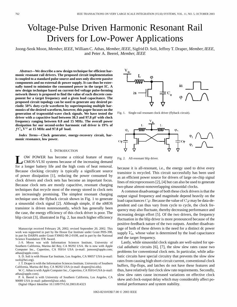
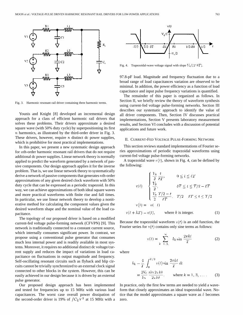
for a longer battery life and the high costs of heat removal.Because clocking circuitry is typically a significant sourceof power dissipation [1], reducing the power consumed byclock drivers and clock nets has become an important focus.Because clock nets are mostly capacitive, resonant chargingtechniques that recycle most of the energy stored in clock netsare increasingly promising. The simplest resonant chargingtechnique uses the flyback circuit shown in Fig. 1 to generatea sinusoidal clock signal [2]. Although simple, if the nMOStransistor is driven nonresonantly, which has generally beenthe case, the energy efficiency of this clock driver is poor. Theblip circuit [3], illustrated in Fig. 2, has much higher efficiency
Manuscript received February 28, 2002; revised September 20, 2002. Thiswork was supported in part by the House Ear Institute under Grant PHS-398,in part by DARPA under Grant F30602-98-2-0108, and in part by the NationalScience Foundation ITR Award.
J.-S. Moon was with Information Sciences Institute, University ofSouthern California, Marina del Rey, CA 90292 USA. He is now with AppleComputer Inc., Cupertino, CA 95014 USA (e-mail: [email protected];[email protected]).
S. D. Soli is with House Ear Institute, Los Angeles, CA 90057 USA (e-mail:[email protected]).
J. T. Draper is with the Information Sciences Institute, University of SouthernCalifornia, Marina del Rey, CA 90292 USA (e-mail: [email protected]).
W. C. Athas is with Apple Computer Inc., Cupertino, CA 95014 USA (e-mail:[email protected]).
P. A. Beerel is with University of Southern California, Los Angeles, CA90089 USA (e-mail: [email protected]).
Digital Object Identifier 10.1109/TVLSI.2003.814323
Fig. 1. Single-rail resonant clock driver (flyback circuit).
Fig. 2. All-resonant blip driver.
because it is all-resonant, i.e., the energy used to drive everytransistor is recycled. This circuit successfully has been usedas an efficient power source for drivers of large on-chip signallines of microprocessors [2], [4] but can also be used to generatetwo-phase almost-nonoverlapping sinusoidal clocks.
A common disadvantage of both these clock drivers is that theoutput signal frequency and magnitude depend heavily on theload capacitances . Because the value of may be data-de-pendent and can thus vary from cycle to cycle, the clock fre-quency may also fluctuate, thereby decreasing performance andincreasing design effort [5]. Of the two drivers, the frequencyfluctuation in the blip driver is more pronounced because of thepositive-feedback nature of the two outputs. Another disadvan-tage of both of these drivers is the need for a distinct dc powersupply whose value is determined by the load capacitanceand the target frequency.
Lastly, while sinusoidal clock signals are well-suited for spe-cial adiabatic circuits [6], [7], the slow slew rates cause twoproblems for conventional clock nets. In particular, while adia-batic circuits have special circuitry that prevents the slow slewrates from causing high short-circuit current, conventional clockbuffers, flip-flops, and latches do not have these features andthus, have relatively fast clock slew rate requirements. Secondly,slow slew rates cause increased variations on effective clockskew and clock-output delay which may considerably affect po-tential performance and system stability.
1063-8210/03$17.00 © 2003 IEEE
MOON et al.: VOLTAGE-PULSE DRIVEN HARMONIC RESONANT RAIL DRIVERS FOR LOW-POWER APPLICATIONS 763
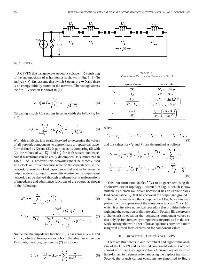
Fig. 3. Harmonic resonant rail driver containing three harmonic terms.
Younis and Knight [8] developed an incremental designapproach for a class of efficient harmonic rail drivers thatsolves these problems. Their drivers approximate a desiredsquare wave (with 50% duty cycle) by superpositioning its first
harmonics, as illustrated by the third-order driver in Fig. 3.These drivers, however, requiredistinct dc power supplies,which is prohibitive for most practical implementations.
In this paper, we present a new systematic design approachfor th-order harmonic resonant rail drivers that do not requireadditional dc power supplies. Linear network theory is normallyapplied to predict the waveform generated by a network of pas-sive components. Our design approach applies it for the inverseproblem. That is, we use linear network theory to systematicallyderive a network of passive components that generatesth-orderapproximations of any given desired clock waveform with 50%duty cycle that can be expressed as a periodic trapezoid. In thisway, we can achieve approximations of both ideal square wavesand more practical waveforms with finite rise and fall times.In particular, we use linear network theory to develop a nonit-erative method for calculating the component values given thedesired waveform shape and the nominal value of the load ca-pacitance.
The topology of our proposed driver is based on a modifiedcurrent-fed voltage pulse-forming network (CFVPN) [9]. Thisnetwork is traditionally connected to a constant current source,which internally consumes significant power. In contrast, wepropose using a conventional pulse generator that consumesmuch less internal power and is readily available in most sys-tems. Moreover, it requires no additional distinct dc voltage/cur-rent supply and reduces the impact of variations in load ca-pacitance on fluctuations in output magnitude and frequency.Self-oscillating resonant circuits such as flyback and blip cir-cuits cannot be trivially synchronized to an external clock signalconnected to other blocks in the system. However, this can beeasily achieved in our design because it is driven by an externalpulse generator.
Our proposed design approach has been implementedand tested for frequencies up to 15 MHz with various loadcapacitances. The worst case overall power dissipation ofthe second-order driver is 19% of at 15 MHz with a
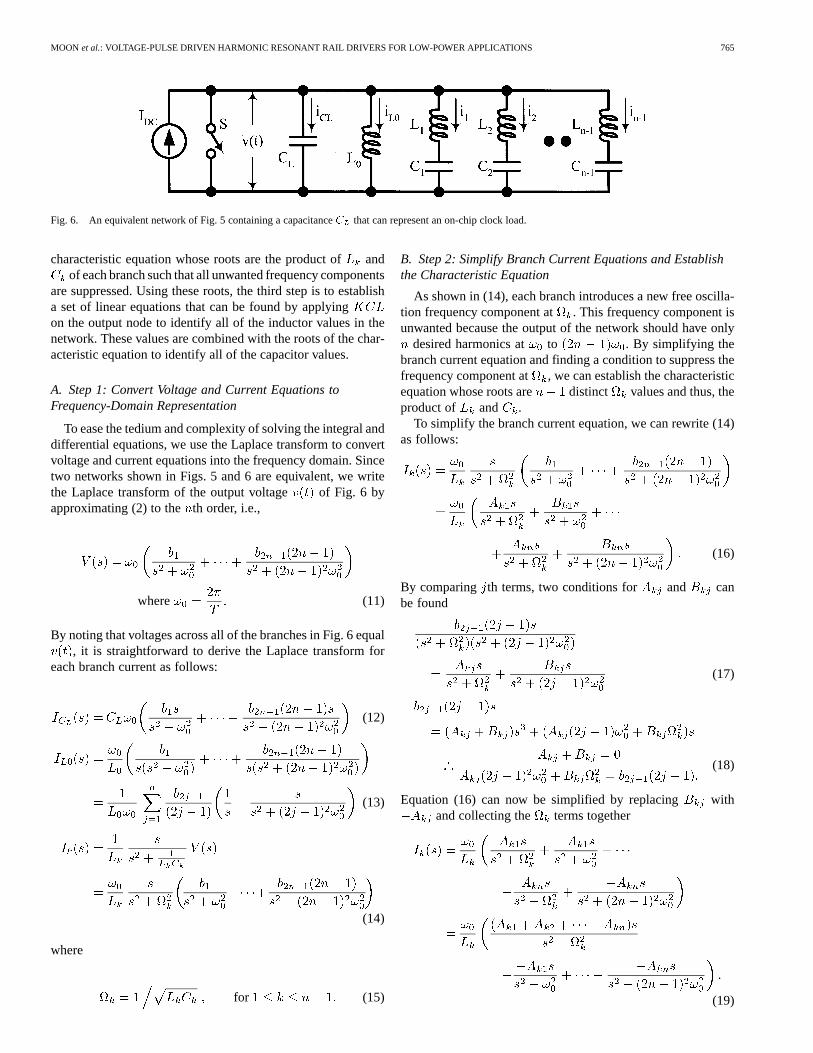
Fig. 4. Trapezoidal-wave voltage signal with slopeV =(2 �T ).
97.8-pF load. Magnitude and frequency fluctuation due to abroad range of load capacitances variation are observed to beminimal. In addition, the power efficiency as a function of loadcapacitance and input pulse frequency variations is quantified.
The remainder of this paper is organized as follows. InSection II, we briefly review the theory of waveform synthesisusing current-fed voltage pulse-forming networks. Section IIIdescribes our systematic approach to identify the value ofall driver components. Then, Section IV discusses practicalimplementations, Section V presents laboratory measurementresults, and Section VI concludes with a discussion of potentialapplications and future work.
II. CURRENT-FED VOLTAGE PULSE-FORMING NETWORK
This section reviews standard implementations of Fourier se-ries approximations of periodic trapezoidal waveforms usingcurrent-fed voltage pulse-forming networks.
A trapezoidal wave , shown in Fig. 4, can be defined bythe following:
where is integer. (1)
Because the trapezoidal waveform is an odd function, theFourier series for contains only sine terms as follows:
(2)
where
where (3)
In practice, only the first few terms are needed to yield a wave-form that closely approximates an ideal trapezoidal wave. No-tice that the model approximates a square wave asbecomeszero.
764 IEEE TRANSACTIONS ON VERY LARGE SCALE INTEGRATION (VLSI) SYSTEMS, VOL. 11, NO. 5, OCTOBER 2003
Fig. 5. CFVPN.
A CFVPN that can generate an output voltage consistingof the superposition of harmonics is shown in Fig. 5 [9]. Toanalyze , first assume that switch S opens at and thereis no energy initially stored in the network. The voltage acrossthe th section is shown in (4)
(4)
Cascading such sections in series yields the following for:
(5)
With this analysis, it is straightforward to determine the valuesof all network components to approximate a trapezoidal wave-form defined by (2) and (3). In particular, by comparing (5) with(2), the values of , , and for both square and trape-zoidal waveforms can be easily determined, as summarized inTable I. As is, however, this network cannot be directly usedas a clock rail driver because none of the capacitances in thenetwork represents a load capacitance that resides between theoutput node and ground. To meet this requirement, an equivalentnetwork can be derived through mathematical transformationsof impedance and admittance functions of the output, as shownin the following:
(6)
(7)
Notice that the impedance function has zeros at and, which in turn appear as poles in the admittance function
. We, therefore, can rewrite (7) as follows:
(8)
TABLE ICOMPONENTVALUES FORNETWORK OFFIG. 5
where
(9)and the values for and are determined as follows:
(10)
This transformation enables to be generated using thealternative circuit topology illustrated in Fig. 6, which is nowsuitable as a clock rail driver because it has an explicit clockload capacitance that lies between the output and ground.
To find the values of other components of Fig. 6, we can use apartial fraction expansion of the admittance function [10],which is an iterative numerical procedure that provides little in-sight into the operation of the network. In Section III, we presenta characteristic equation that constrains component values sothat only desired frequency components are produced in the net-work and together with a set of linear equations provides a moreinsightful closed-form expression for component values.
III. T HEORETICAL ANALYSIS OF CFVPN
There are three steps in our theoretical and algorithmic anal-ysis of the CFVPN and its desired component values. First, weconvert all of node voltage and branch current equations fromtime-domain to frequency-domain using the Laplace transform.Second, the branch current equations are simplified to find a
MOON et al.: VOLTAGE-PULSE DRIVEN HARMONIC RESONANT RAIL DRIVERS FOR LOW-POWER APPLICATIONS 765
Fig. 6. An equivalent network of Fig. 5 containing a capacitanceC that can represent an on-chip clock load.
characteristic equation whose roots are the product ofandof each branch such that all unwanted frequency components
are suppressed. Using these roots, the third step is to establisha set of linear equations that can be found by applyingon the output node to identify all of the inductor values in thenetwork. These values are combined with the roots of the char-acteristic equation to identify all of the capacitor values.
A. Step 1: Convert Voltage and Current Equations toFrequency-Domain Representation
To ease the tedium and complexity of solving the integral anddifferential equations, we use the Laplace transform to convertvoltage and current equations into the frequency domain. Sincetwo networks shown in Figs. 5 and 6 are equivalent, we writethe Laplace transform of the output voltage of Fig. 6 byapproximating (2) to the th order, i.e.,
where (11)
By noting that voltages across all of the branches in Fig. 6 equal, it is straightforward to derive the Laplace transform for
each branch current as follows:
(12)
(13)
(14)
where
for (15)
B. Step 2: Simplify Branch Current Equations and Establishthe Characteristic Equation
As shown in (14), each branch introduces a new free oscilla-tion frequency component at . This frequency component isunwanted because the output of the network should have only
desired harmonics at to . By simplifying thebranch current equation and finding a condition to suppress thefrequency component at , we can establish the characteristicequation whose roots are distinct values and thus, theproduct of and .
To simplify the branch current equation, we can rewrite (14)as follows:
(16)
By comparing th terms, two conditions for and canbe found
(17)
(18)
Equation (16) can now be simplified by replacing withand collecting the terms together
(19)
766 IEEE TRANSACTIONS ON VERY LARGE SCALE INTEGRATION (VLSI) SYSTEMS, VOL. 11, NO. 5, OCTOBER 2003
By applying on the output node of the network, the rela-tionship of branch currents can be defined by
(20)
Because no term exists in the right side of this equation, theterm in each branch current must evaluate to zero, implying
the following additional constraint
(21)
Equations (18) and (21) are combined to produce the character-istic equation shown in (23),
(22)
where (23)
Notice that the numerator of the characteristic equation is anorder-( ) polynomial of variable . The roots of this numer-ator polynomial, to , are the roots of the entire charac-teristic equation, which can be represented as follows:
(24)
C. Step 3: Setup Linear Equations to Find a Set ofandCombine With the Roots of the Characteristic Equation toFind a Set of
Using (24), we can substitute with the product andin (22) and use the result to simplify (20) as follows:
(25)
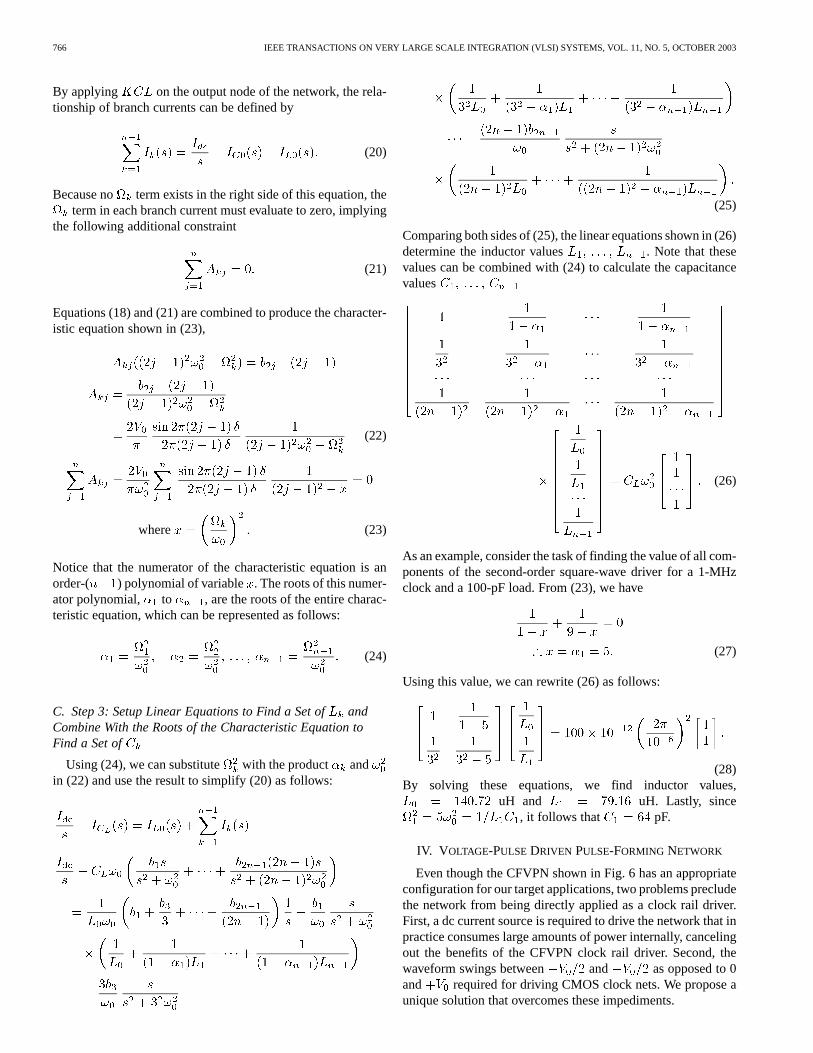
Comparing both sides of (25), the linear equations shown in (26)determine the inductor values . Note that thesevalues can be combined with (24) to calculate the capacitancevalues
(26)
As an example, consider the task of finding the value of all com-ponents of the second-order square-wave driver for a 1-MHzclock and a 100-pF load. From (23), we have
(27)
Using this value, we can rewrite (26) as follows:
(28)By solving these equations, we find inductor values,
uH and uH. Lastly, since, it follows that pF.
IV. V OLTAGE-PULSE DRIVEN PULSE-FORMING NETWORK
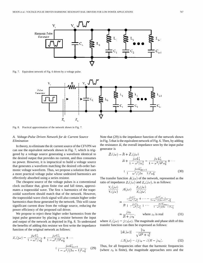
Even though the CFVPN shown in Fig. 6 has an appropriateconfiguration for our target applications, two problems precludethe network from being directly applied as a clock rail driver.First, a dc current source is required to drive the network that inpractice consumes large amounts of power internally, cancelingout the benefits of the CFVPN clock rail driver. Second, thewaveform swings between and as opposed to 0and required for driving CMOS clock nets. We propose aunique solution that overcomes these impediments.
MOON et al.: VOLTAGE-PULSE DRIVEN HARMONIC RESONANT RAIL DRIVERS FOR LOW-POWER APPLICATIONS 767
Fig. 7. Equivalent network of Fig. 6 driven by a voltage pulse.
Fig. 8. Practical approximation of the network shown in Fig. 7.
A. Voltage-Pulse Driven Network for dc Current SourceElimination
In theory, to eliminate the dc current source of the CFVPN wecan use the equivalent network shown in Fig. 7, which is trig-gered by a voltage source generating a waveform identical tothe desired output that provides no current, and thus consumesno power. However, it is impractical to build a voltage sourcethat generates a waveform matching the desiredth-order har-monic voltage waveform. Thus, we propose a solution that usesa more practical voltage pulse whose undesired harmonics areeffectively absorbed using a series resistor.
The cheapest source of the voltage pulses is a conventionalclock oscillator that, given finite rise and fall times, approxi-mates a trapezoidal wave. The firstharmonics of the trape-zoidal waveform should match that of the network. However,the trapezoidal-wave clock signal will also contain higher orderharmonics than those generated by the network. This will causesignificant current draw from the voltage source, reducing thepower efficiency of the proposed rail driver.
We propose to reject these higher order harmonics from theinput pulse generator by placing a resistor between the inputand output of the network as depicted in Fig. 8. To understandthe benefits of adding this resistor we first write the impedancefunction of the original network as follows:
(29)
Note that (29) is the impedance function of the network shownin Fig. 5 that is the equivalent network of Fig. 6. Then, by addingthe resistance , the overall impedance seen by the input pulsegenerator is
(30)
The transfer function of the network, represented as theratio of impedance and , is as follows:
where is real (31)
where . The magnitude and phase shift of thistransfer function can then be expressed as follows:
(32)
Thus, for all frequencies other than the harmonic frequencies(where is finite), the magnitude approaches zero and the
768 IEEE TRANSACTIONS ON VERY LARGE SCALE INTEGRATION (VLSI) SYSTEMS, VOL. 11, NO. 5, OCTOBER 2003
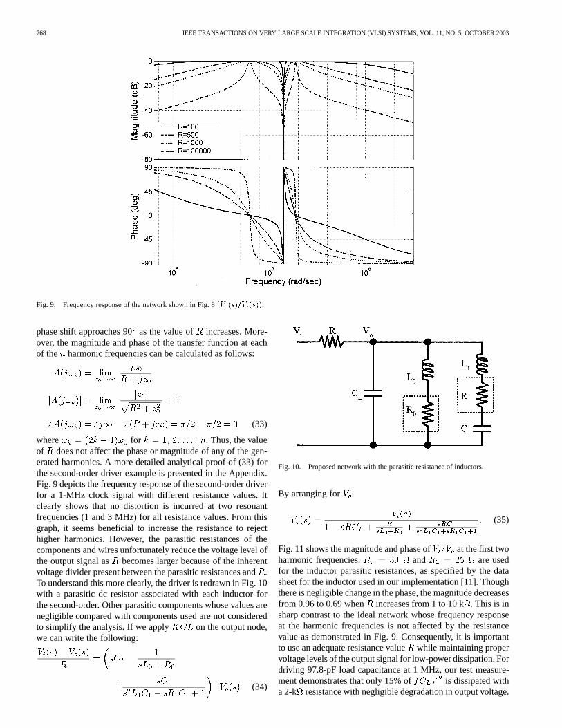
Fig. 9. Frequency response of the network shown in Fig. 8(V (s)=V (s)).
phase shift approaches 90as the value of increases. More-over, the magnitude and phase of the transfer function at eachof the harmonic frequencies can be calculated as follows:
(33)
where for . Thus, the valueof does not affect the phase or magnitude of any of the gen-erated harmonics. A more detailed analytical proof of (33) forthe second-order driver example is presented in the Appendix.Fig. 9 depicts the frequency response of the second-order driverfor a 1-MHz clock signal with different resistance values. Itclearly shows that no distortion is incurred at two resonantfrequencies (1 and 3 MHz) for all resistance values. From thisgraph, it seems beneficial to increase the resistance to rejecthigher harmonics. However, the parasitic resistances of thecomponents and wires unfortunately reduce the voltage level ofthe output signal as becomes larger because of the inherentvoltage divider present between the parasitic resistances and.To understand this more clearly, the driver is redrawn in Fig. 10with a parasitic dc resistor associated with each inductor forthe second-order. Other parasitic components whose values arenegligible compared with components used are not consideredto simplify the analysis. If we apply on the output node,we can write the following:
(34)
Fig. 10. Proposed network with the parasitic resistance of inductors.
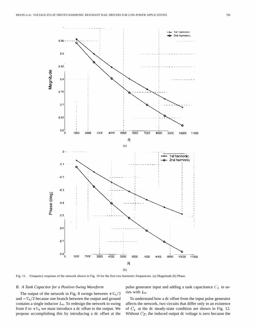
By arranging for
(35)
Fig. 11 shows the magnitude and phase of at the first twoharmonic frequencies. and are usedfor the inductor parasitic resistances, as specified by the datasheet for the inductor used in our implementation [11]. Thoughthere is negligible change in the phase, the magnitude decreasesfrom 0.96 to 0.69 when increases from 1 to 10 k. This is insharp contrast to the ideal network whose frequency responseat the harmonic frequencies is not affected by the resistancevalue as demonstrated in Fig. 9. Consequently, it is importantto use an adequate resistance valuewhile maintaining propervoltage levels of the output signal for low-power dissipation. Fordriving 97.8-pF load capacitance at 1 MHz, our test measure-ment demonstrates that only 15% of is dissipated witha 2-k resistance with negligible degradation in output voltage.
MOON et al.: VOLTAGE-PULSE DRIVEN HARMONIC RESONANT RAIL DRIVERS FOR LOW-POWER APPLICATIONS 769
(a)
(b)
Fig. 11. Frequency response of the network shown in Fig. 10 for the first two harmonic frequencies. (a) Magnitude (b) Phase.
B. A Tank Capacitor for a Positive-Swing Waveform
The output of the network in Fig. 8 swings betweenand because one branch between the output and groundcontains a single inductor . To redesign the network to swingfrom 0 to we must introduce a dc offset to the output. Wepropose accomplishing this by introducing a dc offset at the
pulse generator input and adding a tank capacitancein se-ries with .
To understand how a dc offset from the input pulse generatoraffects the network, two circuits that differ only in an existenceof at the dc steady-state condition are shown in Fig. 12.Without , the induced output dc voltage is zero because the

770 IEEE TRANSACTIONS ON VERY LARGE SCALE INTEGRATION (VLSI) SYSTEMS, VOL. 11, NO. 5, OCTOBER 2003
(a)
(b)
Fig. 12. dc steady-state for the network. (a) WithoutC . (b) WithC .
output and ground node are shorted by thebranch as shownin Fig. 12(a). As a result, the dc current flows intothe network, creating significant unwanted dc power. For thenetwork shown in Fig. 12(b), the tank capacitanceconnectedto in series induces a matching dc offset voltage at the outputnode, eliminating the dc current into the network.
Moreover, the introduction of the tank capacitor has a negli-gible impact on the overall frequency response of the rail driver.To see this, notice that the impedance functions for the branchesin Fig. 12 that contain can be written as follows:
(36)
Assuming is very large, the impedance of is negli-gibly affected by
when (37)
In our laboratory test, a 10 nF off-the-shelf capacitor was suf-ficient to achieve the desired dc offset voltage within an 0.8-to 15-MHz frequency range. The final proposed voltage-pulsedriven positive-swing driver is shown in Fig. 13.
V. MEASUREMENT
The proposed harmonic resonant square-wave rail driverscontaining up to four terms (i.e., fourth-order) were designedand tested on a wire-wrap board that included tunable inductorsand capacitors. We varied the frequency from 0.8 to 15 MHzby setting these components to theoretical values we calculatedusing (23) and (26). We then tuned each component to achieveminimum measured power dissipation and compared themwith their theoretical value. Testing at higher frequencies was
Fig. 13. Voltage-pulse driven harmonic resonant rail driver.
limited by the test setup and equipments that are available tothe authors.
Table II summarizes the laboratory measurement results forvarious configurations. In most cases, the measured values ofthe components are within 7% of the theoretical values. Devi-ation between the theoretical and tuned capacitance values islarger than for the inductors presumably because of the largeparasitic capacitances in our wire-wrapped board. As reportedin Table II, approximately 19% of the calculated conventionalpower dissipation was dissipated for the second-orderdriver at 15 MHz to drive 97.8 pF load capacitance. Power dissi-pation increases as the order of the driver increases. This effectappears to be due to more parasitic components in the test board.In addition, tuning the circuit for minimum measured power dis-sipation is increasingly error prone since more design variablesare involved. Note that as we increase the order of the driver, wemust include additional capacitance such asand for thesecond-order driver. However, this does not increase the powerdissipation significantly because only a small fraction of the cur-rent is drawn from the input pulse generator. In particular, thepulse generator needs to provide only a very small current suf-ficient to compensate the energy loss due to the parasitics of thecomponents.
The last row in Table II shows the measurement data of thesecond-order driver for different load capacitances at 1 MHz.Resistance values are reduced to achieve 10% rising and fallingtimes of the total cycle time. Power dissipation is increased byapproximately 7% for this case while rising and falling timesare shortened by 3% from the minimal power dissipation mode.This result suggests that by changing resistance value, we cancontrol the rising and falling times at the expense of power dis-sipation. Fig. 14 illustrates the measured power dissipation aswe changed the resistance valuefor 1 MHz and 100 pF. Thetransition time with 2-k resistance was measured as 110 ns,which is 11% of the total cycle time. Notice that transition timesin Fig. 14 are normalized to this value. At 285, the transitiontime drops to 50 ns (45%) while the power dissipation increasesfrom 15% to 57.9% of .
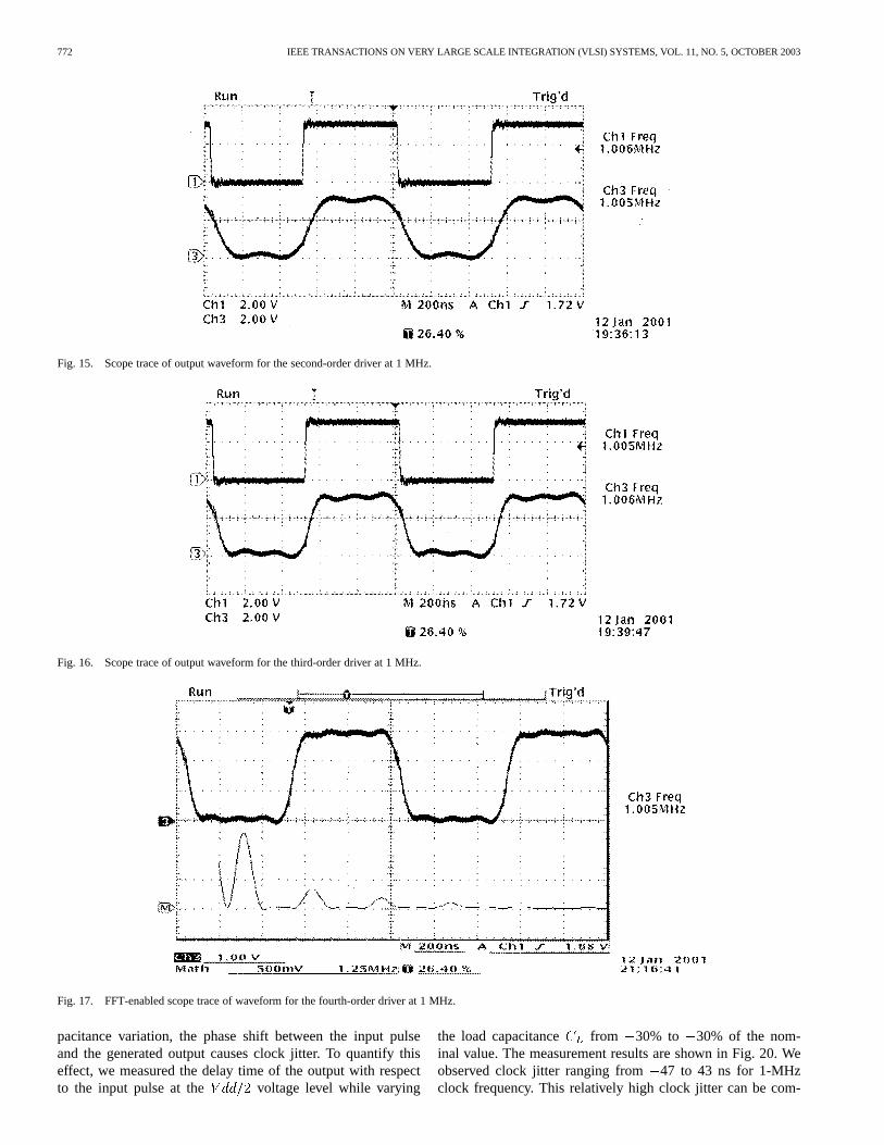
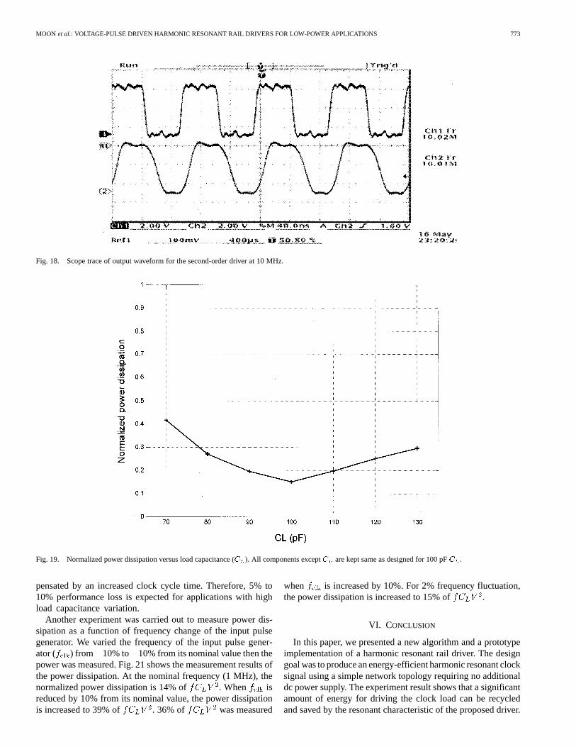
Figs. 15 and 16 show oscilloscope traces of the output signalof the driver for the second- and third-order harmonics. To seehow the output signal is synchronized, the input pulse is alsoshown. A fast Fourier (FFT)-enabled oscilloscope trace for thefourth-order driver output is presented in Fig. 17. The figureshows that only four harmonic frequencies are present in theoutput signal. Fig. 18 presents the trace of the output signal ofthe second-order harmonic driver for 10-MHz frequency.
When the driver is directly connected to the clock net-work, the nonlinear characteristic of the transistors can causeload capacitance variations. To measure power dissipation as

MOON et al.: VOLTAGE-PULSE DRIVEN HARMONIC RESONANT RAIL DRIVERS FOR LOW-POWER APPLICATIONS 771
TABLE IIMEASUREDDATA OF SECOND, THIRD, AND FOURTH SQUARE-WAVE HARMONIC RESONANT RAIL DRIVER FORVARIOUS CLOCK FREQUENCIES ANDLOAD
CAPACITANCES. THE FIRST THREEROWS AREDATA FOR DRIVING 97.8 pF LOAD CAPACITANCE AT DIFFERENTCLOCK FREQUENCIES AND THELAST ROW SHOWS
DATA FOR DIFFERENTLOAD CAPACITANCES AT 1 MHz. THEORETICAL AND MEASUREDVALUES OFEACH COMPONENT AREALSO SHOWN FORCOMPARISON
Fig. 14. Normalized power dissipation(P=fC V ) and transition time versus resistanceR. fC V is the theoretical conventional power dissipation to driveload capacitanceC .
a function of the load capacitance variation, we variedfrom 30% to 30% of the nominal value while keeping allother components the same. The power was then measured.The results for a 1-MHz clock and a 100-pF load capacitanceare plotted in Fig. 19. Normalized power dissipation in thegraph is the ratio between the measured power dissipationand . Power dissipation at 100 pF is minimum be-cause the circuit is designed to harmonically resonate at thisvalue. No frequency variation was noticed for this range ofcapacitances as is expected for any externally-driven driver.
Unlike the self-oscillating rail drivers whose frequency variesproportional to the square root of variations in capacitance[5], this beneficial characteristic of our drivers significantlyincreases system stability. For capacitance greater than 130%,however, significant voltage-level degradation is observed. Onthe other hand, if we reduce the load capacitance below 70%of nominal, the power dissipation increases rapidly becausecurrent from the input pulse generator mostly charges theload capacitance instead of it being charged resonantly. Inaddition to the increased power dissipation by the load ca-
772 IEEE TRANSACTIONS ON VERY LARGE SCALE INTEGRATION (VLSI) SYSTEMS, VOL. 11, NO. 5, OCTOBER 2003
Fig. 15. Scope trace of output waveform for the second-order driver at 1 MHz.
Fig. 16. Scope trace of output waveform for the third-order driver at 1 MHz.
Fig. 17. FFT-enabled scope trace of waveform for the fourth-order driver at 1 MHz.
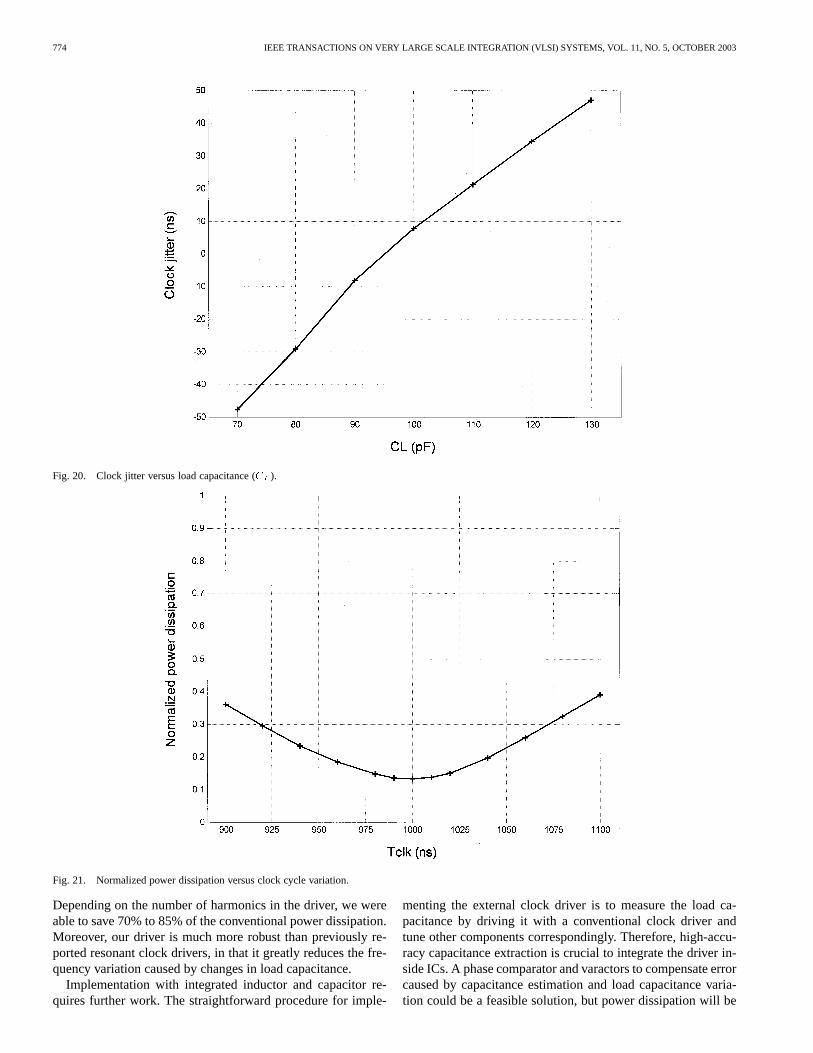
pacitance variation, the phase shift between the input pulseand the generated output causes clock jitter. To quantify thiseffect, we measured the delay time of the output with respectto the input pulse at the voltage level while varying
the load capacitance from 30% to 30% of the nom-inal value. The measurement results are shown in Fig. 20. Weobserved clock jitter ranging from 47 to 43 ns for 1-MHzclock frequency. This relatively high clock jitter can be com-
MOON et al.: VOLTAGE-PULSE DRIVEN HARMONIC RESONANT RAIL DRIVERS FOR LOW-POWER APPLICATIONS 773
Fig. 18. Scope trace of output waveform for the second-order driver at 10 MHz.
Fig. 19. Normalized power dissipation versus load capacitance (C ). All components exceptC are kept same as designed for 100 pFC .
pensated by an increased clock cycle time. Therefore, 5% to10% performance loss is expected for applications with highload capacitance variation.
Another experiment was carried out to measure power dis-sipation as a function of frequency change of the input pulsegenerator. We varied the frequency of the input pulse gener-ator ( ) from 10% to 10% from its nominal value then thepower was measured. Fig. 21 shows the measurement results ofthe power dissipation. At the nominal frequency (1 MHz), thenormalized power dissipation is 14% of . When isreduced by 10% from its nominal value, the power dissipationis increased to 39% of . 36% of was measured
when is increased by 10%. For 2% frequency fluctuation,the power dissipation is increased to 15% of .
VI. CONCLUSION
In this paper, we presented a new algorithm and a prototypeimplementation of a harmonic resonant rail driver. The designgoal was to produce an energy-efficient harmonic resonant clocksignal using a simple network topology requiring no additionaldc power supply. The experiment result shows that a significantamount of energy for driving the clock load can be recycledand saved by the resonant characteristic of the proposed driver.
774 IEEE TRANSACTIONS ON VERY LARGE SCALE INTEGRATION (VLSI) SYSTEMS, VOL. 11, NO. 5, OCTOBER 2003
Fig. 20. Clock jitter versus load capacitance (C ).
Fig. 21. Normalized power dissipation versus clock cycle variation.
Depending on the number of harmonics in the driver, we wereable to save 70% to 85% of the conventional power dissipation.Moreover, our driver is much more robust than previously re-ported resonant clock drivers, in that it greatly reduces the fre-quency variation caused by changes in load capacitance.
Implementation with integrated inductor and capacitor re-quires further work. The straightforward procedure for imple-
menting the external clock driver is to measure the load ca-pacitance by driving it with a conventional clock driver andtune other components correspondingly. Therefore, high-accu-racy capacitance extraction is crucial to integrate the driver in-side ICs. A phase comparator and varactors to compensate errorcaused by capacitance estimation and load capacitance varia-tion could be a feasible solution, but power dissipation will be

MOON et al.: VOLTAGE-PULSE DRIVEN HARMONIC RESONANT RAIL DRIVERS FOR LOW-POWER APPLICATIONS 775
Fig. 22. Waveform plot forv (t) in (46).
increased by these additional circuitries. In addition, the low-Qcharacteristic of the internal inductor may cause low power ef-ficiency of the harmonic clock driver.
For high-frequency applications, the parasitic componentsof each inductor and capacitor will significantly affect theoutput waveform and power dissipation. Therefore, a simula-tion-based optimization strategy is needed to achieve optimumperformance and power dissipation. Nevertheless, the theo-retically-optimal circuit derived from our analysis can be theinitial circuit for a more detailed nonlinear simulation-basedoptimization strategy. Providing such a good initial conditioncan dramatically reduce the run time of the simulation-basedapproach. In addition, the theoretic analysis may also be usefulin guiding the search strategy.
APPENDIX
PROOF OF(33) FOR THESECOND-ORDER DRIVER
By applying on the output node of Fig. 8 (for thesecond-order driver), we can write the following:
(38)
can be rewritten as shown in (39) at the bottom of the page.For the second-order square-wave driver, all of the componentscan be represented with and as follows:
(40)
Using (40), we can simplify (39) into (41)
(41)To show how input harmonic signals are not affected bythe series resistor , let us examine the output when sinewave is applied. Note that idealsquare-wave is the sum of the sine waves harmonically related
(39)

776 IEEE TRANSACTIONS ON VERY LARGE SCALE INTEGRATION (VLSI) SYSTEMS, VOL. 11, NO. 5, OCTOBER 2003
( ). Using partial fraction expansion, the followingcan be established
(42)
By comparing (41) and (42), we find
(43)
Solving for and
(44)
Notice that when and 3, is forced to zero which in turnsimplifies other terms as shown below
(45)
Therefore, for or 3, (42) becomes
(46)
From this equation, we can conclude the first two harmonicsfrom the input pulse generator are not affected by the series re-sistor and thus appear at the output node with the same mag-nitude and phase. Fig. 22 shows the time-domain waveform of
for various values. As shown in the figure, the magni-tude of always converges to zero regardless ofvalue.
Therefore, when the circuit reaches steady-state condition, onlythe first two harmonics are present at the output node and nopower is dissipated if the input is composed of these two har-monics.
REFERENCES
[1] J. Rabaey, Digital Integrated Circuits: A Design Perspec-tive. Englewood Cliffs, NJ: Prentice-Hall, 1995.
[2] W. Athas, N. Tzartzanis, L. Svensson, and L. Peterson, “A low-powermicroprocessor based on resonant energy,”IEEE J. Solid-State Circuits,vol. 32, pp. 1693–1701, Nov. 1997.
[3] W. Athas, L. Svensson, and N. Tzartzanis, “A resonant signal driver fortwo-phase, almost-nonoverlapping clocks,” inProc. Int. Symp. Circuitsand Systems, 1996, pp. 129–132.
[4] W. Athas, N. Tzartzanis, W. Mao, L. Peterson, R. Lal, K. Chong, J.-S.Moon, L. Svensson, and M. Bolotski, “The design and implementa-tion of a low-power clock-powered microprocessor,”IEEE J. Solid-StateCircuits, vol. 35, pp. 1561–1570, Nov. 2000.
[5] N. Tzartzanis, “Energy-recovery technique for CMOS microprocessordesign,” Ph.D. dissertation, Dept. Elect. Eng., Univ. of Southern Cali-fornia, Los Angeles, CA, 1998.
[6] W. Athas, L. Svensson, J. Koller, N. Tzartzanis, and Y. Chou, “Low-power digital systems based on adiabatic-switching principles,”IEEETrans. VLSI Syst., vol. 2, pp. 398–406, Dec. 1994.
[7] J. Denker, “A review of adiabatic computing,” inProc. 1994 Symp. Low-Power Electronics, 1994, pp. 94–97.
[8] S. Younis and T. Knight, “Non-dissipative rail drivers for adiabatic cir-cuits,” inProc. 16th Conf. Advanced Research VLSI, 1995, pp. 404–414.
[9] G. Glasoe and J. Lebacqz, Eds.,Pulse Generator. New York: Mc-Graw-Hill, 1948, pp. 175–224.
[10] M. Van Valkenburg,Network Analysis. Englewood Cliffs, NJ: Pren-tice-Hall, 1974.
[11] Coilcraft Document 112-1, Slot Seven 7mm Tunable Inductor DataSheet. Cary, IL: Coilcraft, Inc., 2001.
Joong-Seok Moon(S’97–M’03) received the B.S.E.E. and M.S.E.E. degreesfrom the Seoul National University, Korea, in 1993 and 1995, respectively, andthe Ph.D. degree in electrical engineering from the University of Southern Cal-ifornia, Los Angeles, in 2003.
Currently, he is a VLSI Application Engineering with Apple Computer, Inc,Cupertino, CA. From 1995 to 1996, he was a VLSI Engineer with SamsungElectronics, Korea. He was also with Information Sciences Institutes, Universityof Southern California, Marina del Rey, CA where he was involved in severalVLSI research projects such as low–power microprocessor, feedback cancel-lation DSP chip for hearing-aid, low-power FIFO SRAM, and floating–pointunit for DIVA processor-in-memory processor. His research interests includeare low-power circuit and system design for general purpose and DSP architec-ture.
William C. Athas (M’99) received the B.S. degree in computer science fromthe University of Utah, Salt Lake City, in 1978, and the Ph.D. degree from theCalifornia Institute of Technology, Pasadena, CA, in 1987.
In 2000, he joined Apple Computer, Inc., Cupertino, CA, where he is a VLSISystems Architect and Principal Engineer in the VLSI-Hardware EngineeringDepartment. At Apple he works in the areas of high-speeding signaling, mixed-signal integrated-circuit designs, microprocessor speed and power modeling,and advanced microarchitecture concepts and designs. From 1991 to 2000, hewas a Research Scientist and Senior Project Leader with the Information Sci-ences Institute, University of Southern California, Marina del Rey, CA. Duringthis time he was the Team Leader for the design and implementation of the AC1microprocessor, which demonstrated a new approach to low-power computingbased on the principle of energy recovery. He has 23 publications in the areasof the theory and design of low-power circuits and high-performance computerarchitecture. He has received patents for low-power and asynchronous circuits,high-performance memory subsystems, and network hardware.
Sigfrid D. Soli photograph and biography not available at the time of publica-tion.
MOON et al.: VOLTAGE-PULSE DRIVEN HARMONIC RESONANT RAIL DRIVERS FOR LOW-POWER APPLICATIONS 777
Jeffrey T. Draper (S’85–M’89) received the B.S. degree in electrical engi-neering from Texas A&M University, College Station, TX, in 1987, and theM.S.E. and Ph.D. degrees in electrical engineering from University of Texas,Austin, TX, in 1990 and 1993, respectively.
He is a Research Assistant Professor at the University of Southern California(USC), Los Angeles, and is also a Project Leader with the Information SciencesInstitute, USC, where he has been working in research since 1993. He has ledthe VLSI effort on several DARPA-funded projects and has produced a numberof complex ICs, with the most recent chip fabricated in 0.18�m technology andcontaining 55 million transistors.
Peter A. Beerel (S’88–M’95) received the B.S.E. degree in electrical engi-neering from Princeton University, Princeton, NJ, in 1989, and the M.S. andPh.D. degrees in electrical engineering from Stanford University, Stanford, CA,in 1991 and 1994, respectively.
Currently, he is the Vice-President of Asynchronous Computer-Aided Designand Verification at Fulcrum Microsystems, Inc., Calabasas Hills, CA, a startupcompany developing and commercializing asynchronous designs. He is also anAssociate Professor, currently on leave, from the Department of Electrical Engi-neering-Systems at the University of Southern California (USC), Los Angeles.He has consulted for Yuni Networks and AMCC in the areas of networking chipdesign, Intel, and asynchronous digital design in the areas of asynchronous de-sign and computer-aided design, and TrellisWare Technologies in the area ofcommunication chip design. His research interests include a variety of topics inCAD and VLSI.
Dr. Beerel received the Outstanding Teaching Award in 1997 and the JuniorResearch Award in 1998, from the School of Engineering, USC. He received aNational Science Foundation (NSF) Career Award and a 1995 Zumberge Fel-lowship. He was also co-recipient of the Charles E. Molnar Award for two paperspublished in ASYNC’97 that best bridged theory and practice of asynchronoussystem design and was a co-recipient of the best paper award in ASYNC’99.He is coauthor of four patents in the area of asynchronous circuits. He has beena Member of the Technical Program Committee for the International Sympo-sium on Advanced Research in Asynchronous Circuits and Systems since 1997and was Program Co-chair for ASYNC’98. He has served on the Technical Pro-gram Committee for the International Conference on Computer-Aided Designin 2000 and 2001.