aprototype processing-in-memory (pim) chip for the …draper/papers/jvlsi_05.pdfjournal of vlsi...
TRANSCRIPT

Journal of VLSI Signal Processing 40, 73–84, 2005c© 2005 Springer Science + Business Media, Inc. Manufactured in The Netherlands.
A Prototype Processing-In-Memory (PIM) Chip for the Data-IntensiveArchitecture (DIVA) System
JEFFREY DRAPER, J. TIM BARRETT, JEFF SONDEEN, SUMIT MEDIRATTA,CHANG WOO KANG, IHN KIM AND GOKHAN DAGLIKOCA
University of Southern California, Information Sciences Institute, 4676 Admiralty Way,Marina del Rey, CA 90292, USA
Received November 15, 2002; Revised November 11, 2003; Accepted November 13, 2003
Abstract. The Data-Intensive Architecture (DIVA) system employs Processing-In-Memory (PIM) chips as smart-memory coprocessors. This architecture exploits inherent memory bandwidth both on chip and across the system totarget several classes of bandwidth-limited applications, including multimedia applications and pointer-based andsparse-matrix computations. The DIVA project has built a prototype development system using PIM chips in placeof standard DRAMs to demonstrate these concepts. We have recently ported several demonstration kernels to thisplatform and have exhibited a speedup of 35X on a matrix transpose operation.
This paper focuses on the 32-bit scalar and 256-bit WideWord integer processing components of the first DIVAprototype PIM chip, which was fabricated in TSMC 0.18 µm technology. In conjunction with other publications, thispaper demonstrates that impressive gains can be achieved with very little “smart” logic added to memory devices.A second PIM prototype that includes WideWord floating-point capability is scheduled to tape out in August 2003.
Keywords: processing-in-memory, memory wall, memory bandwidth
1. Introduction
The increasing gap between processor and memoryspeeds is a well-known problem in computer archi-tecture, with peak processor performance increasing ata rate of 50–60% per year while memory access timesimprove at merely 5–7%. Furthermore, techniques de-signed to hide memory latency, such as multithreadingand prefetching, actually increase the memory band-width requirements [1]. A recent VLSI technologytrend, embedded DRAM, offers a promising solutionto bridging the processor-memory gap [2]. One appli-cation of this technology integrates logic with high-density memory in a processing-in-memory (PIM)chip. Because PIM internal processors can be directlyconnected to the memory banks, the memory band-width is dramatically increased (with hundreds of giga-bit/second aggregate bandwidth available on a chip—
up to 2 orders of magnitude over conventional DRAMsystems). Latency to on-chip logic is also reduced,down to as little as one half that of a conventional mem-ory system, because internal memory accesses avoidthe delays associated with communicating off chip.
The Data-Intensive Architecture (DIVA) project em-ploys PIM technology in “smart memory” devices thatare capable of very large amounts of processing. Thesedevices are used to replace or augment the memorysystem of a conventional workstation. System band-width limitations are overcome in three ways: (1) tightcoupling of a single PIM processor with an on-chipmemory bank through a wide datapath; (2) replica-tion of processor-memory nodes throughout the sys-tem; and, (3) utilizing a separate chip-to-chip intercon-nect that allows PIM chips to communicate withoutinterfering with host memory bus traffic. Although suit-able as a general-purpose computing platform, DIVA
74 Draper et al.
specifically targets two important classes of applica-tions that are severely performance limited by theprocessor-memory bottlenecks in conventional sys-tems: multimedia processing and applications with ir-regular data accesses. Multimedia applications tend tohave little temporal reuse [3] but often exhibit spatial lo-cality and both fine-grain and coarse-grain parallelism.DIVA PIMs exploit spatial locality and fine-grain paral-lelism by accessing and operating upon multiple wordsof data at a time and exploit coarse-grain parallelismby spreading independent computations across PIMnodes. Applications with irregular data accesses, suchas sparse-matrix and pointer-based computations, per-form poorly on conventional architectures because theytend to lack spatial locality and thus make poor use ofcaches. As a result, their execution is dominated bymemory stalls [4]. DIVA accelerates such applicationsby eliminating much of the traffic between a host pro-cessor and memory; simple operations and dereferenc-ing can be done mostly within PIM memories.
This paper focuses on the microarchitecture designof the DIVA PIM processing components, consistingprimarily of a 32-bit scalar processor and 256-bit Wide-Word Unit. Due to area constraints, the design goal wasa relatively simple processor with a coherent, well-designed instruction set, for which a gcc-like com-piler is being adapted. The resulting processor sup-ports single-issue, in-order execution, with 32-bit in-structions and 32-bit addresses. Its novelty lies in thespecial-purpose functions it supports and the tight in-tegration of the scalar and WideWord datapaths. Thispaper also highlights details of the prototype DIVAPIM chip and development system implementation.The prototype chip was fabricated in TSMC 0.18 µmtechnology, and the development system employing in-stances of this chip has demonstrated a speedup of 35xon a matrix transpose operation. Other computationkernels have been ported to this system, and instru-mented measurements are currently being performed.The remainder of the paper is organized as follows.Sections 2 and 3 present an overview of the DIVAsystem architecture and chip organization, to put theprocessor design into its proper context. Section 4 de-scribes the PIM processor microarchitecture in detail,including scalar and WideWord datapaths. Section 5presents details of the fabrication, testing, and systemintegration of the prototype PIM chip. Descriptions ofhow the DIVA concept differs from related work aregiven in Section 6, and Section 7 concludes the paperand briefly describes ongoing and future work.
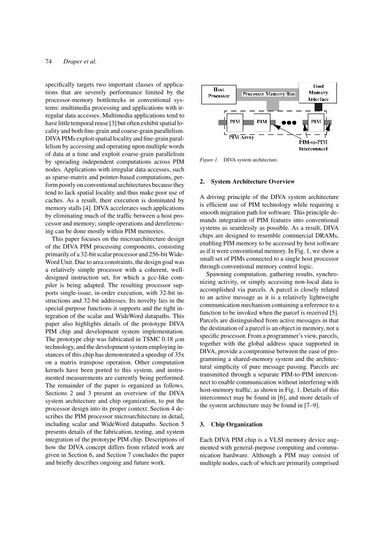
Figure 1. DIVA system architecture.
2. System Architecture Overview
A driving principle of the DIVA system architectureis efficient use of PIM technology while requiring asmooth migration path for software. This principle de-mands integration of PIM features into conventionalsystems as seamlessly as possible. As a result, DIVAchips are designed to resemble commercial DRAMs,enabling PIM memory to be accessed by host softwareas if it were conventional memory. In Fig. 1, we show asmall set of PIMs connected to a single host processorthrough conventional memory control logic.
Spawning computation, gathering results, synchro-nizing activity, or simply accessing non-local data isaccomplished via parcels. A parcel is closely relatedto an active message as it is a relatively lightweightcommunication mechanism containing a reference to afunction to be invoked when the parcel is received [5].Parcels are distinguished from active messages in thatthe destination of a parcel is an object in memory, not aspecific processor. From a programmer’s view, parcels,together with the global address space supported inDIVA, provide a compromise between the ease of pro-gramming a shared-memory system and the architec-tural simplicity of pure message passing. Parcels aretransmitted through a separate PIM-to-PIM intercon-nect to enable communication without interfering withhost-memory traffic, as shown in Fig. 1. Details of thisinterconnect may be found in [6], and more details ofthe system architecture may be found in [7–9].
3. Chip Organization
Each DIVA PIM chip is a VLSI memory device aug-mented with general-purpose computing and commu-nication hardware. Although a PIM may consist ofmultiple nodes, each of which are primarily comprised

Prototype Processing-In-Memory (PIM) Chip 75
Figure 2. DIVA PIM chip architecture.
of a few megabytes of memory and a node processor,Fig. 2 shows a PIM with a single node, which reflectsthe focus of the initial research that is being conducted.Nodes on a PIM chip share a single PIM Routing Com-ponent (PiRC) and a host interface. The PiRC is respon-sible for routing parcels between on-chip parcel buffersand neighboring off-chip PiRCs. The host interface im-plements the JEDEC standard SDRAM protocol [10]so that memory accesses as well as parcel activity ini-tiated by the host appear as conventional memory ac-cesses from the host perspective.
Figure 2 also shows two interconnects that span aPIM chip for information flow between nodes, the hostinterface, and the PiRC. Each interconnect is distin-guished by the type of information it carries. The PIMmemory bus is used for conventional memory accessesfrom the host processor. The parcel interconnect allowsparcels to transit between the host interface, the nodes,and the PiRC. Within the host interface, a parcel buffer(PBUF) is a buffer that is memory-mapped into thehost processor’s address space, permitting application-level communication through parcels. Each PIM nodealso has a PBUF, memory-mapped into the node’s localaddress space.
Figure 3 shows the major control and data connec-tions within a node. The DIVA PIM node processinglogic supports single-issue, in-order execution, with32-bit instructions and 32-bit addresses. There are twodatapaths whose actions are coordinated by a single ex-ecution control unit: a 32-bit scalar datapath that per-forms operations similar to those of standard 32-bitinteger units, and a 256-bit WideWord datapath thatperforms fine-grain parallel operations on 8-, 16-, or32-bit operands. Both datapaths execute from a singleinstruction stream under the control of a single 5-stage
Figure 3. DIVA PIM node organization.
DLX-like pipeline [11]. This pipeline fetches instruc-tions from a small instruction cache, which is includedto minimize memory contention between instructionreads and data accesses. The instruction set has beendesigned so both datapaths can, for the most part, usethe same opcodes and condition codes, generating alarge functional overlap. Each datapath has its own in-dependent general-purpose register file, 32 32-bit regis-ters for the scalar datapath and 32 256-bit registers forthe WideWord datapath, but special instructions per-mit direct transfers between datapaths without goingthrough memory. Although not supported in the ini-tial DIVA prototype, floating-point extensions to theWideWord unit will be provided in future systems.
4. Microarchitecture Detailsof the DIVA Processor
The combination of the execution control unit andscalar datapath is for the most part a standard RISCprocessor and serves as the DIVA scalar processor,or microcontroller. It coordinates all activity within aDIVA PIM node, including SIMD-like operations inthe WideWord datapath, interactions between the scalarand WideWord datapaths, and parcel communication.To avoid synchronization overhead and compiler is-sues associated with coprocessor designs and also de-sign complexity associated with superscalar interlocks,the DIVA processor was designed with a tight inte-gration between the scalar and WideWord datapaths.The following sections describe the execution pipeline,

76 Draper et al.
scalar datapath, WideWord datapath, and interactionsbetween the scalar and WideWord datapaths. The de-scription of the execution pipeline is encapsulated withthe scalar datapath, since this combination serves as acore PIM node controller.
4.1. Details of the Execution Pipelineand Scalar Datapath
The tight integration between the scalar datapath andother components, most notably the WideWord datap-ath, led to a custom design rather than augmenting anoff-the-shelf embedded IP core. This section describesthe microarchitecture of the DIVA scalar processor byfirst presenting an overview of the instruction set archi-tecture, followed by a description of the pipeline anddiscussion of special features.
4.1.1. Instruction Set Architecture Overview. Muchlike the DLX architecture [11], most DIVA scalar in-structions use a three-operand format to specify twosource registers and a destination register, as shown inFig. 4. For these types of instructions, the opcode gen-erally denotes a class of operations, such as arithmetic,and the function denotes a specific operation, such asadd. The C bit indicates whether the operation per-formed by the instruction execution updates conditioncodes. In lieu of a second source register, a 16-bit im-mediate value may be specified. The scalar instructionset includes the typical arithmetic functions add, sub-tract, multiply, and divide; logical functions AND, OR,NOT, and XOR; and logical/arithmetic shift operations.In addition, there are a number of special instructions,
Figure 4. DIVA scalar arithmetic/logical instruction formats.
Figure 5. DIVA branch instruction formats.
described in Section 4.1.3. Load/store instructions ad-here to the immediate format, where the address forthe memory operation is formed by the addition of animmediate value to the contents of rA, which servesas a base address. The DIVA scalar processor does notsupport a base-plus-register addressing mode becausesupporting such a mode for store operations requireseither an extra read port on the register file or pipelinestalls to allow multiple register file reads for a singlestore instruction.
Branch instructions use a different instruction for-mat, as shown in Fig. 5. The branch target address maybe PC-relative, useful for relocatable code, or calcu-lated using a base register combined with an offset,useful with table-based branch targets. In both formats,the offset is in units of instruction words, or 4 bytes.By specifying the offset in instruction words, ratherthan bytes, a larger branch window results. To supportfunction calls, the branch instruction format includesan L bit for specifying linkage, that is, whether a returninstruction address should be saved in R31. The branchformat also includes a 3-bit condition field, CCC, tospecify one of eight branch conditions: always, equal,not equal, less than, less than or equal, greater than,greater than or equal, or overflow.
4.1.2. Pipeline Description and Associated Hazards.A depiction of the pipeline execution control unit andscalar datapath are given in Fig. 6. The pipeline is astandard DLX-like 5-stage pipeline [11], with the fol-lowing stages: (1) instruction fetch; (2) decode and reg-ister read; (3) execute; (4) memory; and, (5) writeback.The pipeline controller contains the necessary logicto handle data, control, and structural hazards. Data

Prototype Processing-In-Memory (PIM) Chip 77
Figure 6. DIVA scalar processor pipeline description.
hazards occur when there are read-after-write registerdependences between instructions that co-exist in thepipeline. The controller and datapath contain the nec-essary forwarding, or bypass, logic to allow pipelineexecution to proceed without stalling in most data de-pendence cases. The only exception to this generalityinvolves the load instruction, where a “bubble” is in-serted between the load instruction and an immediatelyfollowing instruction that uses the load target register asone of its source operands. This hazard is handled withhardware interlocks, rather than exposing it to soft-ware, to be compatible with a previously developedcompiler.
Control hazards occur for branch instructions. Un-like the DLX architecture [11], which uses explicitcomparison instructions and testing of a general-purpose register value for branching decisions, theDIVA design incorporates condition codes that maybe updated by most instructions. Although a slightlymore complex design, this scheme obviates the needfor several comparison instructions in the instructionset and also requires one fewer instruction executionin every comparison/branch sequence. The conditioncodes used for branching decisions are: EQ—set if theresult is zero, LT—set if the result is negative, GT—set if the result is positive, and OV—set if the opera-tion overflows. Unlike the load data dependence haz-ard, which is not exposed to the compiler, the DIVApipeline design imposes a 1-delay slot branch, so thatthe instruction following a branch instruction is alwaysexecuted. Since branches are always resolved withinthe second stage of the pipeline, no stalls occur withbranch instructions. The delayed branch was selected
because it was compatible with a previously developedcompiler.
Since the general-purpose register file contains 2read ports and 1 write port, it may sustain two operandreads and 1 result write every clock cycle; thus, theregister file design introduces no structural hazards.The only structural hazard that impacts the pipelineoperation is the node memory. Pipeline stalls occurwhen there is an instruction cache miss. The pipelinewill resume once the cache fill memory request hasbeen satisfied. Likewise, since there is no data cache,stalls occur any time a load/store instruction reachesthe memory stage of the pipeline until the memoryoperation is completed.
4.1.3. Special Features. The novelty of the DIVAscalar processor lies in the special features that sup-port DIVA-specific functions. Although by no meansexhaustive, this section highlights some of the morenotable capabilities. Additional features concerning theinteraction between the scalar processor and WideWorddatapath are described in Section 4.3.
Run-Time Kernel Support. The execution control unitsupports supervisor and user modes of processing andalso maintains a number of special-purpose and pro-tected registers for support of exception handling, ad-dress translation, and general OS services. Exceptions,arising from execution of node instructions, and inter-rupts, from other sources such as an internal timer or ex-ternal component like the PBUF, are handled by a com-mon mechanism. The exception handling scheme forDIVA has a modest hardware requirement, exporting
78 Draper et al.
much of the complexity to software, to maintain a flex-ible implementation platform. It provides an integratedmechanism for handling hardware and software excep-tion sources and a flexible priority assignment schemethat minimizes the amount of time that exception recog-nition is disabled. While the hardware design allowstraditional stack-based exception handlers, it also sup-ports a dispatching scheme that uses DIVA hardwarefeatures to allow preemption of lower-priority excep-tion handlers.
The impact of run-time kernel support on the scalarprocessor design is the addition of a modest numberof special-purpose and protected (or supervisor-level)registers and a non-negligible amount of complexityadded to the pipeline control for entering/exiting ex-ception handling modes cleanly. When an exception isdetected by the scalar processor control unit, the logicperforms a number of tasks within a single clock cy-cle to prepare the processor for entering an exceptionhandler in the next clock cycle. Those tasks include:
• determining which exception to handle by prioritiz-ing among simultaneously occurring exceptions,
• setting up shadow registers to capture critical state in-formation, such as the processor status word register,the instruction address of the faulting instruction, thememory address if the exception is an address fault,etc,
• configuring the program counter logic to load an ex-ception handler address on the next clock cycle, and
• setting up the processor status word register to entersupervisor mode with exception handling temporar-ily disabled.
Once invoked, the exception handler first stores otherpieces of user state and interrogates various piecesof state hardware to determine how to proceed. De-pending on the exception type, the handler may re-enable some higher-priority exceptions at this point.Once the exception handler routine has completed, itrestores user state and then executes a return-from-exception instruction, which copies the shadow reg-ister contents back into various state registers to re-sume processing at the point before the exception wasencountered. If it is impossible to resume previous pro-cessing due to a fatal exception, the run-time kernel ex-ception handler may choose to terminate the offendingprocess.
Miscellaneous Instructions. There are also severalother miscellaneous instructions that add some com-
plexity to the processor design. The probe instructionallows a user to interrogate the address translation logicto see if a global address is locally mapped. This capa-bility allows users who wish to optimize code for per-formance to avoid slow, overhead-laden address trans-lation exceptions. Also, an instruction cache invalidateinstruction allows the supervisor kernel to evict usercode from the cache without invalidating the entirecache and is useful in process termination cleanup pro-cedures. Lastly, there are versions of load/store instruc-tions that “lock” memory operations, which are usefulfor implementing synchronization functions, such assemaphores or barriers. Other special instructions thatinteract with the WideWord datapath are described inSection 4.3.
4.2. WideWord Datapath Overview
The WideWord datapath enables superword-level par-allelism on wide words of 256 bits, similar to mul-timedia extensions such as MMX and AltiVec. Themechanism is similar to previous subword parallelismapproaches [12]. This fine-grain parallelism offersadditional opportunity for exploiting the increasedprocessor-memory bandwidth available in a PIM. Se-lective execution, direct transfers to/from other regis-ter files, integration with communication, as well asthe ability to access main memory at very low la-tency, distinguish the DIVA WideWord capabilitiesfrom MMX and AltiVec. The WideWord datapathis arranged into a 5-stage pipeline identical to thatof the scalar datapath and execution pipeline. Thispipeline contains the necessary forwarding, or bypass,logic to allow pipeline execution to proceed withoutstalling in most data dependence cases. Register for-warding is complicated somewhat by the selective ex-ecution capability described below. Byte write enablesignals due to selective execution must be forwardedalong with each byte of result data to effect correctforwarding.
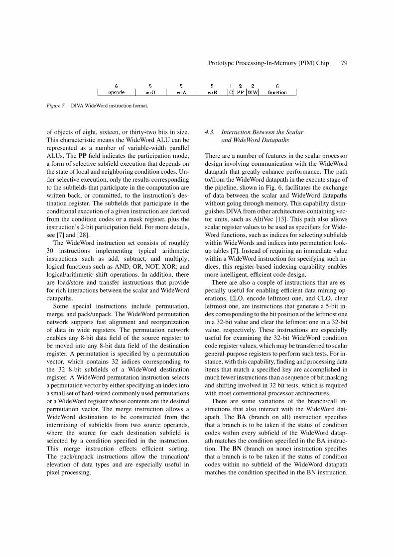
Similar to scalar instructions and as shown in Fig. 7,most DIVA WideWord instructions use a three-operandformat to specify two 256-bit source registers and a256-bit destination register. The opcode generally de-notes a class of operations, such as arithmetic, and thefunction denotes a specific operation, such as add orsubtract. The C bit indicates whether the operation per-formed by the instruction execution updates conditioncodes. The WW field indicates the operand width, al-lowing WideWord data to be treated as a packed array
Prototype Processing-In-Memory (PIM) Chip 79
Figure 7. DIVA WideWord instruction format.
of objects of eight, sixteen, or thirty-two bits in size.This characteristic means the WideWord ALU can berepresented as a number of variable-width parallelALUs. The PP field indicates the participation mode,a form of selective subfield execution that depends onthe state of local and neighboring condition codes. Un-der selective execution, only the results correspondingto the subfields that participate in the computation arewritten back, or committed, to the instruction’s des-tination register. The subfields that participate in theconditional execution of a given instruction are derivedfrom the condition codes or a mask register, plus theinstruction’s 2-bit participation field. For more details,see [7] and [28].
The WideWord instruction set consists of roughly30 instructions implementing typical arithmeticinstructions such as add, subtract, and multiply;logical functions such as AND, OR, NOT, XOR; andlogical/arithmetic shift operations. In addition, thereare load/store and transfer instructions that providefor rich interactions between the scalar and WideWorddatapaths.
Some special instructions include permutation,merge, and pack/unpack. The WideWord permutationnetwork supports fast alignment and reorganizationof data in wide registers. The permutation networkenables any 8-bit data field of the source register tobe moved into any 8-bit data field of the destinationregister. A permutation is specified by a permutationvector, which contains 32 indices corresponding tothe 32 8-bit subfields of a WideWord destinationregister. A WideWord permutation instruction selectsa permutation vector by either specifying an index intoa small set of hard-wired commonly used permutationsor a WideWord register whose contents are the desiredpermutation vector. The merge instruction allows aWideWord destination to be constructed from theintermixing of subfields from two source operands,where the source for each destination subfield isselected by a condition specified in the instruction.This merge instruction effects efficient sorting.The pack/unpack instructions allow the truncation/elevation of data types and are especially useful inpixel processing.
4.3. Interaction Between the Scalarand WideWord Datapaths
There are a number of features in the scalar processordesign involving communication with the WideWorddatapath that greatly enhance performance. The pathto/from the WideWord datapath in the execute stage ofthe pipeline, shown in Fig. 6, facilitates the exchangeof data between the scalar and WideWord datapathswithout going through memory. This capability distin-guishes DIVA from other architectures containing vec-tor units, such as AltiVec [13]. This path also allowsscalar register values to be used as specifiers for Wide-Word functions, such as indices for selecting subfieldswithin WideWords and indices into permutation look-up tables [7]. Instead of requiring an immediate valuewithin a WideWord instruction for specifying such in-dices, this register-based indexing capability enablesmore intelligent, efficient code design.
There are also a couple of instructions that are es-pecially useful for enabling efficient data mining op-erations. ELO, encode leftmost one, and CLO, clearleftmost one, are instructions that generate a 5-bit in-dex corresponding to the bit position of the leftmost onein a 32-bit value and clear the leftmost one in a 32-bitvalue, respectively. These instructions are especiallyuseful for examining the 32-bit WideWord conditioncode register values, which may be transferred to scalargeneral-purpose registers to perform such tests. For in-stance, with this capability, finding and processing dataitems that match a specified key are accomplished inmuch fewer instructions than a sequence of bit maskingand shifting involved in 32 bit tests, which is requiredwith most conventional processor architectures.
There are some variations of the branch/call in-structions that also interact with the WideWord dat-apath. The BA (branch on all) instruction specifiesthat a branch is to be taken if the status of conditioncodes within every subfield of the WideWord datap-ath matches the condition specified in the BA instruc-tion. The BN (branch on none) instruction specifiesthat a branch is to be taken if the status of conditioncodes within no subfield of the WideWord datapathmatches the condition specified in the BN instruction.

80 Draper et al.
With proper code structuring around these instructions,inverse forms of these branches, such as branch on anyor branch on not all, can also be effected.
5. Implementation and Testing of a DIVAPrototype PIM Chip
To prove the merits of the DIVA design, a single-nodeSRAM-based PIM prototype was fabricated. This pro-totype contained not only the PIM processor describedin previous sections, but also all components shownin Figs. 2 and 3. (Specific implementation details forthe processing subcomponents have appeared in ear-lier literature [14, 15].) The specification for this pro-totype PIM chip required on the order of 40,000 linesof VHDL code, consisting of a mix of RTL-level be-havioral and gate-level structural code. The VHDLwas optimized and synthesized using Synopsys De-sign Compiler, targeting the Artisan standard cell li-brary for TSMC 0.18 µm technology. The entire chipwas placed and routed, including clock tree routing,with Cadence Silicon Ensemble. Physical validation,including design rule checking (DRC), layout versusschematic (LVS) verification, and antennae checking,was performed with Mentor Calibre. In addition to Ar-tisan standard cells, the intellectual property buildingblocks used in the chip include two instances of a Vi-rage Logic 4 Mb SRAM macro, a NurLogic PLL clockmultiplier, and Artisan I/O cells and register files. Theresulting chip shown in Fig. 8 was fabricated throughMOSIS in TSMC 0.18 µm technology, and the silicon
Figure 8. DIVA PIM prototype chip.
die measures 9.8 mm on a side. It contains approxi-mately 2 million logic transistors and 53 million tran-sistors in the node SRAM. The chip pinout consists of352 pads, of which 240 are signal I/O, and the chippackage is a 35 mm ball grid array (BGA) from ASAT,Inc.
To quickly demonstrate system operation, SODIMMmodules containing 2 PIMs each were fabricated andinserted into an existing, custom PPC603e computeboard, shown in Fig. 9. In early testing, the PIM chips
Figure 9. PIM development system components.

Prototype Processing-In-Memory (PIM) Chip 81
easily achieved their first-order goal of appearing asstandard SDRAM devices, completing read/write re-quests from the PPC603e and the associated MPC106memory controller just as any other standard SDRAMmodule. For initial performance evaluation, an exam-ple 32 kbyte matrix transpose operation was executedon both the PPC603e and a single PIM device. The PIMdemonstrated a 35x speedup for this application whiledissipating only 0.8 W at 160 MHz, a significant resultas matrix transpose occurs frequently in many signalprocessing applications. Much of this speedup resultis due to the relative memory access times betweenthe system PPC processor and the PIM processor. ThePPC data cache is ineffective for the matrix transposeoperation, which exhibits very little temporal reuse ofdata, so the PPC spends much of its time in memory ac-cesses. Given that the PIM processor can access mem-ory with much less latency than the off-chip systemPPC, a significant speedup results. Secondly, the PIMimplementation of the matrix transpose operation wasimplemented using WideWord accesses and exploitingfeatures such as the permutation functions and tightintegration of the scalar and WideWord units, as dis-cussed in Sections 4.2 and 4.3. Such features result in adramatic decrease in computation time. Comparisonsof code execution on the PIM WideWord unit versus thescalar processor show that a 7x speedup factor resultsfrom these WideWord features [7].
Other demonstration kernels such as Transitive Clo-sure, Field, Pointer, and StreamAdd have been portedto the PIM devices, and some of these codes have evenbeen executed on multiple PIMs in a multiprocess-ing fashion, validating the communication infrastruc-ture of the PIM devices. While instrumented perfor-mance measurements are still being conducted, pro-jected results from earlier system simulation can befound in [7, 8].
6. Related Work
The DIVA approach is distinguished from other effortsin a number of manners. Integration into a conventionalsystem affords the simultaneous benefits of PIM tech-nology and a state-of-the-art host, yielding high per-formance for mixed workloads. Since PIM processorsare usually less sophisticated than state-of-the-art pro-cessors due to on-chip area constraints, systems usingPIMs alone in a multiprocessor may sacrifice perfor-mance on uniprocessor computations [16–19]. DIVA’s
support for a broad range of familiar parallel program-ming paradigms, including task parallelism for irreg-ular computations, distinguishes it from systems withrestricted applicability (such as to SIMD parallelism[20–22]), as well as those requiring a novel program-ming methodology or compiler technology to config-ure logic [23], or to manage a complex memory, com-putation and communication hierarchy [24]. DIVA’sPIM-to-PIM interconnect improves upon approachesthat serialize communication through the host, whichdecreases bandwidth by adding traffic to the processor-memory bus [21, 25], and allows the aggregation ofmany PIM devices, distinguishing the DIVA approachfrom designs intended primarily for system-on-a-chip(SOC) applications [22].
DIVA’s WideWord unit contains a number of fea-tures that distinguish it from commercial multimediaextensions that support superword parallelism, Pow-erPC AltiVec and Intel SSE2, as well as a previousresearch design called ASAP [26]. (Most other multi-media extensions support subword parallelism, whichperforms parallel operations on subfields of a machineword.) The ASAP combines WideWord and scalar ca-pabilities in a single unit. This approach eliminates theneed for transfers between register files, but with regis-ter forwarding, it can complicate the pipeline and slowdown the clock rate. All other implementations haveseparate scalar and WideWord units and register files,and other than DIVA, only SSE2 includes transfersbetween register files. The absence of such capabil-ity was reported to be a performance bottleneck in theAltiVec [27]. In addition, DIVA supports forms of per-mutation operations and selective execution that aremore efficient than those of alternative designs. Re-fer to the literature for more details concerning dis-tinguishing features as well as projected performancefrom system simulation [7, 8].
7. Conclusion
This paper has presented the design of a PIM proces-sor and implementation of a resulting prototype PIMchip used in the DIVA system, an integrated hard-ware and software architecture for exploiting the band-width of PIM-based systems. Although the processordesign bears some similarity to the combination of astandard 32-bit RISC processor with a 256-bit multi-media extension unit, it has a number of special fea-tures that make it well-suited for PIM processing. A

82 Draper et al.
working chip implementation of this architecture,based on TSMC 0.18 µm technology, has proven thevalidity of the design. The resulting workstation sys-tem architecture that incorporates such PIM devicesis projected to achieve speedups ranging from 8.8to 38.3 over conventional workstations for a numberof applications [7, 8]. These results demonstrate thatby sacrificing a small amount of area for process-ing logic on memory chips, PIM-based systems area technically viable method for combating the mem-ory wall problem. As memory bus standards progress,future technical challenges revolve around the designof PIM interfaces for those memory buses that allowPIMs and the host system processor(s) to share dataefficiently.
Given the encouraging success of the first DIVA PIMprototype chip and system integration, future work iscontinuing along several fronts. A second PIM proto-type which includes WideWord single-precision float-ing point capability and a PC266 DDR-SDRAM inter-face is due to tape out in August 2003. DIMM modulescontaining these PIMs are to be inserted into a Hewlett-Packard Itanium2-based Long’s Peak server for furtherapplication development. Continuing work on the cur-rent development system includes instrumented mea-surements for many of the ported applications.
Acknowledgments
The authors would like to acknowledge the supportof the DIVA project team and DARPA (Contract No.F30602-98-2-0180).
References
1. D. Burger, J. Goodman, and A. Kagi, “Memory Bandwidth Lim-itations of Future Microprocessors,” in Proceedings of the 23rdInternational Symposium on Computer Architecture, May 1996.
2. S. Iyer and H. Kalter, “Embedded DRAM Technology,” IEEESpectrum, April 1999, pp. 56–64.
3. P. Ranganathan, S. Adve, and N. Jouppi, “Performance of Imageand Video Processing with General-Purpose Processors and Me-dia ISA Extensions,” in Proceedings of the International Sym-posium on Computer Architecture, May 1999.
4. J.B. Carter et al., “Impulse: Building a Smarter Memory Con-troller,” in Proceedings of the Fifth International Symposium onHigh Performance Computer Architecture, Jan. 1999, pp. 70–79.
5. T. von Eicken, D. Culler, S.C. Goldstein, and K. Schauser, “Ac-tive Messages: A Mechanism for Integrated Communication andComputation,” Proceedings of the 19th International Symposiumon Computer Architecture, May 1992.
6. C. Kang and J. Draper, “A Fast, Simple Router for the Data-Intensive Architecture (DIVA) System,” in Proceedings of theIEEE Midwest Symposium on Circuits and Systems, Aug. 2000.
7. J. Draper et al., “The Architecture of the DIVA Processing-in-Memory Chip,” in Proceedings of the International Conferenceon Supercomputing, June 2002, pp. 14–25.
8. Mary Hall et al., “Mapping Irregular Application to DIVA,a PIM-based Data-Intensive Architecture,” Supercomputing,Nov. 1999.
9. M. Hall and C. Steele, “Memory Management in a PIM-BasedArchitecture,” in Proceedings of the Workshop on IntelligentMemory Systems, Oct. 2000.
10. JEDEC, “JEDEC,” http://www.jedec.org.11. J. Hennessy and D. Patterson, Computer Architecture: A Quan-
titative Approach, 2nd edn., Morgan Kaufman, 1996.12. R. Lee et al., “Subword Parallelism with MAX-2,” IEEE Micro,
Aug. 1996, pp. 51–59.13. AltiVec, “AltiVec Technology,” http://www.altivec.org.14. J. Draper et al., “Implementation of a 32-bit RISC Proces-
sor for the Data-Intensive Architecture Processing-In-MemoryChip,” in Proceedings of the IEEE International Conferenceon Application-Specific Systems, Architectures, and Processors,July 2002, pp. 163–172.
15. J. Draper, J. Sondeen, and C. Kang, “Implementation of a 256-bit WideWord Processor for the Data-Intensive Architecture(DIVA) Processing-In-Memory (PIM) Chip,” in Proceedings ofthe 28th European Solid-State Circuit Conference, Sept. 2002,pp. 77–80.
16. IBM, “Blue Gene,” http://researchweb.watson.ibm.com/bluegene/.
17. P. Kogge, “The EXECUBE Approach to Massively Parallel Pro-cessing,” in Proceedings of the International Conference on Par-allel Processing, Aug. 1994.
18. A. Saulsbury, F. Pong, and A. Nowatzyk, “Missing the MemoryWall: The Case for Processor/Memory Integration,” in Proceed-ings of the International Symposium on Computer Architecture,May 1996.
19. T. Sterling, “An Introduction to the Gilgamesh PIM Architec-ture,” Euro-Par, 2001, pp. 16–32.
20. D. Elliott et al., “Computational RAM: Implementing Proces-sors in Memory,” IEEE Design and Test of Computers, January–March 1999, pp. 32–41.
21. M. Gokhale, B. Holmes, and K. Iobst, “Processing In Memory:the Terasys Massively Parallel PIM Array,” IEEE Computer,April 1995, pp. 23–31.
22. C. Kozyrakis et al., “Hardware/Compiler Co-development foran Embedded Media Processor,” in Proceedings of the IEEE,Nov. 2001, pp. 1694–1709.
23. J. Babb et al., “Parallelizing Applications into Silicon,” in Pro-ceedings of the IEEE Workshop on FPGAs for Custom Comput-ing Machines, April 1999.
24. Y. Kang et al., “FlexRAM: Toward an Advanced IntelligentMemory System,” in Proceedings of the IEEE InternationalConference on Computer Design, Oct. 1999.
25. M. Oskin, F.T. Chong, and T. Sherwood, “Active Pages: AModel of Computation for Intelligent Memory,” in Proceedingsof the International Symposium on Computer Architecture, June1998.
26. J. Brockman et al., “Microservers: A New Memory Seman-tics for Massively Parallel Computing,” in Proceedings of the
Prototype Processing-In-Memory (PIM) Chip 83
International Conference on Supercomputing, June 1999, pp.454–463.
27. S. Larsen and S. Amarasinghe, “Exploiting Superword-LevelParallelism with Multimedia Instruction Sets,” in Proceedingsof the ACM Conference on Programming Languages Design andImplementation, 2000.
28. J. Chame, M. Hall, and J. Shin, “Code Transformations for Ex-ploiting Bandwidth in PIM-Based Systems,” in Proceedings ofthe ISCA Workshop on Solving the Memory Wall Problem, June2000.
Jeffrey Draper is a Research Assistant Professor in the Departmentof Electrical Engineering at the University of Southern California. Heholds this appointment in conjunction with a Project Leader positionat the Information Sciences Institute of the University of SouthernCalifornia. Dr. Draper’s research group has participated in manyDARPA-sponsored large-scale VLSI development efforts. He is amember of the IEEE Computer Society and has conducted researchin the areas of processing-in-memory architectures, thermal manage-ment, VLSI, interconnection networks, and modeling/performanceevaluation. Dr. Draper received a BSEE from Texas A&M Universityand an MS and PhD from the University of Texas at [email protected]
J. Tim Barrett is a Senior Electrical Engineer at the InformationSciences Institute of the University of Southern California. Mr.Barrett has managed, designed and implemented the hardware, low-level software and integration of many computer systems. Appli-cations of these systems include scalable supercomputers at USCInformation Sciences Institute, the long distance telephone switchat AT&T Bell Labs, building energy management at Barber-ColmanCompany, and laser entertainment performance instruments at AuraTechnologies and Laser Images Inc. He is a member of IEEE SolidState Circuits Society and received his MSCS from the Universityof Illinois Chicago and BSEE from the University of [email protected]
Jeff Sondeen is a Research Associate at the Information SciencesInstitute of the University of Southern California, where he sup-ports and maintains CAD technology files, libraries, and tools forimplementing VLSI designs. Previously he has worked at SiliconCompilers and Hewlett-Packard in CAD tool and test chip develop-ment. He received an MSEE from the University of [email protected]
Sumit Mediratta is currently pursuing a PhD in Electrical Engineer-ing at the University of Southern California. He received a Bache-lor of Engineering degree in Electronics and Telecommunicationfrom the Shri Govind Ram Sekseria Institute of Technology and Sci-ence, India. His research interests include interconnection networks,VLSI, processing-in-memory architectures, high-speed data com-munication and synchronization techniques and network interfacesfor high-performance [email protected]
Chang Woo Kang received a BS in electrical engineering fromChung-ang University, Seoul, South Korea, in 1997 and an MS inelectrical engineering from the University of Southern California,Los Angeles, in 1999. He is currently pursuing a PhD in electricalengineering at the University of Southern California. His researchincludes VLSI system design and algorithms for low-power logicsynthesis and physical [email protected]
84 Draper et al.
Ihn Kim is a PhD student in the Department of Electrical Engineeringat the University of Southern California. He is also a Staff Engineer atQLogic. His research interests include user-level network interface,network processor architectures, and modeling/performance evalua-tion of system area networks. He is a member of the IEEE ComputerSociety. He received an MS at KAIST (Korea Advanced Institute ofScience and Technology)[email protected]
Gokhan Daglikoca is an Application Engineer at Cadence DesignSystems, Inc, where he specializes in High-Performance ASIC andMicroprocessor Design Methodologies. He is a member of IEEE.Gokhan Daglikoca received a BS from Istanbul Technical Universityand an MS from the University of Southern [email protected]