voltage controlled oscillators - · pdf fileroot locus plot allows us to view closed loop...
TRANSCRIPT

M.H. Perrott
High Speed Communication Circuits and SystemsLecture 11
Voltage Controlled Oscillators
Michael H. PerrottMarch 10, 2004
Copyright © 2004 by Michael H. PerrottAll rights reserved.
1

M.H. PerrottM.H. Perrott
VCO Design for Wireless Systems
Design Issues- Tuning Range – need to cover all frequency channels- Noise – impacts receiver blocking and sensitivity performance- Power – want low power dissipation- Isolation – want to minimize noise pathways into VCO- Sensitivity to process/temp variations – need to make it
manufacturable in high volume
Zin
Zo LNA To Filter
From Antennaand Bandpass
Filter
PC boardtrace
PackageInterface
LO signal
MixerRF in IF out
FrequencySynthesizer
ReferenceFrequency
VCO
2

M.H. PerrottM.H. Perrott
VCO Design For High Speed Data Links
Design Issues- Same as wireless, but:
Required noise performance is often less stringent Tuning range is often narrower
Zin
Zo AmpFrom Broadband
Transmitter
PC boardtrace
PackageInterface
In Clock andData
Recovery
Data
Clk
LoopFilter
PhaseDetector
Data Out
Data In Clk Out
VCO
3

M.H. PerrottM.H. Perrott
Popular VCO Structures
Vout
VinC RpL-Ramp
VCO Amp
Vout
Vin
LC oscillator
Ring oscillator
-1
LC Oscillator: low phase noise, large area Ring Oscillator: easy to integrate, higher phase noise
4

M.H. PerrottM.H. Perrott
Barkhausen’s Criteria for Oscillation
Closed loop transfer function
Self-sustaining oscillation at frequency wo if
H(jw)x = 0 ye
e(t)
y(t)
Barkhausen Criteria
H(jwo) = 1
Asin(wot)
Asin(wot)
- Amounts to two conditions: Gain = 1 at frequency wo
Phase = n360 degrees (n = 0,1,2,…) at frequency wo
5

M.H. PerrottM.H. Perrott
Example 1: Ring Oscillator
Gain is set to 1 by saturating characteristic of inverters
Phase equals 360 degrees at frequency of oscillation
A B C
Δt (or ΔΦ)
A
B
C
A
A
T
- Assume N stages each with phase shift
- Alternately, N stages with delay t
6

M.H. PerrottM.H. Perrott
Further Info on Ring Oscillators
Due to their relatively poor phase noise performance, ring oscillators are rarely used in RF systems- They are used quite often in high speed data links,
though We will focus on LC oscillators in this lecture Some useful info on CMOS ring oscillators- Maneatis et. al., “Precise Delay Generation Using
Coupled Oscillators”, JSSC, Dec 1993 (look at pp 127-128 for delay cell description)- Todd Weigandt’s PhD thesis –
http://kabuki.eecs.berkeley.edu/~weigandt/
7

M.H. PerrottM.H. Perrott
Example 2: Resonator-Based Oscillator
Barkhausen Criteria for oscillation at frequency wo:
- Assuming Gm is purely real, Z(jwo) must also be purely real
Z(jw)
LpRp Cp
Vout
GmVx
-1
Vx
Z(jw)-Gm-10 VoutVx
8
M.H. PerrottM.H. Perrott
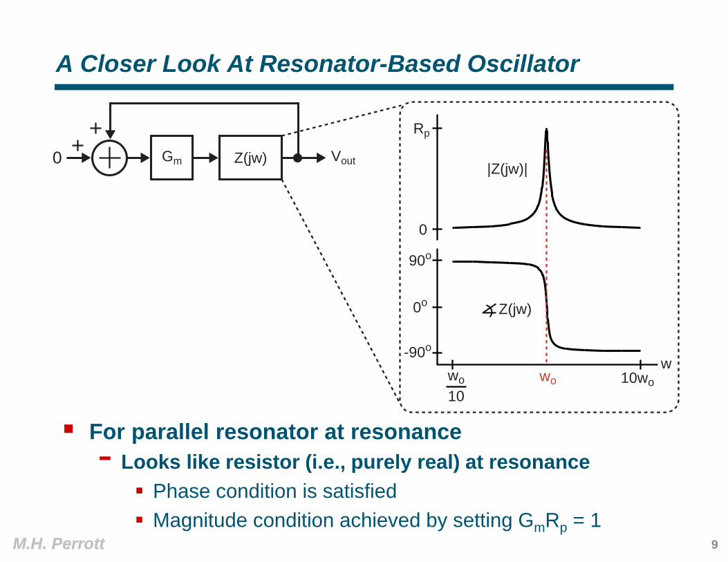
A Closer Look At Resonator-Based Oscillator
For parallel resonator at resonance- Looks like resistor (i.e., purely real) at resonance
Phase condition is satisfied Magnitude condition achieved by setting GmRp = 1
wo 10wowo10
|Z(jw)|
Z(jw)
90o
-90o
0
0o
Z(jw)Gm0 Vout
Rp
w
9

M.H. PerrottM.H. Perrott
Impact of Different Gm Values
Root locus plot allows us to view closed loop pole locations as a function of open loop poles/zero and open loop gain (GmRp)- As gain (GmRp) increases, closed loop poles move into
right half S-plane
Open LoopResonator
Poles and Zero
Locus ofClosed Loop
Pole Locations
Increasing GmRp
jw
σ
S-plane
10

M.H. PerrottM.H. Perrott
Impact of Setting Gm too low
Closed loop poles end up in the left half S-plane- Underdamped response occurs
Oscillation dies out
Open LoopResonator
Poles and Zero
GmRp < 1
Locus ofClosed Loop
Pole Locations
Closed Loop Step Responsejw
σ
S-plane
11
M.H. PerrottM.H. Perrott
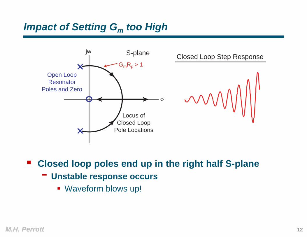
Impact of Setting Gm too High
Closed loop poles end up in the right half S-plane- Unstable response occurs
Waveform blows up!
Open LoopResonator
Poles and Zero
GmRp > 1
Locus ofClosed Loop
Pole Locations
Closed Loop Step Responsejw
σ
S-plane
12

M.H. PerrottM.H. Perrott
Setting Gm To Just the Right Value
Closed loop poles end up on jw axis- Oscillation maintained
Issue – GmRp needs to exactly equal 1- How do we achieve this in practice?
Open LoopResonator
Poles and Zero
GmRp = 1
Locus ofClosed Loop
Pole Locations
Closed Loop Step Responsejw
σ
S-plane
13

M.H. PerrottM.H. Perrott
Amplitude Feedback Loop
One thought is to detect oscillator amplitude, and then adjust Gm so that it equals a desired value- By using feedback, we can precisely achieve GmRp = 1
Issues- Complex, requires power, and adds noise
Adjustmentof Gm
Oscillator
PeakDetector
DesiredPeak Value
Output
14

M.H. PerrottM.H. Perrott
Leveraging Amplifier Nonlinearity as Feedback
Practical transconductance amplifiers have saturating characteristics- Harmonics created, but filtered out by resonator- Our interest is in the relationship between the input and
the fundamental of the output
0 woW
0 wo 2wo 3woW
Z(jw)
-Gm
-10 VoutVx Ix
|Vx(w)|
|Ix(w)|
A
GmA
15

M.H. PerrottM.H. Perrott
Leveraging Amplifier Nonlinearity as Feedback
As input amplitude is increased- Effective gain from input to fundamental of output drops- Amplitude feedback occurs! (GmRp = 1 in steady-state)
0 woW
0 wo 2wo 3woW
Z(jw)
-Gm
-10 VoutVx Ix
|Vx(w)|
|Ix(w)|
A
GmAA
GmA
Gm
A
GmRp=1
16

M.H. PerrottM.H. Perrott
One-Port View of Resonator-Based Oscillators
Convenient for intuitive analysis Here we seek to cancel out loss in tank with a
negative resistance element- To achieve sustained oscillation, we must have
Zres
ActiveNegative
ResistanceGenerator
Resonator
Zactive
Resonator
LpRp Cp
Vout
= -Rp
Active NegativeResistance
-Gm
1
ZresZactive
Vout
17

M.H. PerrottM.H. Perrott
One-Port Modeling Requires Parallel RLC Network
Since VCO operates over a very narrow band of frequencies, we can always do series to parallel transformations to achieve a parallel network for analysis
- Warning – in practice, RLC networks can have secondary (or more) resonant frequencies, which cause undesirable behavior Equivalent parallel network masks this problem in hand
analysis Simulation will reveal the problem
LpRp Cp
Ls
RsL
Cs
RsC
18

M.H. PerrottM.H. Perrott
Example – Negative Resistance Oscillator
This type of oscillator structure is quite popular in current CMOS implementations- Advantages
Simple topology Differential implementation (good for feeding differential
circuits) Good phase noise performance can be achieved
M1
L2
C2
Ibias
L1
M2C1Vs
Vout Vout
RL2RL1
RC1 RC2
M1
L2
C2
Ibias
L1
M2C1Vs
Vout Vout
Include lossin inductors and
capacitors
19

M.H. PerrottM.H. Perrott
Analysis of Negative Resistance Oscillator (Step 1)
Derive a parallel RLC network that includes the loss of the tank inductor and capacitor- Typically, such loss is dominated by series resistance in
the inductor
Lp1Rp1 Cp1
M1
Ibias
M2
Vs
Vout Vout
Lp2 Rp2Cp2
Narrowbandparallel RLC
model for tankM1
L2
C2
Ibias
L1
M2C1Vs
Vout Vout
RL2RL1
RC1 RC2
20

M.H. PerrottM.H. Perrott
Analysis of Negative Resistance Oscillator (Step 2)
Split oscillator circuit into half circuits to simplify analysis- Leverages the fact that we can approximate Vs as being
incremental ground (this is not quite true, but close enough) Recognize that we have a diode connected device with a
negative transconductance value- Replace with negative resistor
Note: Gm is large signal transconductance value
M1
Vout -1
Lp1Rp1 Cp1
Vout
Lp1Rp1 Cp1
-Gm1
1
Lp1Rp1 Cp1
M1
Ibias
M2
Vs
Vout Vout
21

M.H. PerrottM.H. Perrott
Design of Negative Resistance Oscillator
Design tank components to achieve high Q- Resulting Rp value is as large as possible Choose bias current (Ibias) for large swing (without going
far into saturation)- We’ll estimate swing as a function of Ibias shortly Choose transistor size to achieve adequately large gm1- Usually twice as large as 1/Rp1 to guarantee startup
Vout
Lp1Rp1 Cp1
-Gm1
1
Lp1Rp1 Cp1
M1
Ibias
M2
Vs
Vout Vout
Lp2 Rp2Cp2
Gm1
A
Gm1Rp1=1
gm1
A A
22

M.H. PerrottM.H. Perrott
Calculation of Oscillator Swing
Design tank components to achieve high Q- Resulting Rp value is as large as possible Choose bias current (Ibias) for large swing (without going
far into saturation)- We’ll estimate swing as a function of Ibias in next slide Choose transistor size to achieve adequately large gm1- Usually twice as large as 1/Rp1 to guarantee startup
Lp1Rp1 Cp1
M1
Ibias
M2Vs
Vout Vout
Lp2 Rp2Cp2
I2(t)I1(t)A A
23

M.H. PerrottM.H. Perrott
Calculation of Oscillator Swing as a Function of Ibias
By symmetry, assume I1(t) is a square wave- We are interested in determining fundamental component
(DC and harmonics filtered by tank)
- Fundamental component is
- Resulting oscillator amplitude
f
T1
tTT
W=T/2
Ibias/2
Ibias/2I1(t)
Ibias
π1
3π1
|I1(f)|
IbiasIbias
Ibias
W1
24

M.H. PerrottM.H. Perrott
Variations on a Theme
Biasing can come from top or bottom Can use either NMOS, PMOS, or both for transconductor- Use of both NMOS and PMOS for coupled pair would appear to
achieve better phase noise at a given power dissipation See Hajimiri et. al, “Design Issues in CMOS Differential LC
Oscillators”, JSSC, May 1999 and Feb, 2000 (pp 286-287)
M1
L2
C2
Ibias
L1
M2C1Vs
Vout Vout
M1
L2
C2
Ibias
L1
M2C1
Vout Vout
M1
Ld
C2M2C1
Vout Vout
M4M3
Ibias
Bottom-biased NMOS Top-biased NMOS Top-biased NMOS and PMOS
25

M.H. PerrottM.H. Perrott
Colpitts Oscillator
Carryover from discrete designs in which single-ended approaches were preferred for simplicity- Achieves negative resistance with only one transistor- Differential structure can also be implemented
Good phase noise can be achieved, but not apparent there is an advantage of this design over negative resistance design for CMOS applications
L
C1
Ibias
M1
Vout
Vbias
C2
V1
26

M.H. PerrottM.H. Perrott
Analysis of Cap Transformer used in Colpitts
Voltage drop across RL is reduced by capacitive voltage divider- Assume that impedances of caps are less than RL at
resonant frequency of tank (simplifies analysis) Ratio of V1 to Vout set by caps and not RL
Power conservation leads to transformer relationship shown
L
C2
C1
RL
V1Vout
RL
1:N
Rin= N21 RL
V1=NVout
L C1||C2VoutLVout
C1||C2
N21 RL
N =C1
C1+C2
C1C2
C1+C2C1||C2 =
27

M.H. PerrottM.H. Perrott
Simplified Model of Colpitts
C1
Ibias
M1
Vout
Vbias
C2
V1
M1
vout
v1
C1||C2
Nvout
id1
RpL
1/Gm
1/Gm
N2
N=C1
C1+C2
C1C2
C1+C2C1||C2 =
vout
-GmNvout
Rp||1/Gm
N2
-1/GmN
vout
Rp||1/Gm
N2
L C1||C2 L
C1||C2 L
Includeloss in tank
Purpose of cap transformer- Reduces loading on tank- Reduces swing at source node
(important for bipolar version)
Transformer ratio set to achieve best noise performance28

M.H. PerrottM.H. Perrott
Design of Colpitts Oscillator
AI1(t)
C1
Ibias
M1
Vout
Vbias
C2
V1
L
1/Gm
Gm1
A
NGm1Req=1
gm1
-1/GmN
vout
Req=C1||C2 L Rp||1/Gm
N2
Design tank for high Q Choose bias current (Ibias) for large swing (without going
far into saturation) Choose transformer ratio for best noise- Rule of thumb: choose N = 1/5 according to Tom Lee
Choose transistor size to achieve adequately large gm129

M.H. PerrottM.H. Perrott
Calculation of Oscillator Swing as a Function of Ibias
I1(t) consists of pulses whose shape and width are a function of the transistor behavior and transformer ratio - Approximate as narrow square wave pulses with width W
- Fundamental component is
- Resulting oscillator amplitude
tTT
W
f
T1
Ibias
I1(t)
average = Ibias
|I1(f)|
Ibias
W1
30

M.H. PerrottM.H. Perrott
Clapp Oscillator
Same as Colpitts except that inductor portion of tank is isolated from the drain of the device- Allows inductor voltage to achieve a larger amplitude
without exceeded the max allowable voltage at the drain Good for achieving lower phase noise
C1
Ibias
M1
Vout
Vbias
C2
V1
L
1/Gm
C3
L Llarge
31

M.H. PerrottM.H. Perrott
C1
Ibias
M1
Vout
Vbias
C2
V1
M1
vout
v1
C1||C2
Nvout
id1
Rp
L
1/Gm
1/Gm
N2
N=C1
C1+C2
C1C2
C1+C2C1||C2 =
vout
-GmNvout
Rp||1/Gm
N2
-1/GmN
vout
Rp||1/Gm
N2
C3CpLp Cp+C1||C2 Lp
Cp+C1||C2 Lp
L Llarge
Simplified Model of Clapp Oscillator
Looks similar to Colpitts model- Be careful of parasitic resonances!
32

M.H. PerrottM.H. Perrott
Hartley Oscillator
Same as Colpitts, but uses a tapped inductor rather than series capacitors to implement the transformer portion of the circuit- Not popular for IC implementations due to the fact that
capacitors are easier to realize than inductors
L1
Ibias
M1
Vout
Vbias
L2
V1
Cbig
C
33

M.H. PerrottM.H. Perrott
L1
Ibias
M1
Vout
Vbias
L2
M1
vout
v1
Nvout
id1
Rp
1/Gm
N2
N=L2
L1+L2
vout
-GmNvout
Rp||1/Gm
N2
-1/GmN
vout
Rp||1/Gm
N2
L1+L2
C C L1+L2
C L1+L2
V1
Cbig
C
Simplified Model of Hartley Oscillator
Similar to Colpitts, again be wary of parasitic resonances
34

M.H. PerrottM.H. Perrott
Integrated Resonator Structures
Inductor and capacitor tank- Lateral caps have high Q (> 50)- Spiral inductors have moderate Q (5 to 10), but
completely integrated and have tight tolerance (< ± 10%)- Bondwire inductors have high Q (> 40), but not as
“integrated” and have poor tolerance (> ± 20%)- Note: see Lecture 4 for more info on these
B
A
C1
A
B
Lm
A
B
B
A
Lateral Capacitor Spiral Inductor Bondwire Inductor
die
package
35

M.H. PerrottM.H. Perrott
Integrated Resonator Structures
Integrated transformer- Leverages self and mutual inductance for resonance to
achieve higher Q- See Straayer et. al., “A low-noise transformer-based 1.7
GHz CMOS VCO”, ISSCC 2002, pp 286-287
A B
L2
B
L1
A
Cpar1
k C D
C DCpar2
36

M.H. PerrottM.H. Perrott
Quarter Wave Resonator
Impedance calculation (from Lecture 4)
- Looks like parallel LC tank! Benefit – very high Q can be achieved with fancy
dielectric Negative – relatively large area (external implementation
in the past), but getting smaller with higher frequencies!
x
z
y
ZL
0Lz
λ0/4
Z(λ0/4)
37

M.H. PerrottM.H. Perrott
Other Types of Resonators
Quartz crystal- Very high Q, and very accurate and stable resonant
frequency Confined to low frequencies (< 200 MHz) Non-integrated
- Used to create low noise, accurate, “reference” oscillators SAW devices- High frequency, but poor accuracy (for resonant frequency)
MEMS devices- Cantilever beams – promise high Q, but non-tunable and
haven’t made it to the GHz range, yet, for resonant frequency- FBAR – Q > 1000, but non-tunable and poor accuracy- Other devices are on the way!
38
M.H. PerrottM.H. Perrott
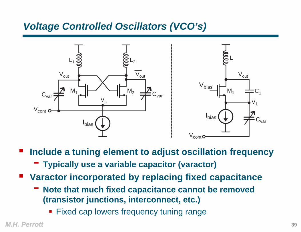
Voltage Controlled Oscillators (VCO’s)
Include a tuning element to adjust oscillation frequency- Typically use a variable capacitor (varactor)
Varactor incorporated by replacing fixed capacitance- Note that much fixed capacitance cannot be removed
(transistor junctions, interconnect, etc.) Fixed cap lowers frequency tuning range
M1
L2
Ibias
L1
M2
Vs
Vout Vout
Cvar Cvar
L
C1
Ibias
M1
Vout
Vbias
V1
Cvar
Vcont
Vcont
39

M.H. PerrottM.H. Perrott
Model for Voltage to Frequency Mapping of VCO
Model VCO in a small signal manner by looking at deviations in frequency about the bias point- Assume linear relationship between input voltage and
output frequency
M1
L2
Ibias
L1
M2
Vs
Vout Vout
Cvar Cvar
Vcont
Vbias
Vin
T=1/FvcoVCO frequency versus Vcont
slope=Kv
VbiasVcont
Fvco
Foutfo
Vin
40

M.H. PerrottM.H. Perrott
Model for Voltage to Phase Mapping of VCO
1/Fvco= α
1/Fvco= α+ε
out(t)
out(t)
Intuition of integral relationship between frequency and phase
Phase is more convenient than frequency for analysis- The two are related through an integral relationship
41

M.H. PerrottM.H. Perrott
Frequency Domain Model of VCO
Take Laplace Transform of phase relationship
- Note that Kv is in units of Hz/V
Frequency DomainVCO Model
M1
L2
Ibias
L1
M2
Vs
Vout Vout
Cvar Cvar
Vcont
Vbias
Vin
T=1/Fvco
2πKvs
vin Φout
42

M.H. PerrottM.H. Perrott
Varactor Implementation – Diode Version
Consists of a reverse biased diode junction- Variable capacitor formed by depletion capacitance- Capacitance drops as roughly the square root of the
bias voltage Advantage – can be fully integrated in CMOS Disadvantages – low Q (often < 20), and low tuning
range (± 20%)
P+ N+
P- substrate
DepletionRegion
V-
V+
N- n-wellV-
V+
V+-V-
Cvar
43

M.H. PerrottM.H. Perrott
A Recently Popular Approach – The MOS Varactor
Consists of a MOS transistor (NMOS or PMOS) with drain and source connected together- Abrupt shift in capacitance as inversion channel forms
Advantage – easily integrated in CMOS Disadvantage – Q is relatively low in the transition
region- Note that large signal is applied to varactor – transition
region will be swept across each VCO cycle
N+ N+
P-DepletionRegion
V-
V+
VTV+-V-
Cdep
Cox
Cvar
W/L
V-
V+
44

M.H. PerrottM.H. Perrott
A Method To Increase Q of MOS Varactor
High Q metal caps are switched in to provide coarse tuning
Low Q MOS varactor used to obtain fine tuning See Hegazi et. al., “A Filtering Technique to Lower LC
Oscillator Phase Noise”, JSSC, Dec 2001, pp 1921-1930
LSB
Vcontrol
W/LW/L
C
2W/L
2C
4W/L
4C
MSB
to VCO000001010011100101110111
Coarse Control Fine Control
CoarseControl
Cvar
VcontrolFine Control
Ove
rall
Cap
acita
nce
45

M.H. PerrottM.H. Perrott
Supply Pulling and Pushing
Supply voltage has an impact on the VCO frequency- Voltage across varactor will vary, thereby causing a
shift in its capacitance- Voltage across transistor drain junctions will vary,
thereby causing a shift in its depletion capacitance This problem is addressed by building a supply
regulator specifically for the VCO
M1
L2
Ibias
L1
M2
Vs
Vout Vout
Cvar Cvar
L
C1
Ibias
M1
Vout
Vbias
V1
Cvar
Vcont
Vcont
46

M.H. PerrottM.H. Perrott
Injection Locking
Noise close in frequency to VCO resonant frequency can cause VCO frequency to shift when its amplitude becomes high enough
VCO
Vout
Vnoise
Vinwo
W
|Vout(w)|
woW
|Vnoise(w)|
Δw Δw-Δw
woW
|Vout(w)|
woW
|Vnoise(w)|
Δw Δw-Δw
woW
|Vout(w)|
woW
|Vnoise(w)|
Δw Δw-Δw
woW
|Vout(w)|
woW
|Vnoise(w)|
Δw Δw-Δw
47

M.H. PerrottM.H. Perrott
Example of Injection Locking
For homodyne systems, VCO frequency can be very close to that of interferers
- Injection locking can happen if inadequate isolation from mixer RF input to LO port
Follow VCO with a buffer stage with high reverse isolation to alleviate this problem
wint0 woW
RF in(w) DesiredNarrowband
Signal
InterfererRF in
LO signal
LNA Mixer
LO frequencyVin
48